

Page 1
`
&
0
DOLBY B NR
ORDER NO.
RRV2199
STEREO CASSETTE DECK
CT-L77
THIS MANUAL IS APPLICABLE TO THE FOLLOWING MODEL(S) AND TYPE(S).
Type
ZVYXK DC power supplied from other system component
Model
CT-L77
Power Requirement
÷ This product does not operate normally by itself. Please connect it to the STEREO CD
RECEIVER XC-L77 , for adjustment and operation inspection. If operation confirmation
for the unit by itself can not be avoided, please follow the instructions on page 21.
Remarks
¶ This product is a system(s) component.
Be sure to connect it to the prescribed system component(s), otherwise damage may
result.
Component Model Service manual Remarks
STEREO CD RECEIVER XC-L77 RRV2187
S-L9-LRW — — RRV2176
SPEAKER SYSTEM — S-L9-A-LRW — RRV2176
— — S-L8-LRW RRV2178
STEREO CASSETTE DECK CT-L77 RRV2199 This manual.
MINIDISC RECORDER MJ-L77 RRV2201
CONTENTS
1. SAFETY INFORMATION
2. EXPLODED VIEWS AND PARTS LIST
3. BLOCK DIAGRAM AND SCHEMATIC DIAGRAM..10
4. PCB CONNECTION DIAGRAM
5. PCB PARTS LIST
6. ADJUSTMENT
...............................................
....................................................
......................................
................
..........................
16
19
21
2
3
7. GENERAL INFORMATION
7.1 DIAGNOSIS
7.1.1 POWER ON SEQUENCE
7.2 PARTS
7.2.1 IC
8. PANEL FACILITIES AND SPECIFICATIONS
............................................................
.................................................
.........................................................
................................
......................
....
26
26
26
27
27
28
PIONEER CORPORATION 4-1, Meguro 1-chome, Meguro-ku, Tokyo 153-8654, Japan
PIONEER ELECTRONICS SERVICE, INC. P.O. Box 1760, Long Beach, CA 90801-1760, U.S.A.
PIONEER ELECTRONIC (EUROPE) N.V. Haven 1087, Keetberglaan 1, 9120 Melsele, Belgium
PIONEER ELECTRONICS ASIACENTRE PTE. LTD. 253 Alexandra Road, #04-01, Singapore 159936
c
PIONEER CORPORATION 1999
T–ZZR AUG. 1999 Printed in Japan
Page 2
CT-L77
1. SAFETY INFORMATION
This service manual is intended for qualified service technicians ; it is not meant for the casual do-ityourselfer. Qualified technicians have the necessary test equipment and tools, and have been trained
to properly and safely repair complex products such as those covered by this manual.
Improperly performed repairs can adversely affect the safety and reliability of the product and may
void the warranty. If you are not qualified to perform the repair of this product properly and safely, you
should not risk trying to do so and refer the repair to a qualified service technician.
WARNING
This product contains lead in solder and certain electrical parts contain chemicals which are known to the state of California to cause
cancer, birth defects or other reproductive harm.
Health & Safety Code Section 25249.6 – Proposition 65
NOTICE
(FOR CANADIAN MODEL ONLY)
Fuse symbols (fast operating fuse) and/or (slow operating fuse) on PCB indicate that replacement parts must
be of identical designation.
REMARQUE
(POUR MODÈLE CANADIEN SEULEMENT)
Les symboles de fusible (fusible de type rapide) et/ou (fusible de type lent) sur CCI indiquent que les pièces
de remplacement doivent avoir la même désignation.
(FOR USA MODEL ONLY)
1. SAFETY PRECAUTIONS
The following check should be performed for the
continued protection of the customer and service
technician.
LEAKAGE CURRENT CHECK
Measure leakage current to a known earth ground (water
pipe, conduit, etc.) by connecting a leakage current tester
such as Simpson Model 229-2 or equivalent between the
earth ground and all exposed metal parts of the appliance
(input/output terminals, screwheads, metal overlays, control
shaft, etc.). Plug the AC line cord of the appliance directly
into a 120V AC 60Hz outlet and turn the AC power switch
on. Any current measured must not exceed 0.5mA.
Reading should
not be above
0.5mA
Earth
ground
Device
under
test
Also test with
plug reversed
(Using AC adapter
plug as required)
Leakage
current
tester
Test all
exposed metal
surfaces
ANY MEASUREMENTS NOT WITHIN THE LIMITS
OUTLINED ABOVE ARE INDICATIVE OF A POTENTIAL
SHOCK HAZARD AND MUST BE CORRECTED BEFORE
RETURNING THE APPLIANCE TO THE CUSTOMER.
2. PRODUCT SAFETY NOTICE
Many electrical and mechanical parts in the appliance
have special safety related characteristics. These are
often not evident from visual inspection nor the protection
afforded by them necessarily can be obtained by using
replacement components rated for voltage, wattage, etc.
Replacement parts which have these special safety
characteristics are identified in this Service Manual.
Electrical components having such features are identified
by marking with a
in this Service Manual.
The use of a substitute replacement component which does
not have the same safety characteristics as the PIONEER
recommended replacement one, shown in the parts list in
this Service Manual, may create shock, fire, or other hazards.
Product Safety is continuously under review and new
instructions are issued from time to time. For the latest
information, always consult the current PIONEER Service
Manual. A subscription to, or additional copies of, PIONEER
Service Manual may be obtained at a nominal charge from
PIONEER.
on the schematics and on the parts list
AC Leakage Test
2
Page 3
2. EXPLODED VIEWS AND PARTS LIST
NOTES:• Parts marked by "NSP" are generally unavailable because they are not in our Master Spare Parts List.
2.1 PACKING
The mark found on some component parts indicates the importance of the safety factor of the part.
•
Therefore, when replacing, be sure to use parts of identical designation.
Screws adjacent to mark on the product are used for disassembly.
•
6
CT-L77
5
4
1(1/2)
2(1/2)
2(2/2)
7
CT-L77
FRONT
1(2/2)
3
÷ PACKING PARTS LIST
Mark No. Description Part No.
1 Pad Front AHA7260
2 Pad Rear AHA7261
3 Packing Case AHD7767
4 Operating Instructions ARE7217
(Spanish/Portuguese/Dutch/Swedish/
English/French/German/Italian)
NSP 5 Warranty Card ARY7022
Mark No. Description Part No.
6 Polyethylene Bag Z21-038
(0.03 × 230 × 340)
7 Mirror Mat Sheet Z23-007
(750x600x0.5)
3
Page 4
CT-L77
2.2 EXTERIOR
18
28
26
27
11
30-2
17
2
10
13
25
19
30-1
16
23
Refer to "2.3 and 2.4
DECK MECHANISM
UNIT"
20
21
22
3
11
22
A
C
31
9
24
B
7
4
24
24
B
22
22
1
24
A
29
16
27
C
23
22
12
5
14
8
6
6
15
4
Page 5

÷ EXTERIOR PARTS LIST
Mark No. Description Part No.
1 MAIN UNIT AWU7391
2 KEY L UNIT AWU7392
3 KEY R UNIT AWU7393
4 Connection Cable ADE7043
5 Deck Mechanism Unit AXA7075
6 Foot AEB7090
7 Rear Panel ANC7827
NSP 8 Bottom Plate ANF7016
NSP 9 Top Plate ANF7017
10 BLUE IND. UNIT AWU7394
11 Main Line AAP7058
12 Cord Holder RNH-184
13 Tray Panel AAN7195
14 Tray Line AAP7059
15 Bottom Base AMA7014
16 Front Line AAP7066
17 Bonnet AMA7015
18 Button A Assy AWL7044
NSP 19 Tray Seal RRW1162
20 Button B Assy AWL7045
CT-L77
21 Screw BBT30P060FZK
22 Screw BBZ30P060FMC
23 Screw PPZ30P100FMC
24 Screw VPZ30P080FZK
25 CL Lens AAX7704
NSP 26 Button Lens AAX7703
NSP 27 Button AAD7528
NSP 28 Button Cap A AAP7063
NSP 29 Button Cap B AAP7064
30 Top Panel Assy AWL7051
NSP 30-1 Top Panel 1 AMB7645
NSP 30-2 Top Panel 2 AMB7646
31 Parallel Wire D20PYY0625E
5
Page 6
CT-L77
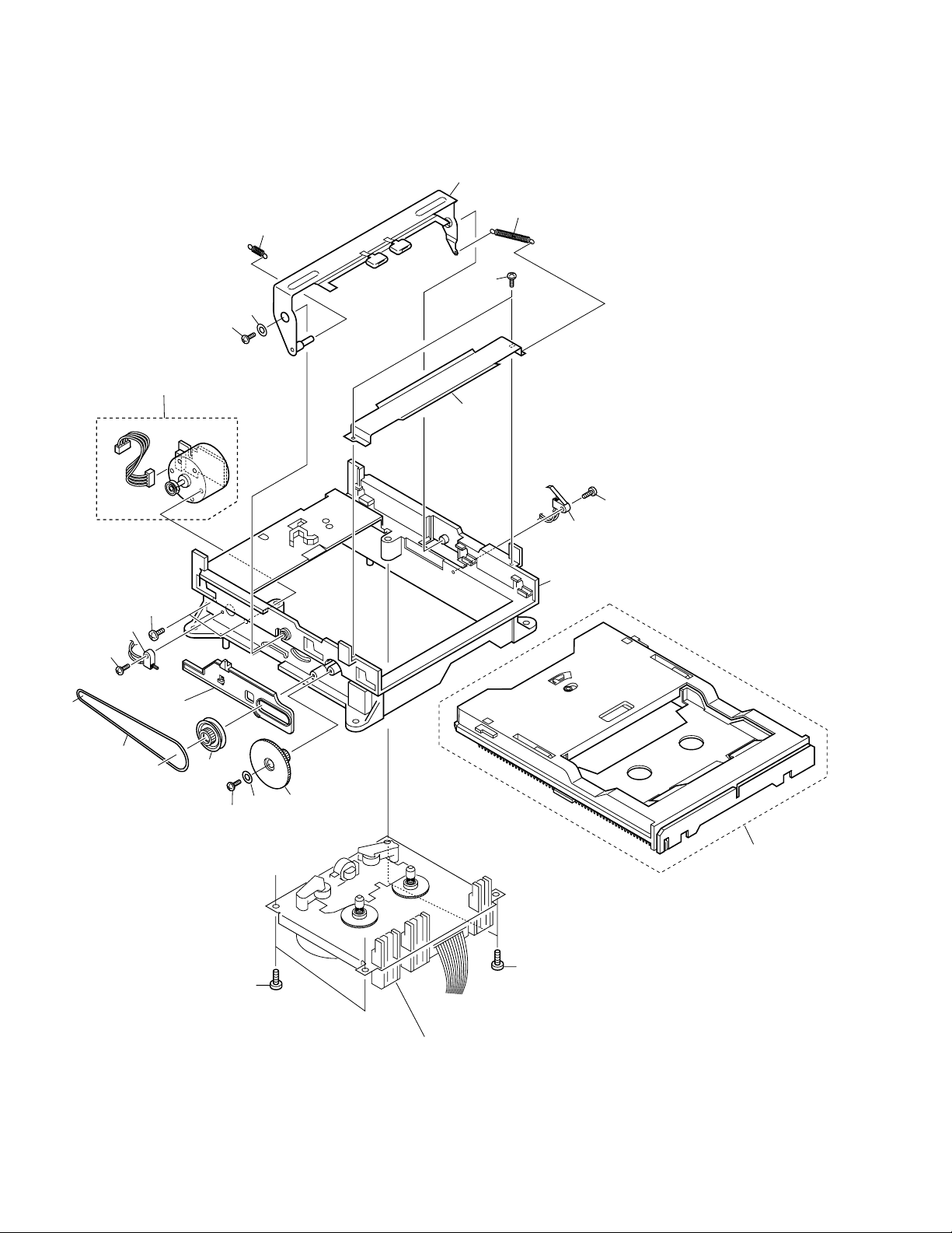
2.3 DECK MECHANISM UNIT (1/2)
17
4
16
14
6
5
16
3
16
12
13
16
18
8
1
11
9
4
16
10
7
2
2
Refer to "2.4. DECK MECHANISM UNIT (2/2).
6
Page 7

÷ DECK MECHANISM UNIT (1/2) PARTS LIST
Mark No. Description Part No.
1 Screw 2.6x5 FG114-14
2 Screw 2.6x6 UG12H-15
3 Front BKT FC64K-11
4 Washer 2.0 MJ112-22
5 SP Return FK34N-11
6 Plate Hold BLK F573-258
7 Holder CST BLK F527-078
8 LDG Base FD56R-12
9 Pulley FD56T-11
10 LDG Gear FD56U-11
11 Slider FD57E-11
12 LDG Belt FF19L-12
13 Switch UE15S-14
14 MTR Reel BLK F564-313
15 • • • • •
16 Screw 2.0x4 UG12H-28
17 SP Clamper FK34M-11
18 Switch UE18P-21
CT-L77
7
Page 8
CT-L77
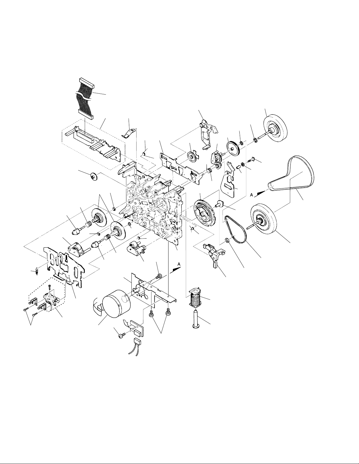
2.4 DECK MECHANISM UNIT (2/2)
39
40
19
33
15
12
31
10
4
2
32
2
8
23
5
14
31
32
7
9
3
18
34
11
6
16
24
21
43
35
37
36
30
13
20
30
41
42
27
22
26
9
17
28
1
29
1
3
25
38
8
Page 9

÷ DECK MECHANISM UNIT (2/2) PARTS LIST
Mark No. Description Part No.
1 Screw 2.0x6 KG194-36
2 Reel Feather FD57D-13
3 Screw 2.6x3.5 UG11S-14
4 SP Reel(L) FK32U-12
5 SP Brake FK33B-13
6 SP Arm Play FK33P-11
7 SP Reel(R) FK32V-12
8 Spring Cassette FC65M-11
9 BKT MTR FC64M-12
10 Reel Base FD52W-12
11 Cam Gear FD52Y-23
12 Play Gear (A) FD53K-12
13 Arm Play FD53D-19
14 Plate Slide FC61L-19
15 PCB Control BLK F567-617
16 Chassis base BLK F612-231
17 Head Base FC61K-32
18 Roller Pinch BLK R F514-129
19 Roller Pinch BLK L F514-130
20 Assy F/W FR24S-21
CT-L77
21 Clutch Assy BLK F522-037
22 Clutch Assy BLK F522-048
23 Washer 1.7x0.5 FJ111-13
24 F/R Pulley FD53F-15
25 Solenoid BLK F765-279
26 F/R Belt FF18W-12
27 Belt Main FF19H-11
28 Plate HD BLK F513-824
29 MTR MAIN BLK F525-321
30 Washer 2.6x0.25 FJ111-30
31 Washer 4.1x0.25 FJ111-35
32 Washer 1.75x0.4 UJ16F-11
33 Lever Brake FD53P-17
34 FF Gear(A) FD53L-12
35 Cam SP FK32S-14
36 Screw 2.0x0.3 UJ14A-12
37 Lever F/R FC62G-14
38 Plunger FL41S-21
39 Mecha-Cable WH65N-11
40 Spring HB FK32T-31
41 Screw 2.0x13 UG15V-13
42 Washer 2.0 MJ112-22
43 Spacer UJ15V-13
9
Page 10

1
23
CT-L77
3. BLOCK DIAGRAM AND SCHEMATIC DIAGRAM
3.1 BLOCK DIAGRAM and OVERALL SCHEMATIC DIAGRAM
4
A
B
REC/PB
HEAD
DECK
MECHANISM
UNIT
AXA7075
ERACE
HEAD
CN2301
3
4
2
1
CN2302
1
2
Lch
Rch
GNDA
GNDT
ATX7002
5
4
-72dBv
L2801
6
VR2801
VCP1164
220K-B
OFFSET
VR2802
VCP1164
220K-B
2
1
3
BIAS
BIAS OSC
Q2802
2SC1815
Q2803
2SC1815
VT-6
GNDA
Q2301
Q2301
2SK373
2SK373
D
D
G
G
Q2302
2SK373
D
G
VT+6
Q2805
2SA1048
Q2806
DTC124EK
BIAS
Q2804
2SC1815
S
S
VA+6
S
IC2441(1/2)
NJM4558MD
REC EQ
AMP
IC2441(2/2)
NJM4558MD
Q2307
DTA124EK
VA-6
1
VA+6
7
VA-6
8
4
GNDA
GNDA
2
5
6
3
GNDA
GNDA
GNDA
GNDA
VA+6
5
6
3
2
Q2447
2SD2144S
Q2448
2SD2144S
8
8
EQ
EQ
44
EQ
IC2301(1/2)
NJM4558MD
7
IC2301(2/2)
NJM4558MD
1
VA-6
VA+6
VA-6
BIAS
Q2303
DTC114TK
GNDA GNDA
PB AMP
Q2304
DTC114TK
GNDA
PB/REC
Q2443
DTC114TK
Q2444
DTC114TK
Q2305
DTC114TK
Q2306
DTC114TK
VR2401
VCP1158
22K-B
VR2442
VCP1158
Q2251
DTA124EK
PB/XREC
RECMUTE
-32.2dBv
VR2301
VCP1154
4.7K-B
PB LEVEL ADJ.
VR2302
PCP1154
4.7K-B
-3.7dBv
REC LEVEL ADJ.
22K-B
VA+6
Q2254
DTA124EK
GNDA
GNDA
GNDA
XCrO2
TAPE SPEED
VR2701
VCP1151
C
13
12
11
10
9
8
7
6
5
4
3
2
1
CN2602
6
HALL
13
12
11
10
9
8
7
6
5
4
3
2
1
1K-B
XMODE
GNDD
CN2603
D
1
2
3
4
5
5
1
4
2
3
3
2
4
1
5
VU+5
TOUT
XOPEN
XCLOSE
ADJ.
VM+6
XMOTOR
Q2712
2SB1425
XREC-R XREC-R
Q2705
DTA143EK
VM+6
Q2713
DTC124EK
GNDD
VM+6
Q2704
SOL
Q2714
DTA114EK
Q2702
Q2711
2SB1296
VM-6
CrO2
XHALF
XREC-F
XMODE
Q2701
LOADING
Q2701-2704
:2SD1858X
GNDM GNDM
Q2703
GNDD
X2501
VSS1045
6MHz
MECHA
CONT
V+5
Q2706
DTA143EK
SENS
CrO2(SW)
XHALF
XREC-F
XMODE
TOUT
TIN
XOPEN
XCLOSE
10
11
3
µ-COM
2
16
20
21
23
17
19
47
1
40
41
IC2701
PDC059A
NC
33
PB/XREC
43
RECMUTE
44
XCrO2
45
BIAS
46
39
4
26
28
XRESET XRESET
5
15
36
37
34
22
Q2502
DTC114TK
NC
25
DTC143EK
LEDPLAY
32
SERVICE KEY
14
NC
35
DKI–0
13
Q2503
V+5
V+5
DOL ON/OFF
S. CLOK(S)
D. CLOK(M)
D. DATA(M)
D. REQ (M)
VL-6
S. REQ
S. DATA
PB MUTE
VL+6
MS
CN2503
LEDPLAY
VL-6
VL+6
V+5
DKI–0
GNDD
1
2
3
4
5
6
10
1234
Page 11

5
678
CT-L77
Note : When ordering service parts, be sure to refer to "EXPLODED VIEWS and P AR TS LIST" or "PCB PARTS LIST".
:PLAYBACK SIGNAL ROUTE
GNDA
DOLBY-B NR
14
3
4
9
8
DTA124EK
GNDA
IC2201
HA12136AF
-3.7dBv
-32.2dBv
12
Q2202
Q2107
DTA124EK
11
+
6
+
IC2101(1/2)
NJM4558MD
ALC
16
GNDA
1
GNDA
5
VA+6
GNDA
5
6
VA+6
2PD601A
Q2103
2SC1740S
Q2104
2SC1740S
Q2108
DTC124EK
TP
-3.7dBv
TP
VA+6
8
4
VA-6
7
GNDA
F2201
RTF1209Q2102
MPX
F2202
RTF1209
MPX
MPX
A
2SD2144S
2SD2114K
3
2
36
36
Q2201
DTA124EK
(
A
1/2, A 2/2
Q2371
GNDAP GNDAP
Q2372
GNDAP
IC2101(2/2)
NJM4558MD
1
PB MUTE
Q2475
DTA124EK
VA-6
GNDD
MAIN UNIT
)
(AWU7391)
PB MUTE
MS
MS
DOL ON/OFF
V+5
XRESET
GNDD
Q2541
DTC124EK
RESET
BIAS
+
-4.8dBv
CN2601
GNDA
GNDP
PB OUT
Lch
PB OUT
Rch
REC R
GND AR
REC L
TC+
GND P
TC–
GNDDTC
NC
S. DATA
S. CLOCK
S. REQ
D. REQ
D. DATA
D. CLOCK
NC
:RECRDING SIGNAL ROUTE
19
18
17
16
15
14
13
12
11
10
9
8
7
6
5
4
3
2
1
TO CD RECEIVER XC–L77 or MD RECORDER MJ–L77
A
B
CN2901
VL-6
1
1
VL+6
2
2
LEDPLAY
3
3
V+5
4
4
DKI–0
5
5
GNDD
6
6
KEY L
UNIT : AWU7392
D2901 SLR-343MC
S2901
ASG7013
CHASSIS GND
VL-6
4
VL+6
3
2
1
GNDD
VT+6VL+6
J2902
VL-6
4
VL+6
3
KEYKEY
2
GNDD
1
VM+6VA+6
Q2003
2PB709A
GNDDGNDTGNDSGNDM
VM–6VA–6VT–6VL–6
KEY R
UNIT
: AWU7393
S2902
ASG7013
D2001
UDZS5.6B
Q2005
2PD601A
VL-6 VL-6
VL+6 VL+6
EJECT
V+5
Q2001
2SB1566
C
INOUT
IC2005
BAI7805T
OUT
IC2002
NJM7906FA
IN
BLUE IND
UNIT
J2903
1
1
2
2
: AWU7394
D2903 UDZ8.2B
D2902 EB3804X
D
11
5
6
7
8
Page 12

1
CT-L77
3.2 MAIN UNIT(1/2)
23
4
DECK
A
MECHANISM
UNIT (1/2)
(AXA7075)
B
A
MAIN UNIT (AWU7391)
1/2
C
D
12
A 1/2
1234
Page 13

5
678
CT-L77
A
2/2
B
A
C
SIGNAL ROUTE
: PLAYBACK SIGNAL
: RECORDING SIGNAL
D
A 1/2
5
6
7
8
13
Page 14

1
23
CT-L77
3.3 MAIN UNIT(2/2), KEYL UNIT, KEYR UNIT and BLUE IND UNIT
4
A
BLUE IND. UNIT
(AWU7394)
B
CD
KEYR UNIT
(AWU7393)
B
KEY L UNIT
(AWU7392)
C
: CHECK POINT for Service
D
SIGNAL ROUTE
: PLAYBACK SIGNAL
: RECORDING SIGNAL
14
A 2/2
1234
B
DECK
MECHANISM
UNIT (2/2)
(AXA7075)
C
D
Page 15

A
2/2
5
MAIN UNIT (AWU7391)
678
CT-L77
A
B
6.3V
–6.3V
–14V
5V
14V
1/2
A
C
To CD RECEIVER XC-L77 or MD RECORDER MJ-L77
: The power supply is shown with the marked box.
5
6
D
A 2/2
7
8
15
Page 16

1
23
CT-L77
4. PCB CONNECTION DIAGRAM
4.1 MAIN UNIT, KEYR UNIT, KEYL UNIT and BLUE IND UNIT
A
4
NOTE FOR PCB DIAGRAMS:
1. Part numbers in PCB diagrams match those in the schematic
diagrams.
2. A comparison between the main parts of PCB and schematic
diagrams is shown below.
Symbol in PCB
Diagrams
BCE
BCE
B
DGS
3. The parts mounted on this PCB include all necessary parts
for several destination.
For further information for respective destinations, be sure
to check with the schematic diagram.
4. Viewpoint of PCB diagrams
Symbol in Schematic
Diagrams
BCE
BCEBCE
DGSDGS
BCE
CapacitorConnector
Part Name
Transistor
Transistor
with resistor
Field effect
transistor
Resistor array
3-terminal
regulator
B
C
KEYR UNIT
KEYL UNIT
SIDE A
A
CN2503
SIDE A
C
P. C. Board Chip Part
SIDE B
D
BLUE IND UNIT
ANP7328–A
D
16
B
C D
1234
Page 17

1
234
CT-L77
SIDE A
Q2703
Q2701
Q2704
Q2702
IC2701
Q2103
Q2104
IC2201
IC2101
Q2371
Q2372
A
MAIN UNIT
To MECHANISM UNIT (LOADING MOTOR)
A
B
CN2901
B
To CD RECEIVER XC-L77 or
MD RECORDER MJ-L77
VR2441
VR2442
Q2447
Q2448
Q2301
Q2302
IC2441
VR2802
VR2801
IC2001
Q2805
Q2804
Q2802
Q2803
IC2005
VR2301
VR2302
IC2301
Q2711
Q2712
VR2701
IC2002
ANP7328–A
To MECHANISM UNIT
C
To MECHANISM UNIT
REC/PB HEAD
D
To MECHANISM UNIT
ERACE HEAD
A
1
2
3
4
17
Page 18

1
CT-L77
23
4
SIDE B
A
B
A
MAIN UNIT
IC2101
Q2475
Q2501
Q2371
Q2372
Q2502
Q2705
Q2706
IC2701
Q2503
Q2104
Q2253
Q2254
Q2251
IC2201
Q2741
Q2202
Q2201
Q2101
Q9451
Q2108
Q2107
Q2306
Q2714
IC2301
Q2305
Q2307
Q2305
C
D
ANP7328–A
Q2807
Q2447
Q2303
Q2304
Q2443
Q2301
Q2302
IC2441
Q2806
Q2005
Q2807
Q2804
Q2003
IC2005
Q2803
Q2802
18
A
1234
Page 19

CT-L77
Mark No. Description Part No.
Mark No. Description Part No.
5. PCB PARTS LIST
NOTES:•Parts marked by "NSP" are generally unavailable because they are not in our Master Spare Parts List.
Mark No. Description Part No.
LIST OF PCB ASSEMBLIES
NSP TC COMP ASSY AWM7450
MAIN UNIT
A
SEMICONDUCTORS
The mark found on some component parts indicates the importance of the safety factor of the part.
•
Therefore, when replacing, be sure to use parts of identical designation.
When ordering resistors, first convert resistance values into code form as shown in the following examples.
•
Ex.1 When there are 2 effective digits (any digit apart from 0), such as 560 ohm and 47k ohm (tolerance is shown by J=5%,
and K=10%).
560 Ω→56 × 10
47k Ω→47 × 10
1
→ 561 ........................................................RD1/4PU 5 6 1 J
3
→ 473 ........................................................RD1/4PU 4 7 3 J
0.5 Ω→R50 ..................................................................................... RN2H R 5 0 K
Ex.2 When there are 3 effective digits (such as in high precision metal film resistors).
5.62k Ω→ 562 × 10
1
→ 5621 ......................................................RN1/4PC 5 6 2 1 F
1 Ω→1R0 ..................................................................................... RS1P
1 R 0
Mark No. Description Part No.
COILS AND FILTERS
L2801 (OSC. COIL) ATX7002
MAIN UNIT AWU7391
KEY L UNIT AWU7392
KEY R UNIT AWU7393
BLUE IND. UNIT AWU7394
L2501 LAU100J
L2802 LFA121J
L2441, L2442 (10 mH) RTF1004
L2443, L2444 (4.7 mH) RTF1021
F2201, F2202 (MPX. FILTER) RTF1209
X2501 CERAMIC RESONATOR VSS1045
( 6.00 MHz )
CAPACITORS
IC2005 BA17805T
IC2201 HA12136AF
IC2101, IC2301, IC2441 NJM4558MD
IC2002 NJM7906FA
IC2701 PDC059A
C2801, C2802 CCCSL101K2H
C2441, C2442 CCCSL221K2H
C2301, C2302 CCSQCH100D50
C2303, C2304, C2321, C2322 CCSQCH101J50
C2507, C2508 CCSQCH221J50
K
Q2003 2PB709A
Q2005, Q2102 2PD601A
Q2805 2SA1048
Q2711 2SB1296
Q2712 2SB1425
Q2001 2SB1566
Q2103, Q2104 2SC1740S
Q2802– Q2804 2SC1815
Q2701– Q2704 2SD1858X
Q2371, Q2372, Q2447, Q2448 2SD2144S
Q2301, Q2302 2SK373
Q2714 DTA114EK
Q2107, Q2201, Q2202, Q2251, Q2254 DTA124EK
Q2307, Q2475, Q2807 DTA124EK
Q2705, Q2706 DTA143EK
Q2303– Q2306, Q2443, Q2444, Q2502 DTC114TK
Q2108, Q2501, Q2806 DTC124EK
Q2503, Q2541, Q2713 DTC143EK
D2100– D2102, D2105, D2107, D2108 1SS133
D2301– D2306, D2541, D2711, D2712 1SS133
D2003 1SS355
D2602, D2605, D2606 MTZJ8.2B
D2001 UDZS5.6B
D2601, D2603, D2604 UDZS8.2B
C2104 CCSQCH271J50
C2305, C2306 CCSQSL681J50
C2013, C2205, C2206, C2209, C2210 CEAT100M50
C2319, C2320, C2339, C2340 CEAT100M50
C2463, C2464 CEAT100M50
C2203, C2204 CEAT101M10
C2001, C2008, C2099, C2459, C2460 CEAT1R0M50
C2103, C2812 CEAT220M50
C2102, C2445, C2446, C2541 CEAT2R2M50
C2307, C2308, C2451, C2452, C2806 CEAT330M25
C2003, C2005, C2006, C2313, C2314 CEAT470M16
C2461, C2462, C2502, C2701 CEAT470M16
C2721 CEAT471M10
C2207, C2208 CEATR22M50
C2465 CEATR47M50
C2506 CKCYB102K50
C2505, C2510 CKSQYB102K50
C2457, C2458 CKSQYB122K50
C2443, C2444 CKSQYB152K50
C2810, C2811 CKSQYB332K50
C2455, C2456 CKSQYB393K50
C2809 CKSQYB472K50
C2501, C2503, C2504, C2511, C2702 CKSQYF103Z50
C2490, C2711, C2712 CKSQYF104Z25
C2111 CKSQYF105Z16
19
Page 20

CT-L77
Mark No. Description Part No.
C2803 CQHA822J2A
C2213, C2214 CQMBA103J50
C2453, C2454, C2808 CQMBA223J50
C2309, C2310 CQMBA682J50
C2447, C2448 CQMBA683J50
RESISTORS
R2107, R2119 RD1/4PU102J
R2101 RD1/4PU103J
R2807 RD1/4PU121J
R2803, R2804 RD1/4PU153J
R2811 RD1/4PU180J
R2806 RD1/4PU181J
R2001, R2511, R2814 RD1/4PU221J
R2377 RD1/4PU222J
R2703– R2706 RD1/4PU391J
R2813 RD1/4PU392J
R2005 RD1/4PU471J
R2325, R2540, R2541 RD1/4PU473J
R2805 RD1/4PU4R7J
R2512 RD1/4PU681J
R2201, R2202, R2323, R2324 RD1/4PU820J
R2453, R2454 RD1/4PU820J
VR2701 ( 1 kΩ) VCP1151
VR2301, VR2302 (4.7 kΩ) VCP1154
VR2441, VR2442 (22 kΩ) VCP1158
VR2801, VR2802 (220 kΩ) VCP1164
Mark No. Description Part No.
KEY R UNIT
C
SWITCHES AND RELAYS
S2902 ASG7013
RESISTORS
R2903 RS1/10S822J
OTHERS
J2902 4P 2mm JUMPER WIRE D20PYY0425E
BLUE IND UNIT
D
4P CABLE HOLDER 51048-0400
SEMICONDUCTORS
D2902 LED(BLUE) EB3804X
D2903 UDZS8.2B
OTHERS
J2903 2P 2mm JUMPER WIRE D20PYY0210E
Other Resistors RS1/10S&&&J
OTHERS
CN2503 6P CONNECTOR 52147-0610
CN2601 19P CONNECTOR AKP7002
CN2602 KR CONNECTOR(13P) B13B-PH-K-S
CN2302 KR CONNECTOR(2P) B2B-PH-K-S
CN2301 KR CONNECTOR B4B-PH-K-S
CN2603 5P CONNECTOR B5B-PH-K-S
KN2001 EARTH METAL FITTING VNF1084
KEY L UNIT
B
PCB BINDER VEF1040
SEMICONDUCTORS
D2901 SLR-343MC
SWITCHES AND RELAYS
S2901 ASG7013
RESISTORS
R2905 RD1/4PU391J
Other Resistors RS1/10S&&&J
OTHERS
CN2901 6P 2mm CONNECTOR 52151-0610
4P CABLE HOLDER 51048-0400
20
Page 21

6. ADJUSTMENT
For adjustment, use the CD RECEIVER (XC-L77) in combination with the DISPLAY UNIT (XC-L77 accessory: DU-L77).
6.1 TEST MODE
How to Enter the Test Mode
In case of system operation ........
Receive “A15F” (bus data 1C5F) with the remote control or switch on the power with the TEST MODE JP [W127 (GNDD) and W128
(TEST)] of the MAIN UNIT short-circuited (pin 31 of the microcomputer connected to GND).
(Refer to Fig. 6-1.)
In case of single operation ........
Connect part A of the MAIN UNIT [W135 (GNDA), W191 (GNDP) and chassis (KN2001)], short-circuit the TEST MODE JP [W127
GNDD) and W128 (TEST)] (pin 31 of the microcomputer connected to GND), and supply DC power to part [TC+ (10 V), TC- (-10
V) and GND (GNDP)]. (Refer to Fig. 6-1.)
* Singie operation the keys “EJECT” and “PLAY” operate normally, and other
connect part B of the MAIN UNIT W172 (GNDD), short-circuit the TEST
JUMPER [W170(REC), W171(REW), W173(FF) and W175(STOP)].
GNDD
W172
B
+10V
–10V
GND
CT-L77
REC
W170
REW
W171
F F
W173
STOP
W175
TEST MODE
W128
W127
Short point
AWU7391
W190 ...... –10V
W191 ...... GND
W192 ...... +10V
MAIN UNIT
A
Note: When the P. C. board
is tilted up for this, connect
the earth of the mechanism
also to KN2001.
FRONT
Fig. 6–1
When test mode is entered, “TEST3” is displayed on the DISPLAY UNIT and the “PLAY” and “REC” LEDs flash.
21
Page 22

CT-L77
Operation of the Test Mode
1. When the “EJECT” key is pressed, cassette mechanism switch
check mode is entered and the DISPLAY UNIT displays the
following.
REV REC SW
ON: REV recording possible R
OFF: Impossible –
FWD REC SW
ON: FWD recording possible F
OFF: Impossible –
HALF SW
ON: Tape present H
OFF: Absent –
TAPE TYPE
NORMAL (TYPE I) 1
CrO2 (TYPE II) 2
2. When the “PLAY” key is pressed, the mode for opening of
LINE MUTE is reached, automatic recording and playback
mode is reached and the following operation is performed.
1 FUNCTION is set to AUX.
2 FWD recording is performed for 4 sec.
3 RVS recording is performed for 4 sec.
4 FWD recording is performed for 4 sec. (Function becomes
TAPE), and the unit stops.
LINE MUTE opens in REC condition.
3. "DOLBY" ON/OFF check mode is made with the remote
control " STOP" key.
4. The remote control the keys “PLAY”, “FF”, “RWD”, “STOP”,
and “REC” operate normally and LIN MUTE opens in REC/
REC PAUSE condition.
6.2 SINGLE OPERATION METHOD
Operation of preparation
Connect part A of the MAIN UNIT [W135 (GNDA),
W191 (GNDP) and chassis (KN2001)], short-circuit the
TEST MODE JP [W127 GNDD) and W128 (TEST)] (pin
31 of the microcomputer connected to GND), and supply
DC power to part [TC+ (10 V), TC- (-10 V) and GND
(GNDP)]. (Refer to Fig. 6-1.)
In case of single connect load
In case of adjustment as a single unit, connect a 27 kΩ load
resistor to pins 17(PBR) and 19(PBL) of CN2601(MAIN
UNIT). (Refer to Fig. 6-4.)
In case of input signal
In case of adjustment as a single unit, enter the signal at
13P(RECL) and 15P(RECR) of CN2601. At this time, connect
an output buffer amplifier to the oscillator, and then connect
a series resistor(180 Ω) after the impedance has become
sufficiently low. (For MPX filter impedance matching)
(Refer to Fig. 6-4.)
In case of Fuction
Connect part B of the MAIN UNIT[ “REC”(W170),
“REW”(W171), “FF”(W173) and “STOP”(W175), shortcircuit the TEST JUMPER [W172 GNDD] .
REC
W170
REW
GNDD
W172
W171
F F
W173
STOP
W175
5. When abnormal operation is detected, the corresponding code
will be displayed on the DISPLAY UNIT.
Error Code
01 ........ The head does not move up.
02 ........ The head does not move down.
03 ........ The tray does not close.
04 ........ The tray does not open.
7 Cancellation of test mode
Press the “STANDBY/ON” key or disconnect the AC power
supply.
22
Page 23

6.3 ADJUSTMENT
Please execute this adjustment in test mode .
CT-L77
Adjustment Condition
(1) The ground at the time of adjustment shall be W135.
(Refer to Fig. 6–4).
(2) Clean the heads and demagnetize them using a head eraser.
(3) Set the measurement level to 0 dBV = 1 Vrms.
(4) Use the specified tape for adjustment. Use the labeled (A) side
of the test tape.
NCT–111 : For Tape Speed Adjustment
: For Head Azimuth Adjustment
NCT–132X : For Playback Level Adjustment
: For Playback Frequency Adjustment
STD–632 : Normal blank tape
STD–622 : CrO
(5) Provide yourself with the following measuring devides:
• AC millivoltmeter
• Low-frequency oscillator
• Attenuator
• Oscilloscope
(6) Adjust both right and left channels unless otherwise specified.
(7) Turn the DOLBY NR switch off unless otherwize specified.
(8) Warm up the unit for several minutes before adjustment. In
particular, be sure to warm up the unit in the REC/PLAY mode
for 3 to 5 minutes before starting recording/playback frequency
characteristics adjustment.
(9) Always follow the indicated adjustment order.
Otherwise, a complete adjustment may not be achieved.
2 blank tape
List of Adjustment
¶ Playback Section
(1) Tape Speed Adjustment
(2) Head Azimuth Adjustment
(3) Playback Level Adjustment
(4) Playback Frequency Characteristics Confirmation
¶ Recording Section
(1) Recording Bias Adjustment
(2) Recording Level Adjustment
PLAY BACK
250
3dB
RECORDING
10k
3dB 4dB
12.5k
Note: In case of adjustment as a single unit, connect a 27 kΩ load
resistor to pins 17 and 19 of CN2601.
Dolby noise reduction manufactured under license from Dolby
Laboratories Licensing Corporation.
“DOLBY” and the double-D symbol are trademarks of Dolby
Laboratories Licensing Corporation.
Test Tape NCT-132X
0 dB
30s
315 Hz
0 dB: 315 Hz, 250 nwb/m
30 s 30 s 30 s 10s 10s .......................................................................................................... 10s
6.3 kHz 10 kHz 315 Hz 14 kHz
Fig. 6-3 Test Tape NCT-132X
12.5
kHz
10 kHz
8 kHz 4 kHz 2 kHz
250
3dB
Fig. 6-2 Frequency Characteristics
6.3
kHz
1 kHz
500Hz250Hz125
10k
3dB
Hz
12.5k
5dB
–20 dB
63 Hz 40 Hz
23
Page 24

CT-L77
6.2.1 Playback Section
(1) Tape Speed Adjustment
No. Mode Input Signal/Test Tape Adjustment Points Measurement Points Adjustment Value Remarks
PLAY1
NCT-111 (3 kHz)
VR2701 (MAIN UNIT)
(Refer to Fig. 6-4)
TP R cH
(W134)
(MAIN UNIT)
(2) Head Azimuth Adjustment
• This unit is equipped with auto tape selector.
• Do not switch between forward and reverse operation with the screwdriver inserted.
No. Mode Input Signal/Test Tape Adjustment Points
Measurement
Points
3000 Hz ±10Hz
Adjustment
Value
FWD adjustment
REV Confirmation
( 3000 Hz ± 40Hz )
Remarks
PLAY1
NCT-132X
(10 kHz, –20dB)
Head azimuth
adjustment Screw
(Fig. 6-4)
TP L cH(W136)
TP R cH(W134)
(MAIN UNIT)
Max. Playback
signal level
(3) Playback Level Adjustment
• Since this adjustment determines playback DolbyNR level, Perform it carefully.
No. Mode Input Signal/Test Tape Adjustment Points
PLAY1
NCT-132X test tape
(Playback: 315 Hz, 0 dB)
L ch
R ch VR2302
VR2301
Measurement
Points
TP L cH(W136)
TP R cH(W134)
(MAIN UNIT)
Adjustment
Value
–3.7 dBV
(4) Playback Frequency Characteristics Confirmation
No. Mode Input Signal/Test Tape Adjustment Points
1
PLAY
NCT-132X test tape
Measurement
Points
TP L cH(W136)
TP R cH(W134)
(MAIN UNIT)
Adjustment
Value
Check that the frequency
characteristics is within the
range of Fig. 6-2.
6.2.2 Recording Section
(1) Recording Bias Adjustment
• After the adjustment, caution should be exercised so as not to become under bias by checking the distortion rate.
No. Mode Input Signal/Test Tape Adjustment Points
Measurement
Points
Adjustment
Value
After adjustment, apply silicon
bond to the head azimuth
adjustment screw.
Remarks
Remarks
Remarks
REC/
1
PAUSE
REC =
2
PLAY
Input a 315Hz signal to the AUX
terminal of XC-L77∗.
Load the STD–632 test tape and
record/playback the 315Hz and
10kHz signals. (see the Note below)
Input signal level
L ch
R ch VR2802
VR2801
TP L cH(W136)
TP R cH(W134)
(MAIN UNIT)
–23.7 dBV
Repeat adjustment until playback level of
the 10kHz signal is within 0.5dB ± 0.5dB
from that of the 315Hz signal.
Note: Set the 10kHz input signal level to the same value as the 315Hz input signal level of step 1.
(2) Recording Level Adjustment
No. Mode Input Signal/Test Tape Adjustment Points
REC/
1
PAUSE
REC =
2
PLAY
Input a 315Hz signal to the AUX
terminal of XC-L77∗.
• STD–632 test tape and record/
playback the 315Hz signal.
• DOLBY NR : OFF
Input signal level –7.7 dBV
L ch
R ch VR2442
VR2441
Measurement
Points
TP L cH(W136)
TP R cH(W134)
(MAIN UNIT)
Adjustment
Value
Repeat recording, playback and
adjustment until playback level of the
315Hz signal becomes –
Remarks
7.7dBV ± 0.5dB
*: In case of adjustment as a single unit, enter the signal at 13P and 15P of CN2601. At this time, connect an output buffer amplifier to the
oscillator, and then connect a series resistor (180 Ω) after the impedance has become sufficiently low. (For MPX filter impedance matching)
24
.
Page 25

Adjustment and Measurment Points
MAIN UNIT
REC
W170
REW
W171
F F
W173
CT-L77
STOP
W175
(TEST)
W128
W127
(GNDD)
TEST
MODE
Pin 19
(PB L)
Pin 17
(PB R)
(REC R)
W134
(TP R)
(GNDA)
Pin15
W135
IC2201
CN2601
19
(REC L)
Pin13
W136
(TP L)
W172
1
VR2302
(R ch)
VR2301
(L ch)
PB LEVEL
GNDD
TAPE
SPEED
VR2701
VR2442
(R ch)
VR2441
(L ch)
VR2802
(R ch)
BIAS LEVEL
REC LEVEL
VR2801
(L ch)
FWD Azimuth
Adjustment Screw
REV Azimuth
Adjustment Screw
Front
Fig. 6–4 Adjustment and Measurement Points
25
Page 26

CT-L77
7. GENERAL INFORMATION
7.1 DIAGNOSIS
7.1.1 POWER ON SEQUENCE
• STANDBY/ON key is pressed.
• Receive the system power on
information with the sytem bus.
Go to Power ON
Note : Pin No. shows the Pin No. of µ-COM PDC059A.
Perform the mechanism initialization every time it power on.
(When the AC outlet is pulled out
while raising up the Head Base or
the gear comes off, perform the
initialization every time because the
normal movement can't be done.)
No
Is Tray open ?
Yes
Tray close
200mS WAIT
Is MODE SW
OFF ?
No
SOL 50mS ON
MOTOR ON
150mS WAIT
Yes
(port Pin 2
=H )
(port Pin 3
= L )
Check the mecha. switch (port Pin 40 and Pin 41 )
CLOSE Pin 40 = H , Pin 41 = L
OPEN Pin 40 = L , Pin 41 = H
Close it if the tray is opened (port Pin 1 and Pin 47 )
CLOSE Pin 1 = L , Pin 47 = H
OPEN Pin 1 = H , Pin 47 = L
Check that the mecha. is stop
condition (port Pin 17 = L)
MOTOR ON
500mS WAIT
No
Is MODE SW
OFF ?
26
No
Is it fifth
times ?
No
Is MODE SW
OFF ?
Yes
300mS WAIT
MOTOR OFF
END
Yes
:ERROR
(port Pin 3 )
Yes
ERROR
Is it second
times ?
Yes
:Give up
Initialize end
Deck motor off
(port Pin 3 = L)
No
Page 27

7.2 PARTS
No. Pin Name I/O Pin Function No. Pin Name I/O Pin Function
1 TIN O Loader mechanism motor close 25 POFF I Non connection
2 SOL O Solenoid control 26 S.REQ I/O System bus request
3 XMOTOR O Cassette mechanism motor control 27 S.DOUT O System bus output data
4 S.CLK I System bus clock 28 S.DIN I System bus input data
5 XRESET I Reset input 29 NC − Not used
6 E+5V I Connect to V
DD
30 AM56 – Non connection
7NC − Not used 31 XTEST I Test mode detection input
8 E+5V I Connect to V
DD
32 LEDPLAY O PLAY LED (ON/OFF)
9 GNDD − GND 33 LINEMUTE – Non connection
10 CF1 I
Connected to ceramic oscillator ( 6 MHz)
34 D.DATA O Display bus Data control
11 CF2 O 35 LEDCE O Non connection
12 E+5V − Power supply +5V 36 D.CLK O Display bus Clock control
13 KEY1 I
AD key data input
37 PB MUTE O PB MUTE control
14 KEY2 I 38 MODEL I Model switch input
15 MS I MS audio signal input 39 DOLBY O DOLBY NR control
16 SENSE I Sensing pulse input 40 XOPEN I Loader mechanism open SW control
17 XMODE I Cassette mechanism mode SW input 41 XCLOSE I Loader mechanism close SW input
18 NC − Not used 42 NC − Not used
19 XRECR I REV REC detection SW input 43 PB/XREC O DOLBY PB/REC control
20 XCrO
2
(SW) I CrO2 position detection SW input 44 RECMUTE O REC MUTE control
21 XHALF I Tape detection SW input 45 XCrO
2
O Normal / CrO2 control
22 D.REQ I Display bus Request 46 BIAS O BIAS control
23 XRECF I FWD REC detection SW 47 TOUT O Loader mechanism motor open
24 NC − Not used 48 NC − Not used
7.2.1 IC
• The information shown in the list is basic information and may not correspond exactly to that shown in the schematic diagrams.
PDC059A (MAIN UNIT : IC2701)
• System Microcomputer
Pin Function
•
CT-L77
27
Page 28

CT-L77
8. PANEL FACILITIES AND SPECIFICATIONS
PANEL FACILITIES
2
`
&
1
Play buttons and direction indicators
2 Power on indicator
3 Cassette tray
4 OPEN/CLOSE button (0)
DOLBY* NR
*
Dolby noise reduction manufactured under license from
Dolby Laboratories Licensing Corporation.
“DOLBY” and the double-D symbol are trademarks of
Dolby Laboratories Licensing Corporation.
3
41
)
DOLBY B NR
(2, 3)
SPECIFICATIONS
System ......................................................4-track, 2-channel stereo
Heads .................................................................... “Hard Permalloy”
recording/playback head × 1
“Ferrite” erasing head × 1
Motor ................................................................ DC servo motor × 1
Wow and Flutter ..................................................... *0.08% (WRMS)
Frequency Response
–20 dB recording:
TYPE II (High/CrO2) tape.............. *20 Hz to 16,000 Hz ±6 dB
TYPE I (Normal) tape ................... *20 Hz to 16,000 Hz ±6 dB
Signal-to-Noise Ratio
Dolby NR OFF............................................................. *56 dB
(peak recording level, audible compensation TYPE II)
Noise Reduction Effect
Dolby NR ON .......................... 10 dB compensation at 5 kHz
28
Dimensions...................................... 220 (W) × 75 (H) × 310 (D) mm
Weight (without package) ....................................................... 2.2 kg
* Values measured in accordance with EIAJ standards.
Accessories
Operating instructions
ZVY type.........................................................................................1
NOTE:
Specifications and design subject to possible modifications without
notice, due to improvements.
 Loading...