

Page 1
PIONEER CORPORATION 4-1, Meguro 1-Chome, Meguro-ku, Tokyo 153-8654, Japan
PIONEER ELECTRONICS SERVICE INC. P.O.Box 1760, Long Beach, CA 90801-1760 U.S.A.
PIONEER EUROPE NV Haven 1087 Keetberglaan 1, 9120 Melsele, Belgium
PIONEER ELECTRONICS ASIACENTRE PTE.LTD. 253 Alexandra Road, #04-01, Singapore 159936
C PIONEER CORPORATION 2001
K-ZZB. JULY 2001 Printed in Japan
ORDER NO.
CRT2726
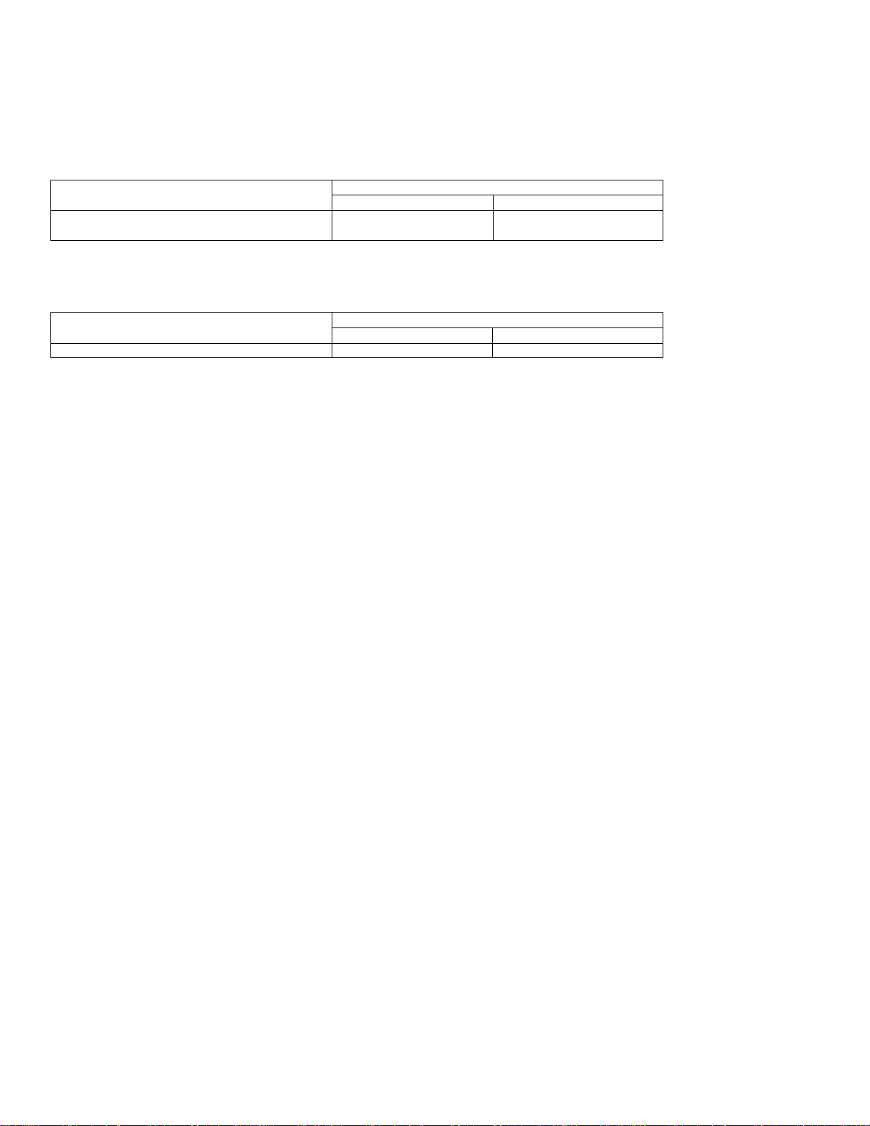
6 DISC IN-DASH CD CHANGER
CDX-MG6167
ZH ES
HONDA
VEHICLE DESTINATION PRODUCED AFTER PART No. ID No. PIONEER MODEL No.
INTEGRA Australia July 2001 08A06-3D7-300 CDX-MG6167ZH/ES
- This service manual should be used together with the manual(s) listed below.
For the parts numbers, adjustments, etc. which are not shown in this manual, refer to the following
manual(s).
Model Order No. Mech. Module Remarks
CDX-MG6346ZH/ES CRT2407
CX-890 CRT2376 G1
CD Mechanism Module:Circuit Description, Mechanism Operation, Disassembly
Page 2
CDX-MG6167ZH
EXPLODED VIEWS AND PARTS LIST
PACKING (Page 3)
- PACKING SECTION PARTS LIST
Part No.
Mark No. Description CDX-MG6346ZH/ES CDX-MG6167ZH/ES
11 Carton CHG4457 CHG4514
12 Contain Box CHL4457 CHL4514
EXTERIOR (Page 4)
- EXTERIOR SECTION PARTS LIST
Part No.
Mark No. Description CDX-MG6346ZH/ES CDX-MG6167ZH/ES
41 Grille Unit CXB8378 CXB8264
Page 3
PIONEER CORPORATION 4-1, Meguro 1-Chome, Meguro-ku, Tokyo 153-8654, Japan
PIONEER ELECTRONICS SERVICE INC. P.O.Box 1760, Long Beach, CA 90801-1760 U.S.A.
PIONEER ELECTRONIC [EUROPE] N.V. Haven 1087 Keetberglaan 1, 9120 Melsele, Belgium
PIONEER ELECTRONICS ASIACENTRE PTE.LTD. 253 Alexandra Road, #04-01, Singapore 159936
C PIONEER CORPORATION 1999
K-ZZB. OCT. 1999 Printed in Japan
ORDER NO.
CRT2407
6 DISC IN-DASH CD CHANGER
6 DISC IN-DASH CD CHANGER
CDX-MG6346ZH ES
HONDA
CONTENTS
1. SAFETY INFORMATION ............................................2
2. EXPLODED VIEWS AND PARTS LIST.......................3
3. BLOCK DIAGRAM AND SCHEMATIC DIAGRAM...10
4. PCB CONNECTION DIAGRAM ................................26
5. ELECTRICAL PARTS LIST ........................................42
6. ADJUSTMENT..........................................................46
7. GENERAL INFORMATION .......................................48
7.1 DIAGNOSIS ........................................................48
7.1.1 TEST MODE..............................................48
7.1.2 DISASSEMBLY .........................................52
7.1.3 CONNECTOR FUNCTION DESCRIPTION.......56
7.2 IC ........................................................................57
8. OPERATIONS AND SPECIFICATIONS.....................61
VEHICLE DESTINATION PRODUCED AFTER HONDA PART No. ID No. PIONEER MODEL No.
Not specified THAILAND, AUSTRALIA October 1999 08A06-3B5-300 CDX-MG6346ZH/ES
Not specified THAILAND, AUSTRALIA October 1999 08A06-3B5-310 CDX-MG6446ZH/ES
- This service manual should be used together with the following manual(s):
Model No. Order No. Mech. Module Remarks
CX-890 CRT2376 G1 CD Mechanism Module:Circuit Description, Mechanism Operation, Disassembly
CDX-MG6446ZH ES
CDX-MG6346ZH/ES
Page 4
2
CDX-MG6346ZH,MG6446ZH
- CD Player Service Precautions
1. For pickup unit(CXX1311) handling, please refer
to"Disassembly"(see page 52).
During replacement, handling precautions shall be
taken to prevent an electrostatic discharge(protection
by a short pin).
2. During disassembly, be sure to turn the power off
since an internal IC might be destroyed when a connector is plugged or unplugged.
3. Please checking the grating after changing the service pickup unit(see page 46).
- When the Repair is Complete
When the repair is complete, make the CD mechanism
ready for transportation implementing the following
procedures:
1. Press the changer side 1 and 4 simultaneously to turn
the ACC on.
2. As the ACC is turned on, the disc indicator blinks in
red.
3. When the blinking is stopped, the mechanism is
ready for the transportation.
4. Attach the Transportation Bracket (CNC7878). Now
you can transport it.(See the figure below)
This service manual is intended for qualified service technicians; it is not meant for the casual do-it-yourselfer.
Qualified technicians have the necessary test equipment and tools, and have been trained to properly and safely repair
complex products such as those covered by this manual.
Improperly performed repairs can adversely affect the safety and reliability of the product and may void the warranty.
If you are not qualified to perform the repair of this product properly and safely; you should not risk trying to do so
and refer the repair to a qualified service technician.
1. SAFETY INFORMATION
Transportation Bracket
(CNC7878)
Case
(CNB2354)
Page 5
CDX-MG6346ZH,MG6446ZH
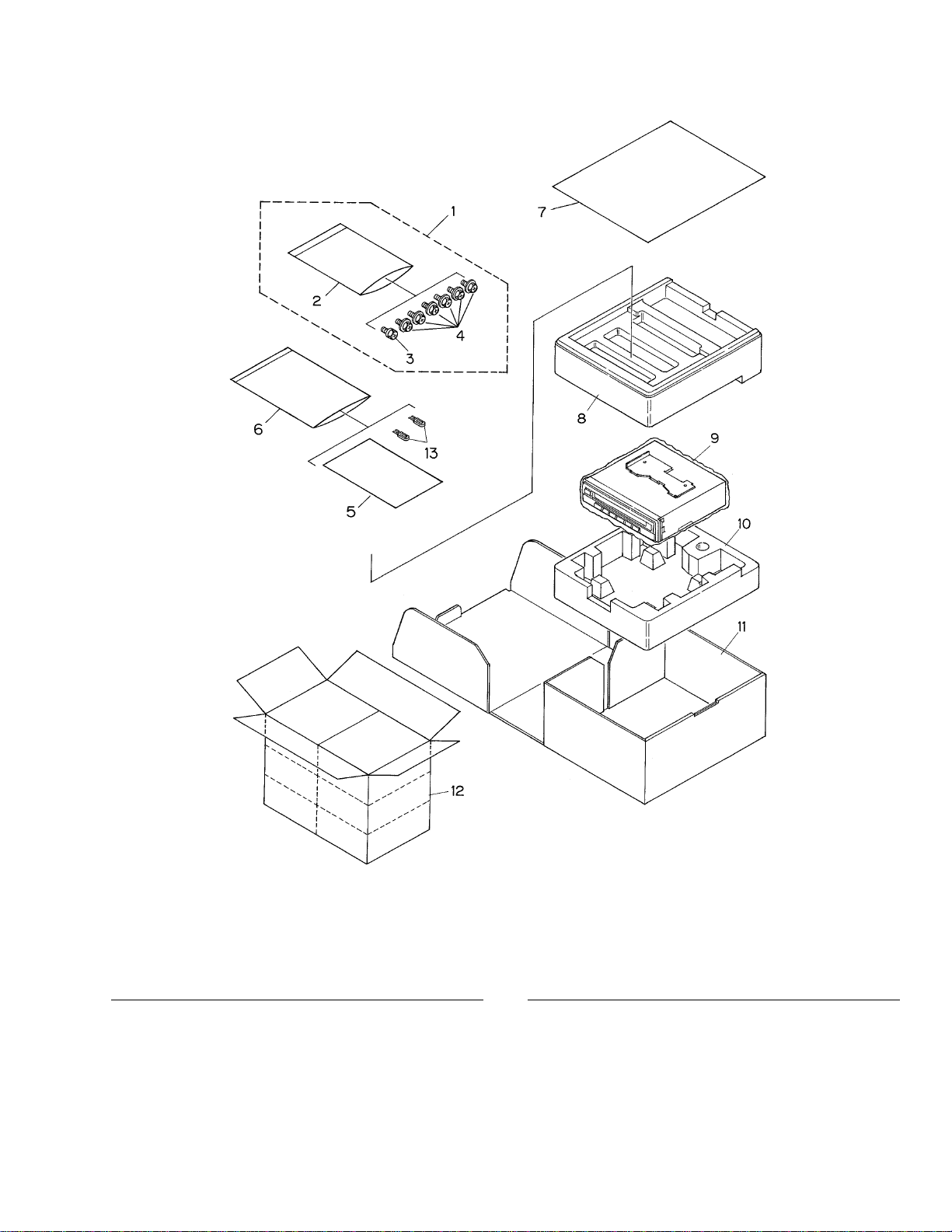
1 Screw Assy CEA2537
* 2 Polyethylene Bag CEG-127
3 Screw HMF40P060FZK
4 Screw HMF50P080FMC
5 Owner’s Manual(English) CRB1561
6 Polyethylene Bag CEG1116
* 7 Sheet CHW1402
8 Protector CHP2123
* 9 Polyethylene Bag E36-609
10 Protector CHP2124
11 Carton
(CDX-MG6346ZH/ES) CHG3909
Carton
(CDX-MG6446ZH/ES) CHG3991
12 Contain Box
(CDX-MG6346ZH/ES) CHL3909
Contain Box
(CDX-MG6446ZH/ES) CHL3991
* 13 Band CNF-512
Mark No. Description Part No. Mark No. Description Part No.
- PACKING SECTION PARTS LIST
NOTE:
- Parts marked by “*” are generally unavailable because they are not in our Master Spare Parts List.
- Screws adjacent to
∇ mark on the product are used for disassembly.
2. EXPLODED VIEWS AND PARTS LIST
2.1 PACKING
3
Page 6
4
CDX-MG6346ZH,MG6446ZH
2.2 EXTERIOR
Page 7

CDX-MG6346ZH,MG6446ZH
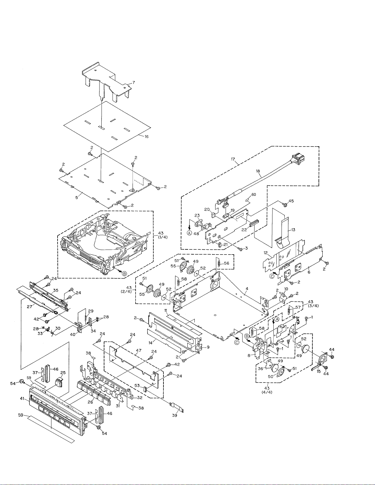
1 Screw BMZ20P020FMC
2 Screw BMZ26P030FMC
3 Screw BMZ26P060FMC
4 Chassis Unit
(CDX-MG6346ZH/ES) CXB3407
Chassis Unit
(CDX-MG6446ZH/ES) CXB5581
5 Case CNB2354
6 Side Frame CNB2397
7 Bracket CNC7878
8 Bracket
(CDX-MG6346ZH/ES) CNC8026
Bracket
(CDX-MG6446ZH/ES) CNC8816
9 Front Frame CNC8110
10 Holder CNC8111
11 Insulator CNM5969
12 Insulator CNM6112
13 PCB CNP5516
14 Insulator CNM6409
15 Holder CNV5543
* 16 Caution Label CRP1200
17 Extension Unit CWM6677
18 Cord CDE6148
19 Connector(CN102) CKS2200
20 Connector(CN103) CKS3597
21 Connector(CN701) CKS3785
22 Connector(CN101) CKS3989
23 Holder CNC8031
24 Screw BPZ20P060FMC
25 Button CAC5864
26 Button CAC5865
27 Door CAT2003
28 Washer CBF1038
29 Spring CBH2201
30 Spring CBH2200
31 Conductor CNC8051
32 Lighting Conductor CNV5901
33 Gear CNV5547
34 Arm CNV5548
35 Guide CNV5880
36 Sheet CNM6318
37 Double Faced Tape CNM6424
38 Insulator CNM6512
39 PCB CNP5373
40 Bracket Unit CXB3111
41 Grille Unit CXB3409
42 Screw IMS20P040FMC
43
CD Mechanism Module(G1) CXK4702
44 Screw IMS20P040FMC
45 Screw IMS26P040FMC
46 Cushion CNV5674
47 Keyboard Unit CWM6289
48 Transistor(Q708) 2SB1335A
49 Damper CNV5120
50 Holder CNC7826
51 Screw CBA1250
52 Sheet CNM5981
53 Connector(CN901) CKS3785
54 Screw IMS26P030FZK
55 Holder CNC7477
56 Spring(Left Rear) CBH2365
57 Spring(Right Rear)(Black) CBH2361
58 Spring(Front) CBH2360
59 Spacer CNM6658
60 Spacer CNM6626
- EXTERIOR SECTION PARTS LIST
Mark No. Description Part No.
Mark No. Description Part No.
5
Page 8
6
CDX-MG6346ZH,MG6446ZH
2.3 CD MECHANISM
Page 9

7
CDX-MG6346ZH,MG6446ZH
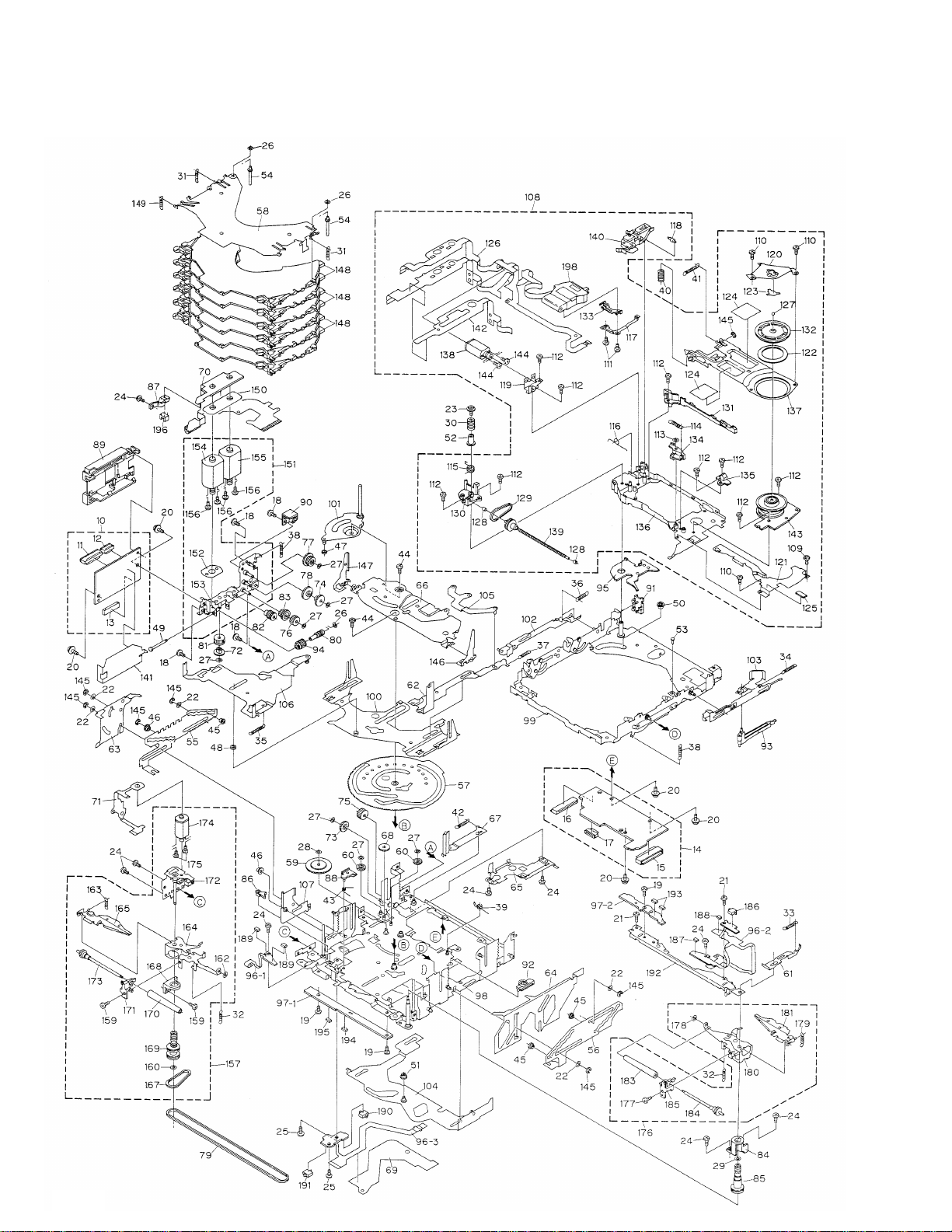
1-9 •••••
10 CD Core Unit(Servo Unit) CWX2202
11 Connector(CN101) CKS2764
12 Connector(CN301) CKS3966
13 Connector(CN201) CKS3991
14 CD Core Unit(STS Unit) CWX2203
15 Connector(CN701) CKS3989
16 Connector(CN801) CKS3989
17 Connector(CN802) CKS4054
18 Screw CBA1037
19 Screw CBA1041
20 Screw CBA1076
21 Screw CBA1250
22 Screw CBA1405
23 Screw CBA1452
24 Screw CBA1453
25 Screw CBA1479
26 Washer CBF1037
27 Washer CBF1038
28 Washer CBF1039
29 Washer CBF1064
30 Spring CBH2007
31 Spring CBH2271
32 Spring CBH2274
33 Spring CBH2014
34 Spring CBH2015
35 Spring CBH2016
36 Spring CBH2017
37 Spring CBH2290
38 Spring CBH2019
39 Spring CBH2064
40 Spring CBH2195
41 Spring CBH2196
42 Spring CBH2224
43 Spring CBH2250
44 Screw CBA1082
45 Roller CLA3154
46 Roller CLA3157
47 Roller CLA3159
48 Roller CLA3160
49 Shaft CLA3179
50 Spacer CLA3194
51 Roller CLA3248
52 Bush CLA3353
* 53 Shaft CLA3469
54 Shaft CLA3693
55 Steer CNC7215
56 Steer CNC7216
57 Cam CNC7227
* 58 Holder CNC7235
59 Gear CNC7236
60 Gear CNC7238
61 Lever CNC7243
62 Lever CNC7244
63 Lever CNC7245
64 Lever CNC7246
65 Cover CNC7441
66 Holder CNC8613
67 Lever CNC8024
68 Gear CNC8140
69 Sheet CNM5831
70 PCB CNP5680
71 PCB CNP5681
72 Gear CNR1479
73 Gear CNR1481
74 Gear CNR1495
75 Gear CNR1501
76 Gear CNR1502
77 Gear CNR1540
78 Gear CNR1541
79 Belt CNT1080
80 Worm Gear CNV5046
81 Gear CNV5047
82 Gear CNV5048
83 Gear CNV5049
84 Holder CNV5056
85 Pulley CNV5058
86 Arm CNV5061
87 Spacer CNV5066
88 Arm CNV5189
89 Cover CNV5207
90 Cover CNV5424
91 Cover CNV5425
92 Lever CNV5427
93 Arm CNV5491
94 Gear CNV5519
95 Holder CNV5648
96 Composite PCB CNX3141
97 Composite PCB CNX2989
98 Chassis Unit CXB4314
- CD MECHANISM SECTION PARTS LIST
Mark No. Description Part No.
Mark No. Description Part No.
Page 10

8
CDX-MG6346ZH,MG6446ZH
99 Frame Unit CXB2702
100 Lever Unit CXB2703
101 Arm Unit CXB2704
102 Lever Unit CXB2708
103 Lever Unit CXB2709
104 Lever Unit CXB2711
105 Arm Unit CXB2712
106 Lever Unit CXB2713
107 Lever Unit CXB2714
108
Carriage Mechanism Unit(G1) CXB5639
109 Screw CBA1041
110 Screw CBA1250
111 Screw CBA1362
112 Screw CBA1471
113 Washer CBF1038
114 Spring CBH2008
115 Spring CBH2009
116 Spring CBH2010
117 Spring CBL1335
118 Roller CLA3707
* 119 Bracket CNC7228
120 Guide Unit CXB4417
121 Cover CNC7628
122 Sheet CNM6414
123 Sheet CNM5378
124 Sheet CNM5695
125 Sheet CNM5827
126 PCB CNP4978
127 Ball CNR1189
128 Bearing CNR1423
129 Belt CNT1079
130 Holder CNV5037
131 Guide CNV5040
132 Clamper CNV5042
133 Rack CNV5111
134 Arm CNV5579
135 Holder CNV5759
* 136 Chassis CXB2698
137 Arm Unit CXB2705
138
Motor Unit(M4 CARRIAGE) CXB3178
139 Screw Unit CXB3179
140 Lever Unit CXB4450
141 Insulator CNM6306
142 Spacer CNM6345
143 Motor(M5 SPINDLE) CXM1120
144 Screw JFZ14P020FZK
145 Washer YE15FUC
146 Arm Unit CXB4953
147 Arm Unit CXB4954
148 Tray Assy CXB4307
149 Spring CBH2269
150 Sheet CNM6699
151 Cam Motor Assy CXB3170
152 Spacer CNC8289
* 153 Bracket Unit CXB4165
* 154
Motor Unit(M1 Cam Gear) CXB3174
* 155 Motor Unit(M3 ELV) CXB3175
156 Screw JFZ20P025FMC
157 Loading Arm L Assy CXB3171
158 •••••
159 Screw CBA1453
160 Washer CBF1038
161 •••••
162 Washer CBF1074
163 Spring CBH2136
* 164 Arm CNC7241
* 165 Arm CXB4449
166 •••••
167 Belt CNT1079
168 Holder CNV5055
169 Pulley CNV5057
170 Roller CNV5064
171 Guide CNV5125
* 172 Bracket Unit CXB4316
173 Roller Gear Unit CXB3176
* 174 Motor Unit(M2 LOAD) CXB3177
175 Screw JFZ14P020FMC
176 Loading Arm R Assy CXB3172
177 Screw CBA1453
178 Washer CBF1074
179 Spring CBH2136
* 180 Arm CNC7242
* 181 Arm CXB4448
182 •••••
183 Roller CNV5064
184 Roller Gear Unit CXB3176
185 Guide CNV5126
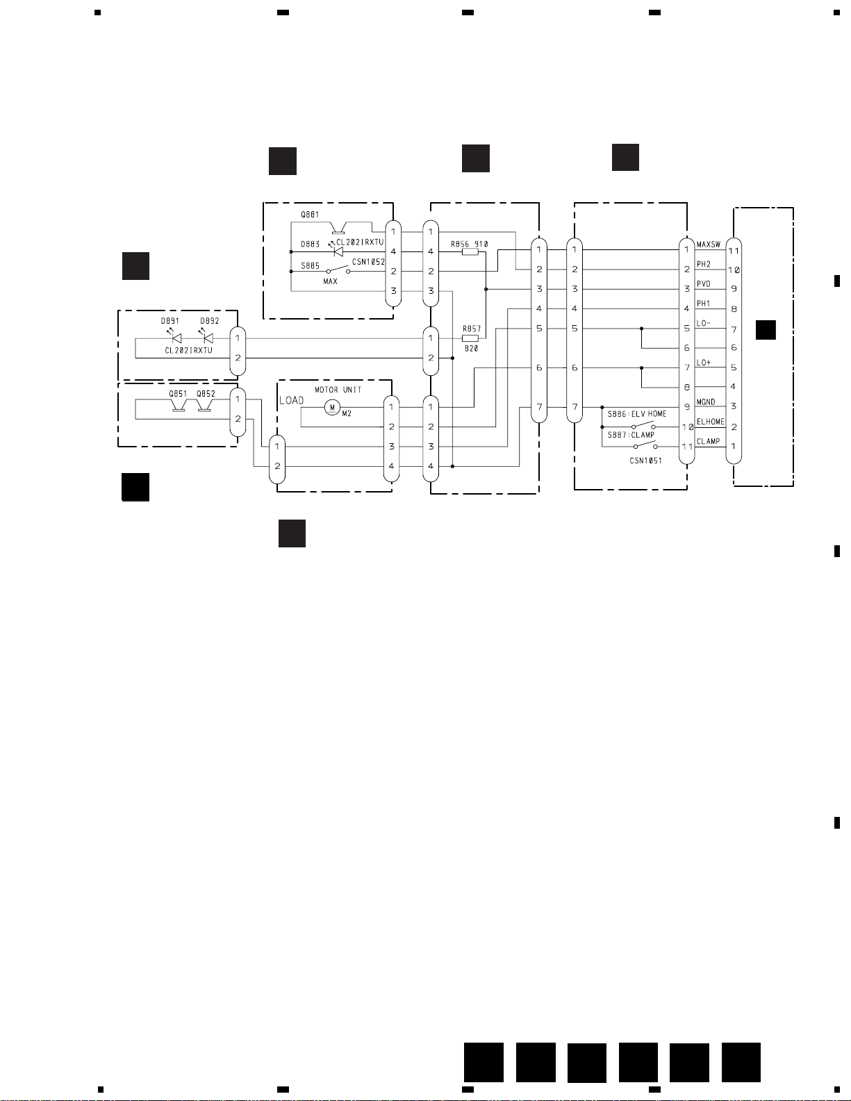
186 Switch(S885 MAX) CSN1052
187 LED(D883) CL202IRXTU
188 Photo-transistor(Q881) CPT230SCTD(CD)
Mark No. Description Part No.
Mark No. Description Part No.
Page 11

9
CDX-MG6346ZH,MG6446ZH
Mark No. Description Part No.
189 LED(D891,892) CL202IRXTU
190 Switch(S887 CLAMP) CSN1051
191 Switch(S886 ELV HOME) CSN1052
192 Bracket Unit CXB4306
193
Photo-transistor(Q851,852) CPT230SCTD(CD)
194 Resistor(R856) RS1/8S911J
195 Resistor(R857) RS1/8S821J
196 Photo-interrupter(Q1) RPI-221
197 •••••
198 Pickup Unit(Service)(P8) CXX1311
Page 12
10
CDX-MG6346ZH,MG6446ZH
1
23
4
1234
D
C
B
A
PICKUP UNIT(SERVICE)
MOTOR PCB(B)
MOTOR PCB(A)
CD CORE UNIT(SERVO UNIT)
PCB UNIT(D)
PCB UNIT(A)
PCB UNIT(C)
PCB UNIT(E)
PCB UNIT(B)
LOAD MOTOR PCB
CD CORE UNI
HOLOGRAM
UNIT
FOCUS ACT
TRACKING ACT
MD
LD+
LD-
LD
MD
FO+
TO+
16
17
V5
Q101
Q102
PD
LD
CN101
IC101
UPC2572GS
RF AMP
IC201
UPD63702AGF
DIGITAL SERVO
PROCESSOR
DIGITAL SIGNAL
PROCESSOR
µ-COMPUTER
INTERFACE
35
69
EFM
CD 4CH DRIVER
IC301
BA5986FM
14
11
16
15
22
BVD
V5
MUTE
9
MD/SD/TD/FD
74
10
11
VR2
XTAL
XTAL
X201
5V
VD
CONT
CN201 CN801
5V
VD
CN301
WDCK
RFCK
RAOV
LRCK
SCKO
DOUT
MCK
IC501
CXD2511R
SHOCKPROOF
CONTROL
B
DA
LR
X
IC502
MSM514400DP-60TS
4M DRAM
V+5V
IC701
BA05S
5V REGULA
VM
4
1
XAO/XSTB/XSO/XS
MOTOR DRIVER
IC802
LB1836M
2
6
3
5
ELVSNS
MOTOR DRIVER
LB1836M
IC801
2
6
13
9
5
3
12
10
CGCG+
ELEL+
PVD
LOLO+
PVD
PVD
Q80
Q802
CLAMP
ELHOME
CN802
M
BCL
SPINDLE
MOTOR
CARRIAGE
MOTOR
HOME
SWITCH
EC
VM
VCC
ST/SR
GND
HOME
M
LOADING
MOTOR
M
CAMGEAR
MOTOR
M
ELEVATION
MOTOR
Q851
Q852
D891
D892
PH1
PVD
Q881
D883
PH2
S883
MAX
SWITCH
PH1
PVD
PH1
PH2
MAXSW
LD MOTOR-
LD MOTOR+
MAXSW
PH2
PH1
PVD
ELV HOME
S886
S887
CLAMP
ELEVATION
SENSE
KEYB
KEY MATRIX
D905~916
5
14
15
4
3
1
2
3
4
8
5
6
7
10
11
1
1
1
1
2
3
4
1
2
4
1
2
1
1
2
3
5
6
3
4
2
1
5
6
3
4
2
1
5
7
3
4
2
1
7
5
9
8
10
11
10
2
11
1
19
28
29
30
19
28
29
30
45
44
46
36
35
37
32
33
39
41
41
43
48
50
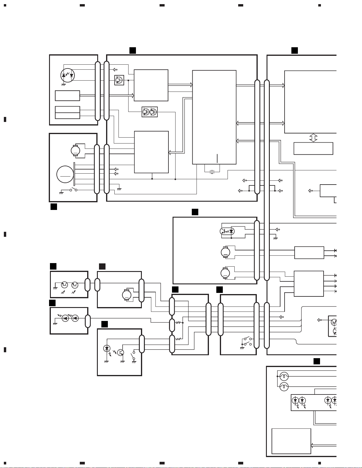
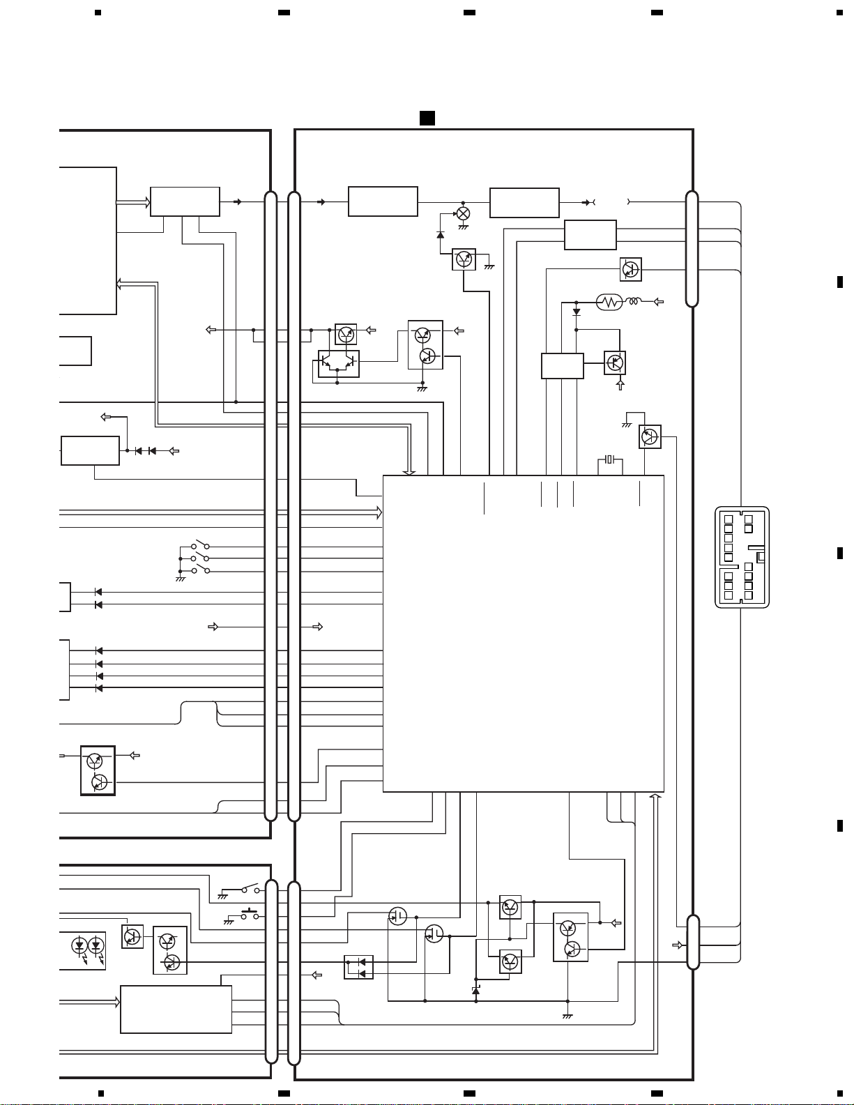
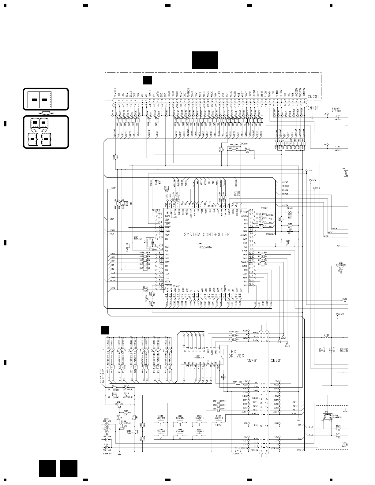
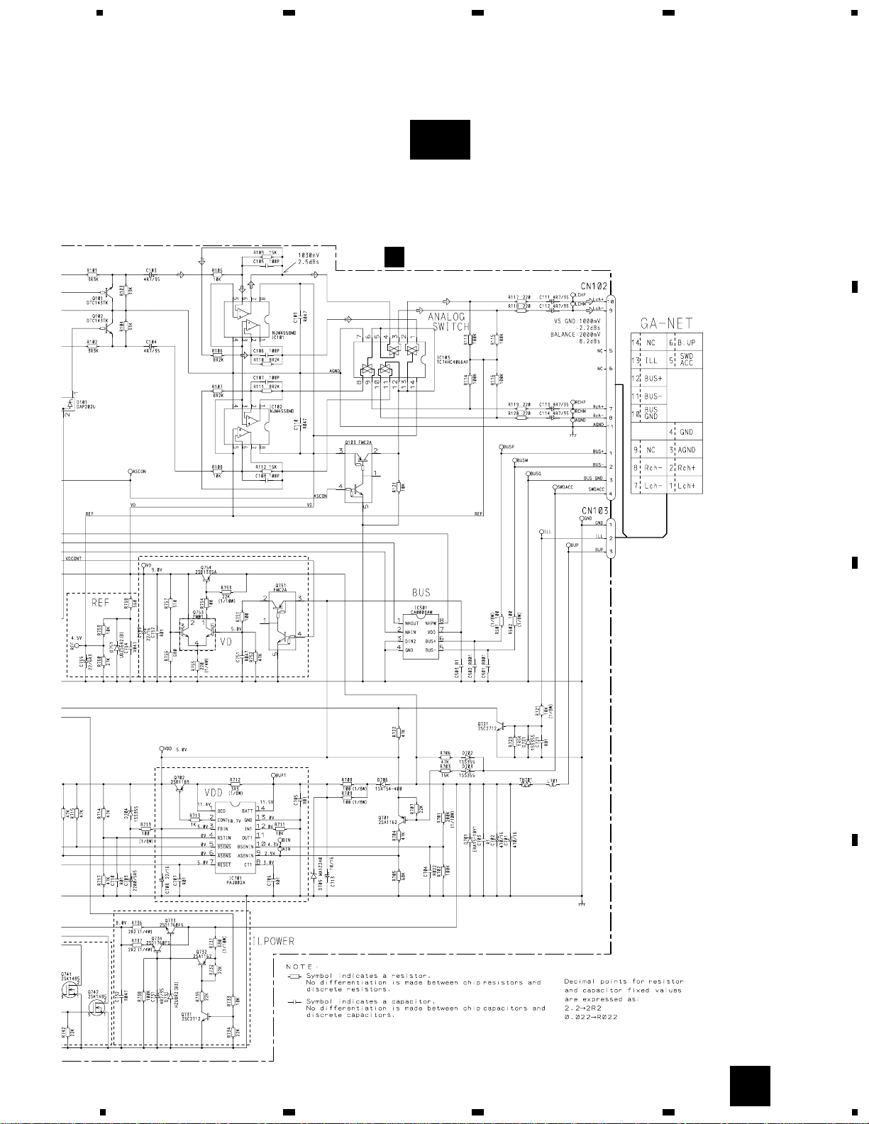
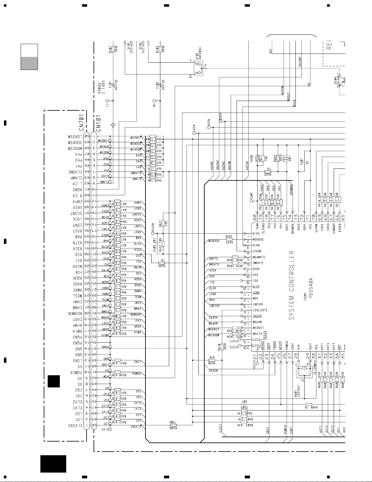
3. BLOCK DIAGRAM AND SCHEMATIC DIAGRAM
3.1 BLOCK DIAGRAM
K
G
L
J
I
H
F
E
C D
B
Page 13
11
CDX-MG6346ZH,MG6446ZH
5
6
78
5
6
78
D
C
B
A
BCK
DATA
LRCK
XTLI
39
512
IC601
AK4321VF
8fs DF D/A LPF
CN701
CN101
6
18
DEMO
PD
VD
VD
LCH
WDSL/CHMO/CHMI
XWRE/XRDE/XQOK
XWIH/XEMP/ADRMON/CHDT
IC701
BA05SFP
REGULATOR
VM
VD
POWER
CONT
EMPH
2
1
TB/XSO/XSI/XSCK/XRST/SCONT
ELVSNS
LOADSW
DOORSW
MODESW
S801
S802
S803
2
6
2
6
13
9
CG1
CG2
ELV1
ELV2
LO1
LO2
MAXSW
PH2
PH1
Q801
VD
LOAD
LOAD
ELHOME
CLAMP
ELVSNS
V+5V
V+5V
KEYBOARD UNIT
EXTENSION UNIT
NJM4558MD
IC101
LPF
VD REGULATOR
VDD
B.U
B.U
WDSL/CHM0/CHM1
XWRE/XRDE/XQOK
XWIH/XEMP/ADRMON
CHDT
PD5540A
SYSTEM
CONTROLLER
IC601
ILL POWER
CD MUTE
CN102
LCH
6
7
53
27
13
56
4
16
15 22
28
29
Q101
Q104
CD-LCH
BUS+
ASENS
VDCONT
Q751
Q754
X601
Q701
Q702
SWDACC
NHOUT
NHPOW
Q753
XOUT
XIN
BSENS
ASENS
CDMUTE
VDCONT
CONT
EMPH
EXMODE
POWER
LOADSW
DOORSW
ELVSW
CG1
CG2
ELV1
ELV2
LO1
LO2
PH3
PH2
PH1
LOAD
ELHOME
CLAMPSW
26
79
17
2
18
62
61
60
59
58
57
78
77
76
55
6
5
DCLOSE
EJECTKEY
ILL1
ILL2
ILPOW
EXSO
EXCSK
DATA
EXCK
401436 37
70
686667
Q741
Q733
Q732
B.U
Q731
Q734
Q742
GND
CN701
CN901
CN103
KEY DATA
DOORSW
DOORSW
ILPOWILPOW
EJECT
EJECT
ILL1
ILL1
ILL2
ILL2
ILL
ILL
VDD
VDD
DATA
CLK
MODE
LED DRIVER
IC901
BU2092FV
Q904
Q903
Q905
16
20
2
3
4
GA-NET
14P
42
8
9
9
43
42
35 16
39
12
10 41
1
50
49
48
50
1
2
3
6
7
45
44
11 40
4
47
5
46
2
49
3
48
47
46
45
4
5
6
12 39
44
7
43
8
16
12
7
14
15
17
13
10
8
9
9
10
8
5
1
3
4
11
6
2
1
3
4
2
9
TC74HC4066AF
IC103
ANALOG SWITCH
NHPOW
NHOUT
CA0008AM
IC501
BUS
BUS-
1
6
5
1
8
VD
PAJ002A
IC701
VDD
25
RESET
6
5
7
91014
2
B.U
Q721
ISENS
24
2
ILL
4
3
VDD
ILL
A
Page 14
12
CDX-MG6346ZH,MG6446ZH
1
23
4
1234
D
C
B
A
A
3.2 OVERALL CONNECTION DIAGRAM(GUIDE PAGE)
Note: When ordering service parts, be sure to refer to “EXPLODED VIEWS AND PARTS LIST” or “ELECTRICAL PARTS
LIST”.
A-a A-b
A-a
A-b
A-b
A-a
Large size
SCH diagram
Guide page
Detailed page
B
A-a
D
CD CORE UNIT(STS UNIT)
B
KEYBOARD UNIT
Page 15
13
CDX-MG6346ZH,MG6446ZH
5
6
78
5
6
78
D
C
B
A
A
A-b
A
EXTENSION UNIT
Page 16
14
CDX-MG6346ZH,MG6446ZH
1
23
4
1234
D
C
B
A
1
A-a
A-b
D
CD CORE UNIT(STS UNIT)
A-a
Page 17
15
CDX-MG6346ZH,MG6446ZH
5
6
78
5
6
78
D
C
B
A
A-a
A-b
B
2
B
KEYBOARD UNIT
A-a
Page 18

16
CDX-MG6346ZH,MG6446ZH
1
23
4
1234
D
C
B
A
A-a
A-b
1
A
EXTENSION UNIT
A-b
Page 19
17
CDX-MG6346ZH,MG6446ZH
5
6
78
5
6
78
D
C
B
A
A-a
A-b
2
A-b
Page 20
(SERVICE)
M5 SPINDLE
CXM1120
DISC INSERT DETECT
M4 CARRIAGE
CXB3178
2.5V
RF AMP/
AUTO POWER
CONTROL
CD DRIVER
D
E
MOTOR PCB(B)
CD CORE UNIT(SERVO UNIT)
18
CDX-MG6346ZH,MG6446ZH
1
23
4
1234
D
C
B
A
C
E
C
3.2 CD CORE UNIT(SERVO UNIT)
Page 21
16.934MHz
22/6R3
FOCUS/TRACKING
CARRIAGE/SPINDLE
DIGITAL SERVO
DIGITAL SIGNAL PROCESSOR
D/A CONVERTER
F
19
CDX-MG6346ZH,MG6446ZH
5
6
78
5
6
78
D
C
B
A
C
Page 22
M1 : CXB3174
Q1 : RPI-221
M3 : CXB3175
SURE TRACK
MEMORY CONTRO
+5V REGULATOR
7.5V
9.0V
MOTOR DRIVER
G
F
D
H
LOAD SWITCH
DOOR SWITCH
MODE SWITCH
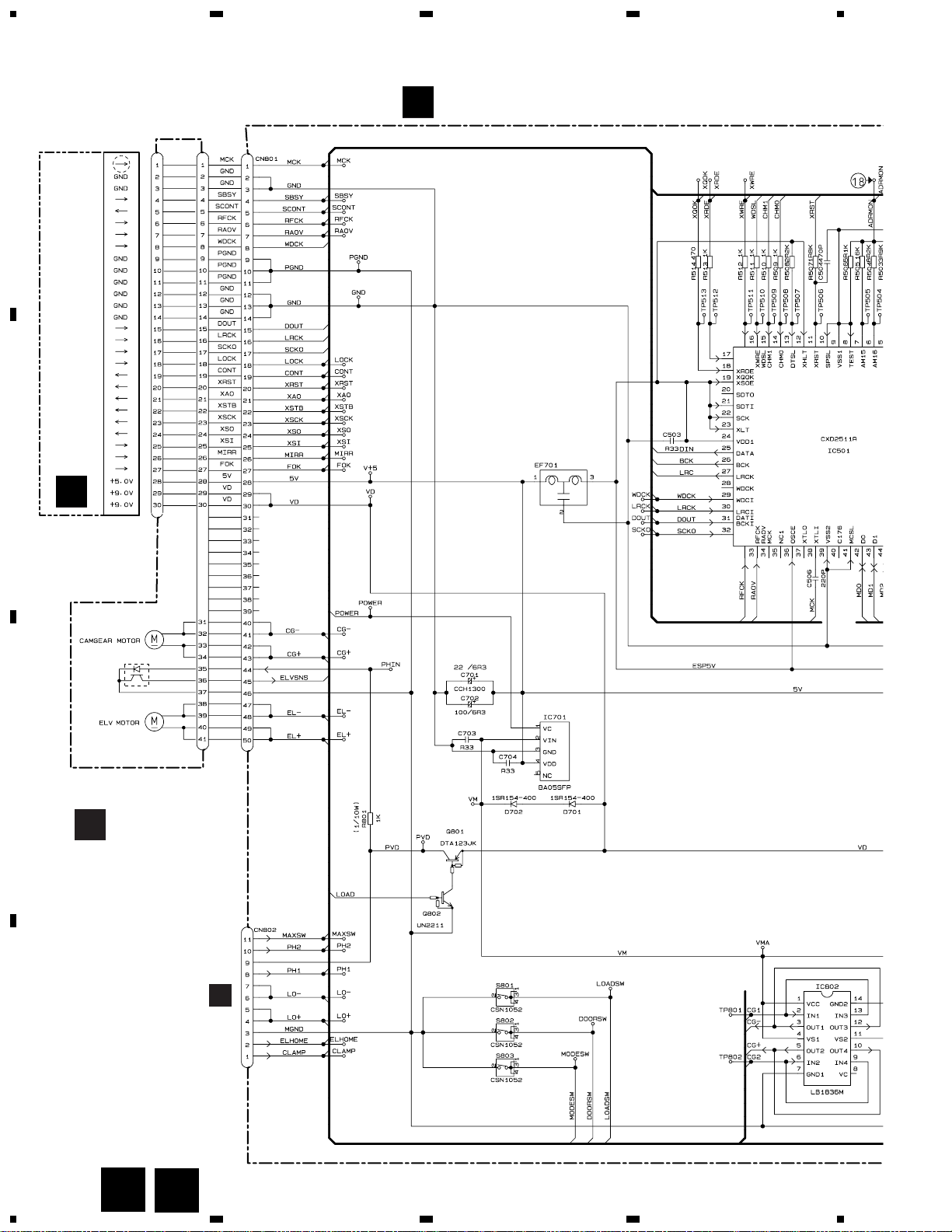
CD CORE UNIT(STS UNIT)
CD CORE UNIT
(SERVO UNIT)
MOTOR PCB
(A)
ELV SENSE
20
CDX-MG6346ZH,MG6446ZH
1
23
4
1234
D
C
B
A
D
F
C
D
3.3 CD CORE UNIT(STS UNIT)
Page 23
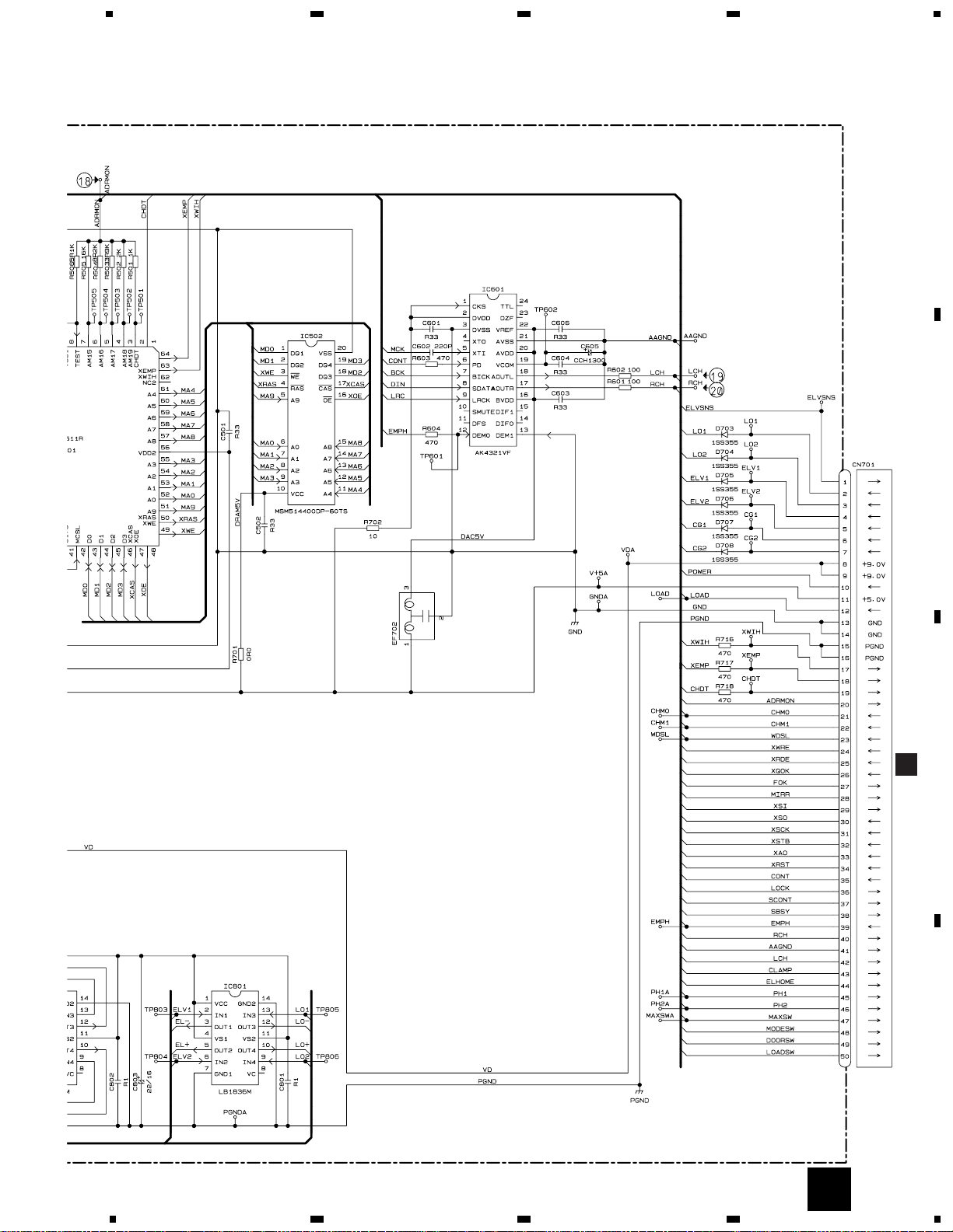
22/6R3
RY CONTROLLER
MOTOR DRIVER
4M DRAM
D/A CONVERTER
A
CN101
21
CDX-MG6346ZH,MG6446ZH
5
6
78
5
6
78
D
C
B
A
D
Page 24
22
CDX-MG6346ZH,MG6446ZH
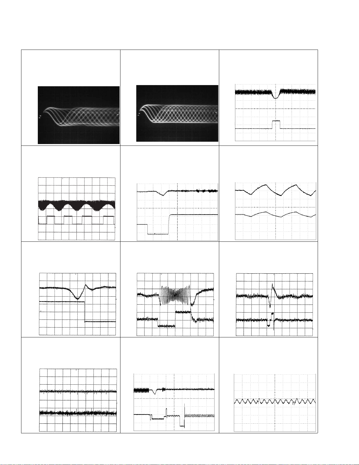
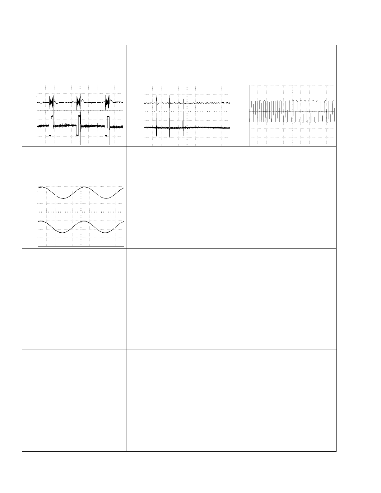
1 RFO 0.5V/div. 0.2µs/div.
Normal mode: play
1 CH1: RFO 1V/div.
2 CH2: MIRR 5V/div.
Test mode: Tracking open
0.5ms/div.
1 CH1: RFO 1V/div.
2 CH2: MIRR 5V/div.
Normal mode: The defect part
passes 500µs/div.
0.5ms/div.
3 CH1: FIN 0.5V/div.
4 CH2: FOP 2V/div.
Test mode: No disc, Focus close
0.2s/div.
3 CH1: FIN 0.5V/div.
5 CH2: FOK 2V/div.
Normal mode: Focus close
0.2s/div.
6 CH1: FEY 0.5V/div.
7 CH2: XSI 2V/div.
Normal mode: Focus close
1ms/div.
8 CH1: TEY 0.5V/div.
9 CH2: TIN 0.5V/div.
Test mode: 32 tracks jump (FWD)
0.5ms/div.
8 CH1: TEY 0.5V/div.
9 CH2: TIN 0.5V/div.
Test mode: Single jump (FWD)
0.5ms/div.
6 CH1: FEY 0.1V/div.
3 CH2: FIN 0.2V/div.
Normal mode: Play
20ms/div.
3 CH1: FIN 0.5V/div.
0 CH2: SIN 1V/div.
Normal mode: Focus close
0.5s/div.
GND
→
GND
→
GND
→
GND
→
- Waveforms
0 SIN 0.5V/div. 0.1s/div.
Normal mode: Play
REFOUT
→
REFOUT
→
REFOUT
→
REFOUT
→
REFOUT
→
REFOUT
→
REFOUT
→
REFOUT
→
REFOUT
→
REFOUT
→
REFOUT
→
REFOUT
→
REFOUT
→
REFOUT
→
REFOUT
→
REFOUT
→
1 RFO 0.5V/div. 0.5µs/div.
Test mode
REFOUT
→
REFOUT
→
REFOUT
→
Note:1. The encircled numbers denote measuring pointes in the circuit diagram.
2. Reference voltage
REFOUT:2.5V
Page 25
23
CDX-MG6346ZH,MG6446ZH
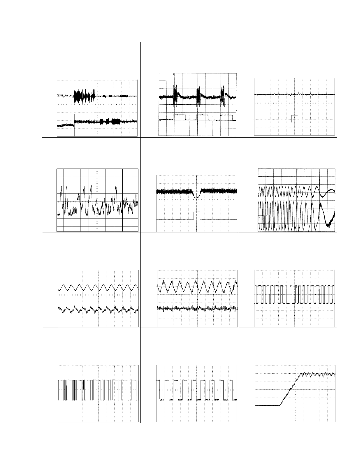
3 CH1: FIN 1V/div.
$ CH2: HOLD 5V/div.
Normal mode:
The defect part passes 800µm
8 CH1: TEY 0.5V/div.
6 CH2: FEY 0.1V/div.
Normal mode: AGC after focus close
8 CH1: TEY 0.5V/div.
! CH2: SD 0.5V/div.
5ms/div.
0 SIN 1V/div. 10ms/div.
Long Search
8 CH1: TEY 1V/div.
# CH2: TEC 1V/div.
Test mode: Focus close
Tracking open
2ms/div.
6 CH1: FEY 0.2V/div.
3 CH2: FIN 0.5V/div.
Normal mode: During
AGC
1ms/div.
@ EFM 1V/div. 2µs/div.
Play
0.2s/div.
% Dout 2V/div. 5µs/div.
Play
^ LRCK 2V/div. 10µs/div. * ADRMON 1V/div. 1s/div.
Normal mode: Starting play
GND
→
REFOUT
→
REFOUT
→
REFOUT
→
REFOUT
→
REFOUT
→
REFOUT
→
REFOUT
→
REFOUT
→
REFOUT
→
REFOUT
→
REFOUT
→
REFOUT
→
REFOUT
→
REFOUT
→
1 CH1: RFO 1V/div.
$ CH2: HOLD 5V/div.
Normal mode:
The defect part passes 800µm
500µs/div.
REFOUT
→
REFOUT
→
8 CH1: TEY 0.2V/div.
9 CH2: TIN 0.5V/div.
Normal mode: During
AGC
1ms/div.
REFOUT
→
REFOUT
→
GND
→
GND
→
500µs/div.
Page 26
24
CDX-MG6346ZH,MG6446ZH
8 CH1: TEY 0.5V/div.
9 CH2: TIN 0.5V/div.
Test mode: 100 tracks jump(FWD)
8 CH1: TEY 0.5V/div.
9 CH2: TIN 0.5V/div.
Normal mode: Play
10ms/div.
5ms/div.
REFOUT
→
REFOUT
→
& SCKO 2V/div. 500ns/div.
Play
REFOUT
→
) CH1: RCH 2V/div.
( CH2: LCH 2V/div.
Normal mode: PLAY (0dB,1kHz)
200µs/div.
AAGND
→
AAGND
→
REFOUT
→
REFOUT
→
Page 27
H
I
J
L
M
K
CXB3177
G
CN802
SWITCH
PCB UNIT(A)
PCB UNIT(C)
PCB UNIT(E)
PCB UNIT(B)
PCB UNIT(D)
LOAD MOTOR PCB
CPT230SCTD(CD)
CPT230SCTD(CD)
25
CDX-MG6346ZH,MG6446ZH
1
2
34
1
2
34
D
C
B
A
3.4 PCB UNIT(A,B,C,D,E), LOAD MOTOR PCB
L
I
H
G
J
K
G
D
Page 28
26
CDX-MG6346ZH,MG6446ZH
1
23
4
1234
D
C
B
A
NOTE FOR PCB DIAGRAMS
1. The parts mounted on this PCB
include all necessary parts for
several destination.
For further information for
respective destinations, be sure
to check with the schematic diagram.
2. Viewpoint of PCB diagrams
EXTENSION UNIT
4. PCB CONNECTION DIAGRAM
4.1 EXTENSION UNIT
Capacitor
Connector
P.C.Board
Chip Part
SIDE A
SIDE B
SIDE A
CORD
A
A
Page 29

27
CDX-MG6346ZH,MG6446ZH
1
2
34
1
2
34
D
C
B
A
CN701
CN901
EXTENSION UNIT
SIDE B
A
A
B
D
Page 30

28
CDX-MG6346ZH,MG6446ZH
1
23
4
1234
D
C
B
A
4.2 KEYBOARD UNIT
KEYBOARD UNIT
CN701
SIDE A
B
B
A
Page 31

29
CDX-MG6346ZH,MG6446ZH
1
2
34
1
2
34
D
C
B
A
SIDE B
KEYBOARD UNIT
B
B
Page 32

30
CDX-MG6346ZH,MG6446ZH
1
23
4
1234
D
C
B
A
4.3 CD CORE UNIT(SERVO UNIT)
CD CORE UNIT(SERVO UNIT)
SIDE A
C
E
C
F
PICKUP UNIT(SERVICE)
Page 33

31
CDX-MG6346ZH,MG6446ZH
1
2
34
1
2
34
D
C
B
A
CD CORE UNIT(SERVO UNIT)
SIDE B
C
C
Page 34

32
CDX-MG6346ZH,MG6446ZH
1
23
4
1234
D
C
B
A
4.4 CD CORE UNIT(STS UNIT)
CN101
SIDE A
D
A
F
H
D
CD CORE UNIT(STS UNIT)
Page 35

33
CDX-MG6346ZH,MG6446ZH
1
2
34
1
2
34
D
C
B
A
CD CORE UNIT(STS UNIT)
SIDE B
D
D
Page 36

34
CDX-MG6346ZH,MG6446ZH
1
23
4
1234
D
C
B
A
4.5 MOTOR PCB(B)
MOTOR PCB(B)
E
E
SPINDLE MOTOR
M5
Page 37

M
M4
CARRIAGE
1
12
D
CN301
35
CDX-MG6346ZH,MG6446ZH
5
6
78
5
6
78
D
C
B
A
E
C
Page 38

M
M3
ELV
M
M1
CAM GEAR
Q1
ELV SENSE
1
30
D
CN201
36
CDX-MG6346ZH,MG6446ZH
1
23
4
1234
D
C
B
A
4.6 MOTOR PCB(A)
MOTOR PCB(A)
F
SIDE A
C
F
Page 39

1
41
G
CN801
37
CDX-MG6346ZH,MG6446ZH
1
2
34
1
2
34
D
C
B
A
MOTOR PCB(A)
F
SIDE B
F
D
Page 40

S887
CLAMP
1
11
17
S886
ELV
G
CN802
I
38
CDX-MG6346ZH,MG6446ZH
1
23
4
1234
D
C
B
A
4.8 PCB UNIT(B)
PCB UNIT(B)
4.7 PCB UNIT(D)
PCB UNIT(D)
G
H
G
H
D
Page 41

39
CDX-MG6346ZH,MG6446ZH
1
2
34
1
2
34
D
C
B
A
4.9 PCB UNIT(E)
PCB UNIT(E)
PCB UNIT(E)
SIDE A SIDE B
I
I
I
Page 42

1
4
D883
S885
MAX DETECT
Q881
40
CDX-MG6346ZH,MG6446ZH
1
23
4
1234
D
C
B
A
4.10 PCB UNIT(C)
PCB UNIT(C)
J
J
I
Page 43

M
M2
LOADING
1
1
4
2
I
M
D891
D892
1
2
41
CDX-MG6346ZH,MG6446ZH
1
2
34
1
2
34
D
C
B
A
4.11 LOAD MOTOR PCB
4.12 PCB UNIT(A)
LOAD MOTOR PCB
PCB UNIT(A)
K
L
K
L
G
I
I
Page 44

42
CDX-MG6346ZH,MG6446ZH
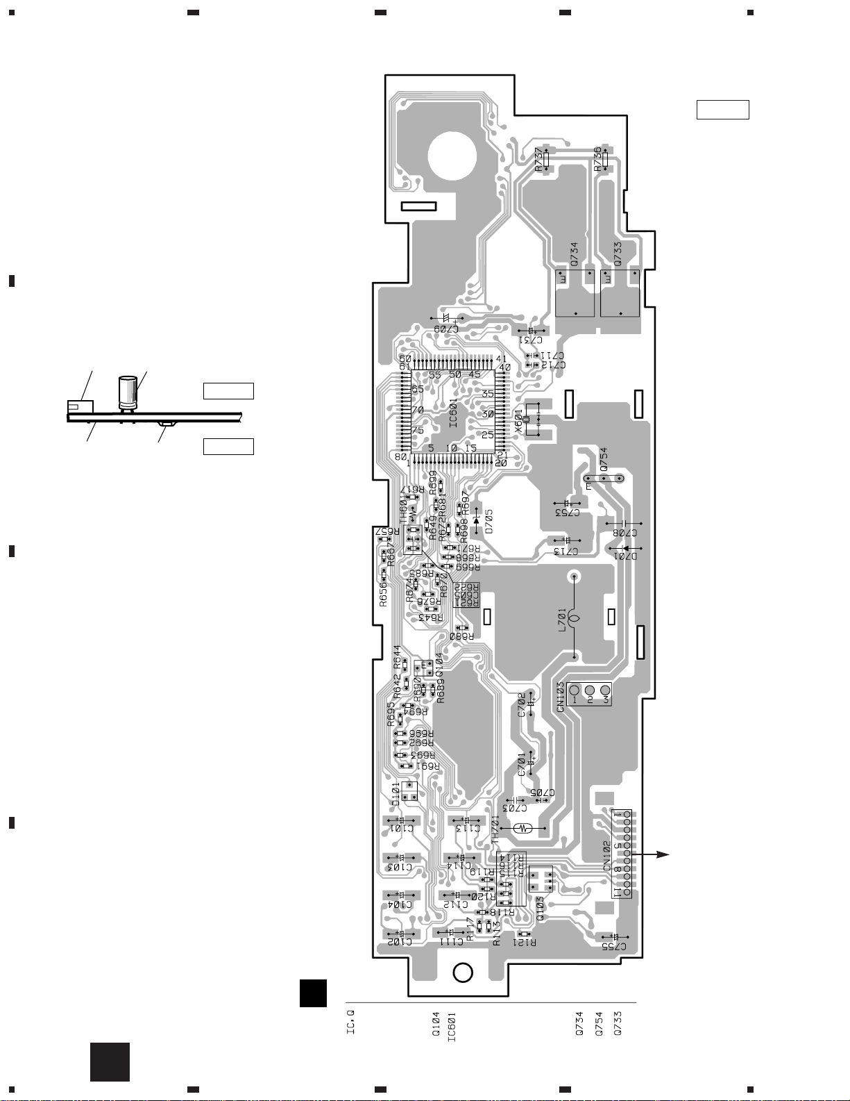
Unit Number : CWM6677
Unit Name : Extension Unit
MISCELLANEOUS
IC 101 IC NJM4558MD
IC 102 IC NJM4558MD
IC 103 IC TC74HC4066AF
IC 501 IC CA0008AM
IC 601 IC PD5540A
IC 701 IC PAJ002A
Q 101 Transistor DTC143TK
Q 102 Transistor DTC143TK
Q 103 Transistor FMC2A
Q 104 Transistor DTA124EU
Q 701 Transistor 2SA1162
Q 702 Transistor 2SB1189
Q 721 Transistor 2SC2712
Q 731 Transistor 2SC2712
Q 732 Transistor 2SA1162
Q 733 Transistor 2SD1760F5
Q 734 Transistor 2SD1760F5
Q 741 Transistor 2SK1485
Q 742 Transistor 2SK1485
Q 751 Transistor FMC2A
Q 753 Transistor FMW1
Q 754 Transistor 2SB1335A
D 101 Diode DAP202U
D 701 Diode ERA15-10Y1
D 702 Diode 1SS355
D 703 Diode 1SS355
D 704 Diode 1SS355
D 705 Diode MA1Z240
D 706 Diode 1SR154-400
D 721 Diode 1SS355
D 731 Diode HZU8R2(B3)
D 741 Diode DAN202U
D 751 Diode UDZS6R2(B)
L 701 Coil CTH1190
L 702 Inductor LCTB100K2125
TH 601 Thermistor CCX1032
TH 701 Switch CCX1047
X 601 Radiator 6.290MHz CSS1451
RESISTORS
R 101 RS1/16S332J
R 102 RS1/16S332J
R 103 RS1/16S333J
R 104 RS1/16S333J
R 105 RS1/16S103J
R 106 RS1/16S822J
R 107 RS1/16S822J
R 108 RS1/16S103J
R 109 RS1/16S153J
R 110 RS1/16S822J
R 111 RS1/16S822J
R 112 RS1/16S153J
R 113 RS1/16S104J
R 114 RS1/16S104J
R 115 RS1/16S104J
R 116 RS1/16S104J
R 117 RS1/16S221J
R 118 RS1/16S221J
R 119 RS1/16S221J
R 120 RS1/16S221J
R 121 RS1/16S103J
R 501 RS1/8S101J
R 502 RS1/8S101J
R 601 RS1/16S473J
R 602 RS1/16S473J
R 603 RS1/16S473J
R 604 RS1/16S102J
R 605 RS1/16S222J
R 606 RS1/16S222J
R 607 RS1/16S222J
R 608 RS1/16S222J
R 609 RS1/16S222J
R 610 RS1/16S222J
R 611 RS1/16S561J
R 612 RS1/16S561J
R 613 RS1/16S561J
R 614 RS1/16S561J
R 615 RS1/16S103J
R 616 RS1/16S103J
R 617 RS1/16S163J
R 618 RS1/16S222J
R 619 RS1/16S0R0J
R 620 RS1/16S473J
R 621 RS1/16S433J
R 622 RS1/16S103J
R 640 RS1/16S471J
R 641 RS1/16S471J
R 642 RS1/16S471J
R 643 RS1/16S471J
R 644 RS1/16S471J
R 649 RS1/16S222J
R 651 RS1/16S222J
R 652 RS1/16S471J
R 653 RS1/16S471J
R 654 RS1/16S471J
R 655 RS1/16S471J
R 656 RS1/16S471J
R 657 RS1/16S471J
R 658 RS1/16S471J
R 659 RS1/16S471J
R 660 RS1/16S471J
R 661 RS1/16S102J
R 662 RS1/16S102J
R 663 RS1/16S102J
R 664 RS1/16S102J
5. ELECTRICAL PARTS LIST
NOTE:
- Parts whose parts numbers are omitted are subject to being not supplied.
- The part numbers shown below indicate chip components.
Chip Resistor
RS1/_S___J,RS1/__S___J
Chip Capacitor (except for CQS.....)
CKS....., CCS....., CSZS.....
=====Circuit Symbol and No.===Part Name Part No.
--- ------ ------------------------------------------ -------------------------
=====Circuit Symbol and No.===Part Name Part No.
--- ------ ------------------------------------------ -------------------------
A
Page 45

43
CDX-MG6346ZH,MG6446ZH
R 665 RS1/16S102J
R 666 RS1/16S471J
R 667 RS1/16S471J
R 668 RS1/16S331J
R 669 RS1/16S331J
R 670 RS1/16S331J
R 671 RS1/16S331J
R 672 RS1/16S331J
R 673 RS1/16S471J
R 674 RS1/16S471J
R 675 RS1/16S471J
R 676 RS1/16S471J
R 677 RS1/16S222J
R 678 RS1/16S222J
R 679 RS1/16S222J
R 680 RS1/16S154J
R 681 RS1/16S222J
R 682 RS1/16S102J
R 683 RS1/16S912J
R 685 RS1/16S102J
R 689 RS1/16S103J
R 690 RS1/16S103J
R 691 RS1/16S273J
R 692 RS1/16S202J
R 693 RS1/16S512J
R 694 RS1/16S104J
R 695 RS1/16S104J
R 696 RS1/16S104J
R 697 RS1/16S222J
R 698 RS1/16S222J
R 699 RS1/16S222J
R 701 RS1/10S204J
R 702 RS1/16S104J
R 703 RS1/16S153J
R 704 RS1/16S473J
R 705 RS1/16S683J
R 706 RS1/16S473J
R 707 RS1/16S223J
R 708 RS1/8S101J
R 709 RS1/8S101J
R 711 RS1/16S103J
R 712 RS1/8S3R9J
R 713 RS1/16S102J
R 714 RS1/16S473J
R 715 RS1/16S473J
R 716 RS1/16S473J
R 717 RS1/16S473J
R 718 RS1/16S473J
R 719 RS1/8S101J
R 721 RS1/8S103J
R 722 RS1/16S473J
R 723 RS1/16S152J
R 731 RS1/10S681J
R 732 RS1/16S223J
R 733 RS1/16S103J
R 734 RS1/16S223J
R 735 RS1/16S223J
R 736 RS1/4S2R2J
R 737 RS1/4S2R2J
R 738 RS1/16S104J
R 741 RS1/16S223J
R 742 RS1/16S223J
R 743 RS1/16S103J
R 744 RS1/16S103J
R 751 RS1/16S101J
R 752 RS1/16S473J
R 753 RS1/10S223J
R 754 RS1/16S101J
R 755 RS1/4S221J
R 756 RS1/16S681J
R 757 RS1/16S511J
R 758 RS1/16S561J
R 759 RS1/16S103J
R 760 RS1/16S273J
CAPACITORS
C 101 CEV4R7M35
C 102 CEV4R7M35
C 103 CEV4R7M35
C 104 CEV4R7M35
C 105 CCSRCH101J50
C 106 CCSRCH101J50
C 107 CCSRCH101J50
C 108 CCSRCH101J50
C 109 CKSRYB473K16
C 110 CKSRYB473K16
C 111 CEV4R7M35
C 112 CEV4R7M35
C 113 CEV4R7M35
C 114 CEV4R7M35
C 501 CKSRYB102K50
C 502 CKSRYB102K50
C 503 CKSRYB104K16
C 601 CKSRYB104K16
C 603 CKSRYB103K50
C 605 CKSRYB103K50
C 651 CKSRYB103K50
C 701 CEAT471M16
C 702 CEAT471M16
C 703 CKSQYB104K25
C 704 CKSRYB223K25
C 705 CKSRYB103K50
C 706 CKSRYB103K50
C 707 CKSRYB103K50
C 708 CSZSC220M16
C 709 CCL1049
C 710 CKSRYB103K50
C 711 CKSRYB473K16
C 712 CKSRYB473K16
C 713 CEV100M16
C 721 CKSRYB103K50
C 731 CEV4R7M35
C 732 CKSRYB473K16
C 751 CKSRYB473K16
C 752 CKSRYB103K50
C 753 CEV220M16
C 754 CKSRYB473K16
C 755 CEV220M6R3
Unit Number : CWM6289
Unit Name : Keyboard Unit
MISCELLANEOUS
IC 901 IC BU2092FV
Q 903 Transistor 2SA1586
Q 904 Transistor DTC123JU
Q 905 Chip Transistor 2SC2712
D 901 Diode 1SS355
D 902 Diode 1SS355
D 903 Diode 1SS355
D 905 LED CL200PGCTU
D 906 LED CL150DCD(AB)
D 907 LED CL200PGCTU
D 908 LED CL150DCD(AB)
D 909 LED CL200PGCTU
D 910 LED CL150DCD(AB)
D 911 LED CL200PGCTU
D 912 LED CL150DCD(AB)
=====Circuit Symbol and No.===Part Name Part No.
--- ------ ------------------------------------------ -------------------------
=====Circuit Symbol and No.===Part Name Part No.
--- ------ ------------------------------------------ -------------------------
B
Page 46

44
CDX-MG6346ZH,MG6446ZH
D 913 LED CL200PGCTU
D 914 LED CL150DCD(AB)
D 915 LED CL200PGCTU
D 916 LED CL150DCD(AB)
D 917 Diode UDZ2R7(B)
D 918 Diode UDZ2R7(B)
S 901 Switch CSG1043
S 902 Switch CSG1043
S 903 Switch CSG1043
S 904 Switch CSG1043
S 905 Switch CSG1043
S 906 Switch CSG1043
S 907 Switch CSG1043
S 910 Spring Switch CSN1033
IL 901 Lamp 60mA 8V CEL1526
IL 902 Lamp 60mA 8V CEL1526
IL 903 Lamp 60mA 8V CEL1568
IL 904 Lamp 60mA 8V CEL1568
RESISTORS
R 901 RS1/10S561J
R 902 RS1/10S561J
R 903 RS1/10S561J
R 904 RS1/10S561J
R 910 RS1/8S511J
R 911 RS1/8S511J
R 912 RS1/8S511J
R 913 RS1/8S511J
R 914 RS1/8S511J
R 915 RS1/8S511J
R 916 RS1/8S511J
R 917 RS1/8S511J
R 918 RS1/8S511J
R 919 RS1/8S511J
R 920 RS1/8S511J
R 921 RS1/8S511J
R 931 RS1/8S510J
R 932 RS1/8S510J
R 934 RS1/10S223J
R 935 RS1/10S102J
R 936 RS1/10S103J
R 937 RS1/10S362J
R 938 RS1/10S472J
CAPACITORS
C 901 CKSQYB104K50
Unit Number : CWX2202
Unit Name : CD Core Unit(Servo Unit)
MISCELLANEOUS
IC 101 IC UPC2572GS
IC 201 IC UPD63702AGF
IC 301 IC BA5986FM
Q 101 Transistor 2SD1664
Q 102 Transistor UMD2N
D 301 Diode 1SR154-400
X 201 Ceramic Resonator 16.934MHz CSS1457
EF 201 Filter CCG1076
RESISTORS
R 101 RS1/8S100J
R 102 RS1/8S120J
R 104 RS1/16S822J
R 105 RS1/16S682J
R 106 RS1/16S183J
R 107 RS1/16S822J
R 108 RS1/16S333J
R 109 RS1/16S683J
R 110 RS1/16S134J
R 111 RS1/16S273J
R 112 RS1/16S222J
R 113 RS1/16S103J
R 114 RS1/16S103J
R 115 RS1/16S102J
R 116 RS1/16S163J
R 117 RS1/16S163J
R 120 RS1/16S101J
R 121 RS1/16S101J
R 125 RS1/16S0R0J
R 201 RS1/16S104J
R 202 RS1/16S103J
R 203 RS1/16S332J
R 204 RS1/16S752J
R 205 RS1/16S752J
R 206 RS1/16S101J
R 250 RS1/16S331J
R 251 RS1/16S331J
R 252 RS1/16S331J
R 253 RS1/16S331J
R 254 RS1/16S331J
R 255 RS1/16S471J
R 256 RS1/16S471J
R 259 RS1/16S221J
R 263 RS1/16S471J
R 269 RS1/16S0R0J
R 274 RS1/16S471J
R 277 RS1/16S471J
R 301 RS1/16S103J
R 302 RS1/16S153J
R 303 RS1/16S103J
R 304 RS1/16S273J
R 305 RS1/16S103J
R 306 RS1/16S752J
R 307 RS1/16S103J
R 308 RS1/16S103J
R 309 RS1/16S471J
R 311 RS1/16S471J
CAPACITORS
C 101 CEV101M6R3
C 102 CKSQYB104K16
C 103 CEV470M6R3
C 104 CKSQYB334K16
C 105 CCSRCH240J50
C 106 CKSRYB222K50
C 107 CEV4R7M35
C 108 CKSRYB273K25
C 109 CCSRCH101J50
C 110 CKSQYB104K16
C 111 CKSRYB332K50
C 112 CKSQYB473K16
C 113 CKSRYB103K25
C 114 CKSRYB391K50
C 115 CCSRCH121J50
C 116 CKSRYB682K50
C 117 CKSRYB333K16
C 118 CKSQYB334K16
C 119 CKSQYB334K16
C 120 CKSQYB334K16
C 121 CKSQYB334K16
C 122 CKSQYB104K16
C 123 CKSRYB472K50
C 124 CKSQYB104K16
C 125 CCSRCH5R0C50
C 126 CKSRYB153K25
C 127 CKSRYB102K50
C 201 CKSQYB334K16
C 202 CKSQYB104K16
C 203 CKSQYB104K16
=====Circuit Symbol and No.===Part Name Part No.
--- ------ ------------------------------------------ -------------------------
=====Circuit Symbol and No.===Part Name Part No.
--- ------ ------------------------------------------ -------------------------
C
Page 47

45
CDX-MG6346ZH,MG6446ZH
C 204 CKSRYB471K50
C 207 CKSQYB683K16
C 208 CKSRYB821K50
C 209 CKSRYB273K25
C 210 CKSQYB334K16
C 211 CKSQYB334K16
C 212 CKSQYB334K16
C 213 22µF/6.3V CCH1300
C 301 CEV101M10
C 302 CEV101M10
Unit Number : CWX2203
Unit Name : CD Core Unit(STS Unit)
MISCELLANEOUS
IC 501 IC CXD2511R
IC 502 IC
MSM514400DP-60TS
IC 601 IC AK4321VF
IC 701 IC BA05SFP
IC 801 IC LB1836M
IC 802 IC LB1836M
Q 801 Transistor DTA123JK
Q 802 Transistor UN2211
D 701 Diode 1SR154-400
D 702 Diode 1SR154-400
D 703 Diode 1SS355
D 704 Diode 1SS355
D 705 Diode 1SS355
D 706 Diode 1SS355
D 707 Diode 1SS355
D 708 Diode 1SS355
S 801 Spring Switch(LOAD) CSN1052
S 802 Spring Switch(DOOR) CSN1052
S 803 Spring Switch(MODE) CSN1052
EF 701 Filter CCG1051
EF 702 Filter CCG1051
RESISTORS
R 501 RS1/16S102J
R 502 RS1/16S202J
R 503 RS1/16S392J
R 504 RS1/16S822J
R 505 RS1/16S163J
R 506 RS1/16S512J
R 507 RS1/16S182J
R 508 RS1/16S222J
R 509 RS1/16S102J
R 510 RS1/16S102J
R 511 RS1/16S102J
R 512 RS1/16S102J
R 513 RS1/16S102J
R 514 RS1/16S471J
R 601 RS1/16S101J
R 602 RS1/16S101J
R 603 RS1/16S471J
R 604 RS1/16S471J
R 701 RS1/10S0R0J
R 702 RS1/10S100J
R 716 RS1/16S471J
R 717 RS1/16S471J
R 718 RS1/16S471J
R 801 RS1/10S102J
CAPACITORS
C 501 CKSQYB334K16
C 502 CKSQYB334K16
C 503 CKSQYB334K16
C 504 CCSRCH471J50
C 506 CCSRCH221J50
C 601 CKSQYB334K16
C 602 CCSRCH221J50
C 603 CKSQYB334K16
C 604 CKSQYB334K16
C 605 22µF/6.3V CCH1300
C 606 CKSQYB334K16
C 701 22µF/6.3V CCH1300
C 702 CEVL101M6R3
C 703 CKSQYB334K16
C 704 CKSQYB334K16
C 801 CKSQYB104K25
C 802 CKSQYB104K25
C 803 CEVL220M16
Unit Number :
Unit Name : Motor PCB(B)
M 4 Motor Unit(Carriage) CXB3178
M 5 Motor(Spindle) CXM1120
Unit Number :
Unit Name : Motor PCB(A)
Q 1 Photo-interrupter RPI-221
M 1 Motor Unit(Cam Gear) CXB3174
M 3 Motor Unit(ELV) CXB3175
Unit Number :
Unit Name : PCB Unit(D)
Q 851 Photo-transistor CPT230SCTD(CD)
Q 852 Photo-transistor CPT230SCTD(CD)
Unit Number :
Unit Name : PCB Unit(B)
S 886 Spring Switch(ELV Home) CSN1052
S 887 Spring Switch(Clamp) CSN1051
Unit Number :
Unit Name : PCB Unit(E)
R 856 RS1/8S911J
R 857 RS1/8S821J
Unit Number :
Unit Name : PCB Unit(C)
Q 881 Photo-transistor CPT230SCTD(CD)
D 883 Chip LED CL202IRXTU
S 885 Spring Switch(MAX) CSN1052
Unit Number :
Unit Name : Load Motor PCB
M 2 Motor Unit(Load) CXB3177
Unit Number :
Unit Name : PCB Unit(A)
D 891 Chip LED CL202IRXTU
D 892 Chip LED CL202IRXTU
Miscellaneous Parts List
Pickup Unit(Service)(P8) CXX1311
=====Circuit Symbol and No.===Part Name Part No.
--- ------ ------------------------------------------ -------------------------
=====Circuit Symbol and No.===Part Name Part No.
--- ------ ------------------------------------------ -------------------------
D
E
F
G
I
J
K
L
H
Page 48

46
CDX-MG6346ZH,MG6446ZH
6. ADJUSTMENT
CHECKING THE GRATING AFTER CHANGING THE PICKUP UNIT
• Note :
The grating angle of the PU unit cannot be adjusted after the PU unit is changed. The PU unit in the CD mecha-
nism module is adjusted on the production line to match the CD mechanism module and is thus the best adjusted
PU unit for the CD mechanism module. Changing the PU unit is thus best considered as a last resort. However, if
the PU unit must be changed, the grating should be checked using the procedure below.
• Purpose :
To check that the grating is within an acceptable range when the PU unit is changed.
• Symptoms of Mal-adjustment :
If the grating is off by a large amount symptoms such as being unable to close tracking, being unable to perform
track search operations, or taking a long time for track searching.
• Method :
• Measuring Equipment • Oscilloscope, Two L.P.F.
• Measuring Points • E, F, REFOUT
• Disc • ABEX TCD-784
• Mode • TEST MODE
• Checking Procedure
1. In test mode, load the disc and switch the 5V regulator on.
2. Using the TRK+ and TRK- buttons, move the PU unit to the innermost track.
3. Press key 3 to close focus, the display should read "91". Press key 2 to implement the tracking balance adjustment the display should now read "81". Press key 3 4 times. The display will change, returning to "81" on the
fourth press.
4. As shown in the diagram above, monitor the LPF outputs using the oscilloscope and check that the phase difference is within 75° . Refer to the photographs supplied to determine the phase angle.
5. If the phase difference is determined to be greater than 75° try changing the PU unit to see if there is any
improvement. If, after trying this a number of times, the grating angle does not become less than 75° then the
mechanism should be judged to be at fault.
• Note
Because of eccentricity in the disc and a slight misalignment of the clamping center the grating waveform may be
seen to "wobble" ( the phase difference changes as the disc rotates). The angle specified above indicates the average angle.
• Hint
Reloading the disc changes the clamp position and may decrease the "wobble".
100kΩ
390pF
100kΩ
390pF
E
REFOUT
F
Xch Ych
Oscilloscope
L.P.F.
L.P.F.
E
F
REFOUT
REFOUT
CD CORE UNIT(SERVO UNIT)
Page 49

47
CDX-MG6346ZH,MG6446ZH
Grating waveform
Ech → Xch 20mV/div, AC
Fch → Ych 20mV/div, AC
45°
0°
75°
60°
30°
90°
Page 50

48
CDX-MG6346ZH,MG6446ZH
7. GENERAL INFORMATION
7.1 DIAGNOSIS
7.1.1 TEST MODE
- CD Test Mode
1) Precautions on Adjustment
• The unit employs a single voltage (+5V) for the regulator, thus the reference potential of the signal is
RFOUT (approximately 2.5V) rather than GND.
Inadvertent contact of REFOUT and GND during
adjustment can result not only in disabling normal
potential measurement but also in exposing the pickup to strong impacts due to malfunctioning of the
servo. Therefore, you are requested to observe the
following precautions.
• Make sure that the negative probe of the measuring
instrument is not connected to RFOUT or GND.
Special care must be exercised so that the channel 1
negative probe may not be connected to the oscilloscope and the channel 2 negative probe to GND.
Since the frame of the measuring instrument is usually at the same potential as the negative probe, the
frame of the measuring instrument must be changed
to floating status.
When RFOUT is inadvertently connected to GND, you
must immediately turn off the regulator or power
supply.
• The regulator must be turned off before mounting or
dismounting filters or wiring materials.
• You should not start adjustment or measurement
immediately after the regulator is turned on. It is recommended to run the player for approximately one
minute so that it may stabilize.
• When the test mode is turned on, various protective
functions from the software become unavailable.
Thus, you must make sure that undesirable electric or
mechanical shocks are not be given to the system.
• This model employs a photo-transistor for detecting
discs at their loading or ejection. Thus, if its outer
case is removed during repair work and internal parts
are exposed to light of strong intensity, malfunctions
including the following can result:
∗ The eject button becomes inoperable during play.
Pressing the eject button does not eject a disc and
play is continued.
∗ Loading becomes unavailable.
If a malfunction is recognized, appropriate remedial
actions must be taken. Such actions include changing the light source position, changing the unit position and applying a cover to the photo-transistor.
• When you press the [EJECT] key to eject a disc, you
must not touch any other key until the ejection is
complete.
• If you press the [TRK+] or [TRK-] for the focus search
in the test mode, you must turn the power off immediately. (Otherwise, the lens will be forced to stick to
the top or bottom, potentially resulting in the burning
of the actuator.)
2) Description of the Test Mode
Adjustment of this unit is done in parallel with the CD
control unit (DEH-M7126ZH or a head unit conforming
to the GA-NET BUS specifications), thus key operations for adjustments are done from the unit. Taking
the example of the DEH-M7126ZH, the following
describes how to turn on the test mode and operate
the keys. The keys referred to in the following are
those used on the DEH-M7126ZH.
• Turning on the Test Mode
Press the [4] and [6] keys simultaneously to turn on
the ACC and the backup.
• Ending the Test Mode
When ACC or Back up is off, the test mode is canceled.
• Operation of TR JUMPs (except 100TR) continues
after your finger has left the key. CRG MOVE and
100TR JUMP are forced to the tracking close mode as
soon as the key is released.
• Turning the power on or off resets the JUMP MODE
to the Single TR.
Page 51

49
CDX-MG6346ZH,MG6446ZH
[ASEL]
Power Off
[3]
Focus Close/S-curve/
F, EQ Measurement
[6]
Focus Mode Select
[1]
Tracking Servo
Close
[ASEL]
Power ON
(T.OFFSET adjustment required)
[3]
Power ON
(T.OFFSET adjustment not required)
[1]
Mechanism Test Mode
Initial State
[CD]or[DISC]
Source CD
MIN
TRK
[ASEL]
Power Off
[1]
Tracking Close
(AGC, Applicable Servo)
[6]
Tracking Close
(No AGC, Applicable Servo)
[3]
Auto Adjustment Display
/Rough Servo
[2]
Tracking Balance
Adjustment
[Key]
Contents
Display
[4]+[6]+Reset
Test Mode In
[3]
AGC
[6]
CRG/TR Jump Count
Select
[TRK+]
CRG+/TR Jump+
[TRK-]
CRG–/TR Jump–
[4]
SPINDLE
Uniform/
Double Switching
[ASEL]
Power Off
[1]
AGC/F.BIAS
Display Switching
or
[TRK+]
CRG+
[TRK-]
CRG-
[TRK+]
CRG+
[TRK-]
CRG-
[ASEL]
Power Off
[2]
Trackig Open
[2]
Trackig Open
*1
*6
*5
*3
*2
*2
*4
*1) Switching must take place in the following sequence.
S.Curve Check
Focus EQ Measurement.Focus Close
*2)
→→ → → →
9X(8X):91(81)
4 TR
92(82)
10 TR
93(83)
32 TR
94(84)
100 TR
95(85)
CRG Move
96(86)
*4)
→→→
F.AGC Gain F.AGC Gain F. BIAS Setting
(AGC Gain = (Current value/Initial value) x 20)
→→→
→→
Single TR /4TR / 10TR / 32TR / 100TR
Single TR
*3) Switching must take place in the following sequence.
It applies to the CRG Move and 100TR Jump alone.
Min/Sec (or Track No.)
*5) Switching must take place in the following sequence.
F.Cancel Display
*6) Switching must take place in the following sequence.
T.Offset Display T.Bal Display
Rough Servo.
(F.Bias value, F.Cancel value, T.Offset value, T.Bal value
= (Upper 8 bits of the setting (7F[H] to 80[H] + 128)/4
= 63[D] to 32[D] to 00[D]).
•
•
•
Operation of TR JUMPs other than 100TR is continued after your finger has left the key.
CRG Move and 100TR Jump are forced to the Tracking Close Mode when the key is released.
Powering on or off resets the Jump Mode to the Single TR (91).
When ACC or Back up is off, the test mode is canceled.
Note:
Note:
Note:
The GA-NET BUS head unit(made by Pioneer) must be employed for controlling the test mode.
Sound is unavailable even after the tracking has been closed
(this trouble results when the IC for the STS is not controlled in the test mode).
When you pressed the [TRK+] or [TRK-] key during the Focus Search, you must turn the power off immediately
(otherwise, the lens can stick resulting in actuator damages).
[Key]
[ASEL]
[TRK+]
[TRK-]
[1]
[2]
[3]
[4]
[5]
[6]
Operation
Power ON/OFF
CRG+/TR Jump+
(Toward outer perimeter)
Tracking Close/AGC gain,
F.Bias adjustment value display switching
Auto Tracking Balance adjustment/
Tracking Open
Focus Close, S.Curve, F.EQ measurement/
Rough Servo/AGC
Focus Open
/SpindleUniform/Double Switching
Jump Off
Focus Mode select/Tracking Close/
CRG,TR Jump Switching
CRG-/TR Jump(Toward inner perimeter)
or
or
or or
or
or
Note: To exchange CD's, insert or eject a CD, use numerical buttons 1 to 6 on the CD changer.
(During the test mode, even when no disc is stored on a tray. If so, first press the EJECT button once.)
SEC
MIN
TRK
00 00
SEC
00
MIN
TRK
99 99
SEC
99
MIN
TRK
SEC
MIN
TRK
91 91
SEC
91
MIN
TRK
0X 0X
SEC
0X
MIN
TRK
00 00
SEC
00
MIN
TRK
99 99
SEC
99
MIN
TRK
SEC
MIN
TRK
XX XX
SEC
XX
MIN
TRK
XX XX
SEC
XX
MIN
TRK
?? ??
SEC
??
MIN
TRK
SEC
MIN
TRK
?? ??
SEC
??
MIN
TRK
XX XX
SEC
XX
MIN
TRK
XX XX
SEC
XX
MIN
TRK
72 0*
SEC
**
MIN
TRK
00 00
SEC
00
MIN
TRK
99 99
SEC
99
MIN
TRK
00 00
SEC
00
MIN
TRK
99 99
SEC
99
MIN
TRK
8X 8X
SEC
8X
MIN
TRK
9X 9X
SEC
9X
MIN
TRK
8X 8X
SEC
8X
MIN
TRK
9X 9X
SEC
9X
MIN
TRK
8X 8X
SEC
8X
MIN
TRK
XX XX
SEC
XX
MIN
TRK
8X 8X
SEC
8X
MIN
TRK
9X 9X
SEC
9X
MIN
TRK
XX
SEC
XX
MIN
TRK
8X 8X
SEC
8X
MIN
TRK
9X 9X
SEC
9X
MIN
TRK
XX XX
SEC
XX
MIN
TRK
SEC
MIN
TRK
00 00
SEC
00
MIN
TRK
99 99
SEC
99
(
)
MIN
TRK
00 00
SEC
00
MIN
TRK
99 99
SEC
99
(
)
MIN
TRK
00 00
SEC
00
MIN
TRK
99 99
SEC
99
(
)
- CD Player Flowchart
Page 52

50
CDX-MG6346ZH,MG6446ZH
[ASEL]
Mecha Test Out
CD Test In
[1]
CAM MOTOR
select
[2]
ELV MOTOR
select
[3]
LOAD MOTOR
select
[1]
Mechanism Test In
Initial State
[ASEL]
CD Test Mode
[CD]or[DISC]
Source CD
[Key]
Contents
Display
[4]+[6]+Reset
Test Mode In
[4]
CAM+LOAD MOTOR
select
[TRK+]
MOTOR FWD drive
- Operating Procedures:
1)
2)
3)
Turn on the CD Test Mode, then select the
CD-CHANGER for the SOURCE.
Select the motor to be driven
using the [1] to [3] ,[6] keys.
Press the [TRK+] or [TRK-] in this state to drive
the selected motor.
[Key]
[ASEL]
[TRK+]
[TRK-]
[1]
[2]
[3]
[4]
Operation
Mechanism Test is initialized.
Valid only when the motor selected (using the
[1] to [3] ,[6] keys) is driven in FWD direction.
CAM MOTOR is selected.
[3]
CD Test Mode
[TRK-]
MOTOR REV drive
Valid only when the motor selected (using the
[1] to [3] ,[6] keys) is driven in REV direction.
ELV MOTOR is selected.
LOAD MOTOR is selected.
CAM + LOAD MOTOR is selected.
<Screen Display during Mecha Test Mode>
TRK : 72
MIN : Upper (10th order):
Type of motors selected
Lower (order of 1): State of DISC
sensing phototransistor and switch
1* : CAM motor
2* : ELV motor
3* : LOAD motor
4* : CAM+LOAD motor
PH1 PH2
MAXSW
Display
L
H
L
H
L
H
L
H
L
L
H
H
L
L
H
H
L
L
L
L
H
H
H
H
*0
*1
*2
*3
*4
*5
*6
*7
L:H:Phototransistor is OPEN and switch is ON.
Phototransistor is CLOSE and switch is OFF.
SEC : 1 When ELV motor is selected, ELV position is displayed
01: ELV at home position (1st disc).
10: ELV at a position other than home (2nd to 6th).
11: ELV moving to a specified position. * Note 1
00: Reserved (for an error)
2 When CAM.LOAD motor is selected:
Indicates CAMSW (CAM gear) status.
EJECT
SW1 (DOORSW)
SW2 (LOADSW)
SW3 (MODESW)
SW4 (CLAMPSW)
Display
10
30
31
21 20
222333 32
REV
FWD
Note 2
- Precautions
*
Note 1:
Note 2:
While the CD mechanism is moving to exchange CDs, eject or insert a CD, never
perform key operations for motor selection or drive operation.
When driving the CAM MOTOR in 31 → 30 → 10 (in REV direction),
the elevation position must be at the EJECT/LOAD position (the top position).
When the elevation is situated at the Note 1 position, move of any motor
other than the REV is disabled.
Before performing the elevation, make sure that the CAM SW (switch) is
set to a position between 22 and 20.
As a rule, driving of the ELV MOTOR must be started immediately after
the CAMSW indication has changed from 22 to 20.
clamp
MIN
TRK
SEC
MIN
TRK
72 0*
SEC
**
MIN
TRK
SEC
MIN
TRK
72 1*
SEC
**
MIN
TRK
72 2*
SEC
**
MIN
TRK
00 00
SEC
00
MIN
TRK
99 99
SEC
99
MIN
TRK
72 3*
SEC
**
MIN
TRK
72 4*
SEC
**
MIN
TRK
72 **
SEC
**
MIN
TRK
72 **
SEC
**
MIN
TRK
72 X*
SEC
**
(
)
*
- CD Changer Mechanism Flowchart
Page 53

51
CDX-MG6346ZH,MG6446ZH
- Operating Procedures for Ejecting a Clamped Disc
1
2
3
4
5
6
Select CAM MOTOR using [1], then press the REV direction while the disc is being clamped (CAMSW state is 32).
The CAMSW status indication sequentially changes through 32→33→23→22.
When the disc to be ejected is not identical with the disc being clamped, select the [2] ELV MOTOR in the vicinity of where
the display changes from 22 to 20, then match the elevation to the disc to be ejected according to the following procedures:
After selecting ELV MOTOR, lower the elevation until the ELV position display becomes 01 (1st disc) using the REV direction.
Drive the elevation up until the display is changed to 10. This is the elevation where the second disk is situated.
The next display of 10 tells you the elevation of the 3rd disc. Repeating this operation allows you to establish an elevation
matching each disc. (When the elevation is driven from the 1st through 6th disc, the status display changes as
01→11→10→11→10→11→10→11→10→11→10.)
(When the disc to be ejected coincides with the disc being clamped, the above operations are not necessary.)
Select the [1] CAM MOTOR and then, using the REV direction, drive it until the display changes from 20 (or 22) to 21 and 31.
Select the [2] ELV MOTOR, then drive the tray of the disc to be ejected up to the EJECT/LOAD position (using the FWD direction).
Select the [4] CAM+LOAD MOTOR, then drive it in the REV direction until the display changes from 31 to 30 and 10.
The door will open immediately before the display changes to 10 and part of the disc will be pushed out.
When 10 is displayed, select the [3] LOAD MOTOR, then drive it in REV direction until the disc is completely ejected.
Page 54

7.1.2 DISASSEMBLY
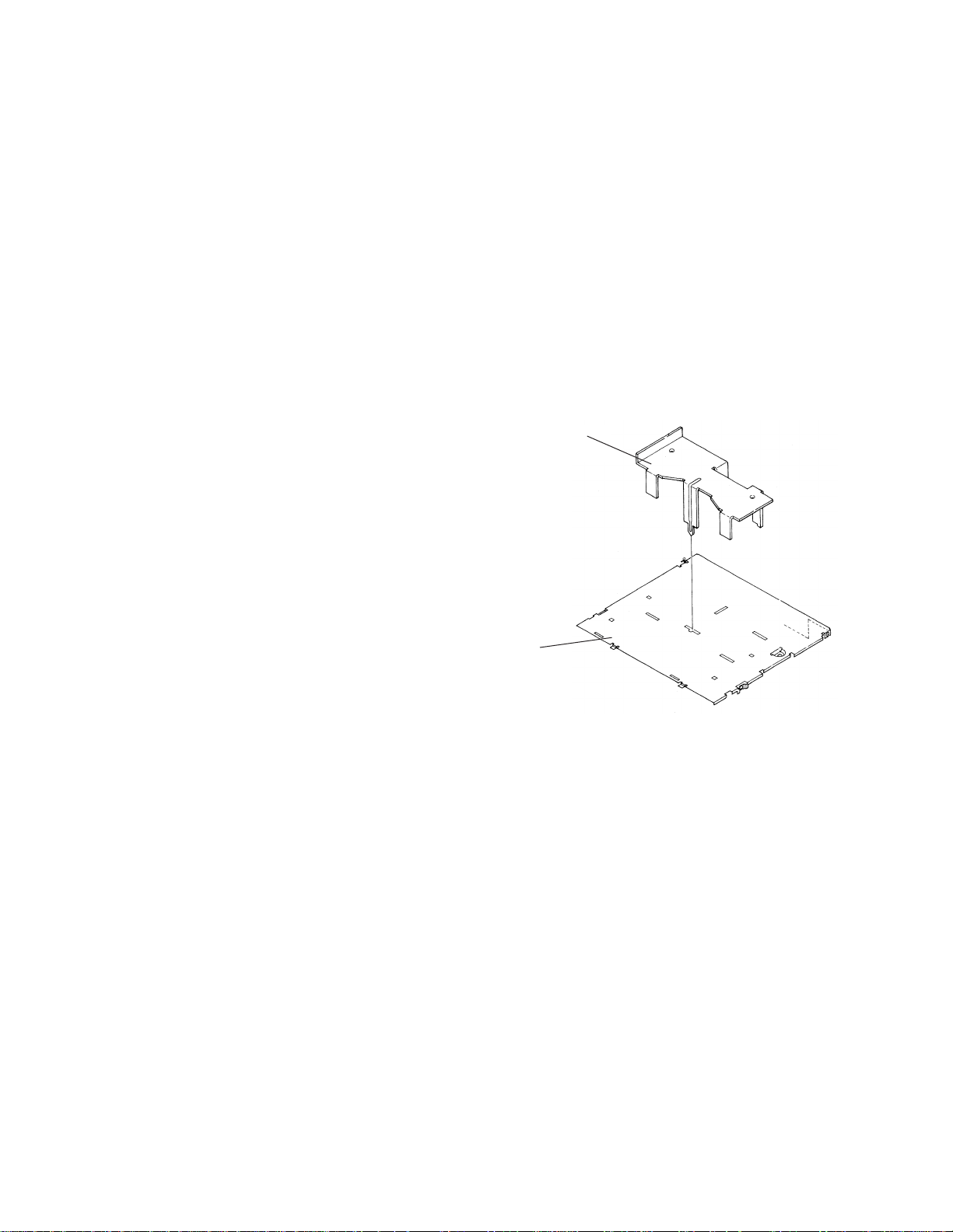
- Removing the Extension Unit (Fig. 1)
1. Remove the three screws B, then remove the side
frame and holder.
2. Remove the screw C, screw D and PCB from the
connector.
3. Straighten the three currently bent claws, then
remove the extension unit.
- Removing the CD Mechanism Module (Fig. 2)
1. Remove the three screws A, then remove the
front frame.
2. Remove the three screws B and two screws C,
then remove the damper and holder.
3. Remove the two spring As, spring B and spring
C from the hook, then remove the CD mechanism module.
- Removing the Keyboard Unit (Fig. 3)
1. Remove the screws A and four screws B, then
remove the keyboard unit.
2. Remove the four screws C, then remove the
guide.
– Precautions on Assembly –
Apply spring C (black) to the front
side hook.
Remaining springs A and B are to be
hung on the center hook.
Fig. 1
Fig. 2
Fig. 3
- Removing the Grille Assy (Fig. 1)
1. Remove the two screws A and the connector,
then remove the grille assy.
- Removing the upper case (not shown)
1. Remove the five screws, then remove the upper
case.
52
CDX-MG6346ZH,MG6446ZH
Page 55

53
CDX-MG6346ZH,MG6446ZH
- How to remove the Tray Assy
1. Apply about 6V current to the Cam gear motor until
all holes match at the position (A) (elevation OK position).
2. Hook the three springs B temporarily as shown in Fig.
5. While pushing the Tray holder lock arms (right and
left) in the direction (C), remove the Tray holder.
3. Lift up the Tray assy to remove it.
* Be careful not to remove the Tray hooks from the Tray
assy.
- How to remove the Carriage Mech Assy
1. Insert a short pin into the flexible PCB of the Pickup
unit.
2. While opening the resin hooks, remove the cover
from the Servo unit.
3. Disconnect the flexible PCBs from the connectors
CN101 and CN301.
4. Remove the Tray holder and the Tray assy. (See
above)
5. Rotate the Cam gear motor until the positions of all
holes (E) match, then stop the motor.
(The Carriage Mech assy will stop as shown in the
Fig.7.)
* When the positions of all holes match, they will be
completely covered by the Carriage mech assy.
* To rotate the Cam Gear motor, see "How to remove
the Tray assy".
6. Unhook the spring A.
7. Remove the flexible holder B (while opening the
hooks).
8. Remove the flexible PCB (C) from the motor. (The
flexible PCB (C) has been stuck on the motor with
double-sided adhesive tape.)
9. Loosen the fixing screw and remove the flexible
holder.
ELV motor
Cam gear motor
Approximately DC 6V
Tray holder
Tray holder lock arm
Tray holder
lock arm
Tray
hooks
Tray Assy
Cover
CN101
CN301
Match the hole positions
Flexible
holder
Fig.4
Fig. 5
Fig. 6
Short pin
Tray
hooks
Page 56

54
CDX-MG6346ZH,MG6446ZH
- How to remove the Pickup unit
1. Remove the pulling spring, torsion spring and Eshaped ring. Then remove the Clamper arm.
* The spring (A) will be removed with the Clamper
arm.
10. Remove the screw, pressure spring and collar. Lift
up the Carriage mechanism assy to remove it.
* Screw tightening torque: 2.6kgfcm
2. Slide the Clamp UP lever (B) to remove it.
3. Loosen the 2 screws. Remove the feed-screw cover
by sliding it.
4. Remove the feed-screw pressure spring (D).
5. Loosen the 2 screws. Remove the feed-screw holder
(E).
6. Remove the belt.
7. Remove the Pickup unit together with the feed screw.
* Be careful not to lose the shaft holders at the both
ends of the feed screw.
* Be careful not to damage the 2 flexible PCBs(for the
Pickup and motor) when separating them. The flexible PCBs have been stuck each other with doublesided adhesive tape.
Carriage mechanism Assy
Screw
Collar
Pressure spring
Clamper arm
E-shaped ring
Pulling spring
Torsion spring
White
Black
Pickup
unit
Feed screw
Belt
Carriage
motor
Fig. 7
Fig. 8
Fig. 9
Page 57

55
CDX-MG6346ZH,MG6446ZH
8. Loosen the 2 screws. Remove the plate spring and
the rack.
9. Pull out the feed screw from the Pickup unit.
Rack
Plate spring
Feed screw
Pickup
unit
Grease (White: KD-1)
Grease (Yellow:
PG-641)
Fig. 10
Grease (Yellow:
PG-641)
Page 58

56
CDX-MG6346ZH,MG6446ZH
7.1.3 CONNECTOR FUNCTION DESCRIPTION
14
13
12
11
10
9
8
7
6
5
4
3
2
1
1 Lch+
2 Rch+
3 AGND
4 GND
5 SWDACC
6 B.UP
7 Lch8 Rch9NC
10 BUS GND
11 BUS12 BUS+
13 ILL
14 NC
Page 59

57
CDX-MG6346ZH,MG6446ZH
7.2 IC
- Pin Functions (PD5540A)
Pin No. Pin Name I/O Function and Operation
1 VDIN I VD power supply sensor input
2 DOORSW I Door open position sense input
3 NHIN I NH-BUS dada input
4 NHOUT O NH-BUS dada output
5 CLAMPSW I Disk clamp sense input
6 ELHOME I Elevation sense input
7 XSCK O LSI clock output
8 XSO O LSI data output
9 XSI I LSI data input
10 xstb O LSI strobe output
11 xrst O LSI reset output
12 XA0 O LSI data discernment control signal output
13 VDCONT O VD power supply control output
14 EJECTKEY I Eject key input
15 asens I ACC power sense input
16 NHPOW O NH-BUS dada output
17 LOADSW I Loading sense input
18 ELVSW I Elevation OK input
19–21 TEST1-3 Not used
22 bsens I Back up power sense input
23 sbsy I Signal indicating head of subcode block input
24 isens I Illumination sense input
25 reset I Reset input
26 POWER O +5V power supply control output
27 CONT O Servo driver power supply control output
28 XIN I Crystal oscillating element connection pin
29 XOUT O Crystal oscillating element connection pin
30 VSS GND
31–33 KST1-3 O Key strobe output
34,35 kd!,@ I Key data input
36,37 ILL1,2 O Illumination output
38 ASCON O Analog switch control output
39 testin I Test program mode input
40 DCLOSE I Door close sense input
41 WDSL O Data comparison designation output
42 XWIH I DRAM data white inhibit input
43 XEMP I DRAM data read inhibit input
44 CHDT I Data comparison mode monitor input
45,46 CHM0,1 O Data comparison mode output
47-49 NC Not used
50 XWRE O DRAM data white enable output L:enable
51 XRDE O DRAM data read enable output L:enable
52 XQOK O SUB-Q OK output L:SUBQ OK
53 EMPH O DAC EMPH output
54 SCONT O Double speed select output
55 LOAD O LED power supply control output
56 cdmute O Mute output
57,58 LO2,1 O Load motor control output
59,60 ELV2,1 O ELV motor control output
61,62 CG2,1 O CAM motor control output
63 MIRR I Mirror detector input
64 LOCK I Spindle lock detector input
65 FOK I FOK signal input
66 EXSCK O Shift clock output
67 EXMODE O Latch clock output
68 EXSO O Serial data output
Page 60

58
CDX-MG6346ZH,MG6446ZH
Pin No. Pin Name I/O Function and Operation
69 EXCE O Chip enable output
70 ILPOW O Illumination power supply control output
71 VCC Power supply terminal
72 VREF I A/D converter reference voltage input
73 AVSS I A/D converter GND
74 ADRMON I DRAM memory remaining monitor input
75 EREF I DRAM A/D converter reference voltage input
76-78 PH1-3 I Disc photo sense input
79 ELVSNS I ELV position sense input
80 TEMP I Temperature detector input
80
1
20
21 40
41
60
61
*PD5540A
IC's marked by* are MOS type.
Be careful in handling them because they are very
liable to be damaged by electrostatic induction.
20
19
18
17
VDD
oe
Q11
Q10
16
15
14
13
Q9
Q8
Q7
NC
12
11
NC
Q6
1
2
3
4
VSS
DATA
CLOCK
LCK
5
6
7
8
Q1
Q2
Q3
Q4
9
10
Q5
Q0
Output buffer (Open drain)
12bit storage-register
12bit shift-register
Control circuit
BU2092FV
Page 61

59
CDX-MG6346ZH,MG6446ZH
MSM514400DP-60TS
20
19
18
16
VSS
DQ4
DQ3
oe
17
cas
15
14
13
11
A8
A7
A6
A4
12
A5
1
2
3
5
4
6
7
8
10
9
DQ1
DQ2
we
A9
ras
A0
A1
A2
VCC
A3
Timing
Generator
Column
Address
Buffers
Timing
Generator
Column
Decoders
Write
Clock
Generator
Internal
Address
Counter
Refresh
Control
Clock
Sense
Amplifiers
I/O
Selector
Output
Buffers
Input
Buffers
Row
Address
Buffers
Row
Decoders
Word
Drivers
Memory
Cells
On Chip
Vbb Generater
10
10
10
10
4
4
4
4
4
4
4
28
27
26
25
PreVcc
OPIN4(+)
OPIN4(-)
OPOUT4
24
23
22
OPIN3(+)
OPIN3(-)
OPOUT3
21
20
19
18
GND
STBY
PowVcc
VO3(-)
17
16
15
VO3(+)
VO4(-)
VO4(+)
1
2
3
4
BIAS IN
OPIN1(+)
OPIN1(-)
OPOUT1
5
6
7
OPIN2(+)
OPIN2(-)
OPOUT2
8
9
10
11
GND
MUTE
PowVcc
VO2(-)
12
13
14
VO2(+)
VO1(-)
VO1(+)
Stand-by
Mute
Level shift
Level shift
Level shift
Level shift
BA5986FM
Page 62

60
CDX-MG6346ZH,MG6446ZH
1
2
3
4
CHDT
AM19
AM18
AM17
5
6
7
8
AM15
TST0
VSS
SPSL
9
10
XRST
AM16
11
12
13
14
TST1
DTSL
CHM0
CHM1
15
16
XWRE
WDSL
17
18
19
20
XRDE
XQOK
XSOE
SDTO
21
22
23
24
SCK
XLT
VDD
DATA
25
26
BCK
SDTI
27
28
29
30
LRCK
WDCK
WDCI
LRCI
31
32
BCKI
DATI
48
47
46
45
XOE
XCAS
D3
D2
44
43
42
41
D0
MCSL
C176
VSS
40
39
XTLI
D1
38
37
36
35
XTLO
OSCE
NC
MCK
34
33
RFCK
XROI
64
63
62
61
XEMP
XWIH
NC
A4
60
59
58
57
A6
A7
A8
VDD
56
55
A3
A5
54
53
52
51
A2
A1
A0
A9
50
49
XWE
XRAS
Timing
controller
CPU
interface
VWA
register
CK
generator
WA
generator
RA
generator
Remain area
calcurator
S/P
P/S
Status
controller
Data
comparator
RAM
interface
Selector
CXD2511R
Page 63

61
CDX-MG6346ZH,MG6446ZH
8. OPERATIONS AND SPECIFICATIONS
8.1 OPERATIONS
LOADING THE CD (1 of 2)
CD Loading Slot
Disc status LED
6 DISC IN-DASH CD CHANGER
Disc Number Buttons
Flashes green
Flashes green and orange
1
EXPLANATION OF THE HAND MARKS
The CD Changer operates with the same controls used for the audio system. For operation, refer to the audio system section of the Owner’s Manual for your radio.
Press momentarily. Press and hold for at least 3 seconds.
3SEC
Press one of the buttons (1–6) to
select the desired disc number for
the CD you want to load.
• LED flashes green.
After a few seconds the CD loading
slot door opens, and the LED flashes green and orange. (Green t
Orange t Green t Orange)
• If you do not load a CD within about 15
seconds, the door will close. Pressing the
same disc number button again or pressing the eject button will cause the door to
close.
LOADING THE CD (con’t)
Disc status LED
6 DISC IN-DASH CD CHANGER
CD Loading Slot
2
Notes: • Repeat steps ¡ and ™ to load CDs in other disc numbers.
• The unit may go into CD eject mode when it detects improper CD loading. Wait 2
seconds before inserting the CD for loading.
Insert the CD with the label side up.
• When loading is complete, LED will stop
flashing and remain lit.
Note: This unit is not designed to handle
8 cm CD’s.
Do not attempt to load it alone or with
adapter. It may cause the unit to
malfunction.
You can load a CD under a selected disc number. The system will
automatically playback when the CD is loaded.
Page 64

62
CDX-MG6346ZH,MG6446ZH
SELECTING A CD
Disc status LED
6 DISC IN-DASH CD CHANGER
Disc Number Buttons
Flashes orange
1
Press one of the buttons (1–6) to
select a desired CD for play.
• Green LED indicates CDs are stored and
orange LED indicates currently selected
CD.
• While CDs are being changed, the LED
flashes orange until CD changing has
been completed, then it lights orange.
• You can also select a desired CD by
using preset buttons or upward button on
the radio.
EJECTING THE CD (1 of 2)
Disc status LED
6 DISC IN-DASH CD CHANGER
Disc Number Buttons
Eject Button
Lights green
≠
Flashes orange
≠
Lights orange
1
2
Then press eject button to eject the
CD.
• The LED flashes green and the CD is
ejected.
Press one of the buttons (1–6) to
select the disc number for the CD
you want to eject.
EJECTING THE CD (con’t)
Disc status LED
Eject Button
Disc Number Buttons
6 DISC IN-DASH CD CHANGER
Note: If you do not remove the ejected CD
from the CD loading slot within about
15 seconds, it is automatically
reloaded. If you press the eject button,
or press the ejected CD’s disc number
button (the Disc status LED that’s
flashing green), the CD is immediately
reloaded.
Note: If you leave the ejected CD in the CD
loading slot, and press the disc
number button for a CD that’s loaded
(the Disc status LED is lit green), the
ejected CD is reloaded and the CD
loaded in the disc number you
selected is ejected instead. This
function is convenient when the
ejected CD is different from the one
you want to eject.
Notes: • Pull the CD out. The LED flashes green and orange, and this product switches to the
CD loading standby mode.
• You can eject CDs even if the ignition is switched OFF. In this case, you cannot perform step ¡ to select a CD. When you press the eject button, the currently selected
CD is ejected.
Also, when you pull a CD out, the door immediately closes. (This unit does not switch
to the CD loading standby mode.)
Page 65

63
CDX-MG6346ZH,MG6446ZH
8.2 SPECIFICATIONS
General
Power source ................. 13.2 V DC (10.8 – 15.2 V allowable)
Grounding system ........................................... Negative type
Standby current .................................................. 2 mA or less
Rated current consumption ............................. 600 mA max.
Maximum current consumption .......................... 1.5 A max.
Dimensions (chassis size) .... 180 (W) x 50 (H) x 165 (D) mm
Weight ............................................................................ 1.6 kg
CD player
System ....................................... Compact disc audio system
Usable discs ...................................................... Compact disc
Signal format ......................... Sampling frequency: 44.1 kHz
....................................Number of quantization bits: 16;linear
Frequency characteristics ................................. 5 – 20,000 Hz
Signal-to-noise ratio ............... 93 dB (1kHz) (IHF-A network)
Dynamic range ................................................... 92 dB (1kHz)
Number of channels ................................................ 2 (stereo)
ILLUMINATION
6 DISC IN-DASH CD CHANGER
Eject Button
3SEC
1
The illumination color changes each
time you press and hold the eject
button for 3 seconds or longer.
This product is equipped with two illumination colors, white and orange.
You can select the desired illumination color.
Page 66

PIONEER ELECTRONIC CORPORATION 4-1, Meguro 1-Chome, Meguro-ku, Tokyo 153-8654, Japan
PIONEER ELECTRONICS SERVICE INC. P.O.Box 1760, Long Beach, CA 90801-1760 U.S.A.
PIONEER ELECTRONIC [EUROPE] N.V. Haven 1087 Keetberglaan 1, 9120 Melsele, Belgium
PIONEER ELECTRONICS ASIACENTRE PTE.LTD. 253 Alexandra Road, #04-01, Singapore 159936
C PIONEER ELECTRONIC CORPORATION 1999
K-ZZS. FEB. 1999 Printed in Japan
ORDER NO.
CRT2376
CD MECHANISM MODULE
CX-890
CONTENTS
1. MAIN PARTS LOCATIONS........................................2
2. CIRCUIT DESCRIPTIONS ..........................................3
3. MECHANISM OPERATIONS...................................16
4. DISASSEMBLY........................................................21
NOTE:
- This Service Manual outlines operations of the CD mechanism module used in the models listed blow.
- For repair, use this Service Manual and the Service Manual of the model used in the system.
Model Service manual CD mechanism module CD mechanism unit
CDX-PD6/UC CRT2372 CXK4701 CXB2700
Page 67

2
CX-890
1. MAIN PARTS LOCATIONS
Frame
Stage front side
Carriage motor (M4)
ELV motor (M2)
Cam gear motor (M1)
Photo interrupter (ELV)
Loading motor (M3)
Servo unit
Disc insertion detectors
Disc insertion detectors
Clamp switch
(S887)
ELV HOME switch
(S886)
Disc ejection detectors
Detection switch
(S885)
STS unit
Spindle
motor (M5)
Insertion completion
switch
Mode switch
(S803)
Door switch
(S802)
Load switch
(S801)
Do not hold the upper frame of the disc insertion slot or
the front side of the stage in the CD mechanism module when
servicing to prevent them from being deformed.
- CD Player Service Precautions
1. For pickup unit(CXX1311) handling, please refer
to"Disassembly"(Page 21).
During replacement, handling precautions shall be
taken to prevent an electrostatic discharge(protection
by a short pin).
2. During disassembly, be sure to turn the power off
since an internal IC might be destroyed when a connector is plugged or unplugged.
Page 68

3
CX-890
2. CIRCUIT DESCRIPTIONS
2.1 Preamplifier (UPC2572GS: IC101)
The preamplifier processes pickup output signals to
generate signals to be sent to the servo, demodulator,
and controller. The preamplifier with built-in photodetector converts signals from the pickup into intermediate voltage in the pickup. Then, addition is made in the
RF amplifier (IC101) to obtain RF, FE, TE, and TE zero
cross signals. The system consists of the UPC2572GS
and other components explained below. The system
uses a single power source (+5 V). Therefore, the reference voltage of IC101 and the reference voltage of the
power unit and servo circuit are REFOUT (+2.5 V). REFO
UT is obtained from REFOUT of servo LSI (IC201:
UPD63702GF) via a buffer, and is output from Pin 19 of
IC101. This REFOUT is used as reference for all measurements.
Note:Do NOT short-circuit REFOUT and GND during
measurement.
1
2
3
4
5
6
7
8
9
10
11
12
13
14
15
16
17
18
19
38
37
36
35
34
33
32
31
30
29
28
27
26
25
24
23
22
21
20
X12
RF
envelope
AGC
Detection
X3
Phase detection
3T detection
Bottom
DC shift
Peak
Control
DC shift
Bottom
Peak
120kΩ
DEFECT circuit
FE
BAL
FE
BAL
Vcc
Mirror circuit
FE
BAL
APC
X2
Vcc
FE-BAL
TE-BAL
ASY
EFM-OUT
C.DEF
DEFECT
RFOK
MIRR
3T-OUT
C.FE
FE-OUT
FE-
GND
TE-
TE-OUT1
TE-OUT2
DET-IN
DET-OUT
VREF-INVREF-OUT
LDON
LD
PD
E
F
D
B
C
A
Vcc
C2.3T
C1.3T
RF-
RF-OUT
RF-IN
C AGC
AGC-OUT
EFM-IN
HPF
TE
BAL
EFM comparator
Control
Fig. 1 Block Diagram of UPC2572GS
1) Automatic Power Control (APC) circuit
Laser diode has negative temperature characteristics
with great optical output when the diode is driven with
constant current. Therefore, current must be controlled
by a monitor diode to ensure constant output. Thus
functions the APC circuit. LD current can be obtained by
measuring the voltage between LD1 and GND. The current value is approximately 35 mA.
Vcc (5V)
Vr
LD MD
UPC2572GS
16
PD
17
LD
15
Q101
2SD1664
C124
0.1µF
C101
(100µF/6.3V)
R101
10Ω
LD1
R102
12Ω
5V
CONT
Q102 UMD2N
18
5V
5V
1kΩ
150kΩ
16kΩ
R112
2.2kΩ
C104
0.33µF
5
1kΩ
2.5V
Pickup unit
Fig. 2 APC Circuit
Voltage between LD1 and GND(mv)
LD current(mA) =
10 Ω + 12 Ω
Page 69

4
CX-890
2) RF amplifier and RF AGC amplifier
Photodetector outputs (A+C) and (B+D) are added,
amplified and equalized in IC101, and output to the RFI
terminal as RF signal. (Eye pattern can be checked at
this terminal.)
Low-frequency components of voltage RFI is:
RFI = ((A + C) + (B + D)) x 3.22
where R111 is offset resistor to keep RFI signal within
the output range of the preamplifier. RFI signal is goes
under AC coupling, and is input to Pin 4 (RFIN terminal).
IC101 contains an RF AGC circuit. RFO output from Pin
2 is maintained to a constant level (1.2 ±0.2 Vp-p). The
RFO signal is used in the EFM, DFCT, and MIRR circuits.
3) EFM circuit
The EFM circuit converts RF signal into digital signals of
"0" and "1". RFO signal after AC coupling is input to Pin
1, and supplied to the EFM circuit.
Asymmetry caused during manufacturing of discs cannot be eliminated solely by AC coupling. Therefore, the
system controls the reference voltage ASY of the EFM
comparator by using the fact that probability to generate "0" and "1" is 50% in EFM signal. This reference voltage ASY is generated by output from the EFM comparator through L.P.F. EFM signal is output from Pin 35.
As signal level, amplification is 2.5 Vp-p around
REFOUT.
4) DFCT (defect) circuit
DFCT signal detects mirror defect in discs, and is output
from Pin 33. The system outputs "H" when a mirror
defect is detected.
If disc is soiled, the system determines it as lack of mirror. Therefore, the system inputs the DFCT signal output to the HOLD terminal of servo LSI. Focus and tracking servo drives change to Hold status only when DFCT
output is in "H" so that performance of the system upon
detection of defect can be improved.
5) RFOK circuit
The RFOK circuit outputs signal to show the timing of
focus closing servo, as well as the status of focus closing during playback. The signal is output from Pin 32.
The system inputs the RFOK signal output to the RFOK
terminal of servo LSI. The servo LSI issues Focus Close
command. The system outputs signal in "H" during
focus closing and playback.
CN101
13
6
DETECT
13
11
10
10kΩ
20kΩ
9.3kΩ
RFI
+5V
R111
27kΩ
Vcc
×12
ASY
12
20kΩ
(RF AGC)
AGC
RF
ENVELOPE
HPF
VDC
RFOK
20kΩ
33
36
35
34
PEAK
DEFECT
EFM
UPC2572GS
A+C
10kΩ
B+D
9.3kΩ
20kΩ
10kΩ
10kΩ
R105
6.8kΩ
C125 5pF
C105
24pF
R125
0R0
R104
8.2kΩ
RFIN
C107
4.7µF/35V
C122
0.1µF
C106
RFO
REFOUT (+2.5V)
DEFECT
BOTTOM
R107 8.2kΩ
R106 18kΩ
C111 3300pF
C110
C112 0.047µF
6 54 3 21
32
0.1µF
2200pF
HOLD
Fig. 3 RF AMP, RF AGC, EFM, DFCT, RFOK Circuit
Page 70

5
CX-890
6) Focus-error amplifier
The system outputs photodetector output (A+C) and
(B+D) as FE signal (A+C)-(B+D) from Pin 28 via the difference amplifier, then via the error amplifier.
Low-frequency components of voltage FEY is:
An S curve equivalent to approximately 1.6 Vp-p is
obtained at FE output (Pin 28) by using REFO as reference. The cut-off frequency of the amplifier of the last
layer is 12.4 kHz.
7) Tracking-error amplifier
Outputs E and F from the photodetector are output as
TE signal (E-F) from Pin 24 via the difference amplifier,
then via the error amplifier.
Low-frequency components of voltage TEY is:
TE waveforms equivalent to approximately 1.5 Vp-p are
obtained at TE output (Pin 24) by using REFO as reference. The cut-off frequency of the amplifier of the last
layer is 19.5 kHz.
8) Tracking zero-cross amplifier
Tracking zero-cross signal (TEC signal) is generated by
amplifying TE waveforms (voltage at Pin 24) by a factor
of four. The signal is used for detecting the zero-cross
point of tracking error in the servo LSI UPD63702AGF.
The purposes of detecting the zero-cross point are as
follows:
(1)To be used for counting tracks for carriage move and
track jump.
(2)To be used for detecting the direction of lens move-
ment when tracking is closed. (To be used in the
tracking brake circuit mentioned later.)
The frequency range of TEC signal is from 500 Hz to
19.5 kHz.
Voltage TEC = TE level x 4
In other words, the TEC signal level is calculated as 6
Vp-p. This level exceeds the D range of the operation
amplifier, resulting in the signal to clip. However,
there shall be no problem, since the servo LSI uses
only zero-cross point.
65
9.3kΩ
9.3kΩ
20kΩ
10kΩ
10kΩ
6
13
13
12
10kΩ
10kΩ
20kΩ
FE VCA
38
REFOUT
C114
390pF
FE
R108
33kΩ
28
27
17.2kΩ
50pF
gm=1/68.8kΩ
90kΩ
10
11
CN101
A+C
B+D
F.BAL
REFOUT (+2.5V)
gm CONDUCTANCE
UPC2572GS
Fig. 4 Focus-error amplifier
Fig. 5 Tracking-error amplifier,
Tracking zero-cross amplifier
CN101
R117
16kΩ
R116
16kΩ
14
15
9
11
31kΩ
31kΩ
50pF
63kΩ
C123
4.7nF
R114
10kΩ
R113
10kΩ
TBAL
C115
120pF
R109
68kΩ
R115
1kΩ
C126
15nF
TE
4R
R
F
E
23
TEC
C116
6.8nF
TE VCA
gm=1/17kΩ
63kΩ
37
24
5pF
TOFST
R110
130kΩ
50pF
25
REFOUT (+2.5V)
gm CONDUCTANCE
UPC2572GS
63kΩ 68kΩ
TEY=(E-F) X X
(31kΩ+16kΩ) 17kΩ
: (TE level of pickup unit x 5.36)
20kΩ 90kΩ R108
FEY=(A+C)-(B+D)X X X
10kΩ 68.8kΩ 17.2kΩ
: (FE level of pickup unit x 5.02)
Page 71

6
CX-890
9) MIRR (mirror) circuit
MIRR signal shows ON and OFF track information. The
signal is output from Pin 31.
The status of MIRR signal is as follows:
Laser beam ON track: MIRR = "L"
Laser beam OFF track: MIRR = "H"
The signal is used in the brake circuit mentioned later.
10) 3T OUT circuit
The system detects flickering of RF signal when disturbance is input to the focus servo loop, and outputs the
difference of phase between FE signal and RF-level
fluctuation signal from Pin 30. The resulting signal is
obtained through L.P.F. with a fc of 40 Hz. This signal is
used for automatic adjustment of FE bias.
MIRR
COMP
DC
shift
PeakAGC
Bottom
RFO
Detection
A
1.5V
UPC2572GS
(Peak) – (Bottom)
4
31
RFIN
B
Z
C
RFO
PEAK HOLD
BOTTOM HOLD
MIRROR
1
A
0
False MIRR caused by dirt
True MIRR
OFF TRACK
Dirt, etc.
B
C
Z
Ø
3T-OUT
FE signal
RFIN
UPC2572GS
C113
10nF
FEY
3T detection
C117
0.033µF
120kΩ
L.P.F
Phase detection
8
+
H.P.F
10kΩ
10kΩ
1kΩ
C2.3T
C109
100pF
C1.3T
C108
0.027µF
8
7
30
29
4
AGC
Differential
rectification
3T LEVEL ENVELOPE
DETECTOR
Phase
comparison
Fig.6 MIRR Circuit
Fig. 7 MIRR Circuit
Fig. 8 3T OUT Circuit
Page 72

7
CX-890
2.2 Servo (UPD63702AGF: IC201)
The servo consists of mainly two parts. The first part is
the servo processing unit to equalize error signals and
control track jump, carriage move, in focus, etc. The
second part is the signal processing unit to perform
data decoding, error correction, and interpolation.
The system converts FE and TE signals from analog to
digital in IC201, then outputs drive signals of the focus,
tracking, and carriage systems via the servo block. The
EFM signal input from the preamplifier is decoded by
the signal processing unit, and eventually output as
audio signal after conversion into analog from digital
signals via the DA converter (IC201 contains audio
DAC). Then, the system generates error signal for the
spindle servo in the decoding process, sends the signal
to the spindle servo to generate drive signal for spindle.
After that, drive signals for focus, tracking, carriage,
and spindle are amplified in IC301 and BA5986FM, and
supplied to respective actuators and motors.
1) Focus servo system
The main equalizer of focus servo is located in the
UPD63702AGF. Fig. 9 shows block diagram of the focus
servo.
For the focus servo system, the lens must be positioned within the focusing range in order to perform
focus closing. To achieve this, the system moves the
lens upward/downward by focus-search voltage of triangular waveform to detect the focusing point. During
searching, the system kicks the SPDL motor to maintain rotation speed to set speed.
The servo LSI monitors FE and RFOK signals so that
focus closing is performed automatically at an appropriate point.
Focus closing is performed when the following four
conditions are satisfied:
(1)When the lens moves nearer to the disc.
(2)RFOK = "H"
(3)FZD signal (in IC) is latched to "H"
(4)FE = 0 (REFOUT as reference)
FOCUS
ERROR
D/A
FD
FIN
DRIVER
FOP
FOM
IC301
BA5986FM
LENS
IC 201 UPD63702AGF
76
64
2
4
3
14
13
FOCUS SEARCH
TRIANGULAR WAVE
GENERATOR
DAC
DIGITAL
EQUALIZER
CONTROL
A/D
R301
10kΩ
R302
15kΩ
Fig. 9 Focus servo block diagram
Page 73

8
CX-890
When the conditions mentioned above are satisfied and
focus is closed, the XSO terminal changes from "H" to
"L". Then, the microcomputer starts monitoring RFOK
signal through L.P.F after 40 ms.
If the system judges RFOK signal as "L", the microcomputer takes actions, including protection.
Fig. 10 shows operations related to focus closing. (The
illustration shows when the system cannot perform
focus closing.) S curve, search voltage, and actual lens
behavior can be checked by pressing the Focus Close
button when "01" is shown in Focus Mode Select in Test
mode.
REFOUT
FD
LENS POSITION
RELATIVE TO DISC
NEAR
FAR
"JUST FOCUSED"
SIN
REFOUT
Expanding around "Just Focused Point"
REFOUT
RFI
FOK
FEX
FZD
THRESHOLD
LEVEL
FZD
(INTERNAL SIGNAL)
Focus closing would normally take place at these points
XSO
(IN THE EVENT
FOCUS IS
CLOSED)
LEVEL
Fig. 10 Sequence of Focus Closing
Page 74

9
CX-890
2) Tracking servo system
The main equalizer of tracking servo is located in the
UPD63702AGF. Fig. 11 shows block diagram of the
tracking servo.
a) Track jump
Track jump is automatically performed by the auto
sequence function in LSI when the LSI accepts command. The system has six types of jump (1, 4, 10, 32,
32x2, and 32x3) for truck jump during searching. In Test
mode, the system can select and check these jump
types and CRG move by selecting a mode. The microcomputer sets half of the total number of track jumps
(two tracks if the total number of tracks are four), and
counts the set number of tracks by using TEC signal.
The system outputs brake pulse for a specified time (set
by the microcomputer) from the point of time when the
set number is counted, and stops the lens. Thus, tracking is closed, and the system can continue normal playback.
To improve servo withdrawal during track jump, the
system sets the brake circuit to ON for 60 ms after
brake pulse so that gain of the tracking servo can be
increased.
FF/REV in normal mode is made by continuously performing single jump approximately ten times faster
than in normal playback.
TRACKING
ERROR
D/A
TD
TIN
DRIVER
TOP
TOM
IC301
BA5986FM
LENS
IC 201 UPD63702AGF
77
11
12
JUMP
PARAMETERS
DAC
DIGITAL
EQUALIZER
CONTROL
A/D
5
7
6
R303
10kΩ
R304
27kΩ
63
t1
t2
GAIN NORMAL
TIN
KICK
BRAKE
TEC
T. BRAKE
EQUALIZER
T. SERVO
CLOSED
OPEN
NORMAL
GAIN UP
OFF
ON
t1
TIN
TEC
(10 TRACK)
EQUALIZER
T. BRAKE
SERVO
CIN
2.8mS (4.10 TRACK JUMP)
5.8mS (32 TRACK JUMP)
GAIN UP
NORMAL
ON
OFF
OPEN
CLOSED
t2
60mS
t
Fig. 11 Tracking servo block diagram
Fig. 12 Single track jump
Fig. 13 Multi track jump
Page 75

10
CX-890
b) Brake circuit
Servo withdrawal will deteriorate during setting and
track jump. Thus, the system uses the brake circuit to
provide stable withdrawal to servo loop.
The brake circuit detects the direction of lens movement, and outputs only drive signal in the opposite
direction from the lens movement. Thus, the system
delays the speed of the lens movement to stabilize
withdrawal of the tracking servo.
The system judges sliding direction of track from TEC
and MIRR signals, as well as the relationship of their
phase.
TEC
TZC
(TEC "SQUARED UP" )
(INTERNAL SIGNAL )
MIRR
MIRR LATCHED AT
TZC EDGES
=
SWITCHING PULSE
EQUALIZER OUTPUT
(SWITCHED)
DRIVE DIRECTION
Note: In the illustration, the phase of equalizer output is shown as the same as with that of TEC.
FORWARD
LENS MOVING FORWARDS
(INNER TRACK TO OUTER)
LENS MOVING BACKWARDS
Time
REVERSE
Fig. 14 Tracking Brake Circuit
Page 76

11
CX-890
3) Carriage servo system
Output from low-frequency components (lens position
information) of the tracking equalizer is input to the carriage equalizer by the carriage servo. After obtaining a
certain gain, the system outputs drive signal from the
servo LSI. The signal is then applied to the carriage
motor via the driver IC. More specifically, the pickup
unit as a whole must be moved forward when lens offset during playback reaches a specified level. Therefore,
gain of equalizer is set so that voltage higher than the
activation voltage of the carriage motor is output. As
actual operation, a certain threshold level is set for
equalizer output in the servo LSI, and drive voltage is
output from the servo LSI only when the equalizer output level exceeds that level. Thus, power consumption
is reduced. Depending on eccentricity, etc. of disc, the
equalizer output voltage may cross the threshold level
several times before the pickup unit as a whole starts
operation. At this time, waveforms of drive voltage
from LSI are output as pulse.
D/A
SD
DRIVER
COP
COM
IC301
BA5986FM
CARRIAGE
MOTOR
IC201 UPD63702AGF
62
27
26
25
16
15
KICK, BRAKE
REGISTERS
DAC
DIGITAL
EQUALIZER
CONTROL
FROM
TRACK
EQUALIZER
M
R305
10kΩ
R306
7.5kΩ
CIN
DRIVE ON/OFF THRESHOLD
CARRIAGE MOVED AT THESE POINTS
TRACKING DRIVE
(LOW FREQUENCY)
LENS POSITION
CRG DRIVE
(INSIDE UPD63702AGF)
CRG MOTOR VOLTAGE
Fig. 15 Carriage Servo Circuit
Fig. 16 Carriage Signal Waveforms
Page 77

12
CX-890
4) Spindle servo system
The spindle servo has the following modes:
(1)Kick mode:To be used for accelerating disc rotation
during setting.
(2)Offset mode:
a)To be used after completion of kick until comple
tion of spindle lock during setting.
b)If focus is out of range during playback, this mode
is used until focus is recovered. In both cases,
Offset mode is used for maintaining disc rotation
to the speed close to specified rotation.
(3)Adaptive Servo mode: CLV servo mode during nor-
mal operation. The system samples every WFCK in
16 cycles whether frame synchronous signal matches output from the internal frame counter in EFM
demodulation block, and generates signal that
shows matching/unmatching status. If signal showing unmatching status continues for 8 times, the system deems it as asynchronous status. Except this
case, the system judges as synchronous. In Adaptive
Servo mode, the system automatically selects withdrawal servo for asynchronous status, and steadystate servo for synchronous status.
(4)Brake mode: Mode to stop the spindle motor.
The microcomputer outputs brake voltage from the
servo LSI. Waveforms of EFM are monitored inside
the LSI. If the longest pattern of EFM exceeds specified intervals (if the rotation speed adequately
slowed down), flag is activated in the LSI, and the
microcomputer turns brake voltage to OFF. If no flag
is activated after a specified time, the microcomputer changes from Brake to Stop mode. This status
continues for a specified time. If the system changes
to Stop mode during ejection, disc is ejected after
the specified time mentioned above.
(5)Stop mode: To be used when the power is turned to
ON, and during ejection. In Stop mode, the end-toend voltage of the spindle motor is 0 V.
(6)Rough Servo mode: To be used when returning car-
riage (carriage move during long search, etc.). The
system calculates linear speed from waveforms of
EFM, and inputs either "H" or "L" level to the spindle
equalizer. This mode is also used for confirmation of
grating in Test mode.
MDXMDY
DRIVER
IC301
BA5986FM
IC 201 UPD63702AGF
61
24
22
23
DSP
BLOCK
DAC
DIGITAL
EQUALIZER
EFM
69
SPEED AND
PHASE ERROR SIGNAL
SIN
R308
10k
Ω
R307
10k
Ω
R206
100Ω
Fig. 17 Spindle servo block diagram
Page 78

13
CX-890
2.3 Automatic Adjustment Function
With this system, all circuit adjustments are automatically performed by using the preamplifier (UPC2572GS)
and servo LSI (UPD63702AGF). All adjustments are
automatically performed whenever disc is inserted or
CD mode is selected by the Source key. Details of automatic adjustments are as follows:
1) Setting of FZD cancellation
This setting ensures focus closing. The system reads
the FE offset level when the power is turned to ON,
then writes the inverse voltage of offset value of that
level to CRAM inside IC to cancel offset. Thus, the
threshold level of FZD can be set to a constant value
(+150 mV). As a result, "Latching FZD signal to H",
which is one of the conditions required for focus closing in IC, is ensured.
2) TE offset automatic adjustment
Adjusts TE amplifier offset of the preamplifier to 0 V
when the power is turned to ON.
Adjustment is made as follows:
(1)The microcomputer reads TE offset in LD OFF status
via the servo LSI (TE1).
(2)The microcomputer calculates the voltage to be cor-
rected using the TE1 value, and outputs from Pin 65
(pin name: TOFST) of the servo LSI. More specifically, calculation is made as follows:
TOFST2 = TOFST1 + TE1 x R110 / R109
3) Tracking balance (T.BAL) automatic adjustment
To make the sensitivity of Ech of TE output equal to that
of Fch. In fact, adjustment is made so that the upper
and lower portions of TE waveforms are symmetric to
REFOUT.
Adjustment is made in the following steps:
(1)After focus close, the system kicks the lens in the
radial direction to ensure TE waveforms to be generated.
(2)The microcomputer reads the peak bottom of TE
waveforms via the servo LSI.
(3)The microcomputer calculates the amount of offset,
then calculates the voltage to be corrected based on
that offset. The system outputs the result from Pin 66
(pin name: TBAL) of the servo LSI.
(4)The voltage output from the servo LSI is input to Pin
37 of the preamplifier (IC101: UPC2572GS). Pin 37 is
a control-voltage terminal of the TEVCA amplifier.
According to voltage input, the system changes gain
of Ech and Fch in the preamplifier, and adjusts the
tracking balance to make the upper and lower portions of TE waveforms symmetric to REFOUT.
4) FE bias automatic adjustment
Maximizes the RFI level by optimizing focus point during playback. Adjustment is made by using 3T level
waveforms of RF waveforms and the phase difference
generated by input of disturbance of focus error. Since
adjustment is made by inputting disturbance to focus
loop, the system uses the same timing as with auto
gain control (mentioned later~) for adjustment.
Adjustment is made in the following steps:
(1)Disturbance is input to focus loop by the command
from the microcomputer (inside the servo LSI).
(2)The system detects flickering of 3T components of
RF signal in the preamplifier.
(3)The system checks the phase difference between 3T
components mentioned above and FE signal caused
by input of disturbance to detect the direction of
focus deviation. The result is output as DC voltage
from Pin 30 (3TOUT) of the preamplifier.
(4)The 3TOUT voltage is input to Pin 75 (A/D port) of the
servo LSI. The microcomputer reads this 3TOUT voltage via the servo LSI.
(5)The microcomputer calculates the amount of correc-
tion required. The results are transferred to offset of
focus loop in the servo LSI.
As with auto gain control, the system repeats the
same adjustment process several times to improve
adjustment precision.
Fig. 18 Outline of Automatic Adjustment
AGC
circuit
FE signal
TE signal
Constant RF level
IC101
UPC2572GS
Corrected
voltage
output
Detection
of deviation
Items of
automatic
ADJ
FZD
TE.O
T.BAL
FE.B
F and T.G
D/A
FZD FE.B Gain
A/D
IC201
UPD63702AGF
Transfer
of amount
of correction
Reading
amount of
deviation
System
microcomputer
Calculation
of amount
of correction
RF signal
TE.O, T.BAL
Page 79

5) Auto gain control (AGC)
AGC adjustment is already used in the CD modules of
the previous generation. This function automatically
adjusts servo loop gain of focus and tracking.
Adjustment is made in the following steps:
(1)Disturbance is input to servo loop.
(2)The system extracts error signals (FE and TE) upon
input of disturbance via the B.P.F. and obtains signals
of G1 and G2.
(3)The microcomputer reads G1 and G2 signals via the
servo LSI.
(4)The microcomputer calculates required amount of
correction to adjust loop gain in the servo LSI.
The system repeats the same adjustment process
several times to improve adjustment precision.
6) Initial adjustment value
For all automatic adjustments, the system uses the previous adjustment value as initial values, except when
the power of the microcomputer has been turned to
OFF (backup is turned to OFF). If backup has been
turned to OFF, the system uses initial set value to perform automatic adjustment.
7) Display of coefficients of adjustment results
Results of automatic adjustments can be displayed in
Test mode for confirmation. Display of coefficients in
each automatic adjustment is as follows:
(1)FZD cancel, TE.OFST cancel, T.BAL, and FE bias
Reference = 32 (32: No adjustment was required)
Display is made in units of approximately 40 mV.
Example: Coefficient of FZD cancel = 35
35 - 32 = 3 3 x 40 mV = 120 mV
Corrected amount is approximately +120 mV.
Thus, FE offset before adjustment is -120 mV.
(2)Adjustment of F and T gain
Reference: Focus = 13, tracking = 20
The amount of reduced gain in comparison with the
reference is known by looking at the coefficient dis
played.
Example: AGC coefficient = 40
Amount of reduced gain = 20 log (20/40) = -6dB
2.4 Power Supply and Mechanism
Control
The power supply VM (7.5V) is produced from the
power supply VD (9.0V) supplied from the extension
P.C. board, and used as the power supply for the loading motor driver, elevation motor driver, cam gear
motor driver, and 5V Reg IC. As for the drive voltage
for the disc detection LEDs and the power supply for
the CD driver ICs, the power supply VD (9.0V) is used.
The system IC controls the ON/OFF operations of the
CD driver and laser diodes,the 5V power supply, and
the drive voltage PVD for detection LEDs with "CONT",
"POWER", and "LOAD" signals respectively.
14
CX-890
Page 80

15
CX-890
2.5 STS(Sure Track System) Circuit
By pooling the musical data read in from a compact disc into the memory, even if the pickup should go off track for
some reason, the Sure Track System enables prevention of sound interruption during recovery (approximately 3 seconds) by continuing to output data from the memory.
Operation Principle
The STS circuit is controlled by the vibration free memory controller (CXD2511R). Data read in at double speed
from a compact disc is input via the digital signal processing circuit into CXD2511R.
CXD2511R stores this DA data in DRAM (MSM5114400
DP-60TS), and reads and outputs the data at normal
speed in synchronization with the internally generated
FS system clock. In order to write the DA data at double
speed and to read out at normal speed, the DRAM
becomes full, but when it reaches capacity it will tentatively stop reading data. (The CD is in the pause mode
during this time.) When an available area is created by
data read-out from the DRAM, data writing will start
again. (The available area of the DRAM can be monitored by ADRMON. By repeating this process, the
DRAM is always used effectively, and approximately
2.67 seconds worth data can be stored. Even if the pickup should go off track due to vibrations for example, if
recovered within 2.67 seconds while using the memorized data, sound interruption can be prevented.
Fig. 19
Fig. 20
Page 81

16
CX-890
3. MECHANISM OPERATIONS
3.1 Disc Insertion
a)The Cam gear rotates to the elevation OK position
(See "How to remove the Tray Assy" on page 21). The
Stage Mech Assy moves upwards or downwards to
reach the height of the selected tray by using the elevation mechanism.
b)The Cam gear rotates counterclockwise until the
LOAD switch is turned off. The Beak arms of the
Stage Mech ASSY driven by the Cam gear's movement lift the selected tray.
c)The Stage Mech Assy with the tray lifted moves to the
top position using the elevation mechanism.
* Disc insertion/ejection is performed at the top position
(the 6th stage) irrespectively of tray position.
d)The Cam gear rotates counterclockwise to move the
LOAD arms as shown in Fig.21.
e)The LOAD arms push the disc loaded on the tray and
open the tray hooks.
f)When a disc is inserted, the disc interrupts the infrared
LED light from the photo transistors, and the Rubber
roller starts rotating.
* The photo transistors are connected in serial. When
the light is interrupted from either photo-transistor,
the start of disc insertion will be detected.
g)The disc is drawn in. Then the disc pushes the inser-
tion completion switch via the arm.
h)The LOAD arms move forward to be released from
the disc. At the same time, the tray hooks close to
hold the disc on the tray.
Cam gear
Load switch
Beak arm
Stage mech Assy
Load arm
Load arm
Insertion completion switch
Disc
Tray hook
Load arm
Photo transistors
Fig. 21: Elevation OK position
Fig. 22
Page 82

17
CX-890
3.3 Elevation Detection
a)The elevation detection (slit count) is performed by
the photo interrupter.
b)After the elevation HOME switch is turned ON, the
photo interrupter counts the slits of the elevation
levers.
* The bottom position (the 1st stage) is detected when
the elevation HOME switch is turned on (not detected
by the photo interrupter).
3.2 Elevation
a)The Cam gear rotates to the elevation OK position.
b)The ELV motor rotates to slide the elevation lever via
the gears.
c)The 2 elevation levers (left and right) can synchronize
their sliding via the joint arm.
d)The shafts of the Stage Mech Assy engage with the
stair-like grooves in the elevation levers and the verti-
cal holes in the Main chassis via the rollers.
e) When the elevation levers slide, the Stage Mech Assy
moves up and down.
ELV motor
Photo interrupter
Elevation lever
Elevation
HOME switch
joint arm
Elevation lever
Fig. 23
Page 83

18
CX-890
3.4 Disc Clamp
a)The Stage Mech Assy moves up and down to reach
the height of the selected tray, using the elevation
mechanism.
b)The Cam gear rotates clockwise, the Carriage drive
arm rotates, and then the Carriage Mech Assy moves
toward the disc via the Carriage drive shaft.
c)The Cam gear continues rotating clockwise and the
Carriage drive shaft moves the Clamp UP lever. Then
the Clamp arm touching the Clamp UP roller moves
down to clamp the disc.
d)The Cam gear stops when the Clamp switch is turned
ON.
Clamp UP lever
Clamp arm
Clamp UP roller
Carriage Mech Assy
Carriage drive shaft
Carriage drive arm
Clamp switch
Fig. 24
3.5 Disc Sense (Initializing)
a)The disc sense operation is to detect if or not a disc is
loaded on the trays 1 to 6.
b)While a disc is inserted using the robber rollers, the
disc pushes the insertion completion switch via the
arm to sense that a disc is loaded.
3.6 Disc Ejection
a)The same operations as the steps a) to e) on "3.1 Disc
insertion" are performed.
b)The rubber roller(s) rotate(s) in the direction for disc
ejection.
c)When the infrared LED light, which has been inter-
rupted by the disc, passes toward the photo transistors, the rubber rollers stops.
Page 84

19
CX-890
3.7 Mechanism Lock
a)Mechanism lock operation is to push the mechanism
downward and toward the disc slot in order to keep
the mechanism at the correct position during disc
insertion/ejection, and to leave the appropriate gap
above the mechanism.
b)The Cam gear rotates to move the Mech lock lever
toward the rear of the Mechanism. The lever pushes
the inside surface of the product. It causes the mechanism to move forward.
c)With the movement of the Mech lock lever, the Mech
lock lever (right) moves in a slanting direction as indi-
cated by the arrow in Fig. 25 to push the mechanism
forward and downward.
d)The Mech lock lever (left) is driven by the movement
of the Mech lock lever via the Mech lock junction
lever to push the Mechanism downward.
e)The mechanism lock is released only in the disc
clamp mode.
Mech lock lever
Mech lock lever (left)
Mech lock junction
lever
Mech lock lever (right)
Fig. 25
Door switch
Door lever
Cam gear
Door open lever
Fig. 26
3.8 Door Open
a)The Door open lever pushes the door on the product
grille to open it.
b)The Cam gear rotates to move the door arm. Then,
the door arm moves the door lever.
c)The door lever moves the door open lever via the
buffer spring.
d)When the door switch is turned ON, the Cam gear
motor stops rotating.
Page 85

20
CX-890
3.9 Stage Mechanism Lock
a)To prevent the Stage mech assy from rattling during
disc play, which may adversely affect the vibrationresistant performance, the Stage lock function works
only in the disc clamp mode.
b)In the mode described at the step c) on "3.7
Mechanism lock" , the Stage lock lever (right) is driven by the movement of the Mech lock lever (right).
c)The 2 bent portions of the Stage lock lever (right) are
pressed against the gear-like portions of the chassis
to lock the right side of the Stage mech assy.
d)For the left side of the Stage mech assy, in the mode
described at the step d) on "3.7 Mechanism lock", the
Mech lock junction lever is driven to move the Stage
lock lever (left).
e)The 2 bent portions of the Stage lock lever (left) are
pressed against the gear-like portions of the chassis
to lock the left side of the Stage mech assy.
Mech lock lever (right)
Stage lock lever
(right)
Stage lock lever
(right)
Chassis gear-like portion
(View from the opposite side)
Fig. 27
Page 86

21
CX-890
4. DISASSEMBLY
- How to remove the Tray Assy
1. Apply about 6V current to the Cam gear motor until
all holes match at the position (A) (elevation OK position).
2. Hook the three springs B temporarily as shown in Fig.
28. While pushing the Tray holder lock arms (right
and left) in the direction (C), remove the Tray holder.
3. Lift up the Tray assy to remove it.
* Be careful not to remove the Tray hooks from the Tray
assy.
- How to remove the Carriage Mech Assy
1. Insert a short pin into the flexible PCB of the Pickup
unit.
2. While opening the resin hooks, remove the cover
from the Servo unit.
3. Disconnect the flexible PCBs from the connectors
CN101 and CN301.
4. Remove the Tray holder and the Tray assy. (See
above)
5. Rotate the Cam gear motor until the positions of all
holes (E) match, then stop the motor.
(The Carriage Mech assy will stop as shown in the
Fig.30.)
* When the positions of all holes match, they will be
completely covered by the Carriage mech assy.
* To rotate the Cam Gear motor, see "How to remove
the Tray assy".
6. Unhook the spring A.
7. Remove the flexible holder B (while opening the
hooks).
8. Remove the flexible PCB (C) from the motor. (The
flexible PCB (C) has been stuck on the motor with
double-sided adhesive tape.)
9. Loosen the fixing screw and remove the flexible
holder.
ELV motor
Cam gear motor
Approximately DC 6V
Tray holder
Tray holder lock arm
Tray holder
lock arm
Tray
hooks
Tray Assy
Cover
CN101
CN301
Match the hole positions
Flexible
holder
Fig.28
Fig. 29
Fig. 30
Short pin
Tray
hooks
Page 87

22
CX-890
- How to remove the Pickup unit
1. Remove the pulling spring, torsion spring and Eshaped ring. Then remove the Clamper arm.
* The spring (A) will be removed with the Clamper
arm.
10. Remove the screw, pressure spring and collar. Lift
up the Carriage mech assy to remove it.
* Screw tightening torque: 2.6kgfcm
2. Slide the Clamp UP lever (B) to remove it.
3. Loosen the 2 screws. Remove the feed-screw cover
by sliding it.
4. Remove the feed-screw pressure spring (D).
5. Loosen the 2 screws. Remove the feed-screw holder
(E).
6. Remove the belt.
7. Remove the Pickup unit together with the feed screw.
* Be careful not to lose the shaft holders at the both
ends of the feed screw.
* Be careful not to damage the 2 flexible PCBs(for the
Pickup and motor) when separating them. The flexible PCBs have been stuck each other with doublesided adhesive tape.
Carriage mech
Assy
Screw
Collar
Pressure spring
Clamper arm
E-shaped ring
Pulling spring
Torsion spring
White
Black
Pickup
unit
Feed screw
Belt
Carriage
motor
Fig. 31
Fig. 32
Fig. 33
Page 88

23
CX-890
8. Loosen the 2 screws. Remove the plate spring and
the rack.
9. Pull out the feed screw from the Pickup unit.
- How to remove the Carriage Motor Assy
1. Loosen the 2 screws (A). Remove the Carriage
motor assy.
- How to remove the Spindle Motor Assy
1. Remove the connector.
2. Loosen the 2 screws (B). Remove the Spindle motor
assy.
- How to remove the Cam gear motor and ELV
motor
1. Insert a short pin into the Pickup flexible PCB.
(See Fig. 30)
Remove the Cover from the Servo unit. (See Fig. 30)
Disconnect the flexible PCBs from the connectors
CN101 and CN301. (See Fig. 30)
2. Disconnect the the flexible PCB (Motor PCB(A)) from
the connector CN201 on the Servo unit.
3. Disconnect the flexible PCB from the connector
CN801 on the STS unit.
4. Loosen the 2 screws (A). Remove the Servo unit.
5. Loosen the screw (B). Remove the flexible PCB holder.
6. De-solder at the 4 portions (C). Remove the flexible
PCB.
Rack
Plate spring
Feed screw
Pickup
unit
Spindle motor
assy
Carriage motor
assy
Servo unit
Motor PCB (A)
Flexible holder
C
N
201
Front
Grease (White: KD-1)
Grease (Yellow:
PG-641)
Fig. 34
Fig. 35
Fig. 36
Grease (Yellow:
PG-641)
Page 89

24
CX-890
9. Remove the 5 polyslider washers, then gears and
shaft.
10. Loosen the 4 screws. Remove the Cam gear motor
and ELV motor.
7. Loosen the 2 screws (D). Remove the Gear cover.
8. Loosen the 3 screws (E). Remove the Motor bracket
assy.
- How to remove the Loading motor
1. Insert a short pin into the flexible PCB of the Pickup
unit.(See Fig. 30)
Remove the Cover from the Servo unit. (See Fig. 30)
Disconnect the flexible PCBs from the connectors
CN101 and CN301. (See Fig. 30)
Disconnect the the flexible PCB (Motor PCB (A)) from
the connector CN201 on the Servo unit. (See Fig. 36)
2. Unhook the spring. Remove the Door open lever.
3. Loosen the 3 screws. Remove the PCB units (C) & (D)
and the frame.
4. Remove the spring (A).
Gear cover
Motor bracket
assy
Front
Cam gear motor
ELV
motor
Spring
Door open lever
PCB (C)
Frame
Black
White
PCB (D)
Apply grease (White:EM50L) to the Shaft and
gears.
Fig. 37
Fig. 38
Fig. 39
Shaft
Black
Page 90

25
CX-890
5. Remove the belt (large).
6. De-solder at the points (B) and (C).
7. Loosen the 2 screws. Remove the Loading motor
bracket.
8. Remove the belt (small).
9. Loosen the 2 screws. Remove the Loading motor.
- How to remove the Stage Mech Assy
1. Remove the Tray holder and the Tray assy. (See Fig.
28)
Remove the Carriage mech assy. (See Fig. 30 and
31)
Remove the Servo unit. (See Fig. 36)
Remove the Motor PCB (A). (See Fig. 36)
Remove the Gear cover. (Fig. 37)
2. Unhook the Spring (C). Remove the Door-open lever.
3. Loosen the screws (D), (E), and (F). Remove the PCB
(C) and (D), and the frame.
4. Unhook the springs (A) and (B).
5. Pull out the Load arm assy (right) upward.
6. Unhook the spring (G). Remove the belt (large).
7. Loosen the screw (H). Remove the Load arm assy
PCB (E)
Loading motor
Loading motor bracket
Belt
(small)
Belt (large)
PCB (D)
Door open lever
Load arm
assy (left)
Load arm assy (right)
PCB (C)
Frame
Fig. 40
Fig. 41
Page 91

CX-890
(left) including the Loading motor.
8. Loosen the 4 screws. Remove the Motor bracket
assy and Photo interrupter.
9. Remove the 4 E-shaped rings (A) and 3 wash-
ers (B).
10. Remove the Mech lock lever (left).
11. Remove the 2 rollers (C).
12. Remove the Elevation lever (left). (Pay
attention to the mounting direction.)
13. Remove the Mech lock junction lever and
and roller (D).
(Pay attention to the mounting direction.)
14. Remove the 2 E-shaped rings (A) and 2 washers (B).
15. Remove the Elevation lever (right).
16. Remove the 2 rollers (C). (Pay attention to the
mounting direction.)
17. Remove the Mech lock lever (right).
18. Lift up the Stage mech assy to remove it.
Motor bracket assy
Photo interrupter
Front
Mech lock junction lever
Elevation lever (left)
Mech lock lever (left)
Mech lock lever (right)
Elevation lever (right)
Stage mech assy
Fig. 42
Fig. 43
Fig. 44
 Loading...