

Page 1
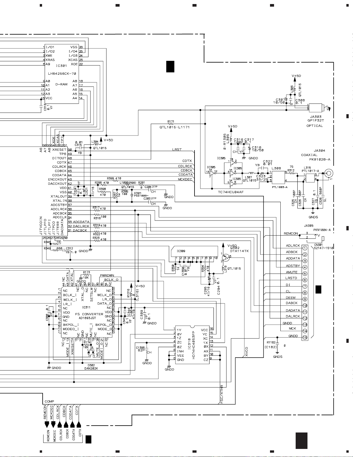
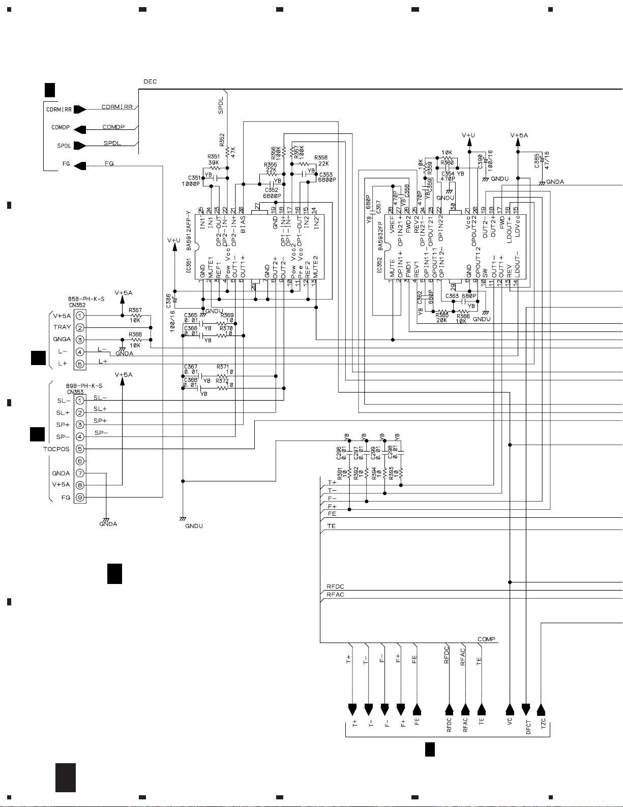
THIS MANUAL IS APPLICABLE TO THE
FOLLOWING MODEL(S) AND TYPE(S).
Type
KU/CA AC120V
MY AC220-230V
Model
CDR-850
Power Requirement Remarks
FOR U.S. MODELS
NECESSARY INFORMATION FOR DHHS
RULES MARKED ON THE REAR BASE AND ON
THE TOP OF CD MECHANISM AS BELOW.
DANGER – LASER RADIA TION WHEN OPEN.
AVOID DIRECT EXPOSURE TO BEAM.
Page 2
CDR-850
1. SAFETY INFORMATION
This service manual is intended for qualified service technicians ; it is not meant for the casual do-ityourselfer. Qualified technicians have the necessary test equipment and tools, and have been trained
to properly and safely repair complex products such as those covered by this manual.
Improperly performed repairs can adversely affect the safety and reliability of the product and may
void the warranty. If you are not qualified to perform the repair of this product properly and safely, you
should not risk trying to do so and refer the repair to a qualified service technician.
WARNING
This product contains lead in solder and certain electrical parts contain chemicals which are known to the state of California to cause
cancer, birth defects or other reproductive harm.
Health & Safety Code Section 25249.6 – Proposition 65
NOTICE
(FOR CANADIAN MODEL ONLY)
Fuse symbols (fast operating fuse) and/or (slow operating fuse) on PCB indicate that replacement parts must
be of identical designation.
REMARQUE
(POUR MODÈLE CANADIEN SEULEMENT)
Les symboles de fusible (fusible de type rapide) et/ou (fusible de type lent) sur CCI indiquent que les pièces
de remplacement doivent avoir la même désignation.
(FOR USA MODEL ONLY)
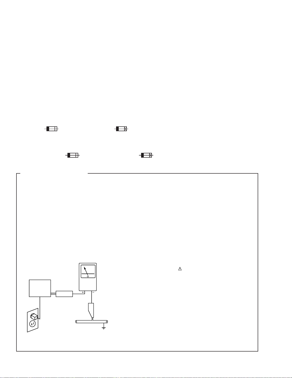
1. SAFETY PRECAUTIONS
The following check should be performed for the
continued protection of the customer and service
technician.
LEAKAGE CURRENT CHECK
Measure leakage current to a known earth ground (water
pipe, conduit, etc.) by connecting a leakage current tester
such as Simpson Model 229-2 or equivalent between the
earth ground and all exposed metal parts of the appliance
(input/output terminals, screwheads, metal overlays, control
shaft, etc.). Plug the AC line cord of the appliance directly
into a 120V AC 60Hz outlet and turn the AC power switch
on. Any current measured must not exceed 0.5mA.
Reading should
not be above
0.5mA
Earth
ground
Device
under
test
Also test with
plug reversed
(Using AC adapter
plug as required)
Leakage
current
tester
Test all
exposed metal
surfaces
ANY MEASUREMENTS NOT WITHIN THE LIMITS
OUTLINED ABOVE ARE INDICATIVE OF A POTENTIAL
SHOCK HAZARD AND MUST BE CORRECTED BEFORE
RETURNING THE APPLIANCE TO THE CUSTOMER.
2. PRODUCT SAFETY NOTICE
Many electrical and mechanical parts in the appliance
have special safety related characteristics. These are
often not evident from visual inspection nor the protection
afforded by them necessarily can be obtained by using
replacement components rated for voltage, wattage, etc.
Replacement parts which have these special safety
characteristics are identified in this Service Manual.
Electrical components having such features are identified
by marking with a
in this Service Manual.
The use of a substitute replacement component which does
not have the same safety characteristics as the PIONEER
recommended replacement one, shown in the parts list in
this Service Manual, may create shock, fire, or other hazards.
Product Safety is continuously under review and new
instructions are issued from time to time. For the latest
information, always consult the current PIONEER Service
Manual. A subscription to, or additional copies of, PIONEER
Service Manual may be obtained at a nominal charge from
PIONEER.
on the schematics and on the parts list
AC Leakage Test
2
Page 3
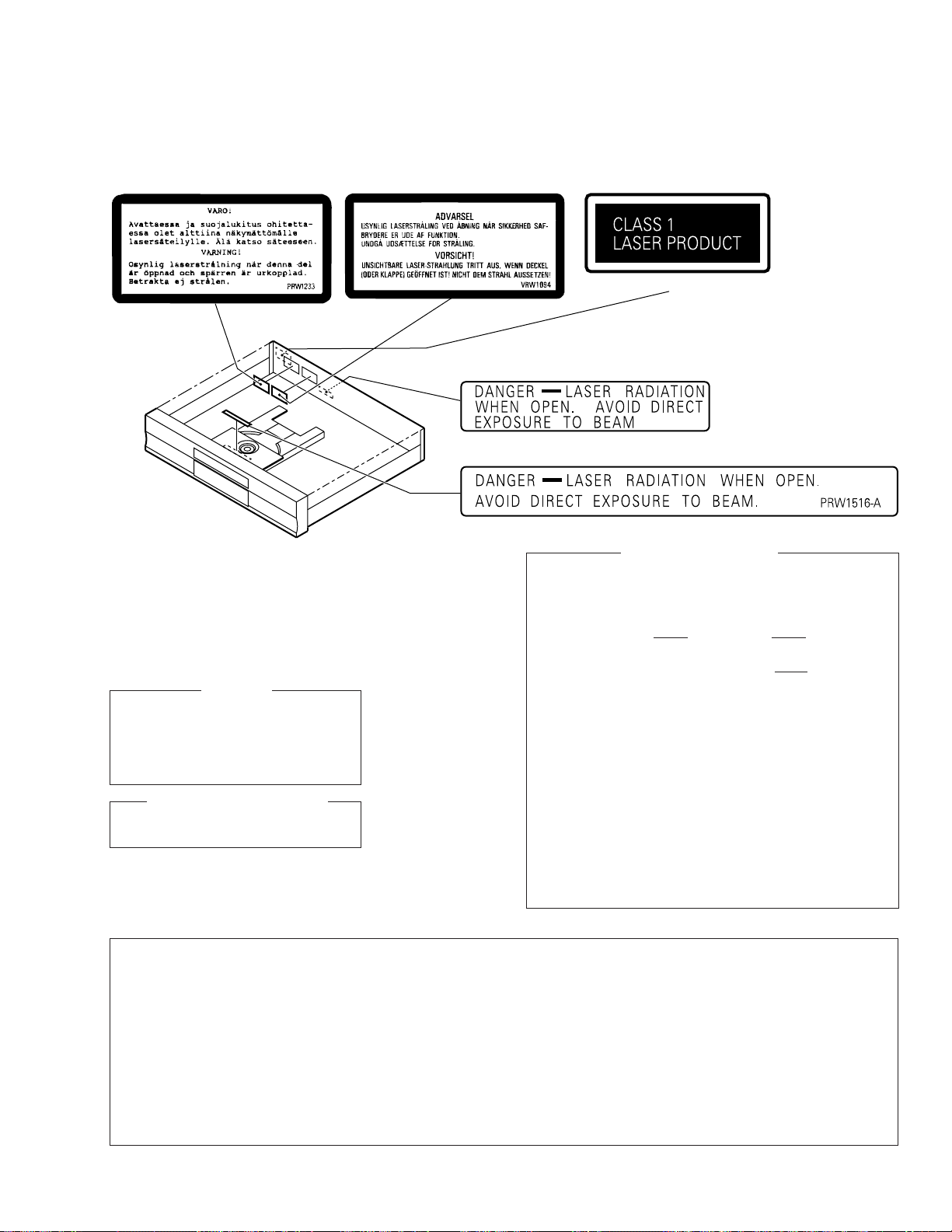
LABEL CHECK
KU/CA type
Printed on Rear Panel
Printed on Rear Panel
MY Type
MY Type MY Type
CDR-850
THIS PIONEER APPARATUS CONTAINS
LASER OF CLASS ΙΙΙ b.
SERVICING OPERATION OF THE APPARATUS
SHOULD BE DONE BY A SPECIALLY
INSTRUTED PERSON.
LASER DIODE CHARACTERISTICS
MAXIMUM OUTPUT POWER: 23 mW
WAVELENGTH: 778 – 787 nm
IMPORTANT
CONTENTS
1. SAFETY INFORMATION
2. EXPLODED VIEWS AND PARTS LIST
3. SCHEMATIC DIAGRAM
4. PCB CONNECTION DIAGRAM
5. PCB PARTS LIST
6. ADJUSTMENT
...............................................
....................................................
......................................
................
.....................................
..........................
Additional Laser Caution
1. Laser Interlock Mechanism
The position of the switch (S601) for detecting loading
state is detected by the system microprocessor, and the
design prevents laser diode oscillation when the switch
(S601) is not on CLMP terminal side (CLMP signal is OFF
or high level.). Thus, the interlock will no longer function if
the switch (S601) is deliberately set to CLMP terminal side
(low level).
The interlock also does not function in the test mode ∗.
Laser diode oscillation will continue, if pin 1 of M51593FP
(IC101) on the PRE-AMP BOARD ASSY mounted on the
pickup assembly is connected to GND, or pin 19 is
connected to low level (ON), or else the terminals of Q101
are shorted to each other (fault condition).
2. When the cover is opened with the servo mechanism
block removed and turned over, close viewing of the
objective lens with the naked eye will cause exposure to a
Class 1 laser beam.
∗ Refer to page 53.
2
7. GENERAL INFORMATION
4
7.1 PARTS
10
7.1.1 IC
34
7.1.2 DISPLAY
48
7.2 BLOCK DIAGRAM
53
7.3 DIAGNOSIS
.........................................................
...........................................................
................................................
................................................
................................
......................................
8. PANEL FACILITIES AND SPECIFICATIONS
....
59
59
59
74
76
78
83
3
Page 4
CDR-850
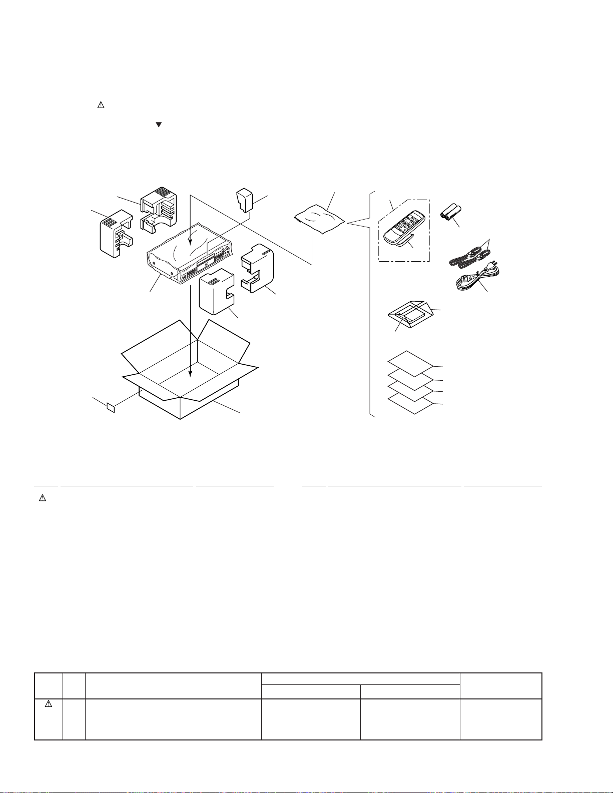
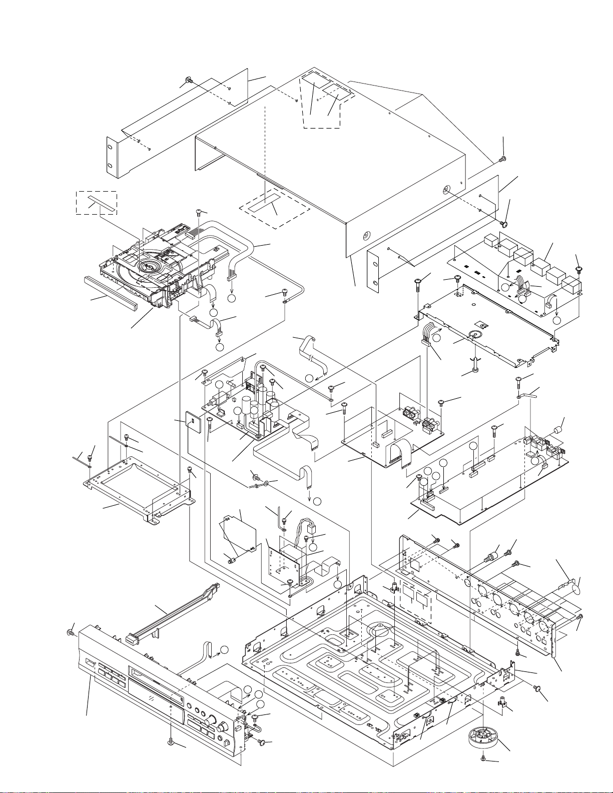
2. EXPLODED VIEWS AND PARTS LIST
NOTES:• Parts marked by "NSP" are generally unavailable because they are not in our Master Spare Parts List.
2.1 PACKING
The mark found on some component parts indicates the importance of the safety factor of the part.
•
Therefore, when replacing, be sure to use parts of identical designation.
Screws adjacent to mark on the product are used for disassembly.
•
12 (2/3)
12 (1/3)
13
2
(1) PACKING PARTS LIST
11 (1/2)
10
12 (3/3)
11 (2/2)
9
6
8
3
7
1
17
14
5
15
16
4
Mark No. Description Part No.
1 AC Power Cord See Contrast table (2)
2 Bar Code Label MY See Contrast table (2)
3 Audio Cable (L=1.2m) PDE1003
4 Operating Instructions PRE1282
(English/French/Spanish)
5 Caution PRM1045
6 Remote Control Unit PWW1122
(R-800)
7 Battery Cover PZN1010
NSP 8 Dry Cell Battery (R03,AAA) VEM-022
9 Polyethylene Bag RHL1024
10 Packing Case PHG2365
Mark No. Description Part No.
11 Protector (F) PHA1341
12 Protector (R) PHA1342
13 Seat RHX1006
NSP 14 CDR Disc PEX1007
NSP 15 Registration Card See Contrast table (2)
NSP 16 Brochure PEX1009
17 Polystylene cover PHL1067
(2) CONTRAST TABLE
CDR-850/MY and KU/CA are constructed the same except for the following :
Mark No. Symbol and Description
1 AC Power Cord DDG1072 DDG1028
2 Bar Code Label MY PRW1531 Not used
2 Bar Code Label KU Not used PRW1530
NSP 15
Registration Card PEX1010 PEX1008
4
CDR-850/MY CDR-850/KU/CA
Part No.
Remarks
Page 5
CDR-850
2.2 EXTERIOR SECTION
52
KU/CA
Type only
40
28
Refer to "2.4 LOADING
MECHANISM ASSY".
No Supplied
23
33
18
33
23
Part
11
31
C
B
D
34
33
59
14
3
45
42
39
KU/CA
Type only
8
12
I
7
5
60
10
E
48
12
J
50
14
4
12
H
11
25
24
D
KU/CA
43
Type only
56
11
15
K
47
20
12
34
2
A
24
9
J
11
1
13
49
11
C
I
B
F
11
51
53
46
52
41
11
K
34
A
IC308
19
6
G
L
34
14
22
L
26
57
Accessories for
the INPUT ASSY
58
36
30
Refer to "2.3 FRONT
PANEL SECTION".
27
55
37
MY
38
Type only
29
E
F
H
G
30
35
30
35
11
13
21
55
16
17
30
5
Page 6
CDR-850
(1) EXTERIOR SECTION PARTS LIST
Mark No. Description Part No. Mark No. Description Part No.
NSP 1 SERVO DIGITAL Assy See Contrast table (2)
2 AUDIO Assy See Contrast table (2)
3 POWER Assy See Contrast table (2)
NSP 4 TRANS Assy PWZ3752
5 Jumper Wire (J) D20PYY0335E
6 Connector Assy (8P) PDE1303
7 Connector Assy PG05KK-E10
8 Connector Assy PG09KK-E35
9 Power Transformer See Contrast table (2)
10 Fuse (FU1) See Contrast table (2)
11 Screw (Steel) ABA1011
12 Screw (Steel) ABA1207
NSP 13 PCB Mould AMR1525
NSP 14 Cord Stopper DNF1128
15 Bonnet PYY1267
NSP 16 Under Base PNA2484
17 Rear Base See Contrast table (2)
NSP 18 Mecha Base PNB1591
19 Terminal Screw AKE-031
20 Connector Assy (8P) PDE1304
21 Insulator AMR7198
NSP 22 Cap VEC1810
23 Cord Clamper RNH-184
24 Screw RBA1132
NSP 25 Lead Wire Unit PDF1195
26 Connector Assy PF03PP-C16
27 Power Button PAC1918
28 Tray Panel PNW2902
29 Screw BBZ30P080FCC
30 Screw IBZ30P060FCC
31 Screw BBZ30P100FCC
32 • • • • •
33 Screw PBA1112
34 Screw IBZ30P180FCC
35 Binder PEC-107
36 Black Label PRW1470
37 Caution Label HE See Contrast table (2)
38 Caution Label See Contrast table (2)
39 65 Label See Contrast table (2)
NSP 40 Laser Caution Label See Contrast table (2)
41 INPUT Assy See Contrast table (2)
42 FCC Label See Contrast table (2)
43 DOC Label See Contrast table (2)
44 • • • • •
45 Rack Angle L PNB1604
46 Rack Angle R PNB1605
NSP 47 I/O Angle PNB1607
NSP 48 Transformer Cover PNM1338
NSP 49 Card Spacer QEC1012
50 Screw RBA1128
51 Screw BBZ40P080FCC
52 Screw BBZ40P140FZK
53 Screw IBP30P090FCC
54 • • • • •
55 Screw IBZ30P080FZK
56 Screw IBZ30P200FMC
57 Screw PMZ26P040FMC
58 Screw PMZ30P060FCC
59 Rivet RBM-003
60 Fuse Cover PNM1343
(2) CONTRAST TABLE
CDR-850/MY and KU/CA are constructed the same except for the following :
Mark No. Symbol and Description
NSP 1 SERVO DIGITAL Assy PWM2219 PWM2220
2 AUDIO Assy PWZ3933 PWZ3934
3 POWER Assy PWZ3937 PWZ3938
9 Power Transformer PTT1346 PTT1355
10 Fuse (FU1 : T500mA) AEK1051 Not used
10 Fuse (FU1 : 1A) Not used REK1075
17 Rear Base PNA2488 PNA2482
37 Caution Label HE PRW1233 Not used
38 Caution Label VRW1094 Not used
39 65 Label Not used ARW7050
NSP 40 Laser Caution Label Not used PRW1516
41 INPUT Assy PWZ3929 PWZ3930
42 FCC Label Not used VRW1725
43 DOC Label Not used VRW1726
CDR-850/MY CDR-850/KU/CA
6
Part No.
Remarks
Page 7
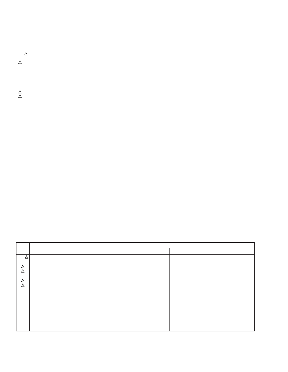
2.3 FRONT PANEL SECTION
CDR-850
23
16
12
8
23
7
17
15
13
14
Accessories for the
VR ASSY.
1
19
20
11
A
21
23
26
6
4
10
9
18
22
A
5
2
23
3
FRONT PANEL SECTION PARTS LIST
•
Mark No. Description Part No. Mark No. Description Part No.
NSP 2 HEADPHONE Assy PWZ3715
1 FUNCTION Assy PYY1266
NSP 3 VR Assy PWZ3719
4 22P F•F•C/60V PDD1190
5 Screw With Washer ABA1005
6 HP Knob H PAC1944
7 Mode Button H PAC1945
8 Manual Button H(L) PAC1946
9 REC Button H PAC1948
10 Cord Clamper RNH-184
11 Manual Button H(R) PAC1947
12 VOL Knob Assy PXA1621
13 REC Knob H L PAC1942
14 REC Knob H R PAC1943
15 FL Sheet PAM1762
16 Display Window H PAM1794
17 LED Lens PNW2745
18 REC Ring PNW2795
19 Lens PNW2796
20 Sub Panel PNW2797
21 Front Panel H PNW2903
22 Play Button H PAC1950
23 Screw PPZ30P100FMC
24 • • • • •
25 • • • • •
26 IC (EEPROM) PYY1250
7
Page 8
CDR-850
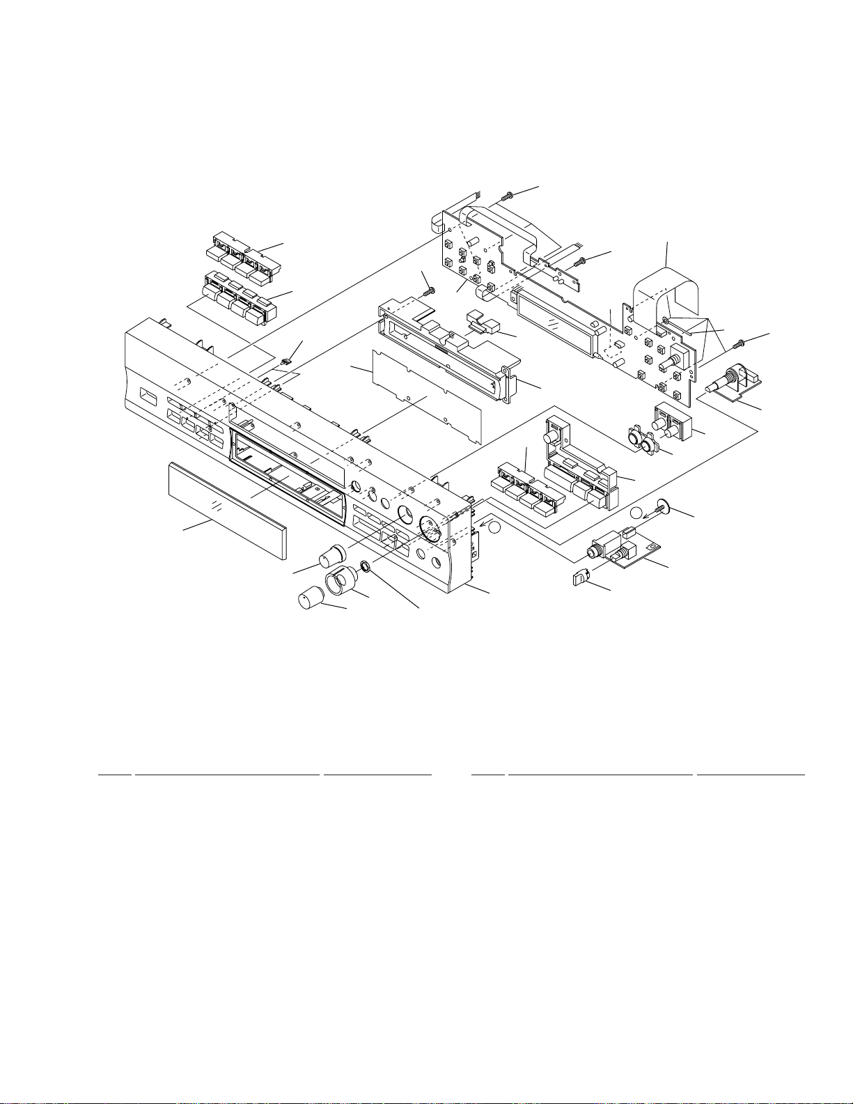
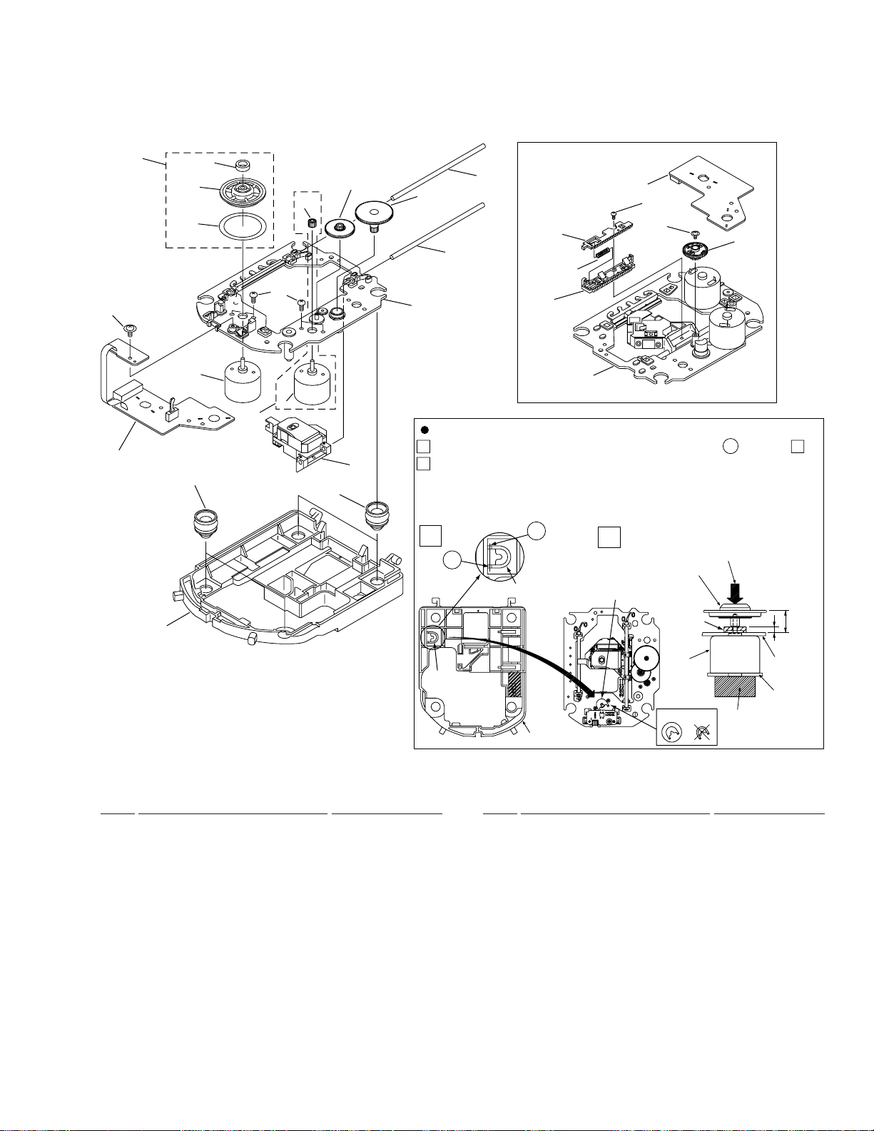
2.4 LOADING MECHANISM ASSY
• Bottom View
20
9
26
24
23
30
26
27
A
13
12
Loading Base
25
7
21
6
4
3
28
A
15
14
19
1
29
22
5
2
31
5
18
11
16
17
8
LOADING MECHANISM ASSY PARTS LIST
•
10
Mark No. Description Part No. Mark No. Description Part No.
NSP 2 Earth Lead Unit PDF1088
1 32P F•F•C/30V PDD1187
3 Connector Assy PG02KK-E35
4 DC Motor PXM1027
5 Screw DBA1006
6 Motor Pulley PNW1634
7 Screw VBA1055
8 Tray Stopper Spring VBH1277
9 Rubber Belt VEB1260
10 Loading Base VNL1730
11 Tray VNL1731
12 Gear Pulley VNL1733
13 Loading Gear VNL1734
14 Drive Gear VNL1735
15 Drive Cam VNL1736
NSP 18 CD-RW SERVO MECH Assy PXA1609
NSP 22 Loading Mechanism Assy PXA1608
NSP 27 LOADING A Assy PWZ3727
NSP 28 LOADING B Assy PWZ3728
16 Lock Plate VNL1820
17 Tray Stopper VNL1739
19 Screw BBZ26P040FMC
20 Screw IPZ20P080FMC
21 Loading Motor Assy VXX2505
23 Clamper Plate VNE2068
24 Bridge VNE2069
25 Clamper VNL1738
26 Screw IPZ26P060FMC
29 Tray Holder PNM1341
30 Spacer PNM1334
31 Stopper DNH2076
8
Page 9
2.5 SERVO MECHANISM ASSY
CDR-850
22
25
15
20
10
9
7
23
2
3
26
11
16
19
18
• Bottom View
SERVO MECH ASSY
14
6
13
Carriage Base S
24
22
12
How to Install the Disc Table
1
1
4
21
5
Use nippers or other tool to cut the two sections marked A in figure
2
While supporting the spindle motor shaft with the stopper, put spacer on
top of the carriage base, and stick the disc table on top (takes about 9kg
pressure). Take off the spacer.
1
A
A
Spacer
2
Spacer setting
Position
(Pressure of about 9kg)
Disc table Assy
1
.
8
SERVO MECHANISM ASSY PARTS LIST
•
Spacer
Servo Base
Spacer
Spindle
motor
OK NG
Stopper
Mark No. Description Part No. Mark No. Description Part No.
NSP 1 SERVO MECH Assy PWZ3758
2 D.C.mortor Assy PEA1235
NSP 3 DC Motor PXM1042
4 Float Rubber A AEB7063
5 Float Rubber B AEB7066
NSP 6 Rack Spring DBH1285
NSP 7 Mirror Sheet PNM1325
8 Servo Base PNW2853
9 Pinion Gear PNW2854
10 Gear A PNW2855
11 Gear B PNW2856
12 Gear C PNW2857
13 Rack PNW2858
14 Rack Stopper PNW2859
NSP 15 Disc Table PNW2860
NSP 20 Magnet VYM1024
16 Carriage Base S PNW2874
17 • • • • •
18 Guide Bar VLL1488
19 Sub Guide Bar VLL1489
21 CD-R Pickup PEA1351
22 Screw IPZ20P060FMC
23 Screw PMZ20P030FMC
24 Screw JGZ17P030FMC
25 Disc Table Assy PEA1349
26 Carriage Motor Assy PEA1350
11mm
2.8mm
Carriage
Base
PCB
9
Page 10
1
23
4
CDR-850
3. SCHEMATIC DIAGRAM
3.1 OVERALL CONNECTIONS, LOADING A, B, and SERVO MECH ASSEMBLIES
A
CD-R PICUP ASSY
PEA1351
B
C
SERVO
MECH ASSY
(PWZ3758)
PEA1350
PEA1235
D
SERVO DIGITAL ASSY
(PWM2219 : MY)
(PWM2220 : KU/CA)
D
1/6
D
6/6
B
LOADING B
C
ASSY
(PWZ3728)
VXX2505
PC651
NJL5803K–F1
LOADING A ASSY
A
(PWZ3727)
D
LOADING MECH ASSY (PXA1608)
10
A
B C
1234
FUNCTION ASSY
J
(PWZ3699)
Page 11
5
678
CDR-850
Note : When ordering service parts, be sure to refer to "EXPLODED VIEWS and P AR TS LIST" or "PCB PARTS LIST".
F
HEADPHONE
ASSY
E
E
AUDIO ASSY
(PWZ3933: MY)
(PWZ3934: KU/CA)
1/2,
E
2/2
(PWZ3715)
A
B
H
TRANS ASSY
I
(PWZ3752)
POWER ASSY
(PWZ3937: MY)
(PWZ3938: KU/CA)
POWER TRANSFORMER
AC POWER CORD
DDG1072 : MY TYPE
DDG1028 : KU/CA TYPE
K
INPUT ASSY
(PWZ3929: MY)
(PWZ3930: KU/CA)
VR ASSY
G
(PWZ3719)
C
D
11
5
6
7
8
Page 12
1
CDR-850
3.2 SERVO DIGITAL ASSY(1/6)
A
2/6
D
B
23
5/6
D
4
4/6
D
2/6
D
ATIP DECODER
C
3/6
D
D
12
1/6
D
1234
Page 13
5
678
CDR-850
8BIT LATCH
MECH.CONTROL MICOM BLOCK
D
SERVO DIGITAL ASSY(1/6)
1/6
(PWM2219 : MY)
(PWM2220 : KU/CA)
•
MECH. CONTROL MICOM BLOCK
D
A
4/6
B
C
6/6
D
CN701
J
1/6
D
5
6
7
8
13
D
Page 14
1
23
CDR-850
3.3 SERVO DIGITAL(2/6) and PICKUP ASSEMBLIES
4
D
A
CD-R PICUP ASSY
PEA1351
B
SERVO DIGITAL ASSY(2/6)
2/6
(PWM2219 : MY)
(PWM2220 : KU/CA)
•
RF PROCESSOR BLOCK
C
D
14
2/6
D
1234
Page 15
5
678
CDR-850
A
3/6
D
5/6
D
B
MY TYPE
ONLY
D
4/6
D
D
D
3/6
1/6
6/6
C
D
2/6
D
5
6
7
8
15
Page 16
1
CDR-850
3.4 SERVO DIGITAL ASSY(3/6)
A
2/6
D
1/6
D
B
23
4
5/6
D
C
2/6
D
D
16
3/6
D
1234
Page 17
5
678
CDR-850
A
1/6
D
D
SERVO DIGITAL ASSY(3/6)
3/6
(PWM2219 : MY)
(PWM2220 : KU/CA)
•
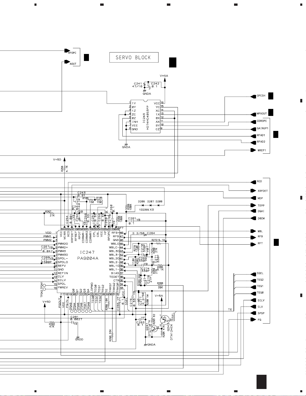
SERVO BLOCK
D
D
6/6
1/6
D
2/6
B
CDR SERVO AMP
5
1/6
D
3/6
D
6
7
8
17
C
D
Page 18
1
CDR-850
3.5 SERVO DIGITAL ASSY(4/6)
6/6
D
A
B
23
4
INPUT
CN3002
K
C
INPUT
D
1/6
18
4/6
D
1234
D
Page 19
5
678
CDR-850
A
D
SERVO DIGITAL ASSY(4/6)
4/6
(PWM2219 : MY)
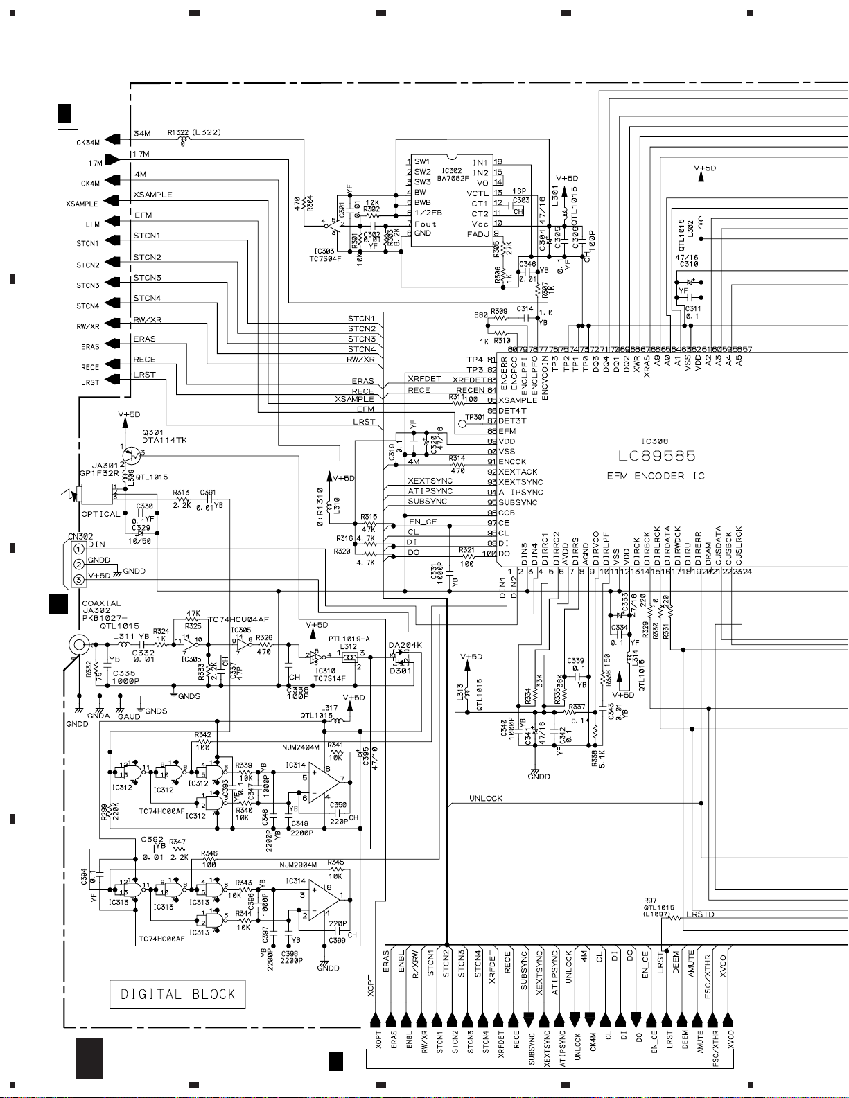
(PWM2220 : KU/CA)
•
DIGITAL BLOCK
OUTPUT
OUTPUT
B
C
1/2
E
J801
D
5/6
D
5
6
7
D
4/6
8
19
Page 20
1
CDR-850
3.6 SERVO DIGITAL ASSY(5/6)
3/6
D
A
B
23
4
CN501
A
CN601
C
C
D
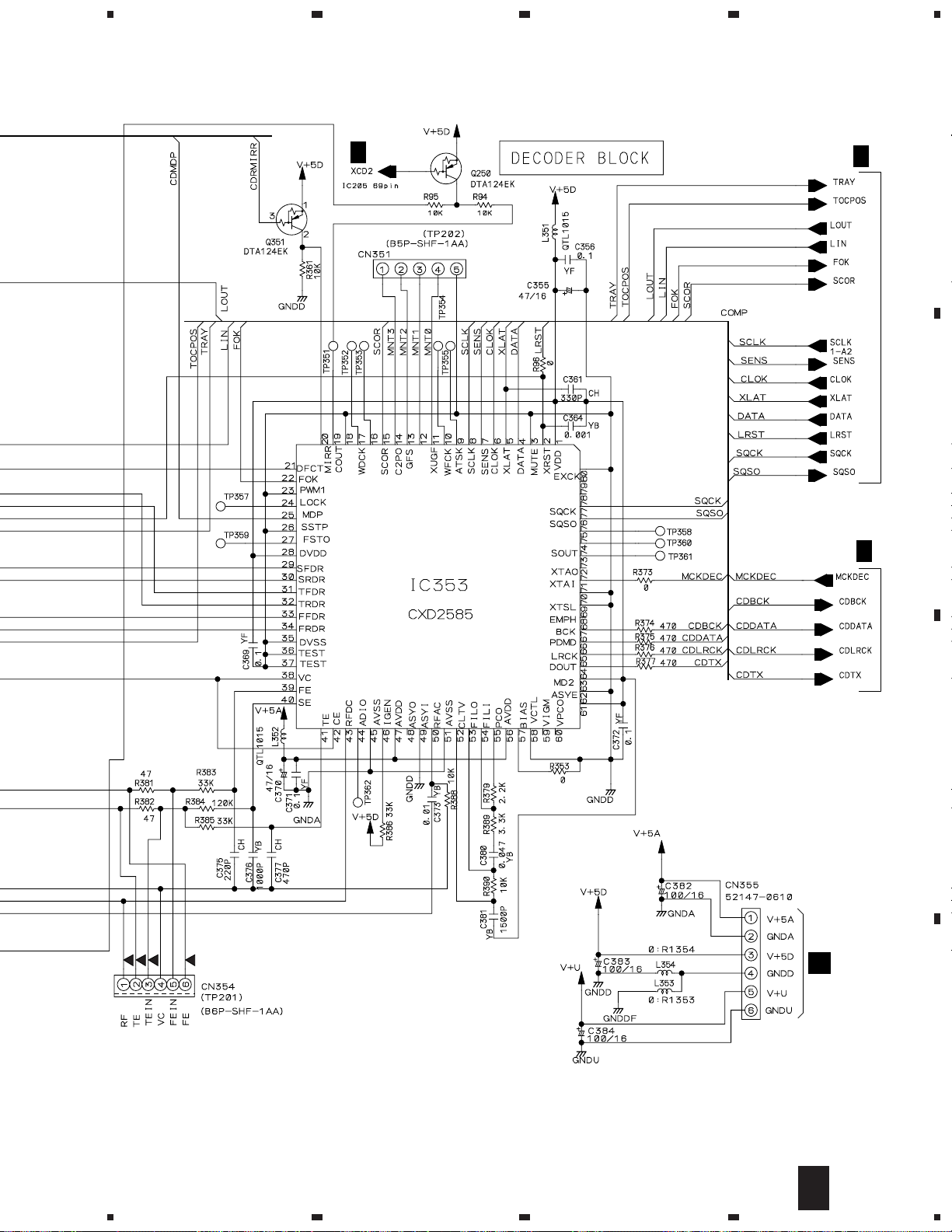
SERVO DIGITAL ASSY(5/6)
5/6
(PWM2219 : MY)
(PWM2220 : KU/CA)
•
DECODER BLOCK
D
2/6
D
20
5/6
D
1234
Page 21
5
6
678
CDR-850
1/6
D
D
1/6
A
B
H
J21
D
4/
C
D
5/6
D
5
6
7
8
21
Page 22
1
23
CDR-850
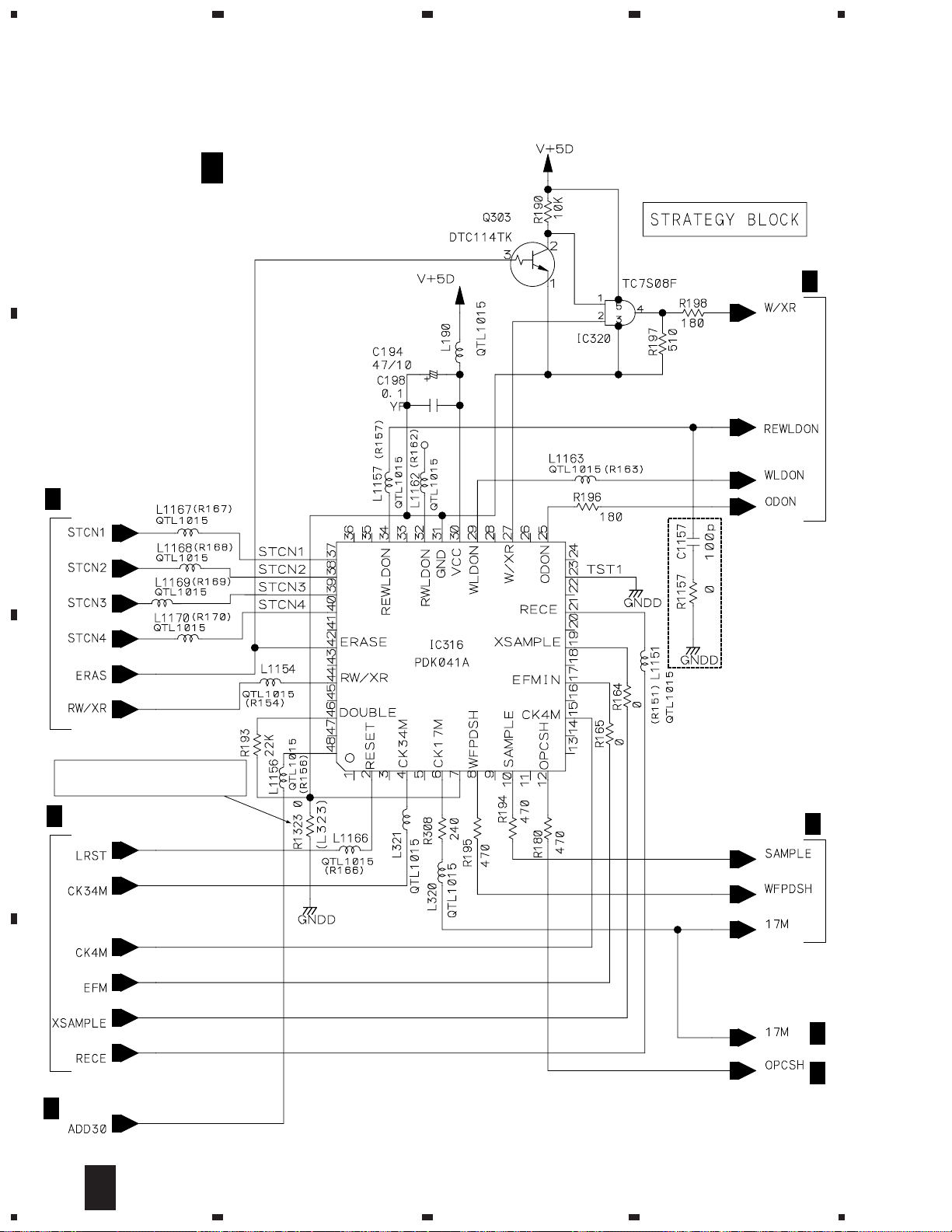
3.7 SERVO DIGITAL ASSY(6/6)
4
A
D
B
4/6
D
SERVO DIGITAL ASSY(6/6)
6/6
(PWM2219 : MY)
(PWM2220 : KU/CA)
•
STRATEGY BLOCK
KU/CA TYPE
ONLY
D
2/6
C
D
R1323 : 0 (MY TYPE)
L323 : QTL1015 (KU/CA TYPE)
4/6
D
1/6
D
22
6/6
D
1234
D
D
D
2/6
4/6
3/6
Page 23

CDR-850
23
Page 24
1
23
CDR-850
3.8 AUDIO(1/2) and HEADPHONE ASSEMBLIES
A
CN301
4/6
D
4
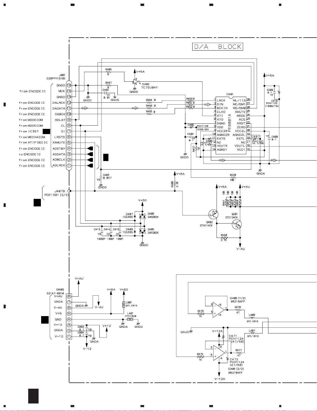
D/A CONVERTER
B
CN8101
E
2/2
K
C
J31
H
D
24
1/2
E
1234
Page 25
5
678
CDR-850
E
AUDIO ASSY(1/2)
1/2
(PWZ3933 : MY)
(PWZ3934 : KU/CA)
• D/A BLOCK
CN8101,
CN8102
K
A
B
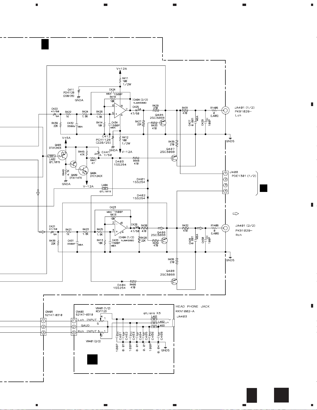
HEADPHONE ASSY
F
(PWZ3715)
: AUDIO SIGNAL
ROUTE
C
D
1/2
E
5
6
7
F
8
25
Page 26
1
23
CDR-850
3.9 AUDIO(2/2) and VR ASSEMBLIES
A
4
B
C
CN8004
K
VR ASSY
G
(PWZ3719)
CN8005
K
D
26
2/2
E
1234
G
Page 27
5
678
CDR-850
A
: AUDIO SIGNAL ROUTE
A/D CONVERTER
E
1/2
E
AUDIO ASSY(2/2)
2/2
(PWZ3933 : MY)
(PWZ3934 : KU/CA)
•
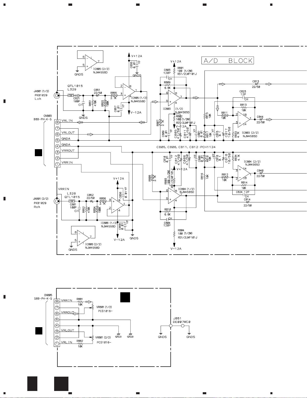
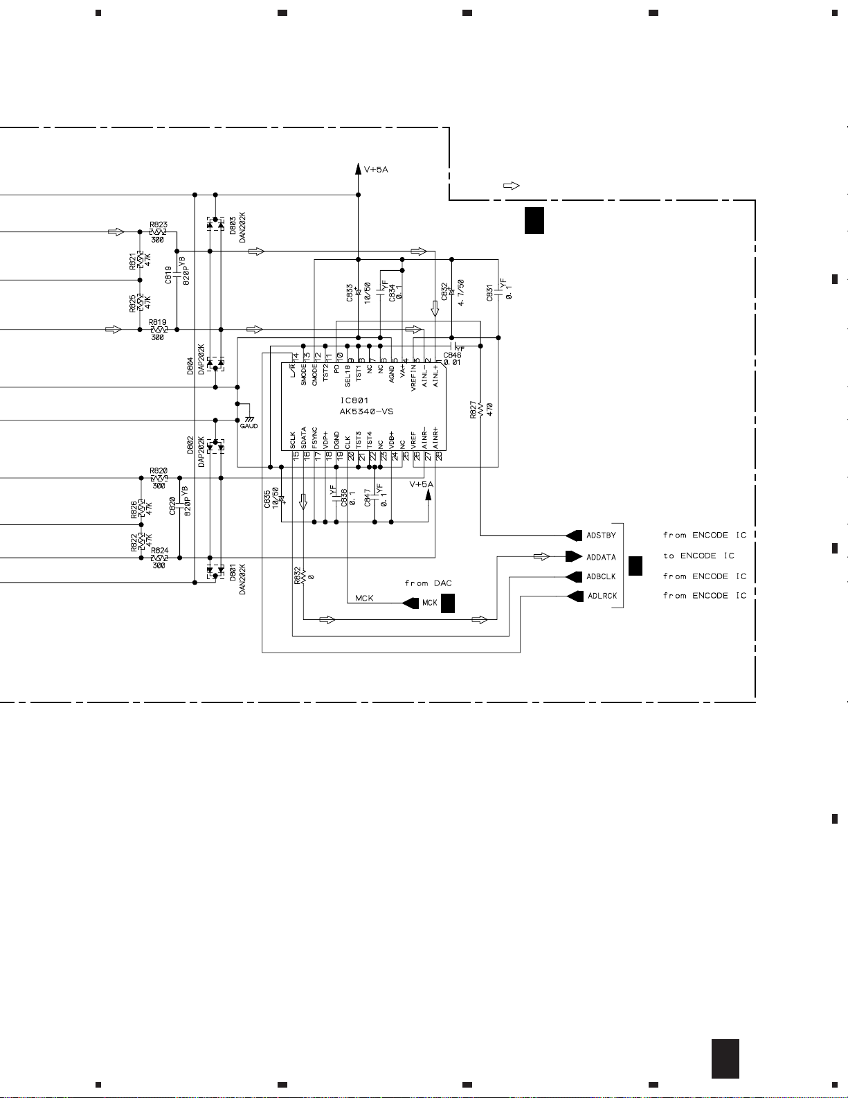
A/D BLOCK
1/2
E
B
C
D
2/2
E
5
6
7
8
27
Page 28

1
23
CDR-850
3.10 POWER and TRANS ASSEMBLIES
A
AC POWER
CORD
(10000p/250)
B
1P AC INLET
• NOTE FOR FUSE REPLACEMENT
(10000p/250)
(10000p/250)
4
POWER TRANSFORMER
C901
C902
C903
C904
C905
C906
C
C909
C907
C908
TRANS ASSY
I
(PWZ3752)
D
28
H
I
1234
Page 29

5
678
CDR-850
A
POWER ASSY
H
(PWZ3937 : MY)
(PWZ3938 : KU/CA)
J701
J
B
CAUTION : FOR CONTINUED PROTECTION AGAINST
RISK OF FIRE. REPLACE ONLY WITH
SAME TYPE NO. ICP-N15, MFD BY ROHM
CO., LTD. FOR IC22,IC23,IC25.
1/2
E
CN402
CN8003
K
5/6
D
CN355
C
D
H
5
6
7
8
29
Page 30

1
CDR-850
3.11 FUNCTION ASSY
23
4
A
REMOTE
RECEIVER
UNIT
FL HOLDER
J
FUNCTION ASSY
FUNCTION ASSY
S702 : PLAY 3
S703 : PAUSE 8
B
GNDS
H
CN51
V–27
AC2
AC1
S704 : STOP 7
S705 : TRACK SEARCH 4 1
S706 : TRACK SEARCH ¡ ¢
S707 : OPEN/CLOSE
S708 : TIME/MARGIN
S709 : RECORD
S710 : DIGITAL SYNCHRO
S711 : REC MUTE
S712 : SKIP ID SET
S713 : SKIP ID CLEAR
S714 : SKIP PLAY
S715 : MENU
S716 : TRACK No. AUTO/MANUAL
S717 : TRACK No. WRITE
S718 : FINALIZE
S719 : ERASE
(PWZ3699)
C
S712–S719 : VSG1009
D
CN8006
K
30
J
1234
Page 31

5
678
CDR-850
A
CN202
1/6
D
B
R710–R715 :
ACN7081
MODE CONTROLLER
SYSTEM
RESET
Q701–Q704 :
DTA114EK
C
D
J
5
6
7
8
31
Page 32

1
CDR-850
3.12 INPUT ASSY
A
B
23
4
CN805
G
CN803
2/2
E
J32
H
J708
J8006
J
K
C
D
32
K
1234
Page 33

K
J8006
5
678
CDR-850
K
INPUT ASSY
(PWZ3929 : MY)
(PWZ3930 : KU/CA)
A
B
1/2
E
J407,
J408
E
J408
1/2
C
4/6
D
CN302
D
K
5
6
7
8
33
Page 34

CDR-850
4. PCB CONNECTION DIAGRAM
NOTE FOR PCB DIAGRAMS :
1. Part numbers in PCB diagrams match those in the schematic
diagrams.
2. A comparison between the main parts of PCB and schematic
diagrams is shown below.
Symbol In PCB
Diagrams
BCE
BCE
D
Symbol In Schematic
Diagrams
BCEBCE
BCE
DGGSS
BCE
DGS
Part Name
Transistor
Transistor
with resistor
Field effect
transistor
Resistor array
3. The parts mounted on this PCB include all necessary parts for
several destinations.
For further information for respective destinations, be sure to
check with the schematic diagram.
4. View point of PCB diagrams.
Connector
Capacitor
SIDE A
P.C.Board
Chip Part
SIDE B
3-terminal
regulator
34
Page 35

1
234
4.1 LOADING A, LOADING B and SERVO MECH ASSEMBLIES
CDR-850
A
SIDE A
A
LOADING A ASSY
D
CN352
B
LOADING
B ASSY
SIDE B
B
M
(PNP1447-B)
D
CN353
C
SERVO MECH
ASSY
C
M
M
D
(PNP1447-B)
BA
1
2
3
C
4
35
Page 36

1
1
C
C
CDR-850
4.2 SERVO DIGITAL ASSY
A
C
CN601
23
A
CN501
PICKUP
ASSY
D
SERVO DIGITAL
ASSY
4
H
J2
B
J
CN701
C
VR101 VR107
VR108
VR103
IC351 Q107
IC352
VR104
VR106
VR102
VR105
Q102 IC243
Q101Q106 IC103 IC101
IC355
Q250IC206
IC248
IC249
IC247
IC245
IC212
IC250
IC213
Q243
Q244
IC211 IC209
I
I
SIDE A
D
36
D
1234
Page 37

H
0
J21
E
5
J801
678
CDR-850
A
K
CN3002
B
C
VR301
IC201 IC302 IC310IC309
IC205 IC204 IC303 IC202 IC314 Q301IC316
9
IC353 IC301 IC308 IC311 IC318
Q203
5
6
7
(PNP1445-G)
D
8
D
37
Page 38

A
B
1
CDR-850
23
D
SERVO DIGITAL ASSY
4
C
(PNP1445-G)
IC305 Q302 IC354 Q351
IC312 Q204 IC207 IC203
Q201IC313 IC320 Q303
SIDE B
D
38
D
1234
Page 39

5
678
CDR-850
A
B
IC246 IC105Q242
IC210 IC208
5
Q241
Q103
6
Q104 Q105Q201 IC102 IC104
C
D
D
7
8
39
Page 40

1
23
CDR-850
4.3 AUDIO, HEADPHONE and VR ASSEMBLIES
CN8101
K
CN8102
A
Q407
Q408
Q406
Q405
IC803
IC804
IC404
B
4
G
VR ASSY
(PNP1456-D)
K
CN8005
K
CN8004
H
J31
D
CN301
C
IC451
(PNP1463-B)
E
AUDIO ASSY
K
CN8101
D
SIDE A
40
E
F
1234
G
HEADPHONE
F
ASSY
(PNP1456-D)
Page 41

G
VR ASSY
(PNP1456-D)
1
234
CDR-850
E
AUDIO ASSY
A
Q404
Q409
Q403
IC406
B
HEADPHONE
F
ASSY
IC401
IC801
Q401
IC402
Q402
C
(PNP1463-B)
(PNP1456-D)
1
D
SIDE B
FE
2
3
G
4
41
Page 42

1
23
CDR-850
4.4 POWER and TRANS ASSEMBLIES
4
AC POWER CORD
H
A
LIVENEUTRAL
B
POWER ASSY
K
CN8003
E
CN402
IC37
IC33
IC36
IC32
IC31
IC35
D
CN355
IC25
IC21
IC23
IC24
(PNP1463-B)
J
C
J701
SIDE A
D
I
42
H
I
1234
POWER
TRANSFORMER
TRANS ASSY
(PNP1456-D)
Page 43

1
234
CDR-850
H POWER ASSY
A
B
SIDE B
(PNP1463-B)
C
I TRANS ASSY
D
(PNP1456-D)
43
H
1
2
3
I
4
Page 44

1
CDR-850
4.5 FUNCTION ASSY
J
A
B
23
FUNCTION ASSY
4
D
SIDE A
IC705
J
FUNCTION ASSY
C
CN202
Q705 IC702
D
IC701
44
SIDE B
J
1234
Page 45

5
678
CDR-850
H
CN51
A
B
K
(PNP1456-D)
CN8006
C
D
IC704
Q701 Q704Q706
J
5
6
7
8
45
Page 46

1
CDR-850
4.6 INPUT ASSY
A
23
K INPUT ASSY
4
IC3001
Q408
D CN302
G CN805
B
Q8009
Q8010
E CN803
J J708
H J32
C
D
Q8101
Q8102
J407,
E
J408
E J408
SIDE A
46
K
1234
(PNP1463-B)
Page 47

1
234
CDR-850
K
INPUT ASSY
A
Q8002
Q8004
Q8007
Q8003
Q8006
Q8005
IC8001
IC8003
Q8202
Q8201
IC8101
IC8103
IC8105
Q8103
B
C
IC8102
IC8104
IC8106
Q8104
Q3705
Q3706
Q3707
Q3708
Q3701
Q3702
Q3703
Q3704
(PNP1463-B)
1
2
3
SIDE B
K
4
47
D
Page 48

CDR-850
Mark No. Description Part No.
Mark No. Description Part No.
5. PCB PARTS LIST
NOTES:•Parts marked by "NSP" are generally unavailable because they are not in our Master Spare Parts List.
The mark found on some component parts indicates the importance of the safety factor of the part.
•
Therefore, when replacing, be sure to use parts of identical designation.
When ordering resistors, first convert resistance values into code form as shown in the following examples.
•
Ex.1 When there are 2 effective digits (any digit apart from 0), such as 560 ohm and 47k ohm (tolerance is shown by J=5%,
and K=10%).
Ex.2 When there are 3 effective digits (such as in high precision metal film resistors).
560 Ω→56 × 10
47k Ω→47 × 103→ 473 ........................................................ RD1/4PU 4 7 3 J
0.5 Ω→R50 .....................................................................................RN2H
1 Ω→1R0 .....................................................................................RS1P
5.62k Ω→ 562 × 10
LIST OF WHOLE PCB ASSEMBLIES
Mark Symbol and Description
NSP SERVO MECH ASSY PWX1569 PWX1569
NSP LOADING A ASSY PWZ3727 PWZ3727
NSP LOADING B ASSY PWZ3728 PWZ3728
NSP SERVO MECH ASSY PWZ3758 PWZ3758
NSP
SERVO DIGITAL ASSY PWM2219 PWM2220
1
→ 561 ........................................................ RD1/4PU 5 6 1 J
R 5 0
1 R 0
1
→ 5621 ...................................................... RN1/4PC 5 6 2 1 F
Part No.
MY Type KU/CA Type
K
K
Remarks
NSP
NSP
Mark No. Description Part No. Mark No. Description Part No.
A
SWITCH
OTHERS
B
OTHERS
C
SEMICONDUCTORS
POWER AUDIO I/O ASSY PWX1600 PWX1601
INPUT ASSY PWZ3929 PWZ3930
AUDIO ASSY PWZ3933 PWZ3934
POWER ASSY PWZ3937 PWZ3938
FUNCTION ASSY PWX1595 PWX1595
NSP FUNCTION ASSY PWZ3699 PWZ3699
NSP HEADPHONE ASSY PWZ3715 PWZ3715
NSP VR ASSY PWZ3719 PWZ3719
NSP TRANS ASSY PWZ3752 PWZ3752
LOADING A ASSY
S501 VSK1011
CN502 KR CONNECTOR S2B-PH-K-S
CN501 KR CONNECTOR S5B-PH-K-S
SWITCHES AND RELAYS
S601 PSG1013
RESISTORS
All Resistors RD1/4PU J
OTHERS
J601 3P JUMPER WIRE D20PWW0305E
CN601 KR CONNECTOR S9B-PH-K-S
LOADING B ASSY
SERVO DIGITAL ASSY
D
CN551 KR CONNECTOR B2B-PH-K-S
SERVO MECH ASSY
PC651 NJL5803K-F1
(1) CONTRAST TABLE
PWM2220 and PWM2219 are constructed the same except
for the following :
Mark Symbol and Description
L323 Not used QTL1015
C1157 Not used
R1157 Not used RS1/10S0R0J
R1181,R1323 RS1/10S0R0J Not used
PWM2219 PWM2220
Part No.
CCSQCH101J50
Remarks
48
Page 49

CDR-850
Mark No. Description Part No.
(2) PARTS LIST FOR PWM2219
SEMICONDUCTORS
IC311 AD1893JST
IC103 AK8563
IC201 BA05T
IC351 BA5912AFP-Y
IC352 BA5932FP
IC302 BA7082F
IC353 CXD2585Q
IC104, IC105, IC243, IC318 HD74HC4053FP
IC203 HD74HC573FP
IC308 LC89585
IC301 LH64256CK-70
IC212 LP2950CZ-5.0(NS)
IC245 M5238AFP
IC102 MC34072D
IC246 NJM2100M
IC250 NJM2107F
IC101 NJM2136M
IC207, IC248, IC249, IC314 NJM2904M
IC247 PA9004A
IC309 PCX1021
IC205 PDJ014A
IC316 PDK041A
IC204 PE5073A9
IC206 PST994C
IC202 TC4W53F
IC312, IC313 TC74HC00AF
IC305 TC74HCU04AF
IC210 TC7S00F
IC208, IC303 TC7S04F
IC320 TC7S08F
IC209, IC211, IC310 TC7S14F
IC355 TK11041M-1
Q302 DTA114EK
Q102, Q301 DTA114TK
Q242, Q351 DTA124EK
Q250 DTA124TK
Q103, Q104, Q241, Q243, Q244 DTC114TK
Q303 DTC114TK
Q101, Q107, Q201, Q203, Q204 DTC124EK
D101, D103–D105, D110 1SS355
D201, D202, D205–D210 1SS355
D214, D215 1SS355
D211, D301 DA204K
D302 DAN202K
D203 DAP202K
D102, D212 MA704
COILS AND FILTERS
L209 OTL1040
L308 PULSE TRANS. PTL1003
L315 CHOKE COIL PTL1017
L312 EMI FILTER PTL1019
L1097, L1098, L1151, L1154 QTL1015
L1156, L1157, L1162, L1163 QTL1015
L1166–L1171, L190, L201, L202 QTL1015
L211–L222, L301–L304, L307 QTL1015
L309 CHIP SOLID INDUCTOR QTL1015
L311 CHIP SOLID INDUCTOR QTL1015
Mark No. Description Part No.
L313, L314, L317, L318 QTL1015
L320, L321, L351, L352 QTL1015
CAPACITORS
C120 CCSQCH100D50
C306, C316, C325, C326, C338 CCSQCH101J50
C303 CCSQCH160J50
C350, C375, C399 CCSQCH221J50
C203, C204, C278 CCSQCH270J50
C133, C361 CCSQCH331J50
C337 CCSQCH470J50
C231, C377 CCSQCH471J50
C134 CCSQCH6R0D50
C1188 CCSQCH681J50
C1395 CCSQCH820J50
C104 CCSQCJ3R0C50
C328 CCSQSL561J50
C232, C307, C318, C329 CEAT100M50
C103 CEAT101M10
C102, C150, C382–C384, C386 CEAT101M16
C390 CEAT101M16
C214, C255 CEAT1R0M50
C206, C212 CEAT221M6R3
C264, C277 CEAT2R2M50
C323 CEAT330M25
C223 CEAT3R3M50
C108, C194, C395 CEAT470M10
C149, C209, C226, C241, C248 CEAT470M16
C275, C279, C295, C304, C310 CEAT470M16
C320, C321, C333, C341, C344 CEAT470M16
C355, C370, C385 CEAT470M16
C228 CEAT4R7M50
C9327 CKCYF473Z50
C141, C142, C196, C197, C254 CKSQYB102K50
C266, C331, C335, C340, C347 CKSQYB102K50
C351, C364, C376, C396 CKSQYB102K50
C112, C123, C124, C222, C1350 CKSQYB103K50
C243, C244, C282, C296–C299 CKSQYB103K50
C315, C322, C332, C343, C346 CKSQYB103K50
C365–C368, C373, C391, C392 CKSQYB103K50
C126, C138, C224, C230, C252 CKSQYB104K25
C259–C261, C327, C339 CKSQYB104K25
C115, C127, C131, C249, C312 CKSQYB105K10
C314 CKSQYB105K10
C268, C381 CKSQYB152K50
C348, C349, C397, C398 CKSQYB222K50
C140, C262 CKSQYB223K50
C110, C111, C116–C118, C144 CKSQYB224K16
C216, C217 CKSQYB224K16
C281 CKSQYB272K50
C136, C269–C271, C274 CKSQYB331K50
C135 CKSQYB333K50
C128, C256–C258, C276 CKSQYB334K16
C221, C288, C354, C358, C359 CKSQYB471K50
C267, C380 CKSQYB473K25
C143 CKSQYB473K50
C147, C263, C357, C362, C363 CKSQYB681K50
C352, C353 CKSQYB682K50
C265 CKSQYB823K25
49
Page 50

CDR-850
Mark No. Description Part No.
C145, C199, C201, C202 CKSQYF103Z50
C207, C208, C234, C240, C250 CKSQYF103Z50
C301, C302 CKSQYF103Z50
C101, C105, C109, C113, C121 CKSQYF104Z25
C125, C129, C139, C151, C160 CKSQYF104Z25
C198, C210, C211, C213 CKSQYF104Z25
C218, C219, C225, C233, C242 CKSQYF104Z25
C253, C273, C280, C283–C287 CKSQYF104Z25
C294, C305, C308, C309, C311 CKSQYF104Z25
C313, C317, C319, C324, C330 CKSQYF104Z25
C334, C342, C345, C356, C369 CKSQYF104Z25
C371, C372, C388, C393, C394 CKSQYF104Z25
C114, C119, C122, C130, C132 CKSQYF105Z16
C137 CKSQYF105Z16
C205 RCH1152
RESISTORS
R127 (2.2kΩ) PCN1039
VR101–VR103, VR105, VR106 VCP1154
(4.7kΩ)
VR104 (22k Ω) VCP1158
Other Resistors RS1/10S J
OTHERS
CN355 6P JUMPER CONNECTOR 52147-0610
CN301 15P JUMPER CONNECTOR 52147-1510
CN202 22P FFC CONNECTOR 9604S-22C
CN302 KR CONNECTOR B3B-PH-K-S
CN352 KR CONNECTOR B5B-PH-K-S
CN351 5P TOP POST B5P-SHF-1AA
CN102, CN354 6P TOP POST B6P-SHF-1AA
JA301 OPTICAL RECEIVE MODULE GP1F32R
JA303 OPTICAL SEND MODULE GP1F32T
JA302 1P JACK (ORANGE) PKB1027
JA304 1P JACK (ORANGE) PKB1028
JA305 REMOTE CONTROL JACK PKN1004
PCB BINDER VEF1040
CN101 32P FFC CONNECTOR VKN1463
KN302, KN303 VNF1084
EARTH METAL FITTING
Mark No. Description Part No.
Q403 DTA124EK
Q401, Q404 DTC124EK
D401–D404 1SS133
D407, D408 1SS355
D406, D801, D803 DAN202K
D405, D802, D804 DAP202K
COILS AND FILTERS
L328, L329, L402, L404 QTL1015
L407, L408 QTL1015
CHIP SOLID INDUCTOR
L401 FERRITE BEAD VTH1020
CAPACITORS
C414, C415, C429, C430, C801 CCSQCH101J50
C821 CCSQCH101J50
C823, C824 CCSQCH120J50
C803, C804 CCSQCH121J50
C817, C818 CEAT100M50
C813, C814, C844, C848 CEAT220M50
C851, C852 CEAT220M50
C441 CEAT4R7M50
C421, C422, C425, C426 CEGA470M50
C413 CKSQYB102K50
C403 CKSQYB473K50
C819, C820 CKSQYB821K50
C454, C807–C810, C846 CKSQYF103Z50
C855–C858 CKSQYF103Z50
C815, C816, C831, C834, C836 CKSQYF104Z25
C847, C883, C884 CKSQYF104Z25
C404, C408, C409 CKSQYF104Z50
C427, C428 CQMBA102J50
C423, C424, C433, C434 CQMBA152J50
C431, C432 CQMBA332J50
C471, C472, C805, C806 PCH1124
C811, C812, C833, C835 PCH1124
(47µF/50V)
C406, C407, C832 (4.7µF/50V) PCH1127
C405, C410–C412 (220µF/25V) PCH1128
X301 XTAL RESONATOR PSS1008
X201 CERAMIC RESONATOR PSS1023
AUDIO ASSY
E
(16.9344MHz)
(32MHz)
Although PWZ3934 and PWZ3933 are different in part
number, they consist of the same components.
PARTS LIST FOR PWZ3933
SEMICONDUCTORS
IC801 AK5340-VS
IC406 M5218AFP
IC805, IC806 NJM4558MD
IC803, IC804 NJM4565D-D
IC404 NJM4580D
IC401 PE8001A
IC402 TC7SU04F
Q405–Q408 2SC3068
Q402 DTA114EK
Q409 DTA114TK
50
RESISTORS
R475, R476 RD1/4PU102J
R441–R444, R811, R812 RD1/4PU103J
R817, R818 RD1/4PU103J
R427, R428 RD1/4PU223J
R435, R436 RD1/4PU271J
R440, R807, R808 RD1/4PU272J
R819, R820, R823, R824 RD1/4PU301J
R429–R434, R448, R466 RD1/4PU471J
R821, R822, R825, R826 RD1/4PU473J
R411, R412 RDR1/2PM101J
R413–R416 RN1/10SE1002D
R853, R854 RN1/10SE1003D
R855, R856 RN1/10SE3302D
R801–R804 RS1/2LMF101J
Other Resistors RS1/10S J
OTHERS
CN401 3P JUMPER CONNECTOR 52147-0310
CN402 8P JUMPER CONNECTOR 52147-0810
J801 JUMPER WIRE 15P D20PYY1510E
J810 6P CONNECTOR ASSY PDE1301
JA401, JA801 2P JACK PKB1029
Page 51

CDR-850
Mark No. Description Part No.
KN111, KN112, KN114 VNF1084
HEADPHONE ASSY
F
PCB BINDER VEF1040
EARTH METAL FITTING
COILS AND FILTERS
L461–L463 CHIP SOLID INDUCTOR QTL1015
CAPACITORS
C461, C463, C466 CCSQCH101J50
C469 CGCYX104K25
C462, C464, C465 CKSQYF103Z50
RESISTOR
VR401 (500Ω-Bx2) RCV1123
OTHERS
CN403 3P JUMPER CONNECTOR 52147-0310
403 HEADPHONE JACK AKN-045
KN401 EARTH METAL FITTING VNF1084
VR ASSY
G
RESISTORS
VR801 (50KΩ-Ax2) PCS1016
Other Resistors RS1/10S J
Mark No. Description Part No.
C12 CKSQYF104Z50
C15, C24 CKSQYF473Z50
C32, C33 CQMA223J50
C55, C56 CQMA273J50
C42 (1000µF/16V) PCH1122
C52 (100µF/50V) PCH1126
C34, C35 (4.7µF/50V) PCH1127
C54 (220µF/25V) PCH1128
C23, C25 (470 µF/50V) PCH1129
C36, C40 (3300µF/35V) PCH1137
C37, C41 (2200 µF/35V) PCH1138
RESISTORS
R38 RFA1/4PL8R2J
R21 RS1/10S822J
Other Resistors RD1/4PU J
OTHERS
6P CABLE HOLDER 51048-0600
8P CABLE HOLDER 51048-0800
CN51 4P JUMPER CONNECTOR 52147-0410
H1, H2 FUSE CLIP AKR1003
CN2 2P-VH CONNECTOR B2P3-VH
J21 JUMPER WIRE 6P D20PYY0630G
J31 JUMPER WIRE 8P D20PYY0820G
CN11 9P JUMPER CONNECTOR KPD9
J2 EARTH LEAD UNIT PDF1168
CN1 AC INLET PKP1012
POWER ASSY
H
Although PWZ3938 and PWZ3937 are different in part
number, they consist of the same components.
PARTS LIST FOR PWZ3937
SEMICONDUCTORS
IC21, IC24 BA05T
IC31 BA12T
IC22, IC23, IC25 ICP-N15
IC33 NJM7805FA
IC32 NJM79M12FA
D31–D34 10DF2FA9
D52 11ES2
D54 MTZJ18B
D11 S2VB20F
COILS AND FILTERS
L1 FILTER VTL1008
L11, L23 FERRITE BEAD VTH1020
SWITCHES AND RELAYS
S1 RSA1001
CAPACITORS
C1–C3 (10000pF/AC250V) ACG7020
C21 CEAT103M16
C11, C13 CFTLA123J50
C31 CKSQYF102Z50
C16, C17 CKSQYF103Z50
HEAT SINK PNS1043
KN12, KN13 EARTH METAL FITTING VNF1084
TRANS ASSY
I
PCB BINDER VEF1040
SEMICONDUCTORS
IC1 AEK7017
CAPACITORS
C901–C909 CKSQYF104Z50
OTHERS
J11 PARALLEL CORD DTUY0915E
J1 CONNECTOR ASSY 2P PDE1299
J3 EARTH LEAD UNIT PDF1176
FUNCTION ASSY
J
9P CABLE HOLDER 51052-0900
SEMICONDUCTORS
IC704 BU2092F
IC701 PE5056B9
IC702 S-806E
Q705 2SC2412K
Q701–Q704 DTA114EK
Q706 DTC124TKA
D709 1SS355
D707, D708 GL3ED8
D705, D706 SLP9118C51H
COILS AND FILTERS
L701 CHIP SOLID INDUCTOR QTL1015
51
Page 52

CDR-850
Mark No. Description Part No.
SWITCHES AND RELAYS
S720 PSB1008
S702–S719 VSG1009
CAPACITORS
C701 CCSQCH101J50
C743 CCSQCH470J50
C705, C739 CEAT101M16
C711, C712 CEAT470M16
C702 CKSQYF103Z50
C706, C708–C710 CKSQYF104Z25
RESISTORS
R710–R715 ACN7081
R731 DCN1094
Other Resistors RS1/10S J
OTHERS
CN701 22P FFC CONNECTOR 9604S-22C
J701 JUMPER WIRE 4P D20PWY0425G
J703 JUMPER WIRE 5P D20PWY0515E
J709 JUMPER WIRE 5P D20PYY0555G
V701 FL INDICATOR TUBE PEL1097
X701 CERAMIC RESONATOR VSS1014
INPUT ASSY
K
5P CABLE HOLDER 51048-0500
REMOTE RECEIVER UNIT GP1U27X
(4.19MHz)
Although PWZ3930 and PWZ3929 are different in part
number, they consist of the same components.
PARTS LIST FOR PWZ3929
SEMICONDUCTORS
IC8001–IC8004, IC8101–IC8106 NJM4558MD
IC3001 SN75157P
Q3701–Q3708 2SA1037K
Q8009, Q8010, Q8101, Q8102 2SC3068
Q8001–Q8005, Q8103, Q8104 2SD2114K
Q8006, Q8201 DTA124TK
Q8202 DTC124EK
Q8007 DTC124TKA
D8001–D8006, D8101–D8104 1SS355
D3701–D3708 DA204K
COILS AND FILTERS
L3002, L3011–L3013, L3704–L3712 QTL1015
L8001–L8004 QTL1015
L8021–L8025, L8027, L8029, L8030 QTL1015
L8101–L8106, L8109–L8112 QTL1015
L8009 QTL1015
Mark No. Description Part No.
CAPACITORS
C8111–C8114 CCSQCH101J50
C3006 CCSQCH331J50
C3002, C3003, C8101–C8104 CCSQCH470J50
C8123, C8124, C8127, C8128 CCSQCH470J50
C8011, C8012 CEAT101M25
C8105–C8108 CEYANP101M25
C8003–C8006 CEYANP220M25
C3005, C3712–C3719 CKSQYF103Z50
C3720 CKSQYF104Z25
C3001, C3708, C8022, C8023 CKSQYF104Z50
C8119–C8122 CKSQYF104Z50
C8020, C8021 PCH1122
C8007–C8010 PCH1124
C3004, C3709, C8115–C8118 PCH1128
RESISTORS
R8089, R8090, R8105, R8106 RN1/10SE1002D
R8113, R8114, R8119, R8120 RN1/10SE1002D
R8123, R8124 RN1/10SE1002D
R8011–R8014 RN1/10SE1003D
R8157, R8158, R8167, R8168 RN1/10SE1201D
R8117, R8118 RN1/10SE1202D
R8007, R8008, R8107, R8108 RN1/10SE2701D
R8149–R8152, R8159–R8162 RN1/10SE3000D
R8169–R8172 RN1/10SE3000D
R8017–R8020, R8109, R8110 RN1/10SE3602D
R8005, R8006, R8009, R8010 RN1/10SE3901D
R8101, R8102 RN1/10SE4700D
R8103, R8104, R8125–R8140 RN1/10SE4702D
R8153–R8156 RN1/10SE4702D
R8015, R8016, R8021–R8026 RN1/10SE5601D
R8115, R8116, R8121, R8122 RN1/10SE5601D
Other Resistors RS1/10S J
OTHERS
3P CABLE HOLDER 51048-0300
CN8006 5P JUMPER CONNECTOR 52147-0510
CN8102 CONNECTOR POST B2B-PH-K-S
CN3002,CN8003 CONNECTOR POST B3B-PH-K-S
CN8101 CONNECTOR POST B4B-PH-K-R
J8005, J8006 3P JUMPER WIRE D20PYY0310G
JA3001,JA8001,JA8002 CONNECTORPKP1011
JA8101,JA8102 CONNECTOR PKP1013
CN3702 DIN SOCKET 8P RKN1030
PCB BINDER VEF1040
L8201–L8205, L8231 QTL1015
SWITCHES AND RELAYS
RY8001,RY8002,RY8101,RY8102 RSR1029
RY8003,RY8004 VSR1006
52
Page 53

6. ADJUSTMENT
g
CDR-850
6.1 DISCS TO BE USED
1. When adjusting the servo system adjustment
CD : Test disc for adjustment (STD-903 or equivalent)
6.2 MEASURING INSTRUMENTS
(1) Laser Power Meter
Following power meter manufactured by Advantest Corporation
TQ8210 + TQ82017,
TQ8215 + TQ82021,
TQ8215 + TQ82010 + TQ82017,
Following power meter manufactured by Leader Corporation
LE8010,
or equivalent.
(2) Oscilloscope
(3) CD Jitter Meter
6.3 TEST MODE
6.3.1 Test Mode
For adjustment, set the unit to Test mode. To enter Test mode, turn
on the unit with the Test Mode Short-Circuit pattern on the
FUNCTION Assy. In Test mode, all the displays (FL, LEDs) on
the unit should be lit. If not, turn the power off and repeat the same
steps again.
6.3.2 Operations in Test Mode
In Test mode, the following adjustment functions are assigned to
the buttons, as explained below.
¶ (RECORD) and
SET button
Set
CLEAR button
Reset the adjusted
values
Fig.2 During adjustment of LD power (Input selector: AES/EBU)
SET button
Set
LED for confirmation of
LD emission
ERASE button
Switching CD, CD-R
and CD-RW
4 1,
¡ ¢
buttons
Sled move
(RECORD)
button
– key
• (REC MUTE)
buttons
LD emitting
7 (STOP) button
LD not emitting
•
(REC MUTE)
button
+ key
DIGITAL
SYNCHRO
button
Average
FUNCTION ASSY
SIDE B
Fi
. 1 Enter the Test mode
Short-circuit
AUTO/MANUAL
button
Adjustment mode
switch
FINALIZE button
Focus in
Fig.3 During adjustment of servo system (Input selector: optical)
ERASEbutton
Mode switch
3 (PLAY) button
Spindle kick
7 (STOP) button
Stop
8 (PAUSE) button
Tracking close
6.3.3 How to Playback a Disc in Test Mode
In test mode, since the servos operate independently, playing back a
disc requires that you operate the keys in the correct order to close
the servos.
Here is the key operation sequence for playing back a disc in test
mode.
FINALIZE Lights up the laser diode and closes the focus servo.
‘
PLAY 3 Starts the spindle motor and closes the spindle
servo.
‘
PAUSE 8 Close the tracking servo.
‘
Wait at least 2 – 3 seconds between each of these operations.
53
Page 54

CDR-850
6.4 ADJUSTMENT 1 (LASER DIODE POWER ADJUSTMENT)
SERVO DIGITAL ASSY
CN354
1
6
CN102
6
VR105
RW REC.
1
VR102
R REC. PW1
VR101
PB. PW
VR106
RW REC.
PW2
VR104
RW REC.PW0
Fig. 4 Adjustment points
The following adjustments 1 through 3 must be done with the Input
Selector set to the AES/EBU position (LD power adjustment mode).
PW1
VR103
R REC.PW2
Playback CD-R recording
Note 1 : Attach the remote sensor of the laser power meter to a point angled away
Note 2 : When adjusting with VR101 to VR106, first turn them completely counter-
Note 3 : Set the wavelength of laser power meter to 780 nm.
CD-R overdrive
CD-R record
power
Playback power
CD-RW recording
CD-RW erase
power
Fig.5 Output power of the laser diode
about 10 degrees against the pickup lens and where the maximum power
is detected, so that there will be no light reflected onto the pickup.
clockwise and then adjust clockwise, so that the value to be reached is not
exceeded.
CD-RW record power
CD-RW bias
power
AES/EBU
DANGER – LASER RADIA TION WHEN OPEN.
6.4.1 Playback Power Adjustment
Test Point
Adjustment Point
Adjustment Value
[Procedure]
(1) Check that "CD" is displayed on the FL display. If "CD-R" or "CD-RW" is displayed, press the ERASE button repeatedly until "CD" is
displayed.
(2) Press the RECORD button. The LED for confirmation of LD emission will light in green.
(3) Press the REC MUTE button. The LED for confirmation of LD emission will light in orange. The LD is emitting in this status.
(4) Turn VR101 clockwise until the adjustment value to be reached is obtained.
(5) Press the STOP button to shut off the LD.
Pickup objective lens
VR101 (PB. PW)
0.60 mW ± 0.05 mW
AVOID DIRECT EXPOSURE TO BEAM.
54
Page 55

6.4.2 CD-R Record Power Adjustment
CDR-850
DANGER – LASER RADIA TION WHEN OPEN.
AVOID DIRECT EXPOSURE TO BEAM.
Test Point
Adjustment Point
Adjustment Value
Pickup objective lens
VR102 (R REC. PW1), VR103 (R REC. PW2)
VR102 : 4.60 mW ± 0.1 mW
VR103 : Addition of 0.1 mW ± 0.01 mW to the adjustment value of VR102
[Procedure]
(1) Turn VR102 and VR103 completely counterclockwise to set their power output to minimum.
(2) Press the ERASE button once so that "CD-R" appears on the FL display.
If the indication is "CD" or "CD-RW," press the ERASE button repeatedly until "CD-R" is displayed on the FL display.
(3) Press the RECORD button. The LED for confirmation of LD emission will light in green.
(4) Press the REC MUTE button. The LED for confirmation of LD emission will light in red. The LD is emitting in this status.
Adjustment of CD-R record power
(5) Turn VR102 clockwise until the adjusted value is 4.60 mW ± 0.1 mW.
Adjustment of CD-R overdrive power
(6) Turn VR103 clockwise until the adjusted value becomes adjustment value at Step 5 above + (0.1 mW ± 0.01 mW).
(7) Press the STOP button to shut off the LD.
DANGER – LASER RADIA TION WHEN OPEN.
6.4.3 CD-RW Record Power Adjustment
AVOID DIRECT EXPOSURE TO BEAM.
Test Point
Adjustment Point
Adjustment Value
Pickup objective lens
VR104 (RW REC. PW0), VR106 (RW REC. PW2), VR105 (RW REC. PW1)
VR104 : 0.40 mW ± 0.05 mW * Serial No. 1-19 (MY Type), 1-27 (KU/CA Type)
VR106 : 2.0 mW ± 0.1 mW * VR106 : 2.4 mW ± 0.1 mW
VR105 : 5.7 mW ± 0.1 mW * VR105 : 5.9 mW ± 0.1 mW
[Procedure]
(1) Turn VR104, VR105 and VR106 completely counterclockwise to set their power output to minimum.
(2) Press the ERASE button twice so that "CD-RW" appears on the FL display.
If the indication is "CD" or "CD-R," press the ERASE button repeatedly until "CD-RW" appears on the FL display.
(3) Press the RECORD button. The LED for confirmation of LD emission will light in green.
(4) Press the REC MUTE button. The LED for confirmation of LD emission will light in red. The LD is emitting in this status.
(5) Turn VR104 clockwise until the adjusted value is 0.40 mW ± 0.05 mW.
Adjustment of CD-RW record power
(6) Turn VR106 clockwise until the adjusted value is 2.0 mW ± 0.1 mW. * Serial No. 1-19 (MY Type), 1-27 (KU/CA Type) 2.4 mW ± 0.1 mW
Adjustment of CD-RW erase power
(7) Turn VR105 clockwise until the adjusted value is 5.7 mW ± 0.1 mW. * Serial No. 1-19 (MY Type), 1-27 (KU/CA Type) 5.9 mW ± 0.1 mW
(8) Press the STOP button to shut off the LD.
* CD-RW Record power adjustment value is different according to
the part number used for IC316.
IC316 PDK033A PDK041A
VR106 2.4 mW 2.0 mW
VR105 5.9 mW 5.7 mW
Serial No.
1-19 (MY Type) 20- (MY Type)
1-27 (KU/CA Type) 28- (KU/CA Type)
55
Page 56

CDR-850
6.5 ADJUSTMENT 2 (SERVO SYSTEM ADJUSTMENT)
SERVO DIGITAL ASSY
For servo adjustment, set the INPUT SELECTOR to OPTICAL.
OPT
CN354 (TP201)
Use the RECORD and REC MUTE buttons to make the adjustments.
To register an adjustment, press the (SKIP ID) SET button.
To reset the adjusted values to the initial settings, press and hold the
(SKIP ID) CLEAR button for 4 seconds.
6
CN354
1 : RF
2 : TE
3 : TEIN
4 : VC
5 : FEIN
6 : FE
1
CN102
6
1
CN102
1 : VC
2 : TESTEQRFP
3 : TE
4 : MPP
5 : MPXOUT
6 : FMOUT
Fig. 6 Adjustment points
6.5.1 Focus Offset Adjustment
Test Point
Adjustment Point
Adjustment Value
[Procedure]
(1) Press the AUTO/MANUAL button until "01 F4" appears on the FL display.
(2) Adjust with the RECORD and REC MUTE buttons until the value for Pin 6 of CN354 is 0 mV ± 10 mV.
(3) Press the SET button to register the adjustment.
Once the adjustment is registered with the SET button, "?" on the FL display will disappear.
FE
VC
CN354 - pin 6 (FE)
RECORD button and REC MUTE button
0 mV ± 10 mV
10 : 1
10:1 probe
Oscilloscope
56
Page 57

6.5.2 M-S Mix Ratio Adjustment
CDR-850
Test Point
Adjustment Point
Adjustment Value
CN102 - pin 3 (TE) and pin 4 (MPP)
RECORD button and REC MUTE button
Adjust until the value of the output signals from pin 3 (TE) and pin 4 (MPP) of CN102 are the same,
or the differential output of these signals is minimal.
[Procedure]
(1) Press the AUTO/MANUAL button so that "02 F3" appears on the FL display.
(2) Press the FINALIZE button for focus-in.
(3) Press the PLAY button for CAV-servo spindle kick (the status where the spindle rotates with the focus servo on and tracking servo off).
(4) Adjust with the RECORD and REC MUTE buttons until the value to be reached is obtained.
(5) Press the SET button to register the adjustment.
Once the adjustment is registered with the SET button, "?" on the FL display will disappear.
(6) Press the STOP button to stop the unit.
Note: For adjustment, use the following circuits.
TE
MPP
VC
39kΩ
39kΩ
0.001µF
0.001µF
10 : 1
10 : 1
10:1 probe
CH1
CH2
Oscilloscope
Note: Adjustment must be done around mid-radius on a disc.
6.5.3 Tracking Offset Adjustment
Test Point
Adjustment Point
Adjustment Value
[Procedure]
(1) Press the AUTO/MANUAL button so that "03 F6" appears on the FL display.
(2) Adjust with the RECORD and REC MUTE buttons until the above adjustment value to be reached is obtained.
(3) Press the SET button to register the adjustment.
Once the adjustment is registered with the SET button, "?" on the FL display will disappear.
TE
VC
Note: Perform the adjustment in Stop mode.
This adjustment is possible with the low-pass filter used in adjustment 5 above attached.
CN354 - pin 2 (TE) or CN102-pin 3 (TE)
RECORD button and REC MUTE button
0 mV ± 10 mV
10 : 1
10:1 probe
Oscilloscope
57
Page 58

CDR-850
6.5.4 Focus Bias Adjustment
Test Point
Adjustment Point
Adjustment Value
CN354 - pin 1 (RF)
DIGITAL SYNCHRO button, RECORD button and REC MUTE button
Adjust until RF jitter is minimal or that the eye pattern of the RF waveform is most open.
[Procedure]
(1) Press the DIGITAL SYNCHRO button in Stop mode.
Note: Make sure the unit is in Stop mode.
(2) Check that "48" appears on the FL display.
(3) Press the AUTO/MANUAL button so that "04 34" appears on the FL display.
(4) Press the FINALIZE button for focus-in.
(5) Press the PLAY button for CAV-servo spindle kick.
(6) Press the PAUSE button to close the tracking servo, then set the unit to Playback mode.
(7) Adjust with the RECORD and REC MUTE buttons until the above adjustment value to be reached is obtained.
Press the SET button to register the adjustment. Once the adjustment is registered with the SET button, "?" on the FL display will
disappear.
(8) Press the STOP button to stop the unit.
RF
VC
10 : 1
10:1 probe
Jitter Meter
or
Oscilloscope
Note: Adjustment must be done around mid-radius on a disc.
58
Page 59

CDR-850
7. GENERAL INFORMATION
7.1 PARTS
7.1.1 IC
• The information shown in the list is basic information and may not correspond exactly to that shown in the schematic diagrams.
List of IC
•
NJM2136M, MC34072D, AK8563, BA7082F, AD1893JST, BA5912AFP-Y, BA5932FP, CXD2585Q,
TK11041M-1, S-806E, PE8001A, PE5056A, PE5073A, PDJ014A
NJM2136M (SERVO DIGITAL ASSY : IC101)
• Operational Amplifier
Block Diagram
•
BAL
–INPUT
+INPUT
V–
1
2
3
4
8
BAL
7
V+
6
OUTPUT
5
NC
MC34072D (SERVO DIGITAL ASSY : IC102)
• Operational Amplifier
Pin Assignment
•
Output 1
Input 1
Input 1
V
EE
Block Diagram
•
1
2
3
4
8
V
7
Output 2
6
Input 2
5
Input 2
CC
V
CC
Inputs
Q1 Q3
Bias
–
+
Q2
Base
Current
Cancellation
R1
Q8 Q9
D1
R3
Q4 Q5 Q6 Q7 Q17
R2
C1
Q10 Q11
Q14
Q13
Q12
R4
R5
C2
D2
R6 R7
D3
Q16
Q15
Q18
Output
R8
Q19
Current
Limit
VEE/GND
59
Page 60

CDR-850
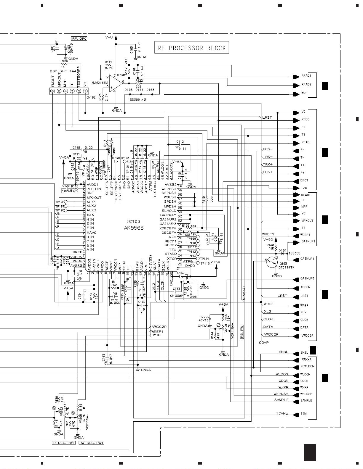
AK8563 (SERVO DIGITAL ASSY : IC103)
• RF Processor IC
Pin Assignment (Top view)
•
AVSS160NC(VSS)59WRF58OSTCC57SLLPFN56SLLPFP55TESTEQRFP
AVDD1 61
RECDIN 62
RRF 63
MPXOUT 64
AUX1 65
AUX2 66
AUX3 67
GIN 68
HIN 69
EIN 70
FIN 71
HAVC 72
DIN 73
CIN 74
BIN 75
AIN 76
RREF 77
VRDCN 78
VRDC 79
AVSS3 80 DVDD21
54
53
TESTEQRFN
PHO52BHO51AGND250AGC3C49AGC2C48AGC1C47ATFM46TESTAGC
45
AGCON44WLDON43XRST42AVDD2
41
AVSS240
WFPDSH39
RFPDSH38
WBLSH37
SPDSH36
MPDSH35
SLHOLD34
GAINUP133
GAINUP232
GAINUP331
XDECEFM30
DECEFM29
RZC28
RECD127
RECD226
TZC25
XTAND24
XTOR23
ATFG22
60
1
AVDD3
2
FPDIN
3
FVREF
4
FPDO
5
WREF
6
VWDC
7
8
VWDCN
9TE10FE11
MPP
TEIN
12
13
BIAS
14
VREF
AGND1
15
16
NC(VSS)
17
XLAT
18
SCLK
SDATA
19
MCLK
20
DVSS
Page 61

Block Diagram
•
CDR-850
HAVC
MPDSH
AIN
BIN
CIN
DIN
SPDSH
EIN
FIN
GIN
HIN
WBLSH
GAINUP1
WRF
58
72
35
76
75
74
73
36
70
71
68
69
37
33
SH
MATRIX
SRFO
SPPO
SADBC
RFOM
SLHOLD56SLLPFN55SLLPFP62RECDIN
DECEFM
XDECEFM63RRF28RZC27RECD126RECD257OSTCC53TESTEQRFN
34
29
30
RFO
FEO
MPP
ADO
BCO
WRF
RF_EQUALIZER
TESTEQRF
RRF
TESTEQRFP11FE10TE
MPP
54
8
FOCUS &
TRACK
ATIP
RRF
FE
TE
ATFM
VRDC
VWDC
P/H & B/H
MPX
TEIN
9
25
TZC
24
XTAND
23
XTOR
44
AGCON
32
GAINUP2
31
GAINUP3
46
ATFM
22
ATFG
47
AGC1C
48
AGC2C
49
AGC3C
52
PH0
51
BH0
65
AUX1
66
AUX2
67
AUX3
64
MPXOUT
WLDON
RFPDSH
WFPDSH
FPDO
FPDIN
FVREF
80
1
AVDD3
VREF
20
21
DVDD
AVSS3
15
DVSS
NC(VSS)
59
NC(VSS)
17
SDATA
18
REGVREF
16
42
SCLK
XLAT
XRST
43
38
39
4
2
3
78
79
VRDCN
APC
77
RREF
VRDC
7
6
VWDC
VWDCN
5
WREF
14
VREF
13
12
BIAS
AGND150AGND2
61
19
45
MCLK
TESTAGC
41
60
AVSS1
AVDD1
40
AVSS2
AVDD2
61
Page 62

CDR-850
Pin Function
•
.oNemaNniPO/InoitcnuF.oNemaNniPO/InoitcnuF
13DDVAI nipylppusrewopevitisopgolanA142DDVAI nipylppusrewopevitisopgolanA
2NIDPFI nipnoitcennocedoidrotinomresaL24TSRXI retsigerehtezilaitinI:"L"teserretsigeR
3FERVFI CPAroftupniegatlovecnerefeR34NODLWI
40DPFO/I
5FERWI CPAetirWroftupniegatlovgnittesrewoP54CGATSETOniptseT
6CDWVO etirWroftuptuolortnocrevirdresaL64MFTAO tuptuolangiselbboW
7NCDWVI etirWrof)–(.pmalortnocrevirdresaL74C1CGAO
8PPMO tuptuolangisllup-hsupniaM84C2CGAO
9NIETI ssecorplangisgnikcartroftupnI94C3CGAO
01ETO tuptuolangisrorregnikcarT052DNGAO egatlovecnereferlanretnirofnipgnilpuoceD
11EFO tuptuolangisrorresucoF150HBO langisFRRfotuptuolevel-mottoB
21SAIBO k7.4=SAIBR.rotsisersaibatcennoC Ω 250HPO langisFRRfotuptuolevel-kaeP
311DNGAO egatlovecnereferlanretnirofnipgnilpuoceD35NFRQETSETOniptseT
41FERVO/I
51)SSV(CN − SSVottcennoC55PFPLLSI ecilsotuarof)+(tupniFPL
61TALXI gnittesretsigerroftupnihctaL65NFPLLSI ecilsotuarof)–(tupniFPL
71ATADSI gnittesretsigerroftupniataD75CCTSOO
81KLCSI gnittesretsigerroftupnikcolC85FRWO tuptuolangisFRetirW
91KLCMI )zHM4475.43(tupnikcolcniaM95)SSV(CN − SSVottcennoC
02SSVDI nipdnuorglatigiD061SSVAO nipdnuorggolanA
12DDVDI nipylppusrewopevitisoplatigiD161DDVAI nipylppusrewopevitisopgolanA
22GFTAO
32ROTXO tuptuonoitcetededutilpmagnikcarT36FRRO tuptuolangisFRdaeR
42DNATXO tuptuonoitcetedrorregnikcarT46TUOXPMO rotinomlangisroftuptuorexelpitluM
52CZTO tuptuolangisnoitcetedssorc-orezgnikcarT561XUAI rotinomlangisrof)1(tupniyrailixuA
622DCERO
721DCERO
82CZRO tuptuolangisnoitcetedssorc-orezFR86NIGI tupni)G(langismaebediS
92MFECEDO )noisrevni(decilsretfatuptuoMFE96NIHI tupni)H(langismaebediS
03MFECEDXO )esahp-evitisop(decilsretfatuptuoMFE07NIEI tupni)E(langismaebediS
133PUNIAGI
232PUNIAGI 27CVAHI slangismaebedisdnaniamfotupniegatlovretneC
331PUNIAGI 37NIDI tupni)D(langismaebniaM
43DLOHLSI dloH:"H"tupnilangisdlohlevelecilS47NICI tupni)C(langismaebniaM
53HSDPMI
63HSDPSI
73HSLBWI
83HSDPFRI
93HSDPFWI
042SSVAI nipdnuorggolanA083SSVAI nipdnuorggolanA
)noisrevnoc
tupniegatlovrotinomresaL
tupniegatlovecnerefeR
2langisnoitcetedkcolbgnidroceR
1langisnoitcetedkcolbgnidroceR
tupnilortnocgnihctiwsBd81+dna0
Bd0:"L",Bd81+:"H"
maeb-niamroftupnieslupelpmaS
dloH:"L",elpmaS:"H"
maeb-edisroftupnieslupelpmaS
dloH:"L",elpmaS:"H"
dloH:"L",elpmaS:"H"
CPAdaeRroftupnieslupelpmaS
dloH:"L",elpmaS:"H"
CPAetirWroftupnieslupelpmaS
dloH:"L",elpmaS:"H"
V/Irofrotsiseratcennoc(tuptuorotinomresaL
/))2nip(NIDPFdnanipsihtneewtebnoisrevnoc
44NOCGAI
/egatlovecnereferlanretnirofnipgnilpuoceD
kcolbgnidrocernU:"L",kcolbgnidroceR:"H"
kcolbgnidrocernU:"L",kcolbgnidroceR:"H"
langiselbboWroftupnieslupelpmaS
45PFRQETSETOniptseT
atadyranibehtretfalangiselbboW(tuptuoGFPITA
26NIDCERI noitcetedkcolbgnidrocerroftupniFR
662XUAI rotinomlangisrof)2(tupniyrailixuA
763XUAI rotinomlangisrof)3(tupniyrailixuA
17NIFI tupni)F(langismaebediS
57NIBI tupni)B(langismaebniaM
67NIAI tupni)A(langismaebniaM
77FERRI CPAdaeRroftupniegatlovgnittesrewoP
87NCDRVI daeRrof)–(.pmalortnocrevirdresaL
97CDRVO daeRroftuptuolortnocrevirdresaL
tupnilortnocDLetirW
NODL:"H",orezoteulav-tesCPAetirWteS:"L"
tupnielbaneCGAelbboW
teserCGA:"L",NOCGA:"H"
esnopserCGArofnipnoitcennocroticapaclanretxE
gnittesdeeps
rezilauqefognittescfrofnipnoitcennocroticapaC
rellecnac-tesffotuptuo
62
Page 63

BA7082F (SERVO DIGITAL ASSY : IC302)
• VCO IC
Block Diagram
•
IN1
16
IN2
15
VO
14
VCTL
13
CT1
12
CT2
11
VCC
10
CDR-850
F
ADJ
9
VCO
SW
Pin Function
•
1
SW1
2
SW2
3
SW3
BW
4
5
BWB
6
1/2FB
7
FOUT
.oNemaNniPO/InoitcnuF.oNemaNniPO/InoitcnuF
11WS
22WS01CCV
33WS112TC
O
tnemtsujda
4WB
5BWB31LTCVI
I
tnemtsujda
tuptuoneporotcelloC
ytilibisneslortnocroftuptuokcolbcigoL
ytilibisneslortnocroftupnikcolbcigoL
9JDAF
211TC
−
−
−
nipCCV
ytilibisneslortnocroftupnikcolbcigoL
6BF2/1I
reilpitlumedycneuqerf2/1dnatnemtsujda
ycneuqerf2/1:L,hguorht:Hhctiws
410VO tnemtsujdaytilibisnesroftuptuo.pmA
tuptuoreilpitlumed
7TUOFO niptuptuoOCV512NI
8DNG
−
nipDNG611NI
I
1/2
8
GND
niptsujdA0f
noitallicsoOCVrofnipnoitcennocroticapaC
-trohsrofesu,yllamroNniplortnocOCV
.)41nip(OVhtiwtiucric
tnemtsujdaytilibisnesroftupni.pmA
tupnignitrevnI:2NItupniesahp-evitisop:1NI
AD1893JST (SERVO DIGITAL ASSY : IC311)
• Sample Rate Converter IC
Block Diagram
•
NC43DATA_I42XTAL_I41NC40XTAL_O39NC38SETSLW
44
1
NC
BCLK_I
WCLK_I
LR_I
NC
VDO
GND
NC
BKPOL_I
MODE0_I
NC
2
3
4
5
6
7
8
9
10
11
12
NC
SERIAL IN
FIFO COEF ROM
13
14
15NC16
RESET
MODE1_I
SERIAL OUT
ACCUM
MULT
CLOCK
TRACKING
17NC18
GND
37NC36
19NC20
MUTE_I
PWRDWN
BCLK_O34NC
35
21
22
NC
MUTE_O
MODE1_O
33
NC
32
WCLK_O
31
LR_O
30
DATA_O
29
NC
28
VDO
27
GND
26
NC
25
BKPOL_O
24
MODE0_O
23
NC
63
Page 64

CDR-850
BA5912AFP-Y (SERVO DIGITAL ASSY : IC351)
• Driver IC
Block Diagram
•
IN1'24IN123OP2-OUT22OP2-IN–21OP2-IN+20BIAS
25
10kΩ
10kΩ
LEVEL
SHIFT
Vref1 Vref1 Vref2 Vref2
REF1
1
MUTE
GND
SWITCH
CH1
2
MUTE1
10kΩ
10kΩ 10kΩ
3
4
5
6
REF1
OUT1–
Pow Vcc1
T.S.D.
10kΩ 10kΩ
10kΩ 10kΩ
7
OUT1+
GND18OP1-IN+17OP1-IN–16OP1-OUT15IN214IN2'
19
LEVEL
SHIFT
SWITCH
11
Pre Vcc
Pow Vcc2
GND
8
OUT2+
10kΩ
9
OUT2–
10
REF2
12
10kΩ
10kΩ
CH2
MUTE
REF2
13
MUTE2
Pin Function
•
.oNemaNniPnoitcnuF.oNemaNniPnoitcnuF
1DNGDNGthgiarts-buS41'2NItnemtsujdaniagrofniptupni2HC
21ETUMnipetum1HC512NItupnidexifniag2HC
31FERnipgnihctiwsferV1HC61TUO-1POtuptuo1.pmaPO
41ccVwoP)1HC(ccVwoP71–NI-1POtupni–1.pmaPO
5–1TUOtuptuoevitagen1HC81+NI-1POtupni+1.pmaPO
6+1TUOtuptuoevitisop1HC91DNGDNGthgiarts-buS
7DNGDNGthgiarts-buS02SAIBtupnisaiB
8+2TUOtuptuoevitisop2HC12+NI-2POtupni+2.pmaPO
9–2TUOtuptuoevitagen2HC22–NI-2POtupni–2.pmaPO
012ccVwoP)2HC(ccVwoP32TUO-2POtuptuo2.pmaPO
11ccVerPccVerP421NItupnidexifniag1HC
212FERnipgnihctiwsferV2HC52'1NItnemtsujdaniagrofniptupni1HC
312ETUMnipetum2HC
64
Page 65

BA5932FP (SERVO DIGITAL ASSY : IC352)
• Driver IC
Block Diagram
•
CDR-850
VREF27OPIN21+26FWD225REV224OPIN21–23OPOUT2122OPIN22
28
4
REV1
10kΩ
10kΩ
10kΩ
10kΩ
5
OPIN11–
6
OPOUT11
7
OPIN12–
10kΩ 10kΩ
2
OPIN11+
10kΩ 10kΩ
3
FWD1
Driver⋅Mute
1
MUTE
Pin Function
•
.oNemaNniPnoitcnuF.oNemaNniPnoitcnuF
1ETUMnipetuM51ccVDLnoitcesegdirbHtuptuodnagnidaolrofccV
2+11NIPOtupnignitrevni-non.pmaPO61+TUODLtuptuoevitisopgnidaoL
31DWFtupnidrawroF71DWFtupnidrawrofgnidaoL
41VERtupniesreveR81+2TUOtuptuorevirD
5–11NIPOtupnignitrevni.pmaPO91–2TUOtuptuorevirD
611TUOPOtuptuo.pmaPO0222TUOPOtuptuo.pmaPO
7–21NIPOtupnignitrevni.pmaPO12ccVnoitceserpgnidaoldnarevirdsexaowtrofccV
8DNGDNGthgiarts-buS2222NIPOtupnignitrevni.pmaPO
921TUOPOtuptuo.pmaPO3212TUOPOtuptuo.pmaPO
01WStupnihctiwsgolanA42–12NIPOtupnignitrevni.pmaPO
11–1TUOtuptuorevirD522VERtupniesreveR
21+1TUOtuptuorevirD622DWFtupnidrawroF
31VERtupniesrevergnidaoL72+12NIPOtupnignitrevni-non.pmaPO
41–TUODLtuptuoevitagengnidaoL82FERVtuptuoegatlovecnerefeR
VCC20OPOUT2219OUT2–18OUT2+17FWD16LDOUT+15LDVCC
21
Vcc
Vcc
8
GND
× 1
10kΩ
10kΩ
9SW10
OPOUT12
TSO
Analog⋅Switch
× 1
× 1
11
OUT1–
× 1
12
OUT1+
LOADING
Vcc
FWD OUT
LOADING
REV OUT
13
14
REV
LDOUT–
65
Page 66

CDR-850
CXD2585Q (SERVO DIGITAL ASSY : IC353)
• Digital Signal Processor IC
Pin Assignment (Top view)
•
1
DD
FILI
PCO
AV
BIAS
VCTL
V16M
VPCO
53
54
55
56
57
58
59
60
FILO
52
1
SS
AV
CLTV
51
50
ASYI
RFAC
49
ASYO
48
0
0
SS
DD
TE
RFDC
ADIO
AV
IGEN
AV
41
42CE43
44
45
46
47
DVDD2
ASYE
MD2
DOUT
LRCK
PCMD
BCK
EMPH
XTSL
DVSS2
XTAI
XTAO
SOUT
SOCK
XOLT
SQSO
SQCK
SCSY
SBSO
EXCK
61
62
63
64
65
66
67
68
69
70
71
72
73
74
75
76
77
78
79
80
1
2
3
4
5
6
7
8
10
11
12
13
14
15
16
17
18
19
0
DD
DV
XRST
MUTE
XLAT
DATA
CLOK
SENS
SCLK9ATSK
WFCK
XPCK
XUGF
GFS
C2PO
SCOR
C4M
0
SS
DV
WDCK
20
MIRR
COUT
40
39
38
37
36
35
34
33
32
31
30
29
28
27
26
25
24
23
22
21
SE
FE
VC
TES1
TEST
DVSS1
FRDR
FFDR
TRDR
TFDR
SRDR
SFDR
DVDD1
FSTO
SSTP
MDP
LOCK
PWMI
FOK
DFCT
66
Page 67

Block Diagram
•
FSTO
C4M
RFAC
ASYI
ASYO
ASYE
BIAS
CDR-850
XTAI72XTAO60VPCO
XTSL58VCTL
V16M
71
69
59
27
16
50
49
48
62
57
Clock
Generator
Asymmetry
Corrector
XUGF13GFS68EMPH
11
10
EFM
Demodulator
WFCK
Corrector
Error
32k
RAM
WDCK14C2PO65LRCK
17
D/A
Interface
PCMD66BCK
3
67
MUTE
37
36
2
TES1
TEST
XRST
XPCK
FILO
FILI
PCO
CLTV
MDP
LOCK
PWMI
SENS
DATA
XLAT
CLOK
SCOR
SBSO
EXCK
SCSY
SQSO
SQCK
RFDC
CE
TE
SE
FE
VC
IGEN
12
53
54
55
52
25
24
23
7
4
5
6
15
79
80
78
76
77
Digital
PLL
Digital
CLV
CPU
Interface
Sub Code
Processor
Servo
Auto
Sequencer
Digital
OUT
SIGNAL PROCESSING
63
64
MD2
DOUT
BLOCK
SERVO BLOCK
73
SOUT
74
SOCK
75
Servo
Interface
MIRR
43
42
41
40
39
38
46
OP Amp
Analog
Switch
A/D
Converter
DFCT
FOK
SERVO DSP
FOCUS
SERVO
TRACKING
SERVO
SLED
SERVO
PWM GENERATOR
FOCUS PWM
GENERATOR
TRAKING PWM
GENERATOR
SLED PWM
GENERATOR
8
19
26
9
20
21
22
33
34
31
32
29
30
XOLT
SCLK
COUT
SSTP
ATSK
MIRR
DFCT
FOK
FFDR
FRDR
TFDR
TRDR
SFDR
SRDR
44
ADIO
67
Page 68

CDR-850
Pin Function
•
.oNemaNniPO/InoitcnuF.oNemaNniPO/InoitcnuF
1VDDD0 − ylppusrewoplatigiD14ETI tupnirorregnikcarT
2TSRXI "L"nehwteseRtesermetsyS24ECI tupnigolanaovresretneC
3ETUMI "H"nehwetuMtupnietuM34CDFRI tupnilangisFR
4ATADI UPCmorftupniatadlaireS44OIDAO noitcennocnoNniptseT
5TALXI
6KOLCI UPCmorftupnikcolcrefsnartatadlaireS64NEGII reifilpmaPOroftupnitnerructnatsnoC
7SNESO UPCottuptuoSNES74VA
8KLCSI tuodaeratad-lairesSNESroftupnikcolC84OYSAO )DDV="H",SSV="L"(tuptuogniws-llufMFE
9KSTAO/Ikcohs-itnuroftuptuodnatupnI94IYSAI tupniegatlovetarapmocyrtemmysA
01KCFWO tuptuoKCFW05CAFRI tupnilangisMFE
11FGUXO
21KCPXO
31SFGO
41OP2CO
51ROCSO
61M4CO
71KCDWO
SS
81VD
91TUOCO/Ilangistnuocrebmun-kcartfotuptuodnatupnI95M61VO/I
02RRIMO/ItuptuodnatupnilangisrorriM06OCPVO LLPMFEdnab-ediwroftuptuopmupegrahC
12TCFDO/ItuptuodnatupnilangistcefeD16VD
22KOFO/ItuptuodnatupnilangisKOsucoF26EYSAI )NO:H,FFO:L(lortnocFFO/NOtiucricyrtemmysA
32IMWPI rotomeldnipsfotupnilortnoclanretxE362DMI )NO:H,FFO:L(lortnocFFO/NOtuolatigiD
42KCOLO/I
52PDMO rotomeldnipsfotuptuolortnocovreS56KCRLO sF=ftuptuokcolcRLecafretniA/D
62PTSSI tsomrennicsidfotupnilangisnoitceteD66DMCPO
72OTSFO nipLATXfoylpitlumedycneuqerf3/2stuptuO76KCBO tuptuokcolctiBecafretniA/D
82VD
92RDFSO
03RDRSO 07VD
13RDFTO
23RDRTO 27OATXO tuptuotiucricnoitallicsolatsyrC
33RDFFO
43RDRFO 47KCOSO kcolbovresehtnituptuokcolctuodaeratadlaireS
53VD
63TSETI
731SETI 77KCQSI tuodaerOSQSroftupnikcolC
83CVI tupniegatlovretneC87YSCSI ROCSRGfosuonorhcnyserroftupnI
93EFI tupnilangisrorresucoF97OSBSO WotPbuSfotuptuolaireS
04ESI tupnilangisrorredelS08KCXEI tuodaerOSBSroftupnikcolC
0 − DNGlatigiD85LTCVI LLPMFEdnab-ediwroftupniegatlovlortnoc2OCV
DD
1 − ylppusrewoplatigiD86HPMEO
SS
1 − DNGlatigiD57TLOXO kcolbovresehtnituptuohctalatadlaireS
.dnammoc
.detceted
UPCmorftupnihctaL
.egdegnillafehttadehctalsiatadlaireS
ybtuptuoKCFRdna0TNMtuptuoFGUX
.dnammocehtgnihctiws
ehtgnihctiwsybtuptuo1TNMtuptuoKCPX
ybtuptuoFORXdna2TNMtuptuoSFG
.dnammocehtgnihctiws
ybtuptuoPOTGdna3TNMtuptuoOP2C
.dnammocehtgnihctiws
si1Sro0S.cnysedocbusrehtienehw"H"stuptuO
ylpitlumedycneuqerf4/1stuptuOtuptuozHM6332.4
.hctipelbairavdnaedomW-VACehtniM61Vfo
sF2=ftuptuokcolcdroW
hctiwsdnammocybROCSRGstuptuO
nipsiht,"H"siSFGnehw;zH064tadelpmassiSFG
,selpmasevitucesnocthgie"L"siSFGfI."H"stuptuo
."1"=NIKLnehwtupnI."L"stuptuonipsiht
tuptuoevirddelS
tuptuoevirdgnikcarT
tuptuoevirdsucoF
DNGyllamron:nipTSET
Notes)
• PCMD is an MSB first. two's complement output.
• GTOP is used to monitor the frame sync protection status. (High:sync protection window released)
• XUGF is the negative pulse for the frame sync derived from the EFM signal. It is the signal before sync protection.
• XPCK is the inverse of the EFM PLL clock. The PLL is designed so that the falling edge of XPCK and the EFM signal transition point coincide.
• GFS goes high when the frame sync and the insertion protection timing match.
• RFCK is derived with the crystal accuracy. This signal has a cycle of 136µs.
• C2PO represents the data error status.
• XROF is generated when the 32K RAM exceeds the ±28 Frame jitter margin.
68
SS
0 − DNGgolanA
54VA
DD
0 − ylppusrewopgolanA
SS
1 − DNGgolanA
15VA
25VTLCI esaercnilaudargroftupniegatlovlortnoc1OCV
35OLIFO )LLPlatigid=evalS(LLPretsamroftuptuoretliF
45ILIFI LLPretsamroftupniretliF
55OCPO LLPretsamroftuptuopmupegrahC
DD
65VA
75SAIBI tiucricyrtemmysafotupnitnerructnatsnoC
46TUODO tuptuotuolatigiD
96LSTXI
17IATXI
37TUOSO kcolbovresehtnituptuoatadlaireS
67OSQSO
1 − ylppusrewopgolanA
DD
2 − ylppusrewoplatigiD
SS
2 − DNGlatigiD
hctiws
)tsrif
LLPMFEdnab-ediwroftuptuonoitallicso2OCV
dnammocybLLP-MFEdnab-ediwroftupnikcolC
BSM,PMOCs'2(tuptuoatadlaireSecafretniA/D
,sisahpmesahcsidkcabyalpehtnehw"H"stuptuO
.sisahpmeonsierehtnehw"L"dna
tupninoitceleslat'X
H:zHM8868.33,L:zHM4439.61
tupnitiucricnoitallicsolatsyrC
.nipsihtaivkcolcretsamlanretxeehttupnI
tuptuoatadleveldnakaepMCP,tib-08QbuS
tuptuoatadTXETDC
Page 69

TK11041M-1 (SERVO DIGITAL ASSY : IC355)
× 1
Temperature
Sensor
VO
3
VCC
1
GND
5
1
V
DD
V
SS
OUT
2
3
• Thermo Sensor IC
Block Diagram
•
CDR-850
S-806E (FUNCTION ASSY : IC702)
• Voltage Detector IC
Block Diagram
•
69
Page 70

CDR-850
PE8001A (AUDIO ASSY : IC401)
• D/A Converter IC
Block Diagram
•
3
BCK
LRCK
DATA
ML/IIS
MC/DM1
MD/DM0
CS/IWO
MODE
MUTE
RST
Serial
1
Input
I/F
2
28
27
26
Mode
23
Control
I/F
24
25
22
Oversampling
SCK
2L
CC
V
20
DAC
8X
Digital Filter
with
Function
Multi-level
Delta-Sigma
Modulator
DAC
Controller
BPZ-Cont
Crystal OSC Power Supply
6
5
4
15
8
14
1
XTI
XTO
CLKO
CC
V
AGND1
AGND2L9V
19
7
DD
V
DGND
2R
OUT
AGND2R
10
Open drain
Low-pass
Filter
Low-pass
Filter
16
18
13
11
21
V
OUT
EXTL
V
OUT
EXTR
ZERO
L
R
Pin Function
•
.oNemaNniPO/InoitcnuF.oNemaNniPO/InoitcnuF
1KCRLI )sf(tupnikcolcKCRL ∗1511CCV − V5+ylppusrewopgolanA
2ATADItupniataD ∗161LTUOVO tuptuoegatlovgolanahcL
3KCBI atadroftupnikcolctiB ∗171CN − noitcennocnoN
4OKLCO kcolcmetsysfotuptuoreffuB81LTXEO nommoc.pmatuptuogolanahcL
5ITXI
tupnikcolc
lanretxeronoitcennocnoitallicsolatsyrC
91L2DNGA − DNGgolanA
6OTXO noitcennocnoitallicsolatsyrC02L2CCV − V5+ylppusrewopgolanA
7DNGD − DNGlatigiD12OREZO galfatadoreZ
8DDV − V5+ylppusrewoplatigiD22TSRIteseR ∗2
9R2CCV − V5+ylppusrewopgolanA32OWI/SCI tcelestamroftupnI/tcelespihC ∗3
01R2DNGA − DNGgolanA42EDOMI
tceleslortnocedoM ∗2
)erawdraH:L,erawtfoS:H(
11RTXEO nommoc.pmatuptuogolanahcR52ETUMI lortnocetuM ∗2
21CN − noitcennocnoN620MD/DMI 1tcelessisahpmeed/atadlortnocedoM ∗2
31RTUOVO tuptuoegatlovgolanahcR721MD/CMI 2tcelessisahpmeed/KCBlortnocedoM ∗2
411DNGA − DNGgolanA82SII/LMI tcelestamroftupnI/hctallortnocedoM ∗2
:etoN
∗ tupnireggirtttimhcS:1
∗ rotsiserpu-lluphtiwtupnireggirtttimhcS:2
∗ rotsisernwod-lluphtiwtupnireggirtttimhcS:3
70
Page 71

PE5056A (FUNCTION ASSY : IC701) • Mode Control Microcomputer
Pin Function
•
.oNtroPemaNniPO/ItnInoitcnuF.oNtroPemaNniPO/ItnInoitcnuF
16PIF6DILGOL 5tuptuodirgLF1423PKCAMOH
25PIF5DILGOL 6tuptuodirgLF2413PQERLOH )ELBANE:L(58598CLroflangisEC
34PIF4DILGOL 7tuptuodirgLF3403PKCOLNUI noitcetedkcolnulatigiD
43PIF3DILGOL 8tuptuodirgLF443PTNITNI_TORI
52PIF2DILGOL 9tuptuodirgLF542PTNILIAFPXI
61PIF1DILGOL 01tuptuodirgLF641PTNIQERMI
70PIF0DILGOL 11tuptuodirgLF740PTNINIMERI )tpurretnI(tupnilortnocetomeR
8DDVO DDVotdetcennoC84CIPPVI DNGotdetcennoC
90KCSKCSROH
010OSOSROL
110ISISRI
2142PLATXOL
3132POCVEXOL )H:DC(FFO/NOOCVredocnE35721P4NACSOL 4tuptuoxirtamyeK
411KCSKCSFO/IH kcolclairesISL,rellortnocmsinahceM45621P3NACSOL 3tuptuoxirtamyeK
511OSOSFOL tuptuolairesISL,rellortnocmsinahceM55521P2NACSOL 2tuptuoxirtamyeK
611ISISFI tupnilairesISL,rellortnocmsinahceM65421P1NACSOL 1tuptuoxirtamyeK
71TESERTESERXIµ )TESER:L(tupniTESER-moc75321P0NACSOL 0tuptuoxirtamyeK
8147PATADLOL
9137PKCOLCLOL
02SSVADNGI DNGotdetcennoC06021P1NIYEKI 1tupnixirtamyeK
1271PESUFXOH
2261PKCLOL
3251POCVXOH
4241PRHT_SFOH
5231PTALCADOH
6221PTSRXOL
7211PTPOXOL )L(tupnilatigidlacitpodetceles76111P8GESOL 8tuptuotnemgesLF
8201PMIRPI
92DDVADDVDDVotdetcennoC96701P6GESOL 6tuptuotnemgesLF
03FERVADDVDDVotdetcennoC07601P5GESOL 5tuptuotnemgesLF
1340PID_TORI
232TXOdesutoN27501P4GESOL 4tuptuotnemgesLF
33SSVDNGDNGotdetcennoC37401P3GESOL 3tuptuotnemgesLF
431XI zHM91.4:noitallicsometsyS47301P2GESOL 2tuptuotnemgesLF
532XO zHM91.4:noitallicsometsyS57201P1GESOL 1tuptuotnemgesLF
6373P1WSIL
7363POLdesutoN77001P01DILGOL 01tuptuodirgLF
8353P4TORI
9343POLdesutoN978PIF8DILGOL 8tuptuodirgLF
0433PQERROL
noitacinummoc
noitacinummoc
noitacinummoc
revird
revird
)L(desuyitnerruc
revird
))detallicso
retrevnoc
)tupniD/A(tupni
hctiwsredocne
)IHRLXdetceles
noitacinummoc
ecivedtnemtaertrofkcolclaireS
ecivedtnemtaertroftuptuolaireS
ecivedtnemtaertroftupnilaireS
)H:retrevnocSFonsiereht
noitacinummoclaires58598CL
LLP(L:retrevnocSFonsiereht
latigidzHk1.44(tuptuohguorhtSF
)L:NOhguorhtSFnehwtupni
)TESER:L(redrocedPITArof
yratorfotupninoitcnitsidnoitceriD
)edomnoitartsnomedon:
ecivedtnemtaertroftuptuoEC
9427P3LESII
0517P2LESII
1507P1LESII
nehwlatigiddetceles(FFO/NOLATX
25DDVDDVDDVotdetcennoC
DELroftuptuoatadnoitacinummoC
85221P3NIYEKI 3tupnixirtamyeK
DELroftuptuokcolcnoitacinummoC
95121P2NIYEKI 2tupnixirtamyeK
16711P0NIYEKI 0tupnixirtamyeK
DELroftuptuohctarnoitacinummoC
26611P5TORI
nehwlatigiddetceles(FFO/NOLLP
36511P6TORI
46411PGES_LNIFOL )H:nothgiL(tuptuoges-EZILANIF
A/DroftuptuohctalnoitacinummoC
56311P01GESOL 01tuptuotnemgesLF
tuptuoTESER,rellortnocmsinahceM
66211P9GESOL 9tuptuotnemgesLF
hctiwsyeK,lortnocetomeR,lellaraP
86011P7GESOL 7tuptuotnemgesLF
17DAOLV
Hdexif(FFO/NOedomnoitartsnomeD
67101P0GESOL 0tuptuotnemgesLF
:H(4tupnihctiwsRETCELESTUPNI
879PIF9DILGOL 9tuptuodirgLF
087PIF7DILGOL 7tuptuodirgLF
CDR-850
rofesnopsernoitacinummoC
:HmorfL(rellortnocmsinahcem
:LmorfH()noissimrepnoitacinummoC
)dnenoitacinummoC
redocneyratorfonoitcetednoitarepO
)tpurretnI(hctiws
REWOP:L(noitcetedNWODREWOP
)NWOD
noitacinummocrellortnocmsinahceM
)tpurretnI(tseuqer
:H(3tupnihctiwsRETCELESTUPN
)LAIXAOCdetceles
:H(2tupnihctiwsRETCELESTUPN
)LACITPOdetceles
:H(1tupnihctiwsRETCELESTUPN
)UBE/SEAdetceles
:H(5tupnihctiwsRETCELESTUPNI
)OLRLXdetceles
:H(6tupnihctiwsRETCELESTUPNI
)ENILdetceles
71
Page 72

CDR-850
PE5073A (SERVO DIGITAL ASSY : IC204) • MECHANISM Control Microcomputer
Pin Function
•
.oNkraMemaNO/ItnInoitcnuF.oNkraMemaNO/ItnInoitcnuF
1/0KCS/23PKCSM)I(OH
2/0KCS/33POSM)I(OH
30OT/43POLdesutoN340DA/04P0DAO-
41OT/53P0NCTSOL
52OT/63PKOFI- )"H":KOsucoF(KOsucoffotupnI540ssVDNG-- tropfoDNG
63OT/73PTSRLOL
7TESERTESERXI- "L":teserfotupnI740MWP/01PPSPSI-
81ddVV5+-- tropnahtrehtoseilppusrewopevitisoP841MWP/11PIAGDIL
92XKCOLCI-
011XKCOLC-111ssVDNG-- tropnahtrehtoDNG15/2OS/41P2OSIH tuptuoatadlaireS
2100PECEXOH
3110PECEROL "H":NOrewopdroceredoidresaL3561PMC8DOL H:csidR-DCmc8
4120PCNOLdesutoN4571PCNOLdesutoN
5130PCNOLdesutoN550ddVV5+O tropfoseilppusrewopevitisoP
6140PLES5TIOH
7150PCSXEXOH
8160PCNYSAXOH "L":knisemarfPITA852INA/27PBFR)A(I9170PECNEX)I(OH "H":tuptuoelbanelaires58598CL953INA/37PPMET)A(I- )tupniD/A(rosneserutarepmeT
02/76PVLCOH edomVAC/VLCovreseldnipS064INA/47PCPOFR)A(I-
12/66PVLCEOH edomVLCelbboW/MFEovreseldnipS165INA/57P2CDWV)A(I-
22RW/56PRWXOL
32DR/46PDRXOL
4291A/36PTLXOH
5281A/26PKCSSOH
6271A/16POSSOH
7261A/05PTALAOH
8251A/75PKLCSOH
9241A/65PP2_PTOL
0331A/55PP1_PTOL 073ferVADNG-1321A/45P4WPDLOL
2311A/35P3WPDLOL 270PTNI/12PGFI- noitcetedGFeldnipS
3301A/25P2WPDLOL 371PTNI/22PPITAI- noitcetedcnysPITA
439A/15P1WPDLOL 47/2PTNI/32PROCSI- noitcetedcnysemarf5852DXC
538A/05P0WPDLOL 573PTNI/42PCNYSBUSI- noitcetedcnysemarf58598CL
637DA/74P7DAO-
736DA/64P6DAO- 775PTNI/62PNI5TII-
835DA/54P5DAO- 870IS/72PISMI-
934DA/44P4DAO- 971IS/032PKCAMI-
043DA/34P3DAO- 081O0S/13PESUFXI-
epytsuonorhcnys
epytsuonorhcnys
)03+yaled
"L":CImetsyslatigid
noitallicsokcolc
"L":gnidaer
)PCOT="L",SNES="H"(
"H":tuptuoelbane
dnammoc
dnammoc3658KA
dnammoc3658KA
dnammoc
tuOdaeRlaireS
troptuptuotseT
enilsserddaataD
72
kcolcfotuptuokcolcrefsnartlaireS
kcolcfotuptuoatadrefsnartlaireS
T3(tnemtsujdaygetartsroftuptuO
dnametsysovresroftuptuoteseR
ehtnehw1XlanimretehtotstupnI
edistuoehtmorfdeilppussikcolc
hctiwstupnilanimret5PTNI
noitazinorhcnyslanretxe58598CL
gnidaerroftuptuolangisebortS
yromemlanretxefonoitarepo
gnitirwroftuptuolangisebortS
yromemlanretxefonoitarepo
Q5852DXCrofylnotuptuohctaL
3658KArofylnotuptuohctaL
Q5852DXCroftuptuokcolclaireS
142DA/24P2DAO-
241DA/14P1DAO-
44/BTSABTSAO-
64tsetDNG-- 0ssVottcennoC
metsysroflanimretnoitcennoclatsyrC
94/2KCS/21PKCQSIH
05/2IS/31PISQSI-
ecivedtnemtaerttsetroftuptuoelbanE
2551PCERMH
650INA/07PPPET)A(I-
751INA/17PTFR)A(I-
266INA/67PYART)A(I-
367INA/77P7DA)A(I- )tupniD/A(desutoN
46ddVAV5+-- retrevnocD/ArofylppusrewopevitisoP
dnaQ5852DXCroftuptuokcolclaireS
561ferVAV5+--
dnaQ5852DXCroftuptuoatadlaireS
66ssVADNG-- retrevnocD/ArofDNG
760ONAFERW)A(I- )tuptuoA/D(1rewopdroceR
861ONAR2CDWV)A(I- )tuptuoA/D(2rewopdroceR
962ferVAV5+--
170PTNI/02PLIAFPXI- noitcetederuliafrewoP
rewopresaldrocerfognittestuptuO
67/4PTNI/52PTDFRXI- L:detcetedsiFRkcabyarpMFE
enilsserddaataD
sseccayromem
VAC
L:retuoniR-DCmc21
H:retuoni
Q-bus
Q-bus
"H":rellortnoc
)tupniD/A(FR
)tupniD/A(FR
)tupni
)tupni
)PMALC/NEPO(
retrevnoc
retrevnoc
retrevnoc
epytsuonorhcnys
"L":rellortnoc
langissserddanoitisopetanidrobuS
lanretxeroflangishctallanretxedna
eldnipstatuptuoMWPevirdeldnipS
,DCfosetunim81rofCER,YALP
R-DCmc8fosetunim9rofCER,YALP
Q5852DXCrofylnotuptuokcolclaireS
Q5852DXCrofylnotupniatadlaireS
edomottuptuoekahsdnahlaireS
rof(rorregnikcartfokaepotkaeP
)tnemtsujdaniaggnikcart
kcabyalpfoepolevneedisreppuehT
kcabyalpfoepolevneedisrewolehT
D/A(CPOgninnurrof1thgilnruteR
D/A(CPOgninnurrof2thgilnruteR
)tupniD/A(noitisopgnidaoL
D/ArofnoisserpmiegatlovdradnatS
D/Arof2noisserpmiegatlovdradnatS
D/Arof3noisserpmiegatlovdradnatS
noitisopCOT(rosnesnoitisopCOT
tupnilangisSNESQ5852DXC,))"L"=(
kcolcfotupniatadrefsnartlaireS
edomottupniekahsdnahlaireS
neewtebnoitacinummocnehw"L"
rellorotnocedoMdna5898CL
Page 73

PDJ014A (SERVO DIGITAL ASSY : IC205)
• ATIP DECODER
"External Port"-output from PDJ014A (External RAM area (2C000H to 2C0FFH)
Pin Function
•
.oNkraMemaNO/ItnInoitcnuF
540AOP1PUNIAGOL )"H"=WR-DC(WR-DCrofhctiwsniaG
641AOPCPORDCOL CPOgninnurR-DCroflangiSlortnoctiucricCA
742AOP3PUNIAGOH WR-DCrofrewopsaibfotuptuonoitcerrocerutarepmeT
943AOPOHdesutoN
054AOPSREYHPOL "H":esarElacisyhP
155AOPLESSOL "L"teser,noitcetedepolevnerorregnikcarT
256AOPNOCGAOL noitcartxeelbboWroftiucricCGAfoFFO/NO
357AOPOLdesutoN
450BOPTUOLOL "H"nepognidaoL
551BOPNILOL "H"esolcgnidaoL
652BOPOLdesutoN
753BOPSCEEOL atadMORPEEgnidaerdnagnitirwroftuptuoelbanE
954BOP4NCTSOL
065BOP3NCTSOL
166BOP2NCTSOL
267BOP1NCTSOL
360COP2GETOH
562COP0GETOH
663COPRX/WROL )"H"=WR-DC(hctiwsrehto/WR-DC
764COPOHdesutoN
965COPDCXOL )"L"=DC(hctiwsrehto/DC
076COPLBNEOL tuptuoFFO/NODL
177COPETUMAXOL )rellortnocedomehtfonoitcurtsniehtgniwollof("L"oiduafoetumspetslaniF
tuptuolortnocygetartS
reifilpmarorregnikcartfotnemtsujdaniaG461COP1GETOH
CDR-850
73
Page 74

CDR-850
7.1.2 DISPLAY
PEL1097 (FUNCTION ASSY : V701)
• FL TUBE
1 35
• Anode & Grid Assignment
74
Page 75

CDR-850
• Pin Assignment
75
Page 76

CDR-850
7.2 BLOCK DIAGRAM
A–D RFDC
RF AMP CIRCUIT
IC102, IC101
IC316
PDK033A
SERVO AMP
HF
Disc (CD, CD-R, CDRW)
PICUP ASSY
KRS-200A
FG
SPDL MOTOR
SLD MOTOR
LOADING
MOTOR
A–H
LD CONTROL
CIRCUIT
IC351
BA5912AFP-Y
SLD DRIVER
SPDL DRIVER
66–71
73–76
IC103
AK8563
RFPROCESSOR
RUNNING OPC
CIRCUIT BLOCK
TE
HF
RFWBL
IC247
PA9004A
SERVO AMP
RFOPC
AOUT
RFDC
FE
TE
RFAC
IC353
CXD2585
CD DECODER
IC205
PDJ014A
ATP DECODER IC
76
IC352
BA5932FP
FCS DRIVER
TRK DRIVER
LOADING DRIVER
IC705
BR93LC46AF
EEPROM
FL DISPLAY
PEL1097
IC701
PD4968A
MODE CONTROL
MICROCOMPUTER
KEY MATRIX
Page 77

CDR-850
34.5744MHz
14.2872MHz
REC VR
IC309
BA7082
VCO IC
PIN INPUT
Lch Rch
IC801
AK5340-VS
AD CONVERTER
ADLRCK
ADBCK
ADDATA
LH64256CK-70
IC301
D-RAM
XLR-3 INPUT
Lch Rch
DA CONVERTER
Parallel
Remote
IC401
PE8001A
DALRCK
DABCK
DADATA
16.9344MHz
IC405
IC405
IC406
Lch
XLR-3
OUTPUT
Rch
Lch
PIN
OUTPUT
Rch
HP OUTPUT
RFAC
RFAC
PD4956A
MECH. CONTROL
MICROCOMPUTER
CDLRCK, CDBCK
CDDATA, CDTX
RFOPC(60pin)
AOUT(61pin)
IC204
IC308
LC89585
EFM ENCODER IC
DIRBCK
DIRLRCK
DIRDATA
IC318
74HC4053
SW
DIRBCK
DIRLRCK
DIRDATA
IC311
AD1893JST
Fs CONVERTER
MODE DISPLAY LED
D707, D708
16.9344MHz
IC309
PCX1021
VCO IC
WAVEFORM
SHAPING CIRCUIT
IC3001
SN75157P
Digital in
AES/EBU
Digital in
COAXIAL
Digital in
OPTICAL
Digital out
COAXIAL
Digital out
OPTICAL
IC704
BU2092F
LED DRIVER IC
77
Page 78

CDR-850
7.3 DIAGNOSIS
7.3.1 Diagnosis method when INPUT ASSY is removed.
This product operates even if there is no INPUT ASSY when the terminal of the figure below is shorted.
J
FUNCTION ASSY
SIDE B
SHORT
J708 - 5PIN(REMOTE)
J708 - 1PIN(GND)
78
Page 79

CDR-850
7.3.2 Laser Hour Meter display and Error code display for service.
CDR-850 can be displayed the total of the lighting time of Laser diode and the error code for service.
When this product keeps pushing the STOP key in the TEST mode (potitioin of INPUT selector AES/EBU in ST0P) for about five seconds, the
following displays are done by FL display.
**** **
Laser Hour Meter display Error code Number
Four digit in the left of FL : Total lighting time of laser diode.
Two digit in the right of FL : Error code for service.
0-5100 hours are displayed at the total lighting time of laser diode.
As for the error code for service, Error Number displayed as "CHECK DISC" or "CHECK" is displayed.
Refer to the attached table to the content.
As for the initialization of the total lighting time of laser diode, when you keeps pushing the MENU key and the SKIP SET key at the same time
for five seconds when this product is STOP at the AES/EBU position of the INPUT selector in the TEST mode is initialized.
"CLEAR" is displayed in FL display, and the total time is cleared.
Initialization of error code display.
When the power is turned on again, the error code is automatically cleared.
• Service Codes and Countermeasures
edoCstnetnoCtluaFfonoitacoLesuaCtniopkcehC
0H
1H
2H
5H
*L
*E
*P
.esolc/nepo
etarepotonseodtinU
sidrocehtnehwneve
.teltuootnidetresni
)deyalpsidKCEHC(
.tiucricni
snoitaraperpgnidroceR
.nepotonseod
dna,detseuqersi
erasnoitarepo
.degdelwonkca
yart,demrofrepebtonnac
.elbissopmignidroceR
)deyalpsidKCEHC(
yartgnirudspotstinU
)deyalpsidKCEHC(
)deyalpsidKCEHC(
sicsidnehwspotstinU
gnidaertuohtiwdetresni
.noitamrofnilanretnieht
507CI.tluaf507CI•
csidnehwpotssnoitarepO
tratskcabyalp,detresnisi
ESUAP/CER,detseuqersi
.noitisopdetangised
.detresni
)deyalpsidCSIDKCEHC(
.csidmorf
.rellortnocedom,rellortnoc
.rorreegatlovtupninip
otdevomebtondluocpukciP•
msinahcemniGNsinoitacinummoC:0H
truafdetcetedrellortnocmsinahceM:1H
42,32,22sniprellortnocmsinahceM:2H
.detcetedneebsahtluafnoitcesgnidaoL
.detcetedneebsahtluafnoitcesredilS
.detcetedneebsahtluafnoitceseldnipS
.detresnineebsahcsidfoediskcaB•
neebsahstsudrosehctarcshtiwcsiD•
.yllamrondetatorebtondluoccsiD•
deniatboebtondluoclangisdetangiseD•
.gniredlosytluaF•
.tiucric-trohsnrettaP•
.tiucric-trohsstraP•
.rewopytluaF•
.rosnesnoitisopyartytluaF•
.rotomgnidaolytluaF•
.tnesbaelbacelbixelF•
.tiucricevirdytluaF•
.WSnoitisopCOTytluaF•
.rotomeldnipsytluaF•
.tiucricevirdeldnipsytluaF•
.noitcetedGFnirorrE•
.tiucricLBWytluaF•
.tiucricredocedytluaF•
.hgihsietarrorrE•
402CI
msinahcem(
)rellortnoc
)600JDP(502CI
302CI
507CI
.tiucric-trohsnrettap,gniredlosytluaF•
.rewopytluaf,tiucric-trohsnrettaP•
106S
.tiucric-trohsnrettap,gniredlosytluaF•
.daerebtonnacsedocbus,PITA•
)375CH47DH(
)4009AP(742CI
)FL64CL39RB(
)2395AB(253CI
)03201UPM(
)2395AB(253CI
)5852DXC(353CI
156CP
)K3085LJN(
)2395AB(253CI
)5852DXC(353CI
79
Page 80

CDR-850
edoCstnetnoCtluaFfonoitacoLesuaCtniopkcehC
*C
*F
*A
.snoitarepo
*d
.snoitarepo
.detresni
erofebpotssnoitarepO
.tessiESUAP/CER
)deyalpsidKCEHC(
gnirudpotssnoitarepO
.gnidrocerrokcabyalp
)deyalpsidKCEHC(
deyalpsidsiCSIDKCEHC
gnirudspotstinudna
detalergnidrocer
deyalpsidsiCSIDKCEHC
gnirudspotstinudna
detalergnidrocer
noitamrofnilanretnicsiD
tinudnadaerebtonnac
sicsidnehwspots
.detcetedneeb
.detresni
.lamrontonsinoitcetedFR•
.sucofoN•
.deppots
sahtluafdetalerrewopresalgnidroceR
neebsahstsudrosehctarcshtiwcsiD•
.tuptuotonsirewopgnidrocerreporP•
.detcetedneebsahtluafnoitcespukciP
neebsahstsudrosehctarcshtiwcsiD•
.sucofoneroferehtdnadetresni
.tuptuotonsirewopresalreporP•
.gnidrocergniruddetcetedneebsahpotS
era.cte,stsud,sehctarcscsiD•
sahtinudnasnoitarepognitcurtsbo
.edoidresalytluaF•
.noitcetedFRnirorrE•
.tiucricBFR,TFRytluaF•
.rewopgnidrocertneiciffusnI•
.daerebtonnacsedocbus,PITA•
.edoidresalytluaF•
.tiucricevirdsucofytluaF•
.pukcipytluaF•
eraevobaesohtnahtrehtosedoc
.spotstinuehtdnadetareneg
lanoitareponehwylnodetareneg
.ytluafsirewop
)4009AP(742CI
)3658KA(301CI
.tiucric-trohsnrettap,gniredlosytluaF•
.rewopytluaf,tiucric-trohsnrettaP•
.tiucric-trohsnrettap,gniredlosytluaF•
.rewopytluaf,tiucric-trohsnrettaP•
,derruccoevahsmelborperawdrahfI
,detarenegerasrebmun*ddna*Aerofeb
erasedocecivreseseht,yltneuqesnoC
.csidehtoteudderruccoevahsmelborp
tiucric-trohsnrettap,gniredlosytluaF
rotiucric-trohssahnrettapfielbissoP
)40S7CT(802CI
)41S7CT(902CI
)2395AB(253CI
)5852DXC(353CI
Note) * indicates the mechanism mode and are the following numbers.
No. Mechanism Mode No. Mechanism Mode
0 PLAY 8 Search
1 OPEN 9 REC/PAUSE
2 STOP A REC
3 – B TOC REC
4 – C OPC
5 Setup D TOC check
6 TOC read E PMA, actual pause recording
7–
80
Page 81

7.3.3 About the detailed error code
CDR-850
In CDR-850, when "SKIP PLAY" key and "MENU" key are pushed
at the same time on the ordinary mode, the error code of details is
displayed in FL display. As for the error code of details, the packing
improvement is not done. When the power supply is turned off, the
error code of details is deleted.
The display of eight digits is as follows.
88888888
1234
The value of two digits (eight digits in total) displayed in 1-4 is
displayed as follows.
Two digits displayed in 1 : Operation when figure of digit of
subordinate position does error
detection.
* 0: Uncertainty
* 1: Tray OPEN
* 2: Tray CLOSE or STOP
* 3: SET_UP (disk start-up)
* 4: TOC and PMA lead (SET_UP is included)
* 5: PLAY
* 6: SERCH
* 7: REC/PAUSE
* 8: REC
* 9: Lead OUT REC
* A: TOC REC
* B: PMA REC
* C: Power CALIBRATION
* D: TOC CHECK
* E: ACTUAL PAUSE REC
* F: Uncertainty
09; DIRC use direct sequence forward 1 truck Jump
repeat.
10; DIRC use direct sequence reverse 1 truck Jump
repeat.
11; Auto sequence 10 truck forward jump repeat.
12; Auto sequence 10 truck reverse jump repeat.
13; Auto sequence 50 truck forward jump repeat.
14; Auto sequence 50 truck reverse jump repeat.
15; Auto sequence forward M truck move.
16; Auto sequence reverse M truck move.
17; PAUSE.
18; PLAY.
19; Seek truck 0.
20; Search at blank.
21; REC.
22; REC to PAUSE (REC END).
23; ATIP TIME search.
24; Q code TIME search.
25; Q code truck search.
26; forward 300 truck move.
27; reverse 300 truck move.
30; TOC area search.
31; Tray open.
32; Tray close.
33; Setup (to PLAY).
34; TOC lead.
35; PLAY normal.
36; Search to PLAY.
37; REC PAUSE.
39; Lead out REC.
40; TOC REC (lead Inn).
41; PMA REC.
42; PCA REC.
43; TOC check.
44; ACTUAL REC PAUSE.
45; Initialization.
47; 2Tr JUMP specification at PAUSE.
48; 1Tr JUMP specification at PAUSE.
However, when "F1" is displayed in 2, the NG pin number
of mechanism contoller is displayed in 1.
Two digits displayed in 2 : Error mode.
Mode No. or even 0-79 is an error where mechanism contoller is
generated.
Mode No.; Mode name.
00; Irregular mode (An internal uncertain state, at hard
reset).
01; Invalid mode.
02; STOP.
03; Laser diode turning on (reproduction power).
04; Focus 0N.
05; Spindle ON.
06; Tracking ON.
07; DIRC use direct sequence forward 1 truck jump.
08; DIRC use direct sequence reverse 2 truck jump.
51; Search to PAUSE.
52; PMA lead.
53; Ratings record of Laser diode power output.
54; Searches the area where is Q code.
57; maximum record ofLaser diode power output.
58; Record power of Laser diode continuous sweep
mode.
59; Slider forward move.
60; Slider reverse move.
61; The line speed and the track pitch of the disk are
calculated by T0 and Tl measurement.
62; Auto sequence 1 truck forward jump.
63; Auto sequence 1 truck reverse jump.
64; Auto sequence 1 truck forward jump repeat.
65; Auto sequence 1 truck reverse jump repeat.
66; Auto sequence 10 truck forward jump.
67; Auto sequence 10 truck reverse jump.
68; Scanning mode which uses auto sequence 10 truck
forward jump (It is a sound).
69; Scanning mode which uses auto sequence 10 truck
reverse jump (It is a sound).
81
Page 82

CDR-850
70; Auto sequence 50 truck forward jump.
71; Auto sequence 50 truck reverse jump.
72; High-speed scanning mode which uses auto se-
quence 50 truck forward jump.
73; High-speed scanning mode which uses auto se-
quence 50 truck reverse jump.
74; The number of jumps in forward DTRNUM by com-
bining auto sequence 2N truck jump.
75; The number of jumps in reverse DTRNUM by com-
bining auto sequence 2N truck jump.
76; REC mode continuance processing after power
failure returns.
78; Search at blank.
79; Return mode when "Picup jump" and "Coming off
by focus" are generated in REC.
Error where mechanism contoller is generated.
91; Loading error.
C7; Not REC/PAUSE of Power CALIBRATION though
60 seconds passed.
d0; This product stops for NG or the ST0P key input in
Redum.
d4; Data has not become complete by TOC and PMA
lead.
d7; RF check NG at REC/PAUSE.
db; PMA/REC will not end in 60 seconds.
dd; This product stops for the TOC check error or the
STOP key input.
d f; Not REC/PAUSE in 60 seconds, The REC begin-
ning cannot be done in ten seconds.
The return after Picup jump will not end in 60 sec-
onds.
F0; mechanism contoller communication error.
F1; mechanism contoller hardware error : In this case,
the NG pin number of mechanism contoller is dis-
played in TRACK.
F2; mechanism contoller A/D input (RFT,RFB) error.
F5; Serial Namber error forRID.
Two digits displayed in 3 : Recording sub-mode when error
generation is done.
10: REC/PAUSE is being set.
20: REC/PAUSE is being.
30: REC is being.
40: REC stop is being.
50: Unlock and SCMS is stopping.
Two digits displayed in 4 : Other states when the error generation
is done are displayed by the HEX code.
bit7: Focus coming off.
bit6: Synchronization coming off is detected at REC.
bit5: Picup jump detection at REC.
bit4: TOC lead error (Data does not become complete).
bit3: The A/D value is abnormal of RFT and RFB.
bit2: There is no meaning.
bit1: There is no meaning.
bit0: There is no meaning.
82
Page 83

8. PANEL FACILITIES AND SPECIFICATIONS
• PANEL FACILITIES
FRONT PANEL
COMPACT DISC RECORDER
POWER
MANUAL
ON
OFF
CDR-850
SKIP ID
SET
TRACK NO.
AUTO/
CLEAR SKIP PLAY
WRITE
[MANUAL]
FINALIZE
MENU
ERASE
OPEN/
CLOSE
RECORD
REC
MUTE
MARGIN
TIME/
INPUT SELECTOR
DIGITAL ANALOG
XLR
+4dBu
XLR
COAX
–8dBu
OPT
AES/
EBU
DIGITAL
SYNCHRO
REC LEVEL
LR
5
46
37
LINE
28
19
010
LEVELPHONES
MIN MAX
PROFESSIONAL
CDR-850
The operations available using buttons marked (*) are also
available using the buttons with the same names or
inscriptions on the remote control unit.
1 POWER switch
2 SKIP ID SET, CLEAR buttons
3 SKIP PLAY button
4 COPY-BIT indicator
5 MENU button
6 Function indicator
Recording .............................................. Lights red
Recording mute and writing to (PMA) ... Blinks red
Playback................................................ Lights green
Preparing to erase................................. Blinks orange
Erasing .................................................. Lights orange
7 Disc tray
8 OPEN/CLOSE 0 button
9 RECORD ¶ (record) button*
0 REC MUTE • (record muting) button*
- TIME/MARGIN button*
= INPUT SELECTOR knob
~ DIGITAL SYNCHRO button
! REC LEVEL (recording level) knobs
(outer: Left, inner: Right)
@ PHONES LEVEL (headphone level) control
# PHONES (headphones) jack
$ 7 (stop) button*
% 8 (pause) button*
^ 3 (play) button*
& 4 1, ¡ ¢ (search) buttons*
* Display panel
( ERASE button
) FINALIZE button
_ TRACK NO. WRITE (MANUAL) indicator
+ TRACK NO. WRITE (MANUAL) button*
¡ TRACK NO. AUTO/MANUAL button
83
Page 84

CDR-850
DISPLAY PANEL
1 SYNC
Lights when automatic digital-source synchro recording
is activated.
2 RPT-1
Lights during repeat playback.
3 PGM
Lights in the program mode.
4 #
Lights during playback.
5 FADER
Blinks during fade-in/out.
6 *
Lights or blinks during pause.
7 Track display
Displays the track number.
8 Character display
Displays messages.
9 Time display
Displays the elapsed playing time, remaining playing
time, total playing time, elapsed recording time,
remaining recording time, total recording time and
remaining time until the end of finalization.
0 CD-RW
Blinks during disc identification and lights steadily when
the disc format is recognized.
CD: Lights if the loaded disc is a pre-recorded CD
or finalized CDR.
CDR: Lights if the loaded disc is a CD-R disc that is
not finalized.
CD-RW: Lights if the loaded disc is a CD-RW disc.
- FINALIZE
Lights if the loaded disc is a finalized CD-RW disc60
and.
= REC
Lights during record mode. Blinks in the record muting
mode.
~ AUTO TRACK
Lights when automatic track number write during
recording is activated.
! Signal level indicator
Displays the input level during record or the play level
during playback.
@ SKIP ON
Lights, goes off or blinks during skip ID setting or
clearing.
# Sampling frequency indicator
Displays the sampling frequency (Fs) of the current
digital input. All indicators are turned off when the input
signal is interrupted.
84
Page 85

REMOTE CONTROL UNIT
R-800
CU-PD084
FADER
REPEAT
123
456
789
10 >10
PGM CHECK CLEAR
COMPACT DISC RECORDER
REMOTE CONTROL UNIT
TRACK NO.
WRITE
REC
TIME
CDR-850
Functions of the remote control unit
Operations performed by buttons marked (*) can also be
carried out by using buttons with the same name on the main
unit.
1 FADER button
2 1/¡ (manual search) buttons*
3 REPEAT button
4 7 (stop) button*
5 Numeric buttons 1 to 10, >10
6 PGM (program) button
7 CHECK (program check) button
8 ¶ REC (record) buttons*
To record, press the 2 buttons simultaneously.
9 TRACK NO. WRITE (manual) button*
0 • (record muting) button*
- 4/¢ (track search) buttons*
= 3(play) button*
~ 8 (pause) button*
! TIME button*
@
CLEAR (program clear) button
'
Recordable
85
Page 86

CDR-850
• SPECIFICATIONS
1. GENERAL
Model ....................................... Compact disc audio system
Applicable discs ......................... CDs, CD-Rs and CD-RWs
Power supply
U.S. models ...........................................AC 120 V, 60 Hz
European models ...................AC 220 – 230 V, 50/60 Hz
Power consumption...................................................... 24 W
Operating temperature .................................. +5°C to +35°C
(+41°F to 95° F)
Weight (without package)............................. 7.0 kg (15.4 lb)
Max. dimensions ............... 482 (W) x 393 (D) x 105 (H) mm
19 (W) x 15-1/2 (D) x 4-1/8 (H) in.
2. AUDIO UNIT
Frequency Response ........................ 2 Hz to 20 kHz ± 1 dB
Playback S/N............................................................. 109 dB
Playback Dynamic Range ........................................... 98 dB
Playback T.H.D. ..................................................... 0.0022%
Recording Analog S/N................................................. 92 dB
Recording Analog Dynamic Range .............................93 dB
Recording Analog T.H.D. ......................................... 0.006%
Recording Digital S/N................................................ 108 dB
Recording Digital Dynamic Range .............................. 97 dB
Recording Digital T.H.D. ........................................ 0.0022%
XLR O/P level (0 dBfs: >10 kΩ load) ..................20 ± 1 dBu
RCA O/P level (0 dBfs: >10 kΩ load).................... 8 ± 1 dBu
Wow & Flutter...............................................Un-measurable
(±0.001% W.PEAK)
Number of channels .............................................. 2 (stereo)
All measurements are to EIAJ standards.
3. INPUT CONNECTORS
Analog XLR-3 type (input impedance: 10 kΩ)
Nominal level +4/–8 dBu switchable
Analog RCA Phono type (input impedance: 10 kΩ)
Optical Digital Input (SPDIF)
Coaxial Digital Input (SPDIF - impedance 75 Ω)
AES/EBU Digital Input (balanced - impedance 110 Ω)
Remote Control Connector ................................... 8 pin DIN
4. OUTPUT CONNECTORS
Analog XLR-3 type nominal level +4/–8 dBu (menu select)
Analog RCA Phono type
Optical Digital Output (SPDIF)
Coaxial Digital Output (SPDIF - impedance 75 Ω)
5. ACCESSORIES
÷ Power cord
÷ Remote control unit
÷ 2 x size AAA/R03 dry cell batteries
÷ 2 x audio cables
÷ Operating Instructions
÷ HHB CDR-74 silver disc
÷ HHB Recording Media Guide
÷ HHB Registration Card
6. PICK UP
÷ Laser wavelength (λ) ................................ 778 to 787 nm
÷ Object lens out (3 beam total) ............................... 23mW
÷ Laser class .................................................................IIIb
NOTE:
The specifications and design of this product are subject to
change without notice, due to improvements.
1
2
3
5
Red
White
CU-PD084
REC
TRACK NO.
WRITE
FADER
REPEAT
123
456
789
10 >10
PGM CHECK CLEAR
COMPACT DISC RECORDER
REMOTE CONTROL UNIT
'
Recordable
1Audio cables ... x 2 : PDE1003 (L=1.2m)
(analog recording input, analog playback output)
2AC power cord : DDG1072 (MY TYPE)
(L=1.2m)
: DDG1028 (KU/CA TYPE)
3Remote control unit : PWW1122 (R-800)
4AAA/R03 dry cell batteries ... x 2
5HHB CD-R disc : PEX1007
4
TIME
CDR74
86
Page 87

CDR-850
ORDER NO. RRV2077M T – ZZK FEB. 1999 Printed in Japan
87
Page 88

 Loading...