2010
CDJ-850
For details, refer to "Important Check Points for good servicing".
MULTI PLAYER
CDJ-850
THIS MANUAL IS APPLICABLE TO THE FOLLOWING MODEL(S) AND TYPE(S).
Model Type Power Requirement Remarks
CDJ-850 SYXJ8 AC 220 V to 240 V
CDJ-850 CUXJ AC 120 V
CDJ-850 FLXJ AC 110 V to 240 V
CDJ-850 KXJ5 AC 220 V
CDJ-850 AXJ5 AC 220 V to 240 V
ORDER NO.
RRV4128
PIONEER CORPORATION 1-1, Shin-ogura, Saiwai-ku, Kawasaki-shi, Kanagawa 212-0031, Japan
PIONEER ELECTRONICS (USA) INC. P.O. Box 1760, Long Beach, CA 90801-1760, U.S.A.
PIONEER EUROPE NV Haven 1087, Keetberglaan 1, 9120 Melsele, Belgium
PIONEER ELECTRONICS ASIACENTRE PTE. LTD. 253 Alexandra Road, #04-01, Singapore 159936
PIONEER CORPORATION
K-IZV JULY
2010 Printed in Japan
1
Additional Laser Caution
1. Laser Interlock Mechanism
The position of the switch (S1702) for detecting loading
completion is detected by the system microprocessor, and the
design prevents laser diode oscillation when the switch is not in
LPS1 terminal side (when the mechanism is not clamped and
LPS1 signal is high level.)
Thus, the interlock will no longer function if the switch is
deliberately set to LPS1 terminal side.
( if LPS1 signal is low level ).
In the Service mode the interlock mechanism will not function.
Laser diode oscillation will continue, if pin 41 of TC94A15FG
(IC201) on the MAIN Assy is connected to GND, or else the
terminals of Q201 are shorted to each other (fault condition).
2. When the cover is opened, close viewing of the objective lens
with the naked eye will cause exposure to a Class 1 laser beam.
IMPORTANT
THIS PION EER APPARATUS CON TA IN S
LASER OF CLASS 1.
SERVICING OPERATION OF THE APPARATUS
SHOULD BE DON E BY A SPECIALLY
INSTRUCTED PERSON.
For CD Wave length (typ) : 790 nm
Operation output : 4 mW CW, Class 1
Maximum output : Class 1 (Under fault condition)
Laser Pickup specifications and Laser characteristics
WARNING
This product may contain a chemical known to the State of California to cause cancer, or birth defects or other reproductive
harm.
Health & Safety Code Section 25249.6 - Proposition 65
This service manual is intended for qualified service technicians ; it is not meant for the casual do-ityourselfer. Qualified technicians have the necessary test equipment and tools, and have been trained
to properly and safely repair complex products such as those covered by this manual.
Improperly performed repairs can adversely affect the safety and reliability of the product and may
void the warranty. If you are not qualified to perform the repair of this product properly and safely, you
should not risk trying to do so and refer the repair to a qualified service technician.
CAUTION
This product is a class 1 laser product classified
under the Safety of laser products, IEC 60825-1:2007.
CLASS 1 LASER PRODUCT
D58-5-2-2a_A1_En
2 3 4
SAFETY INFORMATION
A
B
C
D
E
F
2
1
2 3 4
CDJ-850
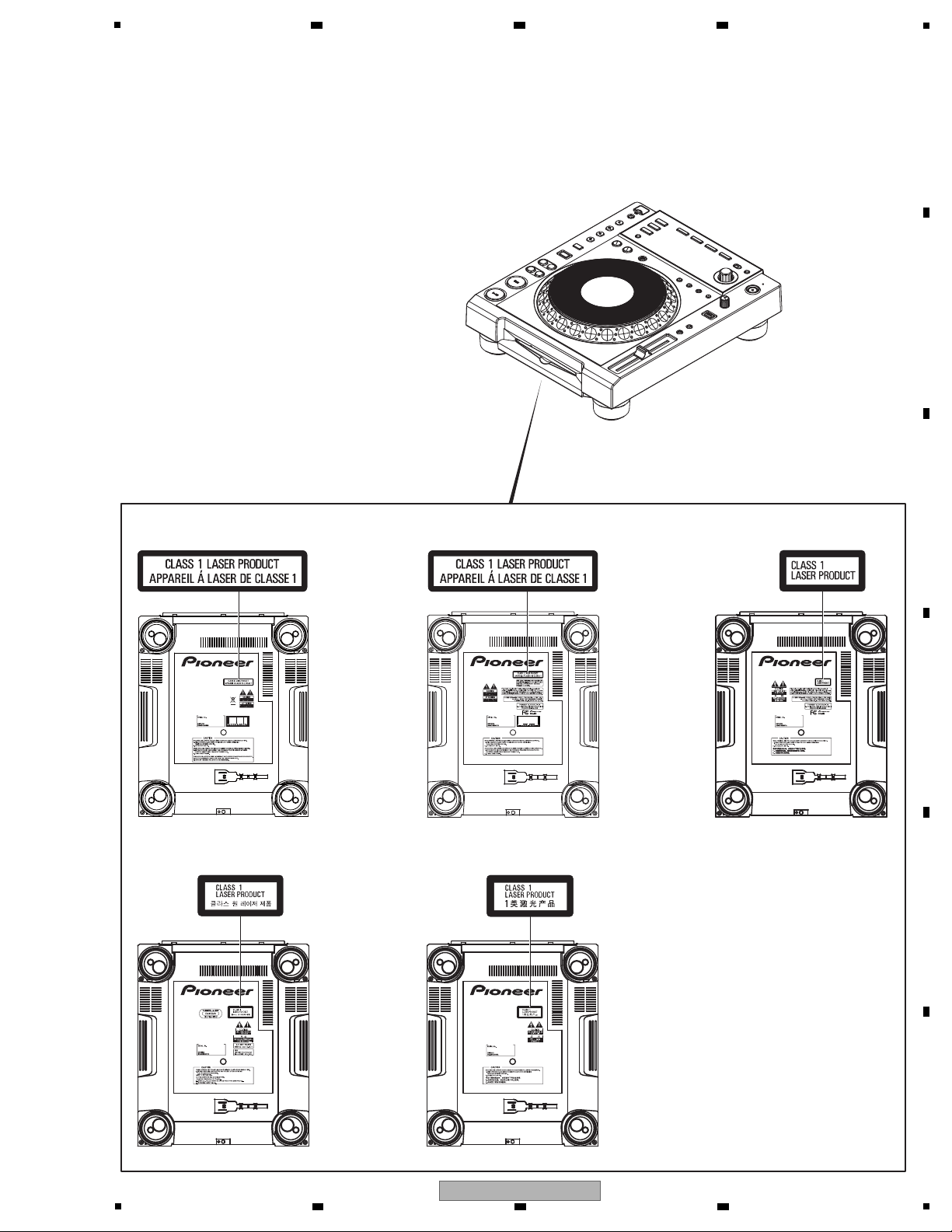
LABEL CHECK
(Printed on the chassis)
(Printed on the chassis) (Printed on the chassis)
(Printed on the chassis) (Printed on the chassis)
SYXJ8
KXJ5 AXJ5
CUXJ FLXJ
5
6 7 8
A
B
C
D
E
5
CDJ-850
6 7 8
F
3
1
[Important Check Points for Good Servicing]
In this manual, procedures that must be performed during repairs are marked with the below symbol.
Please be sure to confirm and follow these procedures.
1. Product safety
Please conform to product regulations (such as safety and radiation regulations), and maintain a safe servicing environment by
following the safety instructions described in this manual.
1 Use specified parts for repair.
Use genuine parts. Be sure to use important parts for safety.
2 Do not perform modifications without proper instructions.
Please follow the specified safety methods when modification(addition/change of parts) is required due to interferences such as
radio/TV interference and foreign noise.
3 Make sure the soldering of repaired locations is properly performed.
When you solder while repairing, please be sure that there are no cold solder and other debris.
Soldering should be finished with the proper quantity. (Refer to the example)
4 Make sure the screws are tightly fastened.
Please be sure that all screws are fastened, and that there are no loose screws.
5 Make sure each connectors are correctly inserted.
Please be sure that all connectors are inserted, and that there are no imperfect insertion.
6 Make sure the wiring cables are set to their original state.
Please replace the wiring and cables to the original state after repairs.
In addition, be sure that there are no pinched wires, etc.
7 Make sure screws and soldering scraps do not remain inside the product.
Please check that neither solder debris nor screws remain inside the product.
8 There should be no semi-broken wires, scratches, melting, etc. on the coating of the power cord.
Damaged power cords may lead to fire accidents, so please be sure that there are no damages.
If you find a damaged power cord, please exchange it with a suitable one.
9 There should be no spark traces or similar marks on the power plug.
When spark traces or similar marks are found on the power supply plug, please check the connection and advise on secure
connections and suitable usage. Please exchange the power cord if necessary.
a Safe environment should be secured during servicing.
When you perform repairs, please pay attention to static electricity, furniture, household articles, etc. in order to prevent injuries.
Please pay attention to your surroundings and repair safely.
2. Adjustments
To keep the original performance of the products, optimum adjustments and confirmation of characteristics within specification.
Adjustments should be performed in accordance with the procedures/instructions described in this manual.
4. Cleaning
For parts that require cleaning, such as optical pickups, tape deck heads, lenses and mirrors used in projection monitors, proper
cleaning should be performed to restore their performances.
3. Lubricants, Glues, and Replacement parts
Use grease and adhesives that are equal to the specified substance.
Make sure the proper amount is applied.
5. Shipping mode and Shipping screws
To protect products from damages or failures during transit, the shipping mode should be set or the shipping screws should be
installed before shipment. Please be sure to follow this method especially if it is specified in this manual.
A
2 3 4
B
C
D
E
F
4
1
CDJ-850
2 3 4

5
6 7 8
CONTENTS
SAFETY INFORMATION.......................................................................................................................................................... 2
1. SERVICE PRECAUTIONS ....................................................................................................................................................6
1.1 NOTES ON SOLDERING............................................................................................................................................... 6
1.2 ABOUT POWER SUPPLY MONITORING...................................................................................................................... 6
2. SPECIFICATIONS .................................................................................................................................................................7
2.1 SPECIFICATIONS .......................................................................................................................................................... 7
2.2 USABLE DISCS AND USB DEVICES............................................................................................................................ 8
2.3 PANEL FACILITIES....................................................................................................................................................... 10
3. BASIC ITEMS FOR SERVICE ............................................................................................................................................13
3.1 CHECK POINTS AFTER SERVICING .........................................................................................................................13
3.2 JIGS LIST .....................................................................................................................................................................13
3.3 PCB LOCATIONS ......................................................................................................................................................... 14
4. BLOCK DIAGRAM ..............................................................................................................................................................16
4.1 OVERALL WIRING DIAGRAM .....................................................................................................................................16
4.2 SIGNAL BLOCK DIAGRAM.......................................................................................................................................... 18
4.3 POWER SUPPLY BLOCK DIAGRAM........................................................................................................................... 20
5. DIAGNOSIS ........................................................................................................................................................................ 22
5.1 POWER ON SEQUENCE.............................................................................................................................................22
5.2 TROUBLESHOOTING.................................................................................................................................................. 23
5.3 DIAGNOSIS OF THE PICKUP ASSY........................................................................................................................... 32
5.4 CONNECTION CHECK WITH THE PC........................................................................................................................ 33
5.5 ABOUT POWER SUPPLY MONITORING.................................................................................................................... 34
5.6 ABOUT THE PROTECTORS........................................................................................................................................ 34
6. SERVICE MODE................................................................................................................................................................. 35
6.1 SERVICE MODE ................................................................................................................
6.2 ABOUT THE DEVICE OF CDJ-850..............................................................................................................................35
6.3 DETAILS ON SERVICE MODE .................................................................................................................................... 36
7. DISASSEMBLY ................................................................................................................................................................... 42
8. EACH SETTING AND ADJUSTMENT................................................................................................................................ 52
8.1 NECESSARY ITEMS TO BE NOTED...........................................................................................................................52
8.2 USER SETABLE ITEMS ............................................................................................................................................... 52
8.3 UPDATING OF THE FIRMWARE ................................................................................................................................. 53
8.4 JOG DIAL ROTATION LOAD ADJUSTMENT ............................................................................................................... 55
9. EXPLODED VIEWS AND PARTS LIST...............................................................................................................................56
9.1 PACKING SECTION ..................................................................................................................................................... 56
9.2 EXTERIOR SECION.....................................................................................................................................................58
9.3 CONTROL PANEL SECTION ....................................................................................................................................... 60
9.4 JOG DIAL SECTION .................................................................................................................................................... 62
9.5 SLOTIN MECHA SECTION.......................................................................................................................................... 64
10. SCHEMATIC DIAGRAM .................................................................................................................................................... 66
10.1 CNCT, SLMB and JINT ASSYS .................................................................................................................................. 66
10.2 MAIN ASSY (1/4)........................................................................................................................................................68
10.3 MAIN ASSY (2/4)........................................................................................................................................................70
10.4 MAIN ASSY (3/4)........................................................................................................................................................72
10.5 MAIN ASSY (4/4)........................................................................................................................................................74
10.6 CMPX (1/2) and USBA ASSYS .................................................................................................................................. 76
10.7 CMPX ASSY (2/2) ......................................................................................................................................................78
10.8 DFLB ASSY .....................................................................................................................
SW1 and KSW2 ASSYS .......................................................................................................................................... 82
10.9 K
10.10 JFLB and JOGB ASSYS...........................................................................................................................................84
10.11 SLD1, PSWB and SLD2 ASSYS ..............................................................................................................................86
10.12 POWER SUPPLY and ACIN ASSYS ........................................................................................................................ 88
10.13 VOLTAGES ............................................................................................................................................................... 90
10.14 WAVEFORMS...........................................................................................................................................................91
10.15 EACH SIGNAL LEVEL.............................................................................................................................................. 93
11. PCB CONNECTION DIAGRAM........................................................................................................................................94
11.1 CNCT, SLMB and JINT ASSYS .................................................................................................................................. 94
11.2 MAIN ASSY ................................................................................................................................................................ 98
11.3 CMPX and USBA ASSYS.........................................................................................................................................102
11.4 DFLB ASSY .............................................................................................................................................................. 106
SW1 and KSW2 ASSYS ........................................................................................................................................ 110
11.5 K
11.6 JFLB and JOGB ASSYS...........................................................................................................................................112
11.7 SLD1, PSWB and SLD2 ASSYS ..............................................................................................................................114
11.8 POWER SUPPLY and ACIN ASSYS ........................................................................................................................116
12. PCB PARTS LIST ............................................................................................................................................................ 118
.......................................... 35
........................................... 80
A
B
C
D
E
F
CDJ-850
5
6 7 8
5

1
• For environmental protection, lead-free solder is used on the printed circuit boards mounted in this unit.
Be sure to use lead-free solder and a soldering iron that can meet specifications for use with lead-free solders for repairs
accompanied by reworking of soldering.
• Compared with conventional eutectic solders, lead-free solders have higher melting points, by approximately 40 ºC.
Therefore, for lead-free soldering, the tip temperature of a soldering iron must be set to around 373 ºC in general, although
the temperature depends on the heat capacity of the PC board on which reworking is required and the weight of the tip of
the soldering iron.
Do NOT use a soldering iron whose tip temperature cannot be controlled.
Compared with eutectic solders, lead-free solders have higher bond strengths but slower wetting times and higher melting
temperatures (hard to melt/easy to harden).
The following lead-free solders are available as service parts:
• Parts numbers of lead-free solder:
GYP1006 1.0 in dia.
GYP1007 0.6 in dia.
GYP1008 0.3 in dia.
This unit always monitors for power failure and will shut itself off immediately after an error is detected. If an error is generated,
the STANDBY LED will flash after the unit shuts itself off. After the unit shuts itself off because of an error, unplug the AC power
cord and wait 1 minute before turning the unit ON by pressing the STANDBY/ON key.
Repair the unit, according to “5.5 ABOUT POWER SUPPLY MONITORING.”
2 3 4
1. SERVICE PRECAUTIONS
1.1 NOTES ON SOLDERING
A
B
C
1.2 ABOUT POWER SUPPLY MONITORING
D
E
F
6
1
2 3 4
CDJ-850

5
Power requirements........ AC 220 V to 240 V, 50 Hz/ 60 Hz (SYXJ8)
AC 120 V, 60 Hz (CUXJ)
AC 110 V to 240 V, 50 Hz/ 60 Hz (FLXJ)
AC 220 V, 60 Hz (KXJ5)
AC 220 V to 240 V, 50 Hz/ 60 Hz (AXJ5)
Power consumption................................................................... 21 W
Power consumption (standby).................................................. 0.4 W
Main unit weight....................................................................... 2.3 kg
Max. dimensions........ 305 mm (W) × 105.5 mm (H) × 364.4 mm (D)
(12 in. (W) × 4.2 in. (H) × 14.3 in. (D))
Tolerable operating temperature.............................. +5 °C to +35 °C
(+41 °F to +95 °F)
Tolerable operating humidity.............5 % to 85 % (no condensation)
Analog audio output (AUDIO OUT L/ R)
Output terminal.............................................................RCA terminal
Output Level........................................................... 2.0 Vrms (1 kHz)
Frequency response.................................................. 4 Hz to 20 kHz
S/ N ratio.................................................................................115 dB
Total harmonic distortion.......................................................0.003 %
USB downstream section (USB)
Port..........................................................................................Type A
Power supply.......................................................5 V/ 500 mA or less
USB upstream section (USB)
Port..........................................................................................Type B
Control output (CONTROL)
Port...................................................................................... Mini-jack
• The specifications and design of this product are subject to
change without notice.
2. SPECIFICATIONS
2.1 SPECIFICATIONS
6 7 8
A
B
C
D
E
F
CDJ-850
5
6 7 8
7
1
2 3 4
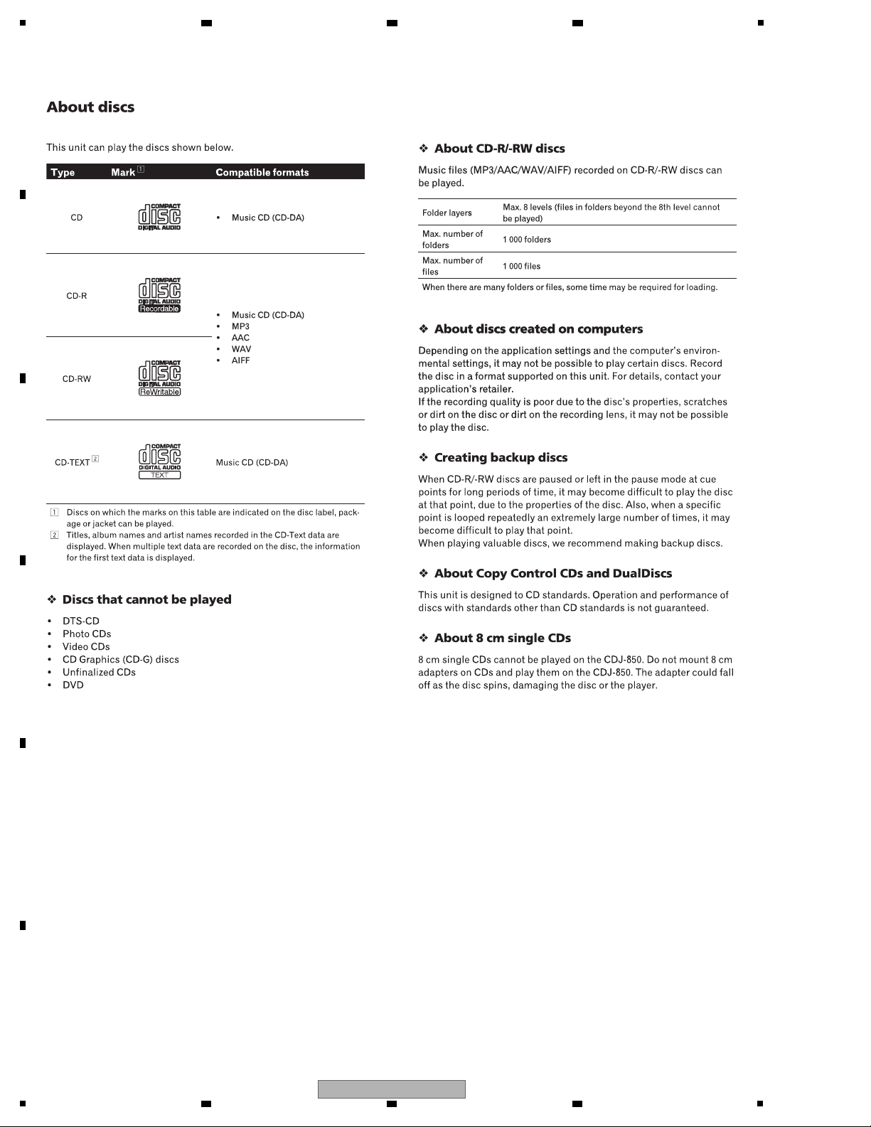
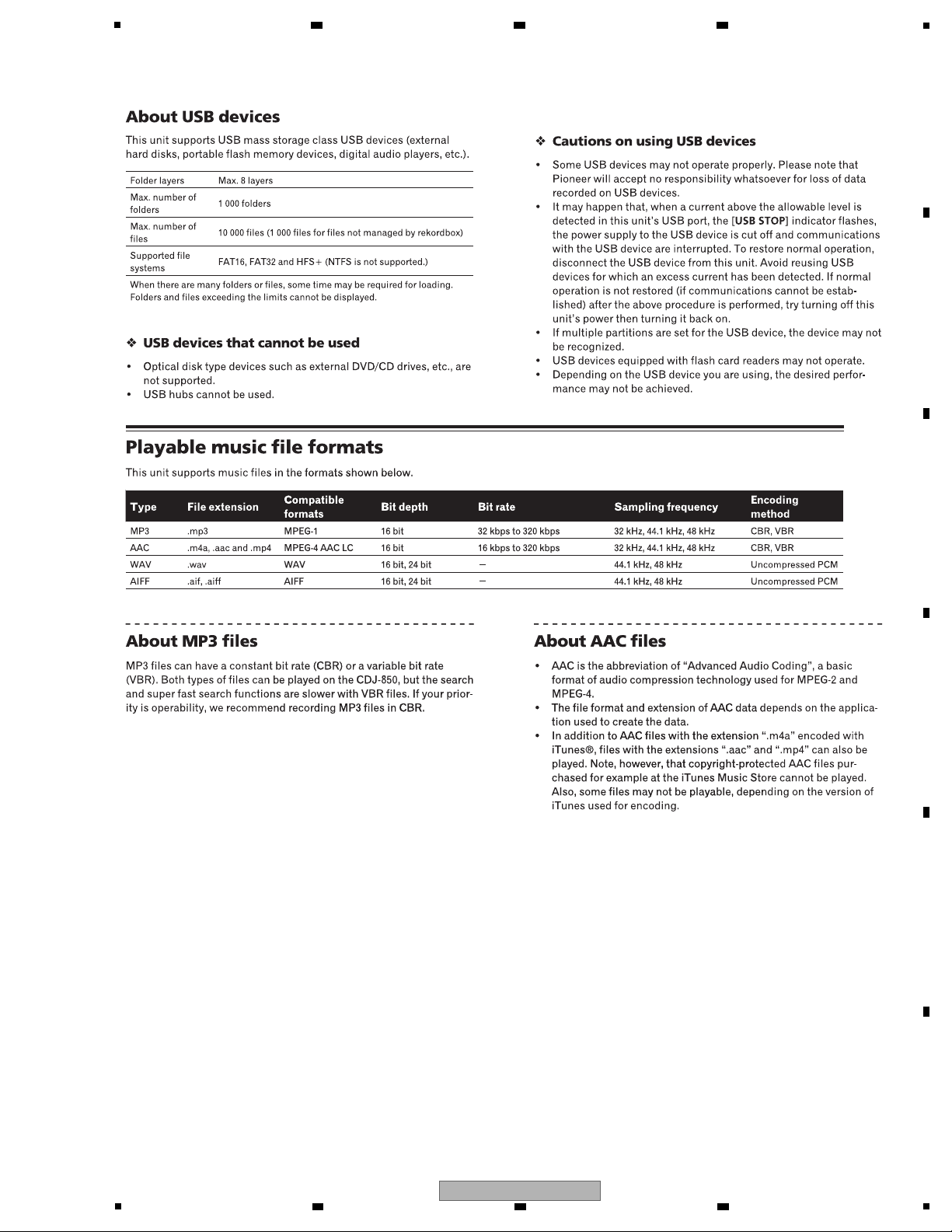
2.2 USABLE DISCS AND USB DEVICES
A
B
C
D
E
F
8
1
2 3 4
CDJ-850
5
6 7 8
A
B
C
D
E
F
CDJ-850
5
6 7 8
9
1
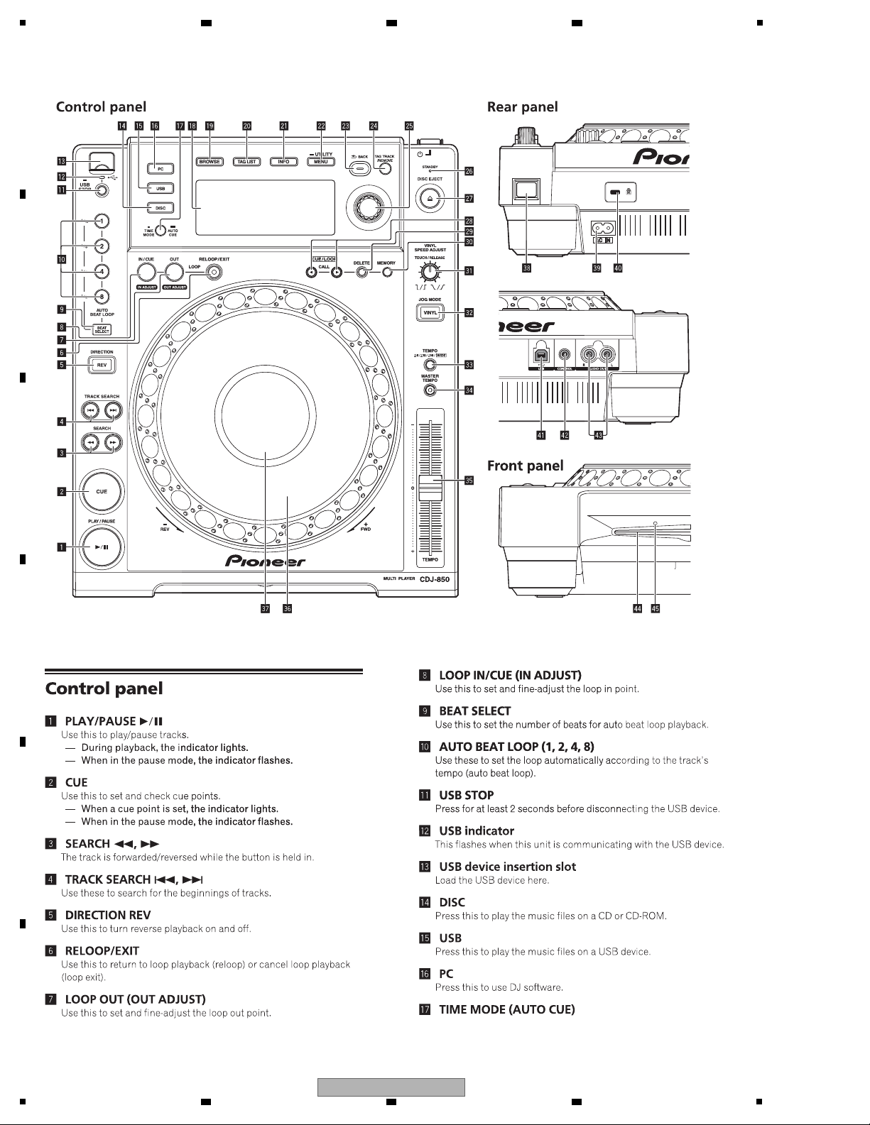
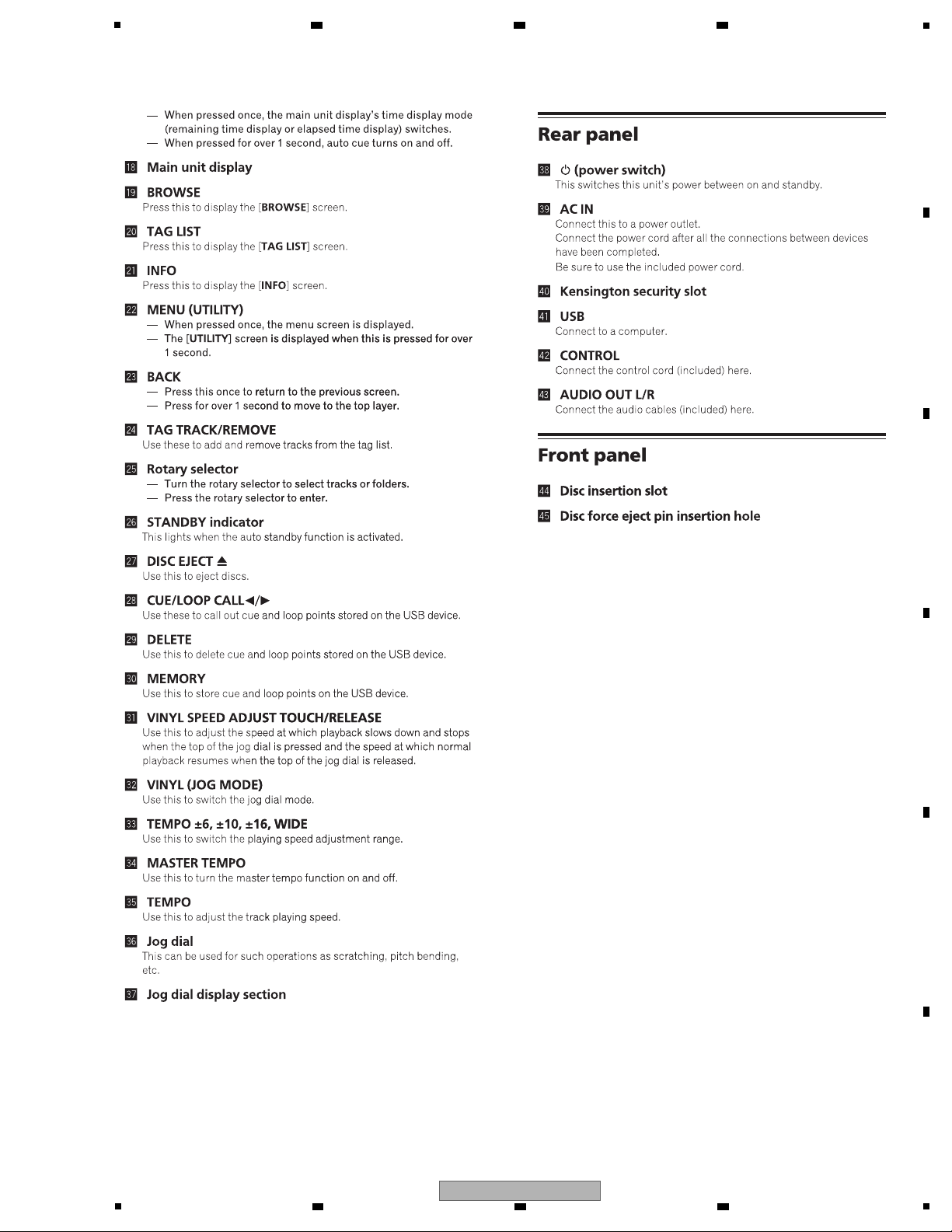
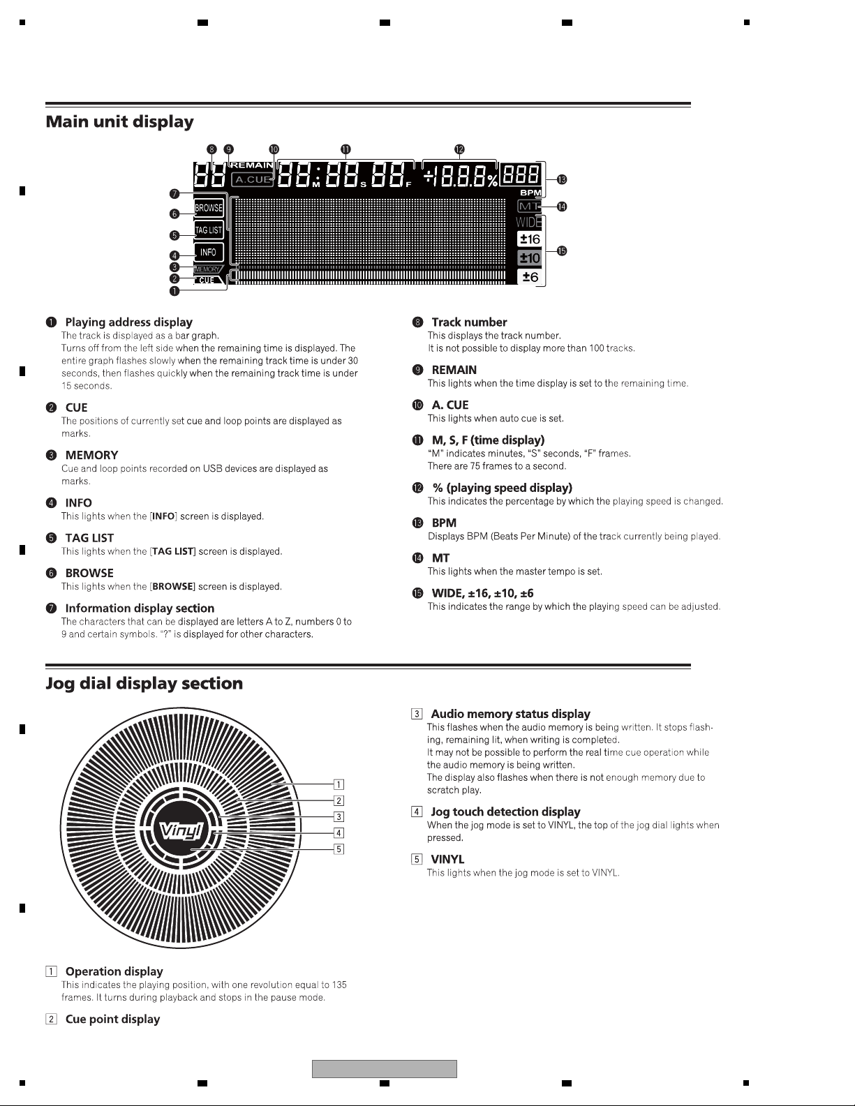
2.3 PANEL FACILITIES
A
B
2 3 4
C
D
E
F
10
1
2 3 4
CDJ-850
5
6 7 8
A
B
C
D
E
F
CDJ-850
5
6 7 8
11
1
A
B
2 3 4
C
D
E
F
12
1
2 3 4
CDJ-850
5
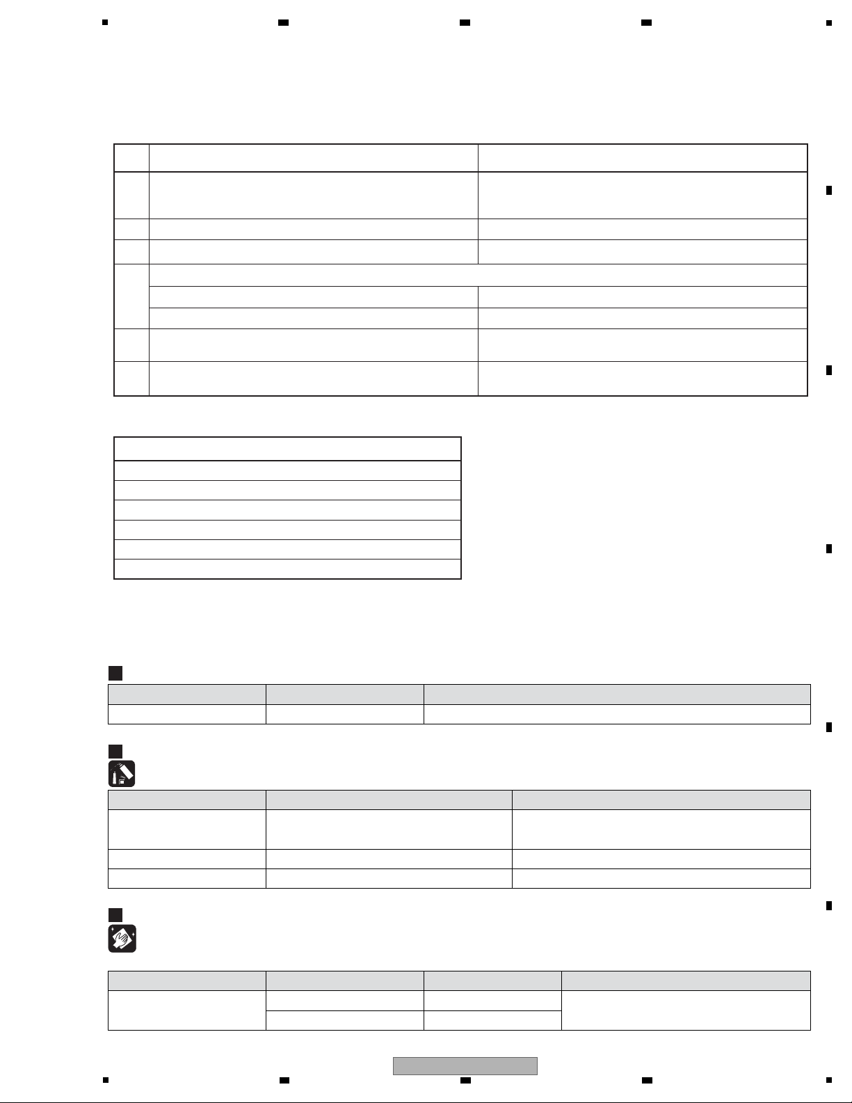
Items to be checked after servicing / CDJ
To keep the product quality after servicing, confirm recommended check points shown below.
No.
Procedures Check points
1
3
4
5
6
Confirm whether the customer complain has been solved.
If the customer complain occurs with the specific disc, use it for
the operation check.
The customer complain must not be reappeared.
Audio and operations must be normal.
Play back a CD. (track search) Audio, Search and operations must be normal.
2 Check output analog audio. Audio and operations must be normal.
Check the connection of each interface.
Play back data contained in the device connected to USB A. Audio, Search and operations must be normal.
USB B The device must be recognized by the PC.
Check output signals while the JOG dial or TEMPO slider is
being operated.
Audio and operations must be normal.
Check the appearance of the product.
No scratches or dirt on its appearance after receiving it for
service.
Item to be checked regarding audio
Distortion
Noise
Volume too low
Volume too high
Volume fluctuating
Sound interrupted
See the table below for the items to be checked regarding video and audio.
Cleaning
Name Part No. Remarks
Cleaning paper GED-008
Cleaning liquied GEM1004 Refer to
"9.5 SLOTIN MECHA SECTION".
Position to be cleaned
Pickup lenses
Jigs List
Jig Name Part No. Purpose of use / Remarks
CD test disc STD-905 CD playback diagnosis
Before shipping out the product, be sure to clean the following positions by using the prescribed cleaning tools.
Lubricants and Glues List
Name Part No. Remarks
Lubricating oil ZLB-HFD1600 Refer to “9.4 JOG DIAL SECTION”.
Dyfree GEM1036 Refer to “9.5 SLOTIN MECHA SECTION”.
Lubricating oil GYA1001
Refer to “9.4 JOG DIAL SECTION”,
“9.5 SLOTIN MECHA SECTION”.
6 7 8
3. BASIC ITEMS FOR SERVICE
3.1 CHECK POINTS AFTER SERVICING
A
B
3.2 JIGS LIST
5
6 7 8
CDJ-850
C
D
E
F
13
1
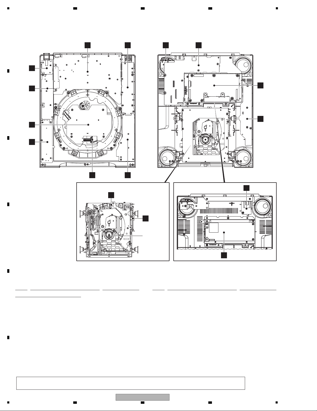
1..MAIN ASSY DWX3174
NSP 1..SUB1 ASSY (SYXJ8, FLXJ, KXJ5, AXJ5) DWM2399
NSP 1..SUB1 ASSY (CUXJ) DWM2405
NSP 2..KSW1 ASSY DWS1422
NSP 2..SLD1 ASSY DWS1423
2..PSWB ASSY DWS1424
2..SLMB ASSY DWS1425
2..KSW2 ASSY DWS1426
2..SLD2 ASSY DWS1427
2..DFLB ASSY DWX3152 ∗
2..JFLB ASSY DWX3154
2..JOGB ASSY DWX3155
2..ACIN ASSY (SYXJ8, FLXJ, KXJ5, AXJ5) DWX3158
2..ACIN ASSY (CUXJ) DWX3173
NSP 1..SUB2 ASSY DWM2400
2..CNCT ASSY DWX3151
2..CMPX ASSY DWX3153
2..USBA ASSY DWX3156
2..JINT ASSY DWX3157
> 1..POWER SUPPLY ASSY DWR1463
NSP 1..SLOTIN MECHA ASSY DXA2206
1..TM ASSY-S (VTM091) DXX2616
E
CMPX ASSY
G
DFLB ASSY
H
KSW1 ASSY
F
USBA ASSY
O
POWER SUPPLY ASSY
I
KSW2 ASSY
K
JOGB ASSY
B
SLMB ASSY
P
ACIN ASSY
• Bottom view
A
CNCT
ASSY
TM ASSY-S
(VTM091)
C
JINT
ASSY
J
JFLB
ASSY
L
SLD1
ASSY
N
SLD2
ASSY
M
PSWB
ASSY
D
MAIN
ASSY
SLOTIN MECHA ASSY
Mark No. Description Part No. Mark No. Description Part No.
LIST OF ASSEMBLIES
NOTES: - Parts marked by “NSP” are generally unavailable because they are not in our Master Spare Parts List.
-
The > mark found on some component parts indicates the importance of the safety factor of the part.
Therefore, when replacing, be sure to use parts of identical designation.
∗
The service part of DFLB Assy (DWX3152) is supplied with KSW1 Assy (DWS1422) and SLD1 Assy (DWS1423).
(There assemblies are connected with the jumper wires.)
3.3 PCB LOCATIONS
A
2 3 4
B
C
D
E
F
14
1
2 3 4
CDJ-850

5
6 7 8
A
B
C
D
E
F
CDJ-850
5
6 7 8
15
1
ADG7022 (For CUXJ)
ADG7097, ADG1154 (For FLXJ)
XDG3054 (For KXJ5)
ADG1154 (For SYXJ8)
ADG7079 (For AXJ5)
ACIN ASSY
(DWX3173: CUXJ)
(DWX3158: OTHERS)
P
DKP3891: CUXJ
DKP3889: OTHERS
I
H
KSW2
(DWS
KSW1 A
(DWS1
B
C
SLMB ASSY
(DWS1425)
O
POWER SUPPLY
ASSY
(DWR1463)
JINT ASSY
(DWX3157)
A
CNCT ASSY
(DWX3151)
CMPX ASSY
(DWX3153)
E
E E
1/2, 2/2
MAIN ASSY
(DWX3174)
D
D D
1/4- 4/4
!
!
AKM1299-A
CN401
1
V+7R6_M2GNDM
3
GNDD4GNDD5GNDD
6
V+7R6_D7V+7R6_D
8
GNDD
9
V+12
10
GNDD
11
V-10_A
12
GNDA
13
V+10_A
B6B-XH-A
1
GNDM
2
GNDD
3
PWR_XON
4
V+12
5
V+12
6
V+12_EUP
B2P3-VH
1
LIVE(PURPLE)
2
NEUTRAL(BLUE)
1V+6R6
2GNDD
3CUE_LED
4CUE_SW
5PLAY_LED
1
ST1-
2
ST1+
3
ST2+
4
ST2-
1
FR
2
FD
3
TR
4
TD
5
NC
6
GNDS
7
LD650
8
PD
9
LD780
10
GNDS
11
VR780
12
VRCOM
13
VR650
14
A
15
B
16
VRF
17
SW1_DVD/CD
18
C
19
D
20
E
21
Vcc
22
VREF
23
F
24
GNDS
DKN1445-A
CN2302
GNDS
1
V+5P
2
F
3
VREF
4
E
5
D
6
C
7
GNDS
8
GNDS
9
B
10
A
11
GNDS
12
GNDS
13
VR780PD
14
GNDS
15
GNDS
16
GNDS
17
GNDS
18
LD780
19
GNDS
20
TD
21
TR
22
FD
23
FR
24
DKN1312-A
CN2301
1
INSW
2
W
3
V
4
U
5
HB
6
W-
7
W+
8
V-
9
V+
10
U-
11
U+
12
VCC
CN2304
DKN1288-A
ST1-
1
ST1+
2
ST2+
3
ST2-
4
DKN1445-A
CN2501
FR
1
FD
2
TR
3
TD
4
NC
5
GNDS
6
LD650
7
PD
8
LD780
9
GNDS
10
VR780
11
VRCOM
12
VR650
13
A
14
B
15
VRF
16
SW1_DVD/CD
17
C
18
D
19
E
20
Vcc
21
VREF
22
F
23
GNDS
24
DKN1445-A
CN2502
1
GNDS
2
V+5P
3
F
4
VREF
5
E
6
D
7
C
8
GNDS
9
GNDS
10
B
11
A
12
GNDS
13
GNDS
14
VR780PD
15
GNDS
16
GNDS
17
GNDS
18
GNDS
19
LD780
20
GNDS
21
TD
22
TR
23
FD
24
FR
CN1701
VKN 1265-A
LPS21
LPS12
GNDD3
LO+4
LO-5
RKN1058-A
CN403
1
GNDD
2
GNDD
3
VBUS_B
4
GNDD
5
USB_D_P
6
USB_D_N
7
GNDD
8
CONT2
9
GNDD
10
CONT1
11
GNDD
12
GNDD
13
GNDA
14
LOUT
15
GNDA
16
ROUT
17
GNDA
RKN1068-A
CN402
1
USBA_D_P
2
USBA_D_N
3
GNDD
4
USB_CODETFLG
5
GNDD
6
USB_VBUSON
7
GNDD
8
PWR_ON
9
GNDD
10
VDET
11
GNDD
12
MAIN_XMUTE
13
GNDD
14
MAIN_XRST
15
TSI
16
MAIN_XBUSY
17
TSO
18
PNL_XBUSY
19
GNDD
20
TSCK
21
GNDD
22
V+5R6
23
V+5R6
24
GNDD
25
GNDD
26
V+12_EUP
27
GNDD
KM200NA13
CN2004
1
V+7R6_M
2
GNDM
3
GNDD
4
GNDD
5
GNDD
6
V+7R6_D
7
V+7R6_D
8
GNDD
9
V+12
10
GNDD
11
V-10_A
12
GNDA
13
V+10_A
B6B-XH-A
CN2001
1
GNDM
2GNDD
3PWR_XON
4V+12
5V+12
6V+12_EUP
VKN1252-A
CN2003
1
TSO
2
PNL_XBUSY
3
TSI
4
GNDD
5
TSCK
6
GNDD
7
PNL_CNVSS
8
GNDD
9
PNL_XRST
10
MAIN_XBUSY
11
USB_STOP
12
MAIN_XRST
13
PWR_ON
14
PNL_XMUTE
15
VDET
16
GNDD
17
V+12
18
V+12
19
GNDD
20
V+12_EUP
21
GNDD
VKN 1258-A
CN2002
CN1
CN2
1
GNDD
2
V+12_EUP
3
GNDD
4
GNDD
5
V+5R6
6
V+5R6
7
GNDD
8
TSCK
9
GNDD
10 PNL_XBUSY
11 TSO
12
MAIN_XBUSY
13 TSI
14
MAIN_XRST
15
GNDD
16
MAIN_XMUTE
17
GNDD
18
VDET
19
GNDD
20 PWR_ON
21
GNDD
22
USB_VBUSON
23
GNDD
24 USB_CODETFLG
25
GNDD
26 USBA_D_N
27 USBA_D_P
VKN1248-A
CN2006
1
GNDA
2
ROUT
3
GNDA
4
LOUT
5
GNDA
6
GNDD
7
GNDD
8
CONT1
9
GNDD
10
CONT2
11
GNDD
12
USB_D_N
13
USB_D_P
14
GNDD
15
VBUS_B
16
GNDD
17
GNDD
CN2005
52147-0510
1
V+5_USB
2
USBA_D_N
3
USBA_D_P
4
GNDD
5
GNDD
51048-0500
JH2201
1
V+5_USB
2
USBA_D_N
3
USBA_D_P
4
GNDD
5
GNDD
JA2401
1
2
DKN1407-A
CN2305
1
INSW
2
W
3
W
4
V
5
V
6
U
7
U
8
GNDD
9
HW-
10
HW+
11
HV-
12
HV+
13
HU-
14
HU+
15
V+5M
16
GNDD
17
FR
18
FD
19
TR
20
TD
21
GNDS
22
LD780
23
GNDS
24
PD
25
A_A
26
A_B
27
A_C
28
A_D
29
A_S1
30
VREF
31
A_S2
32
V+5P
33
GNDS
34
GNDS
35
GNDS
36
LPS1
37
LPS2
38
GNDS
39
LO-
40
LO-
41
LO+
42
LO+
43
ST2+
44
ST2+
45
ST2-
46
ST2-
47
ST1+
48
ST1+
49
ST1-
50
ST1-
DKN1404-A
CN201
1
ST1-
2
ST1-
3
ST1+
4
ST1+
5
ST2-
6
ST2-
7
ST2+
8
ST2+
9
LO+
10
LO+
11
LO-
12
LO-
13
GNDS
14
LPS2
15
LPS1
16
GNDS
17
GNDS
18
GNDS
19
V+5P
20
A_S2
21
VREF
22
A_S1
23
A_D
24
A_C
25
A_B
26
A_A
27
PD
28
GNDS
29
LD780
30
GNDS
31
TD
32
TR
33
FD
34
FR
35
GNDD
36
V+5M
37
HU+
38
HU-
39
HV+
40
HV-
41
HW+
42
HW-
43
GNDD
44
U
45
U
46
V
47
V
48
W
49
W
50
INSW
CN2303
VKN 1374-A
1
LPS2
2
LPS1
3
GNDD
4
LO+
5
LO-
1
INSW
2
W
3
V
4
U
5
HB
6
W-
7
W+
8
V-
9
V+
10
U-
11
U+
12
VCC
NEUTRAL
LIVE
SPINDLE MOTOR
09SD PICK UP ASSY
DDD1527Pitch=1.0mm
Length=180mm
Same Face
FFC
DDD1491Pitch=0.5mm
Length=175mm
Reverse Face FFC
ZWNN1007G28-9-06A
Length=60mm
White Single Wire
ZWNN1007G28-8-06A
Length=60mm
Gray Single Wire
LO-
LO-
LO+
LO+
LOADING MOTOR
ASSY-S
(DXX2615)
Pitch=1.0mm
Reverce Face
FFC
DDD1536-(Gold)
Pitch=0.5mm
Length=66mm
Reverse Face FFC
PF13PP-S07
Pitch=2.0mm
Length=75mm
Connector Ass'y
DDD1524Pitch=1.0mm
Length=70mm
Same Face
FFC
DDD1523Pitch=1.0mm
Length=70mm
Same Face
FFC
D20PDY07
Pitch=2.0m
Length=20
Parallel Ju
DDD1522Pitch=1.0mm
Length=170mm
Same Face
FFC
D20PDY0510E
Pitch=2.0mm
Length=100mm
Parallel Jumper
Wire
DE010VE0
Length=100mm
Earth Lead Cable
Horizontal
Contact Side Down
Vertical
Horizontal
AC POWER CORD
Vertical
Contact Side
Vertical
Contact Side
Vertical
Vertical
VH
Soldered
DKP3869Pitch=2.5mm
Length=100mm
Connector Assy
DKP3870Pitch=3.96mm
Length=100mm
Connector Ass'y
US
Pitch=1.0mm
Same Face
FPC
STEPPING
MOTOR
Horizontal
Contact Side Up
Vertical
Contact Side
Horizontal
Contact Side Up
Horizontal
Contact Side Down
Horizontal
Contact Side Down
Horizontal
Contact Side Down
Horizontal
Contact Side Down
Horizontal
Contact Side Down
Horizontal
Contact Side Up
Horizontal
Contact Side Up
Boardin
Vertical
Vertical
Vertical
Verti
Vertical
Contact Side
Soldered
DDD1535Pitch=0.5mm
Length=80mm
Reverse Face FFC
SLOTIN MECHA ASSY
(DXA2206)
TM ASSY-S (DXX2616)
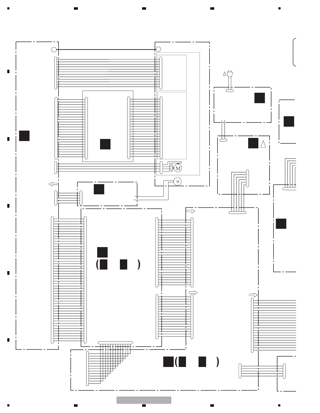
4. BLOCK DIAGRAM
4.1 OVERALL WIRING DIAGRAM
A
16
1
B
C
D
E
F
2 3 4
2 3 4
CDJ-850
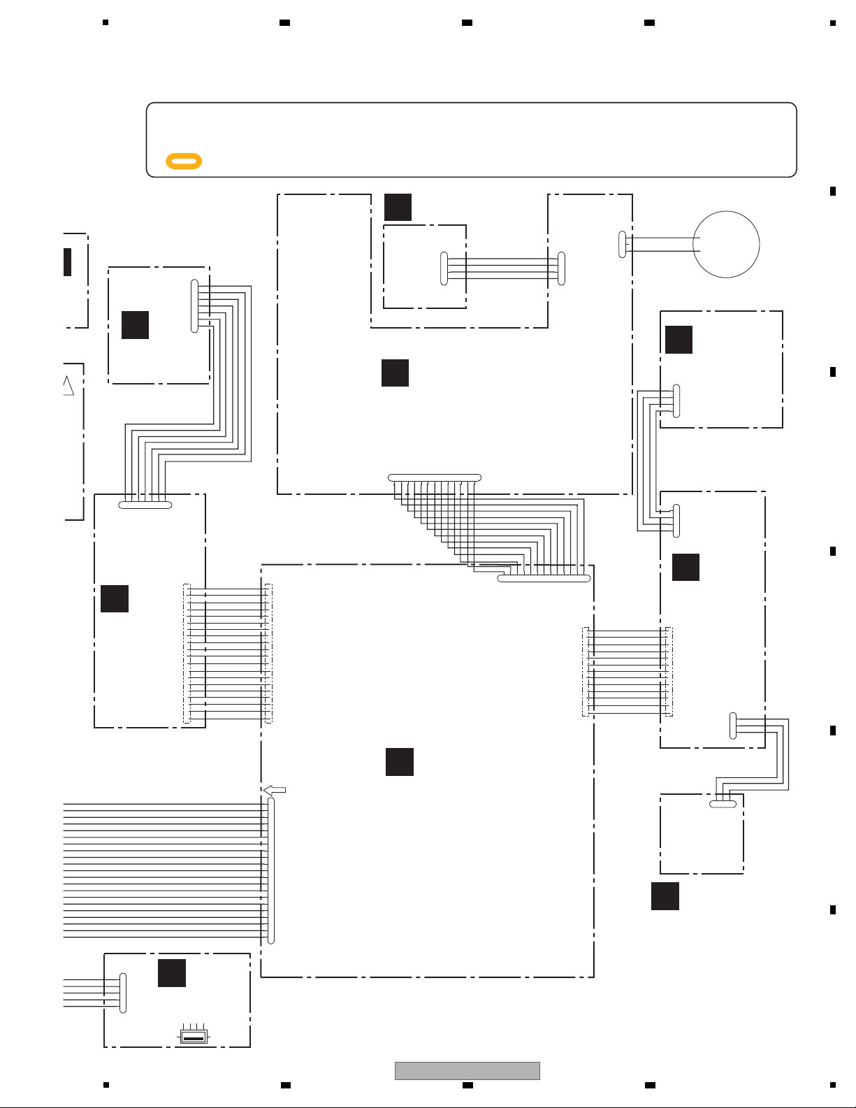
5
-
When ordering service parts, be sure to refer to "EXPLODED VIEWS and PARTS LIST" or "PCB PARTS LIST".
-
The > mark found on some component parts indicates the importance of the safety factor of the part.
Therefore, when replacing, be sure to use parts of identical designation.
-
: The power supply is shown with the marked box.
G
DFLB ASSY
(DWX3152)
I
H
KSW2 ASSY
(DWS1426)
F
USBA ASSY
(DWX3156)
K
JOGB ASSY
(DWX3155)
N
SLD2 ASSY
(DWS1427)
L
SLD1 ASSY
(DWS1423)
KSW1 ASSY
(DWS1422)
J
JFLB ASSY
(DWX3154)
LY
M
PSWB ASSY
(DWS1424)
!
CN1801
CKS1072-A
1JOG_SW
2N C
3G NDD
52147-0710
CN1401
1
V+6R6
2
GNDD
3
CUE_LED
4
CUE_SW
5
PLAY_LED
6
PLAY_SW
7
KEY2_B
VKN 1273-A
CN1002
1V +12
2GNDD
3V +38
4GNDD
5JOG1
6JOG2
7JOG_SW
8J_DSO
9J_BK
10J_SCLK
11J_LAT
12GNDD
13V+3R3_SW
CN1901
52151-0410
1
JOG2
2
JOG1
3
V+3R3_SW
4
GNDD
CN1601
52147-0310
1PWR_SW
2GN DD
3GN DD
CN1501
52147-0410
1
ADCT
2
ADIN
3
GNDA
4
V+3R3_EUP
DKB1106-1
JA2201
1
234
RT1
RT2
51048-0700
JH1201
1V+6R6
2GNDD
3CUE_LED
4CUE_SW
5PLAY_LED
6PLAY_SW
7KEY2_B
51048-0400
JH1801
1
JOG2
2
JOG1
3
V+3R3_SW
4
GNDD
51048-0400
JH1301
1 ADCT
2 ADIN
3GNDA
4 V+3R3_EUP
51048-0300
JH1302
1
PWR_SW
2
GNDD
3
GNDD
51048-0500
JH2201
1
V+5_USB
2
USBA_D_N
3
USBA_D_P
4
GNDD
5
GNDD
VKN 1252-A
CN1001
1
GNDD
2
V+12_EUP
3
GNDD
4
V+12
5
V+12
6
GNDD
7
VDET
8
PNL_XMUTE
9
PWR_ON
10
MAIN_XRST
11
USB_STOP
12
MAIN_XBUSY
13
PNL_XRST
14
GNDD
15
PNL_CNVSS
16
GNDD
17
TSCK
18
GNDD
19
TSI
20
PNL_BUSY
21
TSO
VKN 1244-A
CN1802
1
V+3R3_SW2GNDD
3 J_LAT
4
J_SCLK
5
J_BK
6
J_DSO7JOG_SW
8 JOG2
9 JOG1
10
GNDD
11
V+38
12
GNDD
13
V+12
D20PDY0720E
Pitch=2.0mm
Length=200mm
Parallel Jumper Wire
D20PDY0410E
Pitch=2.0mm
Length=100mm
Parallel Jumper Wire
D20PDY0310E
Pitch=2.0mm
Length=100mm
Parallel Jumper Wire
D20PYY0405E
Pitch=2.0mm
Length=50mm
Parallel Jumper Wire
DDD1522Pitch=1.0mm
Length=170mm
Same Face
FFC
ngth=100mm
re
DDD1521Pitch=1.0mm
Length=120mm
Same Face
FFC
Jumper Wire
Horizontal
ADIN
PWR_SW
MT_LED
ADCT
EJECT_LED
TCH/REL
KEY0
VIN YL_LED
ADIN
PWR_SW
MT_LED
ADCT
EJECT_LED
TCH/REL
VIN YL_LED
KEY0
EUP_LED
EUP_LED
GNDD
GNDD
V+6R6
V+6R6
V+3R3_EUP
V+3R3_EUP
GNDA
GNDA
SHIFT_SW
1KEY_SW
USB_ACT_LED
REV_SW
8KEY_LED
1KEY_LED
4KEY_SW
4KEY_LED
REV_LED
USB_STOP
8KEY_SW
2KEY_SW
2KEY_LED
PLAY_LED
PLAY_SW
GNDD
CUE_LED
V+6R6
CUE_SW
KEY2_B
4KEY_LED
USB_STOP
8KEY_SW
2KEY_SW
2KEY_LED
KEY2_B
PLAY_LED
SHIFT_SW
CUE_LED
GNDD
PLAY_SW
REV_LED
CUE_SW
1KEY_SW
USB_ACT_LED
REV_SW
8KEY_LED
V+6R6
1KEY_LED
4KEY_SW
Vertical
Contact Side Up
Horizontal
Contact Side Up
Horizontal
Contact Side Up
Jumper Wire
Vertical
Vertical
Vertical
Vertical
Vertical
Vertical
Vertical
Vertical
Vertical
Contact Side
SHEET SW
(DSX1078)
6 7 8
A
B
C
D
5
6 7 8
CDJ-850
E
F
17
1
IC105
Buffer
PICKUP ASSY
JA2002
CONTROL
IC101
32M
FLASH ROM
IC302
DAC
IC301
DSP
IC103
MAIN CPU
CLK: 33 MHz
CORE CLK:
200 MHz
IC102
256M
SDRAM
IC303
OP AMP
7
1
JH2201
IC201
SERVO
DSP
IC204
DRIVER
OEIC
M
LOADING
MOTOR
M
STEPPING
MOTOR
12
15
1
2
3
5
10
13
14
PNL_XMUTE
3 2
CN2005
13
18
24
8
10
12
14
16
20
22
USB_CODETFLG
USB_VBUSON
PNL_XBUSY
TSO
MAIN_XBUSY
TSI
MAIN_XRST
MAIN_XMUTE
VDET
PWR_ON
TSCK
26
27
VBUS_B
3
3
CN1701
CN2301
CN2302
CN2303
CN2304
7
8
16
System Bus (Bus CLK:66MHz)
IC107
USB SW
X102
X-tal
48MHz
X101
X-tal
33MHz
JA2001
USB Type B
CONNECTOR
JA2003
AUDIO OUT
JA2003
USB Type A
CONNECTOR
K
1
SPINDLE
MOTOR
1
INSW
LD780
SHORT
SW
9
LD780
1
2
1
2
LPS2
LPS1
15
14
50
LPS1
LPS2
INSIDE
29
DP
DM
15
10
4
20
18
17
16
14
12
8
6
2
1
5
14
16
10
8
6
3
3
2
MUTE
CIRCUIT
VBUS
1
1
IC2003
USB OVER
CURRENT
PROTECT
POWER DETECT
CIRCUIT
13
4
2
8
10
12
15
CONT2
CONT1
USBB_D_N
USBB_D_P
USBA_D_N
USBA_D_P
USBA_D_N
USBA_D_P
V+5_USB
V+5_USB
3
5
16
16
36
37
1
22
CN2501CN2502
135
134
136 94
93 1
3
3
1
56
55
USB_X2
USB_X1
XTAL
EXTAL
LOUT
ROUT
66
70
64
48
75
59
88
71
USB_CDETFLG
MUTE
87
4
5
USB_ABSEL
LDO
ST1+,ST1-,ST2+,ST2-
LO+,LO-
W,V,U,HB,W-,W+,V-,V+,U-,U+
ST1+,ST1-,
ST2+,ST2-
LO+,LO-
W,V,U,HB,W-,W+,
V-,V+,U-,U+
VR780PD,
A,B,C,D,E,F
ALO
ARO
FR,FD,TR,TD
FR,FD,TR,TD
X103
X-tal
16.9344
MHz
5
6
210
CLK11M
USB
Full Speed
I/F
SCIF
DACBCLK,
DACBCLK,
DACBCLK
DRVMUTE1,
DRVMUTE2,
PWMLO,
PWMSL1IN,
PWMSL2IN
SPDLFG
TCOUNT,
ADC
DSPCS,DSPRST,PLAY
ZERO
45
73
43 181
161 185
102
100
101
208
113
160
3
5
10
1
7
2
6
149
150
15 11
41
73
16
DACCS
AUDIO_SCK,
AUDIO_SI,
AUDIO_SO
BCK,
LRCK,
DATA_L,
DATA_R
SRVSCLK,
SRVLRCK,
SRVSDATA
SRVBCLK,SRVBUS0-3,
SRVSBSY,SRVCCE,
SRVRST
11
JA2401
CN2001
CN2004
CN401
CN2002
CN402
CN2305
CN201
CN403
CN2006
CONT2
CONT1
LOUT
ROUT
PWR_XON
CN2003
JH120
CN140
119
P
ACIN ASSY
I
H
KS
E
CMPX ASSY
B
SLMB ASSY
A
CNCT ASSY
D
MAIN ASSY
C
JINT ASSY
F
USBA
O
POWER SUPPLY
ASSY
VR780PD,A,B,C,D,E,F
CLK_S_16M
CLK_A_16M
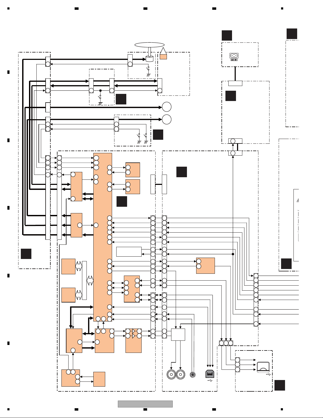
4.2 SIGNAL BLOCK DIAGRAM
A
2 3 4
B
C
D
E
F
18
2 3 4
1
CDJ-850
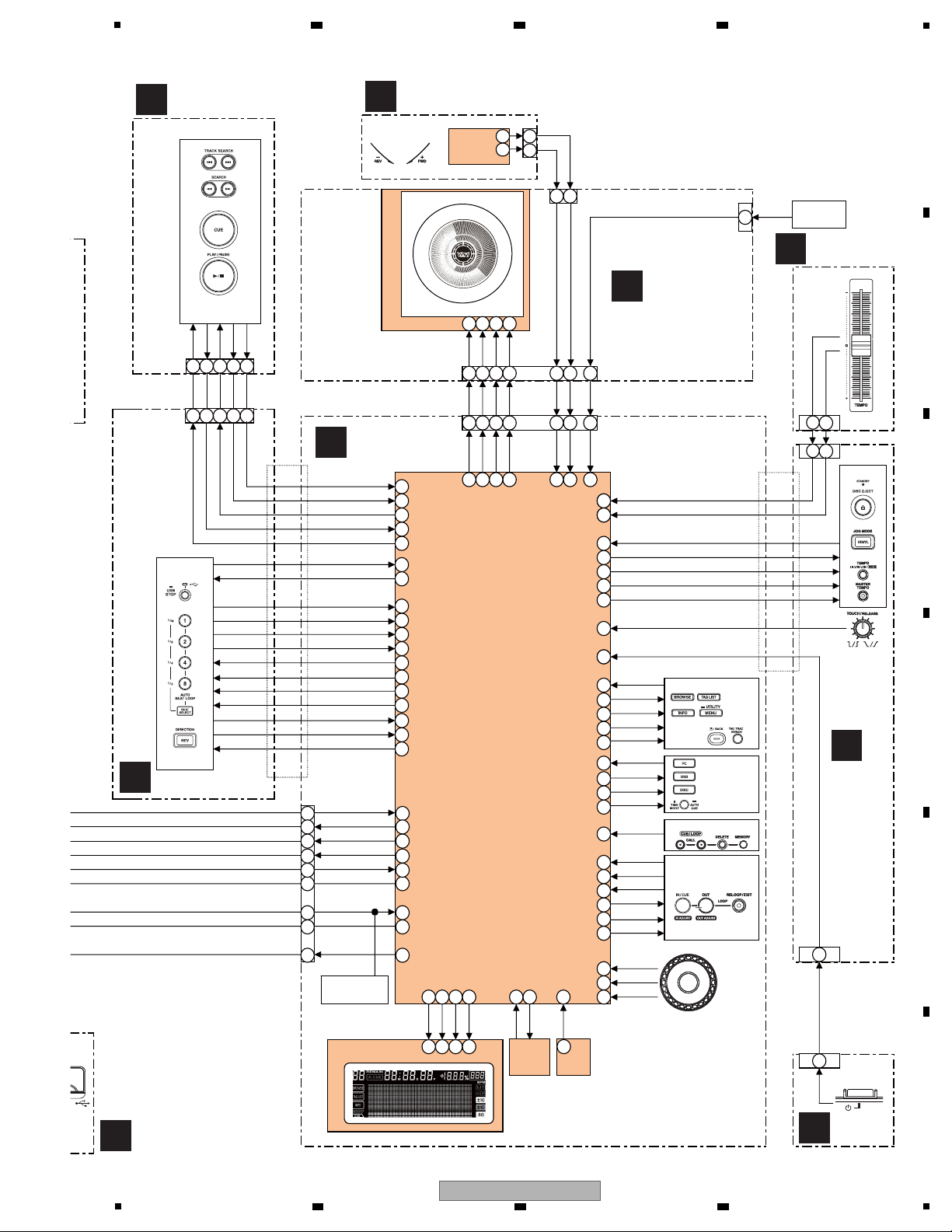
IC1007
PANEL CPU
CLK: 15.975 MHz
JOG2
JOG1
PWR_SW
CN1601
PC1901
ENCODER
4
3
2
1
VR8701
TEMPO SLIDER
98
6
4
JOG_SW
JH1801
1
1
1
1
1
2
ADIN
ADCT
3 5 7
ADIN
ADCT
PLAY_SW
7
64
KEY2_B
PLAY_LED
CUE_SW
CUE_LED
3 5
76
4
3 5
VDET
PNL_XMUTE
PNL_XBUSY
TSI
TSCK
MAIN_XBUSY
MAIN_XRST
PWR_ON
TSO
X1001
X-tal
15.975 MHz
VR1301
TOUCH/RELEASE
PWR_SW
90
2
1
5
68
10
11
9 7
2625242321 28 27
ENC_2
ENC_1
ENC_SW
5
4
3
S1018
KEY,LED
83
60
58
61
59
CUE_LED
CUE_SW
PLAY_LED
PLAY_SW
KEY2
TCH/REL
88
KEY,LED
EUP_LED1
EJECT_LED
KEY0
VINYL_LED
MT_LED
TCH/REL
92
93
87
94
95
EUP_LED
EJECT_LED
KEY0
VINYL_LED
MT_LED
3937
38
323133
35
30
XOUT
XIN
LOOPIN_SW
56
63
65
66
67
68
4KEY_LED
8KEY_LED
REV_LED
SHIFT_SW
REV_SW
69
70
1KEY_LED
2KEY_LED
71
72
4KEY_SW
8KEY_SW
73
2KEY_SW
74
57
USB_STOP
1KEY_SW
75
USB_ACT_LED
KEY,LED
1
2
KEY,LED
IN_LED
55
54
53
52
51
76
82
LOOPOUT_SW
OUT_LED
RELOOP_LED
RELOOP_SW
DISC_LED
UTILITY_LED
80
79
78
77
PLAYLIST_LED
BROWSE_LED
PC_LED
USB_LED
81
84
INFO_LED
85
86
KEY4
KEY1
KEY3
1
DATA FL
JOG FL
24252726
40
32
34
31
33
42
44
45
43
10
7
21
20
19
17
12
9
8
JUMPER
JUMPER
IC1004
RESET IC
1215
4
13
PNL_XRST
1
2
POWER DETECT
CIRCUIT
KEY,LED
KEY,LED
KEY,LED
SHEET SW
CN1001
JH1201
CN1401
CN1901
CN1802
CN1002
JOG_SW
JOG1
JOG2
JOG_SW
JOG1
JOG2
J_DSO
J_BK
J_SCLK
J_LAT
J_DSO
J_BK
J_SCLK
J_LAT
D_BK
D_LAT
D_SCLK
D_DSO
ROTARY SW
JH1302
PWR_SW
JH1301
CN1501
CN1801
I
KSW2 ASSY
H
KSW1 ASSY
K
JOGB ASSY
J
JFLB ASSY
G
DFLB ASSY
N
SLD2 ASSY
L
SLD1
ASSY
M
PSWB ASSY
F
USBA ASSY
V1801
5
V100
6 7 8
A
B
C
D
E
F
CDJ-850
5
6 7 8
19
1
A
CNCT ASSY
P
ACIN ASSY
I
K
H
KSW
E
CMPX ASSY
B
SLMB ASSY
D
MAIN ASSY
C
JINT
ASSY
F
USBA AS
O
POWER
SUPPLY
ASSY
IC105
Buffa
JA2002
CONTROL
IC101
32M
FLASH ROM
IC302
DAC
IC301
DSP
IC103
MAIN CPU
IC102
256M
SDRAM
IC303
OP AMP
JH2201
IC201
SERVO DSP
IC204
DRIVER
OEIC
M
LOADING
MOTOR
M
STEPPING
MOTOR
V+
18
CN2003
CN2005
20
PWR_ON
3
3
CN1701
CN2301
CN2302
CN2303
CN2304
IC107
USB SW
JA2001
USB Type B
CONNECTOR
JA2003
AUDIO OUT
JA2003
USB Type A
CONNECTOR
12
SPINDLE
MOTOR
12
2 2 21
21
8
MUTE
CIRCUIT
1
1
IC2003
USB OVER CURRENT
PROTECT (1A)
POWER DETECT CIRCUIT
V+5_USB
32
CN2501CN2502
17
20
13
PW
2
26
V+12_EUP
622
523
V+5R6
11
V+7R6_M
V+7R6_D
V+12
V+10_A
V-10_A
13
7
7
1
9
5 6
65
V+1
IC2001
DCDC
12V→7.6V
12V→-11V
Q2028
REGULATOR
12V→10V
Q2028
REGULATOR
-11V→-10V
66
VCC
22
4
V+5P
VREF
VCC
VREF
V+5P
VREF
V+5M
19
30
21
15 36
IC409
DCDC
7.6V→5.6V
IC401
REGULATOR
5.6V→3.3V
IC402
REGULATOR
5.6V→3.3V
IC405
REGULATOR
5.6V→5V
IC206
REGULATOR
7.6V→5.6V
IC404
REGULATOR
3.3V→1.2V
IC408
REGULATOR
5.6V→3.3V
IC403
REGULATOR
3.3V→1.25V
IC406
REGULATOR
10V→5V
13
11
15
VD
ACDC
18
10
IC2002
REGULATOR
5.6V→5V
1
9
12
4
4
224
PICKUP ASSY
V+7R6_M
V+7R6_D
V+12
V+10_A
V-10_A
V+10_A
V-10_A
VREF1R65
V+5P
V+5M
V+
V-11_A
P2003
PROTECTOR
(0.5A)
P2004
(0.375A)
VDET
VDET
V+7R6
V+5R6
V+3R3
V+3R3_S
V+5R6_M
V+1R2
V+3R3_A
V+1R25
V+5_A
CN2305
CN201
CN403
CN2006
V+5_USB
V-11_A
V+12_EUP
CN2002
CN402
CN401
CN2004
CN2001
PWR_XON
V+12
V+12_EUP
JA2401
CN140
JH120
PROTECTOR
2 3 4
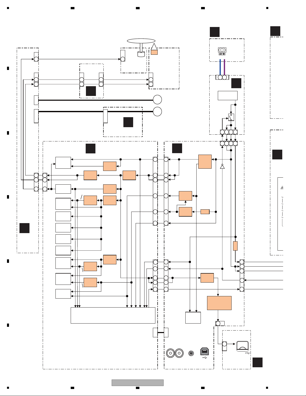
4.3 POWER SUPPLY BLOCK DIAGRAM
A
B
C
D
E
F
20
1
2 3 4
CDJ-850

5
I
KSW2 ASSY
H
KSW1 ASSY
K
JOGB ASSY
J
JFLB ASSY
G
DFLB ASSY
N
SLD2 ASSY
L
SLD1
ASSY
M
PSWB ASSY
F
USBA ASSY
IC1007
PANEL CPU
CN1601
PC1901
ENCODER
VR8701
TEMPO SLIDER
JH1801
1
4
1
1
V+3R3_EUP
1
1
CN1001
V+12
VR1301
TOUCH/RELEASE
S1018
ROTARY SW
LED
LED
LED
4
LED
DATA FL
JOG FL
23
4
JUMPER
JUMPER
IC1004
RESET IC
POWER DETECT CIRCUIT
LED
LED
LED
V+3R3_SW
3
1
38
1
13 11
V+27
IC1802
DCAC
12V→AC2.7V
IC1803
DCDC
12V→27V
VFDP2R7_F1
V+6R6
V+3R3_EUP
V+6R6
5
2
IC1006
DCDC
12V→6.6V
IC1006
DCDC
12V→3.3V
Q1018
FET SW
V+3R3_EUP
V+3R3_EUP
V+3R3_SW
9
PWR_ON
V+12_EUP
VDET
7
131 3
1
34
35
2
3
V+12
V+12_EUP
V+12
V+6R6
V+3R3_SW
V+6R6
V+27_SW
V+3R3_SW
V+38
V+3R3_EUP
PWR_SW
PWR_SWPWR_SW
V+38
PWR_ON
3
3
V+6R6
CN1401
JH1201
V+6R6
V+38
V+3R3_SW
V+6R6_FL
V1001
VDET
CN1002
CN1802
V1801
V+38
V+3R3_SW
V+12
CN1901
CN1801
SHEET SW
CN1501
JH1301
JH1302
VDET
PWR_ON
6 7 8
A
B
C
D
CDJ-850
5
6 7 8
E
F
21
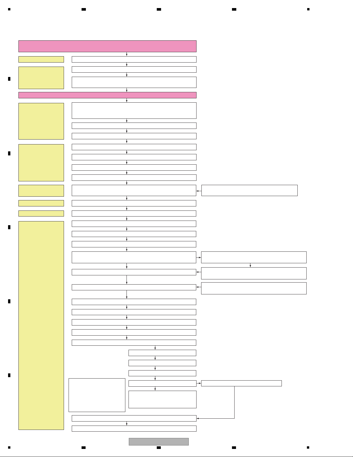
1
If the level of the S-shaped waveform is 0.88 Vp-p or less,
focusing is turned ON with RF gain increased.
If checking fails three times, “EJECT” will be
displayed on the FL display.
The first track is searched for.
After TOC reading is completed
Waiting 300 ms
Tracking balance adjustment (Tracking open)
Tracking close
GFS (RF lock) check
Main CPU (IC103)
Panel CPU (IC1007)
Adjustment of tracking and focus offset
Spindle kick, focus sweep, and focus ON
Checking if focus is OK
Audio DSP (IC301)
Servo DSP (IC201)
CD drive
Playback (Muting OFF)
Focus gain adjustment
AC IN (Plugging of the AC power cord)
Power supply (V+12_EUP, V+3R3R_EUP) to the Panel CPU starts.
Reset IC (IC1004)
TOC reading
Depending on the accuracy
of the stepper, the TOC
position memory will be
located after the unit is
turned ON.
Tracking gain adjustment
RF gain adjustment
If the pickup is reading the
program area, it will jump
to the TOC area.
The program is downloaded to IC301 (Audio DSP).
IC103 (Pin 158): The Reset signal is sent to the Audio DSP (IC301).
IC301 (Pin 47): Receives the Reset signal.
IC1007 (Pin 12): Receives the Reset signal.
IC1004 (Pin 4): The Reset signal is sent to the Panel CPU (IC1007).
POWER ON (Turn on the POWER switch.)
Main CPU
(IC103)
STANDBY mode is entered.
*FL display: Unlit.
Panel CPU
(IC1007)
Panel CPU
(IC1007)
IC1007 (Pin 45): Power supply to the Main CPU (IC103) starts.
IC1007 (Pin 40): The Reset signal is sent to the Main CPU (IC103).
IC103 (Pin 69): The Reset signal is sent to the Servo DSP (IC201).
If communication fails, “E–8709” will be
displayed on the FL display.
STANDBY mode is shifted to POWER_ON mode.
“POWER ON” is displayed on the FL display.
Focus balance adjustment
IC103 (Pin 59): Receives the Reset signal.
Communication between the Main CPU (IC103) and
Panel CPU (IC1007) starts.
IC201 (Pin 90): Receives the Reset signal.
Checking the inside SW
LD (Laser Diode) ON
Acceleration of spindle (200 ms)
CLV servo ON
If the first check fails, measure the level of the S-shaped
waveform while the pickup lens is descending.
5. DIAGNOSIS
5.1 POWER ON SEQUENCE
A
2 3 4
B
C
D
E
F
22
1
CDJ-850
2 3 4
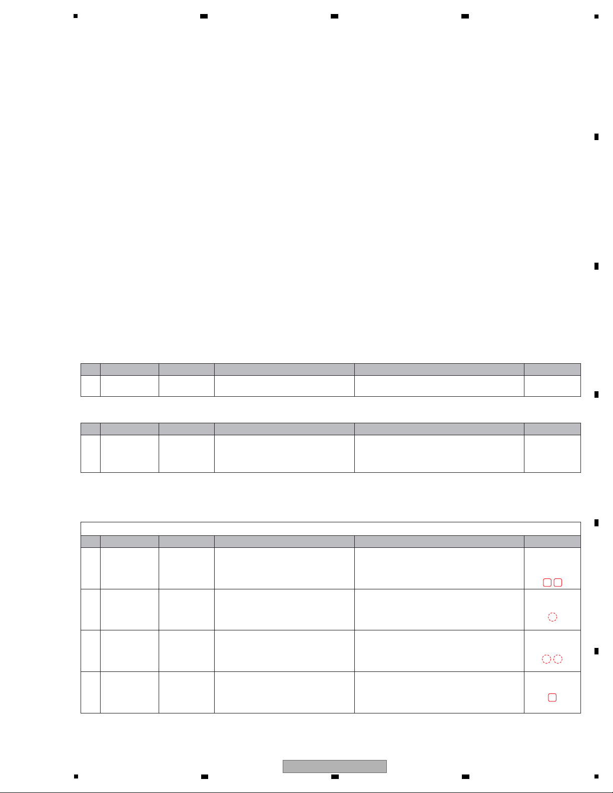
5
In this section, causes of failure, diagnostics points, and corrective measures can be searched for according to symptoms.
Before disassembling this unit, it is recommended to infer a failure point by referring to the error code.
For the relationship of each power-supply and signal system, see “4.3 POWER SUPPLY BLOCK DIAGRAM.”
If software of the product is updated before performing diagnostics, check that software updating has been performed properly
before proceeding to diagnostics.
If software updating has not been performed properly, update the software, following the instructions in “8.3 UPDATING OF
THE FIRMWARE.”
Contents
[0] Prior Confirmation
[1] Failure in Startup
[2] Display (DATA FL/JOG FL/LED)
[3] Operations (SW/Volume/JOG)
[4] USB (USB-Type A), PC (USB-Type B)
[5] AUDIO OUT
[6] CONTROL
[7] DRIVE Assy
[8] SERVICE MODE
[9] Error Codes
[10] Basic Operation Check of CPU/DSP
The waveform numbers described in this section correspond to the “10.14 WAVEFORMS.”
[0] Prior Confirmation
[0-1] Checking in Service Mode
[0-2] Checking Cables
[1] Failure in Startup
[1-1] No power
No. Cause
Diagnostics Point
Item to be Checked Corrective Action Reference
No. Cause
Diagnostics Point
Item to be Checked Corrective Action Reference
No. Cause
Diagnostics Point
Item to be Checked Corrective Action Reference
1 — Check the failure points.
See the section describing locations of defects in
this manual.
6. SERVICE
MODE
1 Cables
Service mode
Disconnection,
breakage, or
loose connection
of cables
Check that all the cables are securely
connected.
Check that there is no breakage in the
cables.
Securely connect the cables. If a cable is broken,
replace it.
4.1 OVERALL
CONNECTION
DIAGRAM
4.3 POWER SUPPLY
BLOCK DIAGRAM
10.13 VOLTAGES
Plug the AC power cord in and even if turn the power on, the product does not startup.
1
Standby power
failure
CMPX Assy
DFLB Assy
POWER
SUPPLY Assy
Check the voltages of V+12_EUP and
V+3R3_EUP.
If the V+12_EUP voltage is not output, the POWER
SUPPLY Assy may be defective.
If the V+12_EUP voltage is output, the DFLB Assy
may be defective.
10.15 EACH
SIGNAL LEVEL
2
Path failure of
the power switch
DFLB Assy
SLD1 Assy
PSWB Assy
Check if there is loose connection on the
signal line from the Power switch (S1601)
to PANEL CPU (IC1007).
If the connection up to the Power switch is properly
made and if the PWR_SW signal is not set to "L"
when the Power switch is pressed, the Power switch
may be defective.
10.15 EACH
SIGNAL LEVEL
3
Path failure of
the power on
DFLB Assy
CMPX Assy
Check the level of PWR_ON (IC1007-pin
45) and PWR_XON (CN2001-pin 3) signals.
If the PWR_ON is "L", PANEL CPU(IC1007) may be
defective.
If the PWR_XON is "H", poor connection or Q2021
may be defective.
10.13 VOLTAGES
4 Power failure
CMPX Assy
POWER
SUPPLY Assy
Check the V+12 voltage of CN2001-pins
4 and 5.
If the voltage is not output, POWER SUPPLY Assy
may be defective.
2
1 18
B J
A
6 7 8
5.2 TROUBLESHOOTING
A
B
C
D
E
F
CDJ-850
5
6 7 8
23
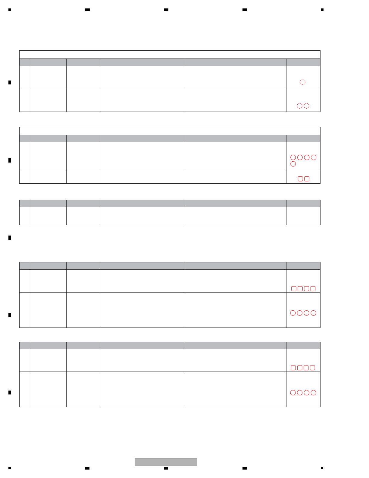
1
[1-2] Mode shift error in Standby mode
[2-1] The DATA FL does not light.
[2-2] The JOG FL does not light.
[2] Display (DATA FL/JOG FL/LED)
[1-3] “E-8709” is displayed on the DATA FL display after startup.
[1-4] The Standby LED flashes in red.
Shifting to the STANDBY mode cannot be performed even if turn the power off.
1
Path failure of
the power switch
DFLB Assy
SLD1 Assy
PSWB Assy
Check if there is loose connection on the
signal line from the Power switch (S1601)
to PANEL CPU (IC1007).
If the connection up to the Power switch is properly
made and if the PWR_SW signal is not set to "H"
when the Power switch is turned off, the Power switch
may be defective.
2
Path failure of
the power on
DFLB Assy
CMPX Assy
Check the level of PWR_ON (IC1007-pin
45) and PWR_XON (CN2001-pin 3) signals.
If the PWR_ON is "H", PANEL CPU(IC1007) may be
defective.
If the PWR_XON is "L", poor connection or Q2021
may be defective.
10.14
WAVEFORMS
1 Power failure DFLB Assy
Check the power-supply voltages
(V+6R6,F±, V+38, V+3R3_SW) of the FL.
If the presence of power is not confirmed, check the
mounting statuses of the regulator IC and its
peripheral parts for each power supply. If they are
properly mounted, then the parts may be defective.
4.3 POWER SUPPLY
BLOCK DIAGRAM
10.13 VOLTAGES
2 Signal errors DFLB Assy
Check the waveforms and connection of
communication line of FL in the DFLB Assy.
• D_SCLK
• D_SO
• D_LAT
• D_BK
If no signal is output, the PANEL CPU (IC1007) may
be defective.
If output signal is no problem, DATA FL (V1001) may
be defective.
10.14
WAVEFORMS
1 Power failure JFLB Assy
Check the power-supply voltages
(VFDP2R7_F1, VFDP2R7_F2, V+27,
V+3R3_SW) of the FL.
If the presence of power is not confirmed, check the
mounting statuses of the regulator IC and its
peripheral parts for each power supply. If they are
properly mounted, then the parts may be defective.
4.3 POWER SUPPLY
BLOCK DIAGRAM
10.13 VOLTAGES
2 Signal errors JFLB Assy
Check the waveforms and connection of
communication line of FL in the JFLB Assy.
• J_SCLK
• J_SO
• J_LAT
• J_BK
If no signal is output, the PANEL CPU (IC1007) may
be defective.
If output signal is no problem, JOG FL (V1801) may
be defective.
10.13 VOLTAGES
5.5 ABOUT POWER
SUPPLY MONITORING
10.13 VOLTAGES
10.14
WAVEFORMS
Communication between the Main CPU and Panel CPU has not been established.
1
Communication
failure between
the microcomputer
DFLB Assy
MAIN Assy
Check the TSCK, TSI, PNL_BUSY, TSO and
MAIN_BUSY waveforms.
If no signal is output, the possible causes are poor
connection, failure in the PANEL CPU (IC1007) or
MAIN CPU (IC103), and startup failure of the
MAIN CPU caused by defective FLASH ROM
(IC101) or SDRAM (IC102).
1
A voltage error
was generated.
— Check the level of the VDET signal.
If the signal level is "L", a voltage error was
generated.
2 Power failure MAIN Assy
Check the V+3R3 and V+1R2 power
voltages.
If power is not output, a part of the power supply
section may be defective.
10.15 EACH
SIGNAL LEVEL
10.15 EACH
SIGNAL LEVEL
No. Cause
Diagnostics Point
Item to be Checked Corrective Action Reference
No. Cause
Diagnostics Point
Item to be Checked Corrective Action Reference
No. Cause
Diagnostics Point
Item to be Checked Corrective Action Reference
No. Cause
Diagnostics Point
Item to be Checked Corrective Action Reference
No. Cause
Diagnostics Point
Item to be Checked Corrective Action Reference
20 21 23 19
24 25 22 19
9 10
B J
A
849 7 10
1 4 3 2
1 4 3 2
A
2 3 4
B
C
D
E
F
24
CDJ-850
1
2 3 4
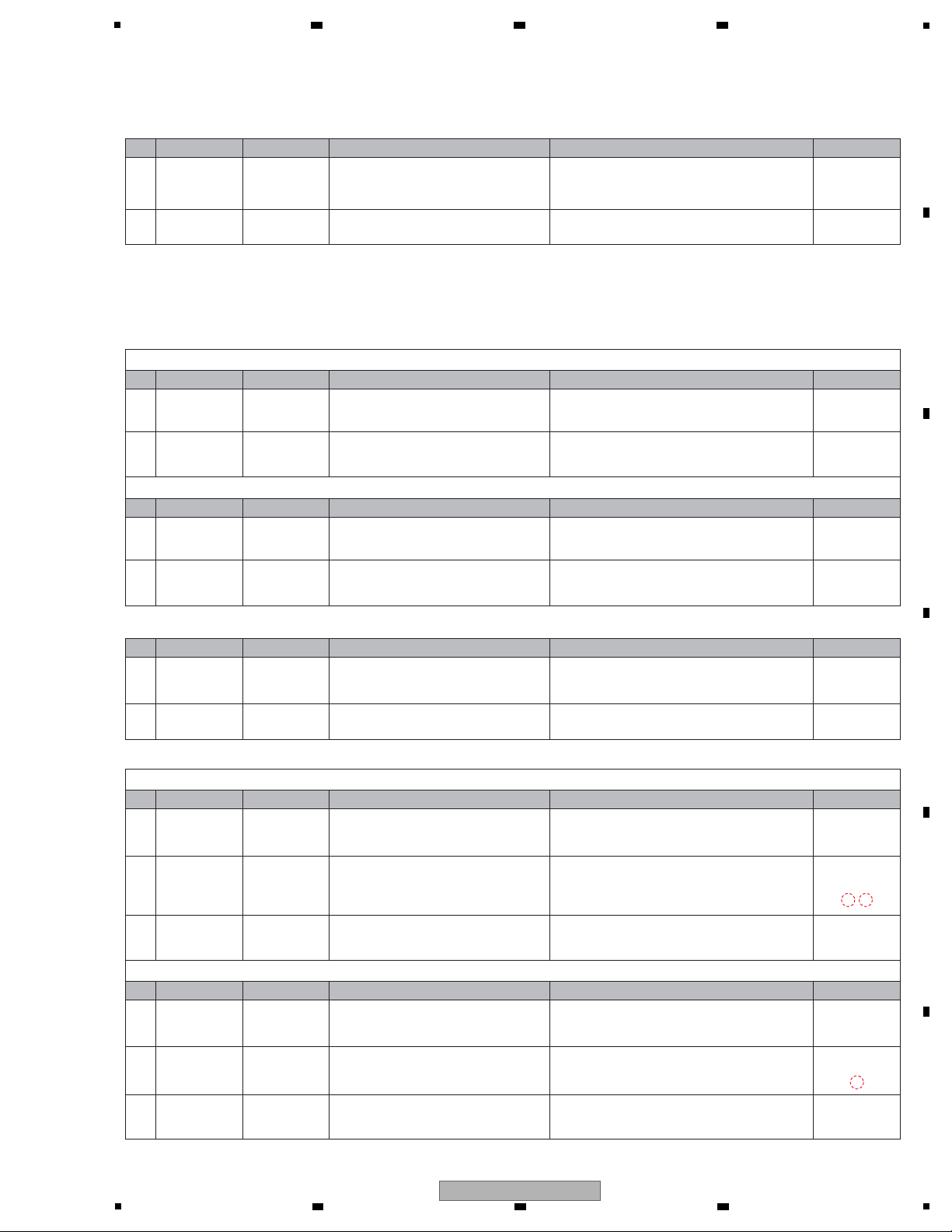
5
[2-3] The LED does not light.
—
[3] Operations (Keys/variable controls/JOG)
As operations of all keys, variable controls, and JOG dial can be checked in Service mode.
[3-1] No key functions
PLAY, CUE, AUTO BEAT LOOP 1-4, BEAT SELECT, REV, LOOP IN/OUT, RELOOP, or USB STOP key does not function.
1
Loose connection
/Defective SW
Related point
Check if there is loose connection on the
signal line from the PANEL CPU (IC1007)
up to the SW.
If there is no loose connection and if the signal does
not become "L" when the SW is pressed, that SW is
defective.
2
Defective PANEL
CPU (IC1007)
DFLB Assy
If the symptom persists after the above
corrections,
Check a mounting state of PANEL CPU (IC1007).
If the mounting is OK, the IC1007 may be defective.
The signals from other keys are analog and connected to multiple switches.
1
Loose connection
/Defective SW
Related point
Check if there is loose connection on the
signal line from the PANEL CPU (IC1007)
up to the SW.
If the SWs connected to the signal line function
properly and if the connections are properly made,
the SWs may be defective.
2
Defective PANEL
CPU (IC1007)
DFLB Assy
If the symptom persists after the above
corrections,
Check a mounting state of PANEL CPU (IC1007).
If the mounting is OK, the IC1007 may be defective.
[3-2] Rotary selector not controllable
1
Defective rotary
selector
DFLB Assy
Check if the signals from the RENC_1, RENC
_2, and RENC_SW signal lines are normal
when the rotary selector is turned or pressed.
If the signals are not normal, check the connections of
the signal lines. If the connections are properly made,
the Rotary selector (S1018) may be defective. Replace it.
2
Defective PANEL
CPU (IC1007)
DFLB Assy
If the symptom persists after the above
corrections,
Check a mounting state of PANEL CPU (IC1007).
If the mounting is OK, the IC1007 may be defective.
[3-3] Variable controls not controllable
Tempo slider not controllable
1
Loose
connection
DFLB Assy
SLD1 Assy
SLD2 Assy
Check if there is loose connection on the
signal line from the PANEL CPU (IC1007)
to the tempo slider (VR1501).
If the connections of signal line are improper,
resolder it.
2
Defective tempo
slider
DFLB Assy
SLD2 Assy
Check the ADCT and ADIN signals level.
If the voltage of the ADCT signal (IC1007-pin 1) is not
1.65 V, or the voltage of the ADIN signal (IC1007-pin 2)
does not change between 3.3 V and 0 V, the Tempo
slider (VR1501) may be defective.
3
Defective PANEL
CPU (IC1007)
DFLB Assy
If the symptom persists after the above
corrections,
Check a mounting state of PANEL CPU (IC1007).
If the mounting is OK, the IC1007 may be defective.
1 Signal errors DFLB Assy
Check that the control signal for the LED
is output from the PANEL CPU (IC1007).
If no signal is output, check a mounting state of
PA NEL CPU(IC1007). If the mounting is OK, the
IC1007 may be defective.
[10] Basic operation
check of CPU/DSP
[10] Basic operation
check of CPU/DSP
—
—
[10] Basic operation
check of CPU/DSP
[10] Basic operation
check of CPU/DSP
[10] Basic operation
check of CPU/DSP
2 Defective parts DFLB Assy
Check that the voltage (2.2 V) is present
at both ends of the LED.
If the voltage is abnormal, the LED, transistor or
peripheral resistors may be defective.
10.15 EACH
SIGNAL LEVEL
10.15 EACH
SIGNAL LEVEL
10.15 EACH
SIGNAL LEVEL
VINYL SPEED ADJUST not controllable
1
Loose
connection
DFLB Assy
SLD1 Assy
Check if there is loose connection on the
signal line from the PANEL CPU (IC1007) to
the VINYL SPEED ADJUST VR (VR1301).
If the connections of signal line are improper,
resolder it.
2
Defective
variable
controls
DFLB Assy
SLD1 Assy
Check the TCH/REL signal level.
If the voltage of the TCH/REL signal line (IC1007-pin 88)
does not change between 3.3 V and 0 V, the VINYL
SPEED ADJUST VR (VR1301) may be defective.
3
Defective PANEL
CPU (IC1007)
DFLB Assy
If the symptom persists after the above
corrections,
Check a mounting state of PANEL CPU (IC1007).
If the mounting is OK, the IC1007 may be defective.
—
[10] Basic operation
check of CPU/DSP
10.15 EACH
SIGNAL LEVEL
No. Cause
Diagnostics Point
Item to be Checked Corrective Action Reference
No. Cause
Diagnostics Point
Item to be Checked Corrective Action Reference
No. Cause
Diagnostics Point
Item to be Checked Corrective Action Reference
No. Cause
Diagnostics Point
Item to be Checked Corrective Action Reference
No. Cause
Diagnostics Point
Item to be Checked Corrective Action Reference
No. Cause
Diagnostics Point
Item to be Checked Corrective Action Reference
E
C D
6 7 8
A
B
C
D
E
5
6 7 8
CDJ-850
F
25
1
—
—
—
[10] Basic operation
check of CPU/DSP
[3-4] Abnormalities regarding the JOG dial
After the JOG Assy is disassembled then reassembled, be sure to check that the load value for the JOG dial is within the
specified range. (Refer to the "8.4 JOG DIAL ROTATION LOAD ADJUSTMENT".)
Turning of the JOG dial is not detected
1
Defective part of
photo interrupter
DFLB Assy
JFLB Assy
JOGB Assy
Check the waveforms of signal lines.
JOG1_C (IC1007-pin 26)
JOG2_C (IC1007-pin 25)
If no waveform can be confirmed, the photo
interrupter (PC1901) may be defective.
10.14
WAVEFORMS
2
Defective PANEL
CPU (IC1007)
DFLB Assy
If the symptom persists after the above
corrections,
Check a mounting state of PANEL CPU (IC1007).
If the mounting is OK, the IC1007 may be defective.
Pressing on the JOG dial cannot be detected.
1
Defective part
DFLB Assy
JFLB Assy
Check the level of JOG_SW signal (IC1007
-pin 27) when the JOG dial is pressed.
If the JOG_SW signal (IC1007-pin 27) is not set to
"L" when the JOG dial is pressed and it is not set to
"H" when the JOG dial is not pressed, the SHEET
SW(DSX1078) may be defective.
2
Defective PANEL
CPU (IC1007)
DFLB Assy
If the symptom persists after the above
corrections,
Check a mounting state of PANEL CPU (IC1007).
If the mounting is OK, the IC1007 may be defective.
Noise is heard when the JOG dial is turned.
1
Defective
attachment of
the JOG FL.
Defective gear
or JOG DIAL B.
JFLB Assy
JOGB Assy
Check if the JOG FL of the JFLB Assy has been
shifted upward from the holder.
Also check the JOGB Assy is attached normally.
The JOG FL may interfere with JOG A.
There may be any scratches on the 3
gears or some foreign object between
the gears.
If there are any scratches, replace the scratched gear
with a new one. If there is any foreign object, remove
it then replace the gears with new ones.
Gears to be replaced: Load gear, Gear A, Gear B
The JOG dial turns too freely. (The load value for the JOG dial is outside the specified range.)
1
Improper adjustment or assembly
of the JOG dial
JOG Assy
Check that the load value for the JOG dial
is within the specified range, referring to
“Measuring method” in “8.4 JOG Dial
Rotation Load Adjustment.”
If it is outside the specified range, adjust the position
of the Adjust Plate to change the load value for the
JOG dial, referring to “Load adjustment method” in
“8.4 JOG Dial Rotation Load Adjustment.”
8.4 JOG Dial
Rotation Load
Adjustment.
8.4 JOG Dial
Rotation Load
Adjustment.
During the above adjustment, if the upper-limit adjustment position of the Adjust Plate is reached, oil may
have been spattered on the Cam Plate.
Replace the washer, load gear, and cam plate with
new ones, then reassemble.
Resistance to turning the JOG dial is too strong. (The load value for the JOG dial is outside the specified range.)
1
Improper adjustment of the JOG
dial or defective
washer, gear, or
cam plate
JOG Assy
Check that the load value for the JOG dial
is within the specified range, referring to
“Measuring method” in “8.4 JOG Dial
Rotation Load Adjustment.”
If it is outside the specified range, adjust the position
of the Adjust Plate to change the load value for the
JOG dial, referring to “Load adjustment method” in
“8.4 JOG Dial Rotation Load Adjustment.”
8.4 JOG Dial
Rotation Load
Adjustment.
8.4 JOG Dial
Rotation Load
Adjustment.
During the above adjustment, if the lower-limit adjustment position of the
Adjust
Plate is reached, shavings
from the worn-out washer may have increased the
friction. Replace the washer, load gear, and cam plate
with new ones, then reassemble.
10.15 EACH
SIGNAL LEVEL
No. Cause
Diagnostics Point
Item to be Checked Corrective Action Reference
No. Cause
Diagnostics Point
Item to be Checked Corrective Action Reference
No. Cause
Diagnostics Point
Item to be Checked Corrective Action Reference
No. Cause
Diagnostics Point
Item to be Checked Corrective Action Reference
No. Cause
Diagnostics Point
Item to be Checked Corrective Action Reference
F
5 6
A
2 3 4
B
C
D
E
F
26
1
2 3 4
CDJ-850
5
[5] AUDIO OUT
The analog audio signal is not output.
Improper fader operation after fader start.
3 Power failure MAIN Assy
Check the voltages for audio (V+10_A,
V-AUDIO(V-10_A), V+5_A, V+3R3_A,
V+1R25).
Check also if the protector (P2003) is
broken.
• If the V+10_A voltage level is abnormal, Q2028
and its peripheral parts may be defective.
• If the V-AUDIO(V-10_A) voltage level is abnormal,
Q2031 and its peripheral parts may be defective.
• If the V-5_A voltage level is abnormal, IC406
and its peripheral parts may be defective.
• If the V+3R3_A voltage level is abnormal, IC402
and its peripheral parts may be defective.
• If the V+1R25 voltage level is abnormal, IC403
and its peripheral parts may be defective.
1
Loose
connections
MAIN Assy
CMPX Assy
Check the connection of the audio signal
lines (ROUT/LOUT).
If connection is improper, resolder it.
2
MUTE signal
error
MAIN Assy
DFLB Assy
CMPX Assy
Check the AMUTE signal.
"L" (release mute) at normal playback.
Check the MAIN_XMUTE signal.
"H" (release mute) at normal playback.
If the signal is abnormal, loose connection and mute
circuit may be defective.
—
—
—
—
4
Signal error
Defective part
MAIN Assy
Check the AUDIO DSP (IC301) and AUDIO
DAC (IC302).
AUDIO DSP (IC301), AUDIO DAC (IC302) and its
peripheral parts may be defective.
[6] CONTROL
1
Loose
connections
MAIN Assy
CMPX Assy
Check the connection of the control signal
lines (CONT1/CONT2).
If connection is improper, resolder it.
2
Signal error
Defective part
MAIN Assy
Check the waveform of the control signal
lines (CONT1/CONT2).
If the input signal cannot be recognized at input pin
of MAIN CPU (IC101), the signal line or the
peripheral devices may be defective.
If the input signal can be recognized, the MAIN
CPU (IC103) may be defective.
10.14
WAVEFORMS
—
[10] Basic operation
check of CPU/DSP
[10] Basic operation
check of CPU/DSP
10.15 EACH
SIGNAL LEVEL
10.13 VOLTAGES
10.13 VOLTAGES
[4] USB (USB-Type A), PC (USB-Type B)
[4-1] USB (USB-Type A)
Check the following, with a USB device connected to the USB-Type A connector.
1
Loose
connections
USBA Assy
CMPX Assy
MAIN Assy
Check the connections of the USBA_D_P/N
communication line, USB_VBUSON and
USB_CODETFLG signal lines.
If connection is improper, resolder it.
2
USB VBUS is
defective.
USBA Assy
CMPX Assy
Check the voltage level of V+5_USB
(JA2201-pin 1 and IC2002-pin 3) of USB
power supply.
If the voltage of IC2002-pin 3 is abnormal, IC2002
may be defective.
If the voltage of JA2201-pin 1 is abnormal, go to [3].
3 Defective part CMPX Assy
Check the signal level of USB_CODETFLG
(IC2003-pin 5) and USB_VBUSON(IC504pin 4).
• If the USB_VBUSON(IC504-pin 4) is not "H", MAIN
CPU(IC103) may be defective.
• If the USB_VBUSON(IC504-pin 4) and USB_
CODETFLG(IC2003-pin 5) are "H", IC2003 may be
defective.
• If the USB_VBUSON(IC504-pin 4) is "H" and USB_
CODETFLG(IC2003-pin 5) is "L", USB power
supply may be short-circuited in the ground or
IC2003 may be defective.
Defective part
[4-2] PC (USB-Type B) does not work
Check the following, with a USB device connected to the USB-Type B connector.
1
Loose
connections
Check the connections of the USBB_D_P/N
communication line and VBUS_B signal line.
If connection is improper, resolder it.
2
If the symptom persists after the above
corrections,
The MAIN CPU (IC103) may be defective.
10.15 EACH
SIGNAL LEVEL
10.15 EACH
SIGNAL LEVEL
No. Cause
Diagnostics Point
Item to be Checked Corrective Action Reference
No. Cause
Diagnostics Point
Item to be Checked Corrective Action Reference
No. Cause
Diagnostics Point
Item to be Checked Corrective Action Reference
No. Cause
Diagnostics Point
Item to be Checked Corrective Action Reference
5 6 16
11 12
7
L K
H I
6 7 8
A
B
C
D
E
5
6 7 8
CDJ-850
F
27
1
[7] DRIVE ASSY
[7-1] Improper operation of the loading mechanism
1
Loose
connections
Cables
MAIN Assy
JINT Assy
SLMB Assy
Check the connection of the motor-drive signal
line LO±. Check that the wires between the
loading motor (DC motor) and the SLMB Assy
are securely soldered. Check also the wires
are not broken.
If soldering is improper, resolder it.
If the wires are broken, replace them.
2 Signal errors
MAIN Assy
JINT Assy
SLMB Assy
Check the connections and waveforms of the
LPS1 and LPS2 signal lines. In the normal state,
the LPS1 and LPS2 signals becomes "L" when
the loading detection SWs(S1701 and S1702)
are set to ON.
If the signal waveform is not proper, loose connection
and the loading detection SWs (S1701 and S1702)
may be improperly soldered or defective.
4.3 POWER SUPPLY
BLOCK DIAGRAM
3 Power failure MAIN Assy
Check the power voltages.
V+7R6_M, V+5R6_M, VREF1R65,
V+3R3_B, V+3R3, V+1R2A
For any power-supply section that does not output
the voltage, check the mounting statuses of the
regulator IC and its peripheral parts.
—
No loading (There is an abnormal noise.)
1
Improper
assembling
Slotin Mecha
Assy
SLMB Assy
Check if the SW lever has shifted on the
loading detection SWs (S1701 and S1702)
on the SLMB Assy.
If assembling is improper, resolder it.
2
Loose
connections
Signal errors
MAIN Assy
JINT Assy
SLMB Assy
Check the waveforms on the LPS1 and
LPS2 signal lines.
If the signal waveform is not proper, loose connection
and the loading detection SWs (S1701 and S1702)
may be improperly soldered or defective.
[7-2] The stepper does not work.
3 Power failure MAIN Assy
Check the power voltages.
V+7R6_M, V+5R6_M, VREF1R65,
V+3R3_B, V+3R3, V+1R2A
For any power-supply section that does not output
the voltage, check the mounting statuses of the
regulator IC and its peripheral parts. Replace it.
4.3 POWER SUPPLY
BLOCK DIAGRAM
2 Signal errors MAIN Assy
Check the waveform of INSW (INSIDE)
signal.
In the normal state,
The INSIDE SW of
TM Assy-S (Traverse mecha) becomes "L"
when the INSIDE SW is set to ON.
If the signal is not proper, check the connections.
If connections are properly made, replace the
TM Assy-S (traverse mecha).
[7-3] No CD playback
2
Any foreign
matter attached
TM Assy-S
(Traverse mecha)
Check if any foreign matter, such as
shavings, dirt, or dust, is attached to the
lens of the Pickup Assy.
Clean a lens.
3 Defective pickup MAIN Assy
Check the LD current value.
Measure the actuator resistance value.
Refer to the “5.3 Diagnosis of the Pickup Assy.”
5.3 Diagnosis of
the Pickup Assy
4 — Service mode
If the symptom persists after the above
corrections, check operations of the CD
drive in Service mode.
Check operations of the CD drive, referring to the
procedures described in “6. SERVICE MODE.”
If the CD drive functions improperly,
see “[8] SERVICE MODE” in this section.
6. Service mode
—
1
Loose
connections
MAIN Assy
JINT Assy
Check the connection of the stepping-motor
drive signal line ST1± and ST2±.
If connection is improper, resolder it.
—
—
1 Shor t switch CNCT Assy
Short switch S2501 is in the off (open)
state.
In the normal operation, turn the short switch to
off (open).
—
10.14
WAVEFORMS
10.14
WAVEFORMS
10.15 EACH
SIGNAL LEVEL
No. Cause
Diagnostics Point
Item to be Checked Corrective Action Reference
No. Cause
Diagnostics Point
Item to be Checked Corrective Action Reference
No. Cause
Diagnostics Point
Item to be Checked Corrective Action Reference
No. Cause
Diagnostics Point
Item to be Checked Corrective Action Reference
O
11 12
11 12
A
2 3 4
B
C
D
E
F
28
1
2 3 4
CDJ-850
5
[8] SERVICE MODE
[8-1] The measured error rate is outside the specified range in Player Operation mode.
1
Scratches or
dirt on the disc
DISC
Check if the recording surface of the disc is
dirty.
If it is clearly dirty, replace it with a disc of good
condition.
2
Scratches or
dirt on the disc
DISC
Measure the error rate, using the same disc
that produced the bad error rate but using
the addresses in a different area.
If the error rate measured in a different area is OK,
the disc is defective. Replace the disc with one in
good condition.
If no error rate measured in various areas throughout
the entire surface of the CD is OK, go to [3].
3
Any foreign
matter attached
TM Assy-S
(Traverse mecha)
TM Assy-S
(Traverse mecha)
TM Assy-S
(Traverse mecha)
TM Assy-S
(Traverse mecha)
Check if any foreign matter, such as
shavings, dirt, or dust, is attached to the
lens of the Pickup Assy.
Clean the lens.
4
Improper
assembly
Check that the TM Assy-S (traverse mecha)
has been securely installed.
If it has not, reinstall it properly.
5
Improper
assembly
Slotin Mecha
Check that the loading mechanism Assy
has been securely installed.
If it has not, reinstall it properly.
6
Any foreign
matter attached
Check for any foreign matter on the spindle
table.
Remove any foreign matter.
7
Any foreign
matter attached
Slotin Mecha
Check if any foreign matter is attached to
the magnet portion of the clamper.
Remove any foreign matter.
8 Signal errors MAIN Assy
Check that the waveforms of the RFO and
AGCRF signals form clear eye patterns.
If their waveforms are not of the same quality, check
the mounting status of the Servo IC (IC201).
If it is correctly mounted, then it may be defective.
Replace it.
10.14
WAVEFORMS
9 Defective pickup
If the symptom persists after the above
corrections,
See “5.3 Diagnosisi of the Pickup Assy” for details.
5.3 Diagnosis of
the Pickup Assy
—
—
—
—
—
—
—
3 Power failure MAIN Assy
Check the power voltages.
(V+7R6_M, V+5R6_M, VREF1R65,
V+3R3_S)
Check the mounting statuses of the regulator IC of
the power-supply section that produces that voltage
and its peripheral parts. If they are properly mounted,
then the parts may be defective.
VREF1R65 is produced at the Servo IC (IC201).
If this voltage is not output, check the mounting
status of the IC201. If it is properly mounted, then the
part may be defective.
4.3 POWER SUPPLY
BLOCK DIAGRAM
4 Defective parts
If the symptom persists after the above
corrections,
DRIVER IC(IC204) may be defective.
In-focus not possible
1 Defective pickup MAIN Assy
Check the LD current and measure the
resistance value of the actuator.
Refer to the “5.3 Diagnosis of the Pickup Assy.”
5.3 Diagnosis of
the Pickup Assy
2 Power failure MAIN Assy
Check the power voltages.
(V+7R6_M, V+5R6_M, VREF1R65,
V+3R3_S)
Check the mounting statuses of the regulator IC of
the power-supply section that produces that voltage
and its peripheral parts. If they are properly mounted,
then the parts may be defective.
VREF1R65 is produced at the Servo IC (IC201).
If this voltage is not output, check the mounting
status of the IC201. If it is properly mounted, then the
part may be defective.
4.3 POWER SUPPLY
BLOCK DIAGRAM
[8-2] The drive does not work during Test Operation mode.
The LD does not emit light.
1 Defective pickup
Check the LD current and measure the
resistance value of the actuator.
See “5.3 Diagnosis of the Pickup Assy” for details.
5.3 Diagnosis of
the Pickup Assy
The spindle motor does not rotate.
1 Signal errors MAIN Assy
Check that the DRVMUTE1 and 2 signal
becomes H after loading is completed.
If the signal is not normal, check the mounting
statuses of the DRIVER IC (IC204) and MAIN CPU
(IC103) terminals. If they are properly mounted, then
the IC103 may be defective.
2 Signal errors MAIN Assy
Check a SPIN signal.
In the normal, 1.65 V at the center.
The voltage in the start-up acceleration is
around 3 V.
If the signal is not normal, check the mounting
statuses of the DRIVER IC (IC204) and Servo CPU
(IC201) terminals. If they are properly mounted, then
the IC204 and IC201 may be defective.
—
—
—
10.15 EACH
SIGNAL LEVEL
10.15 EACH
SIGNAL LEVEL
No. Cause
Diagnostics Point
Item to be Checked Corrective Action Reference
No. Cause
Diagnostics Point
Item to be Checked Corrective Action Reference
No. Cause
Diagnostics Point
Item to be Checked Corrective Action Reference
No. Cause
Diagnostics Point
Item to be Checked Corrective Action Reference
S
T
13 14
6 7 8
A
B
C
5
6 7 8
CDJ-850
D
E
F
29
1
[10] Basic operation
check of CPU/DSP
10.13 VOLTAGES
[9] Error Codes
How to respond when an error code is displayed on the FL DISPLAY is described below.
The MAIN CPU cannot write in a program to the AUDIO DSP at start-up.
[9-1] E-6002: COMMUNICATION ERROR
1 Power failure MAIN Assy
Check the power voltages for Audio DSP.
(V+3R3_A, V+1R25)
If the voltage level is abnormal, IC402 or IC403
may be defective.
2 Defective part MAIN Assy
Check if the AUDIO DSP (IC301) is
operating.
If the AUDIO DSP (IC301) is not operating, AUDIO
DSP (IC301) and its peripheral parts may be defective.
If the AUDIO DSP (IC301) is operating, the MAIN
CPU (IC103) and its peripheral parts may be defective.
[8] SERVICE
MODE
[9-2] E-7201: TOC READ ERROR
TOC data cannot be read from a disc.
1
TM Assy-S
(Traverse mecha)
Measure the error rate in Player Operation
mode of Service mode in order to distinguish
whether the cause is attributable to the disc
or to the player. For measurement, play back
the reading point at which reading resulted in
an error, by listening to the sound.
See [8] SERVICE MODE for details.
1 Defective pickup MAIN Assy
Check the LD current and measure the
resistance value of the actuator.
Refer to the “5.3 Diagnosis of the Pickup Assy.”
5.3 Diagnosis of
the Pickup Assy
2 Power failure MAIN Assy
Check the power voltages.
(V+7R6_M, V+5R6_M, VREF1R65,
V+3R3_S)
For any power-supply section that does not output
the voltage, check the mounting statuses of the
regulator IC and its peripheral parts. If they are
properly mounted, then the parts may be defective.
4.3 POWER SUPPLY
BLOCK DIAGRAM
No tracking close
3—
TM Assy-S
(Traverse mecha)
Check that focusing is in. (If focusing is out,
tracking close is not possible.)
See “In-focus not possible” above.
—
—
[1-3] “E-8709” is
displayed on the
DATA FL display
after startup
[9-3] E-8709: COMMUNICATION ERROR
Communication between the PANEL CPU (IC1007) and MAIN CPU (IC103) is not possible.
1
DFLB Assy
MAIN Assy
Check the waveforms of TSCK, TSI,
PNL_BUSY, TSO, and MAIN_BUSY,
check the voltages of V+3R3 and V+1R2.
See “[1-3] “E-8709” is displayed on the DATA FL
display after startup“ for details.
—
No. Cause
Diagnostics Point
Item to be Checked Corrective Action Reference
No. Cause
Diagnostics Point
Item to be Checked Corrective Action Reference
No. Cause
Diagnostics Point
Item to be Checked Corrective Action Reference
No. Cause
Diagnostics Point
Item to be Checked Corrective Action Reference
11 12
A
2 3 4
B
C
D
E
F
30
1
2 3 4
CDJ-850
 Loading...