Pioneer CDJ-2000NXS Service manual
2012
CDJ-2000NXS
MULTI PLAYER
CDJ-2000NXS
THIS MANUAL IS APPLICABLE TO THE FOLLOWING MODEL(S) AND TYPE(S).
Model Type Power Requirement Remarks
CDJ-2000NXS UXJCB AC 120 V
CDJ-2000NXS SYXJ8 AC 220 V to 240 V
CDJ-2000NXS FLXJ AC 110 V to 240 V
CDJ-2000NXS AXJ5 AC 220 V to 240 V
CDJ-2000NXS KXJ5 AC 220 V
ORDER NO.
RRV4356
PIONEER CORPORATION 1-1, Shin-ogura, Saiwai-ku, Kawasaki-shi, Kanagawa 212-0031, Japan
PIONEER ELECTRONICS (USA) INC. P.O. Box 1760, Long Beach, CA 90801-1760, U.S.A.
PIONEER EUROPE NV Haven 1087, Keetberglaan 1, 9120 Melsele, Belgium
PIONEER ELECTRONICS ASIACENTRE PTE. LTD. 253 Alexandra Road, #04-01, Singapore 159936
PIONEER CORPORATION
K-MZV SEPT.
2012 Printed in Japan
1
WARNING
This product may contain a chemical known to the State of California to cause cancer, or birth defects or other reproductive
harm.
Health & Safety Code Section 25249.6 - Proposition 65
This service manual is intended for qualified service technicians; it is not meant for the casual do-it-
yourselfer. Qualified technicians have the necessary test equipment and tools, and have been trained
to properly and safely repair complex products such as those covered by this manual.
Improperly performed repairs can adversely affect the safety and reliability of the product and may
void the warranty. If you are not qualified to perform the repair of this product properly and safely, you
should not risk trying to do so and refer the repair to a qualified service technician.
This product contains mercury. Disposal of this material may be regulated due to environmental
considerations. For disposal or recycling information, please contact your local authorities or the
Electronics Industries Alliance: www.eiae.org.
The backlighting lamp of LCD in this equipment contains mercury. Disposal of this material may be
regulated due to environmental considerations according to Local, State or Federal Laws.
For disposal or recycling information, please contact your local authorities or the Electronics Industries
Alliance: www.eiae.org
IMPORTANT
THIS PION EER APPARATUS CON TA IN S
LASER OF CLASS 1.
SERVICING OPERATION OF THE APPARATUS
SHOULD BE DON E BY A SPECIALLY
INSTRUCTED PERSON.
Additional Laser Caution
1. Laser Interlock Mechanism
The position of the switch (S9002) for detecting loading
completion is detected by the system microprocessor, and the
design prevents laser diode oscillation when the switch is not in
LPS1 terminal side (when the mechanism is not clamped and
LPS1 signal is high level.)
Thus, the interlock will no longer function if the switch is
deliberately set to LPS1 terminal side.
( if LPS1 signal is low level ).
In the test mode ∗ the interlock mechanism will not function.
Laser diode oscillation will continue, if pin 5 (pin 3) of
AN22022A (IC7002) on the SRVB Assy is connected to GND,
or else the terminals of Q7002 (Q7001) are shorted to each
other (fault condition).
2. When the cover is opened, close viewing of the objective lens
with the naked eye will cause exposure to a Class 1 laser beam.
For DVD Wave length (typ) : 655 nm
Operation output : 3 mW CW, Class 1
Maximum output : Class 1 (Under fault condition)
For CD Wave length (typ) : 790 nm
Operation output : 4.5 mW CW, Class 1
Maximum output : Class 1 (Under fault condition)
Laser Pickup specifications and Laser characteristics
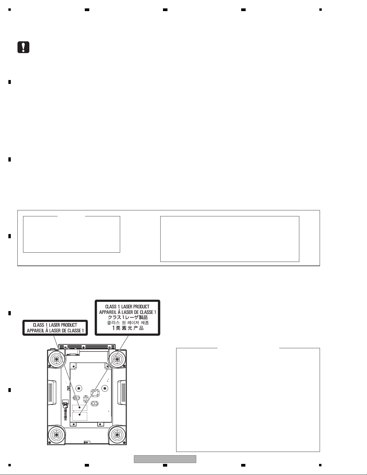
LABEL CHECK
Bottom view
for UXJCB and FLXJ
(Printed on the plate)
for SYXJ8, AXJ5 and KXJ5
(Printed on the plate)
2 3 4
SAFETY INFORMATION
A
B
C
D
E
F
2
1
CDJ-2000NXS
2 3 4

5
6 7 8
CONTENTS
SAFETY INFORMATION.......................................................................................................................................................... 2
1. SERVICE PRECAUTIONS ....................................................................................................................................................5
1.1 NOTES ON SOLDERING............................................................................................................................................... 5
1.2 NOTES ON REPLACING PARTS ................................................................................................................................... 5
1.3 SERVICE NOTICE.......................................................................................................................................................... 6
2. SPECIFICATIONS .................................................................................................................................................................7
3. BASIC ITEMS FOR SERVICE ..............................................................................................................................................7
3.1 JIGS LIST .......................................................................................................................................................................7
3.2 CHECK POINTS AFTER SERVICING ........................................................................................................................... 8
3.3 PCB LOCATIONS ........................................................................................................................................................... 9
4. BLOCK DIAGRAM ..............................................................................................................................................................10
4.1 OVERALL WIRING DIAGRAM .....................................................................................................................................10
4.2 SIGNAL BLOCK DIAGRAM.......................................................................................................................................... 12
4.3 POWER SUPPLY BLOCK DIAGRAM........................................................................................................................... 14
5. DIAGNOSIS ........................................................................................................................................................................ 16
5.1 POWER ON SEQUENCE.............................................................................................................................................16
5.2 FAILURE JUDGEMENT OF THE PICKUP ASSY ........................................................................................................ 17
5.3 TROUBLESHOOTING.................................................................................................................................................. 18
5.4 OPERATIONAL WAVEFORMS .................................................................................................................................... 31
5.5 SETUP SEQUENCE..................................................................................................................................................... 32
5.6 CONNECTION CONFIRMATION WITH THE PC......................................................................................................... 33
6. SERVICE MODE................................................................................................................................................................. 34
6.1 SERVICE MODE .......................................................................................................................................................... 34
6.2 ABOUT THE DEVICE................................................................................................................................................... 51
7. DISASSEMBLY ................................................................................................................................................................... 52
8. EACH SETTING AND ADJUSTMENT................................................................................................................................ 67
8.1 NECESSARY ITEMS TO BE NOTED........................................................................................................................... 67
8.2 FIRMWARE UPDATE / RECOVERY.............................................................................................................................67
8.3 JOG DIAL ROTATION LOAD ADJUSTMENT ............................................................................................................... 68
8.4 TEMPO ZERO POINT ADJUSTMENT.........................................................................................................................69
8.5 ITEMS FOR WHICH
9. EXPLODED VIEWS AND PARTS LIST...............................................................................................................................72
9.1 PACKING SECTION ..................................................................................................................................................... 72
9.2 EXTERIOR SECTION .................................................................................................................................................. 74
9.3 CONTROL PANEL SECTION ....................................................................................................................................... 76
9.4 JOG DIAL SECTION .................................................................................................................................................... 78
9.5 DISPLAY SECTION ...................................................................................................................................................... 80
9.6 SLOT IN MECHA SECTION.........................................................................................................................................82
9.7 TM ASSY-S ................................................................................................................................................................... 84
10. SCHEMATIC DIAGRAM .................................................................................................................................................... 86
10.1 SRVB ASSY (1/2) ....................................................................................................................................................... 86
10.2 SRVB ASSY (2/2), SPCN, INSW and SLMB ASSYS................................................................................................. 88
10.3 MAIN ASSY (1/5)........................................................................................................................................................90
10.4 MAIN ASSY (2/5)........................................................................................................................................................92
10.5 MAIN ASSY (3/5)........................................................................................................................................................94
10.6 MAIN ASSY (4/5)........................................................................................................................................................96
10.7 MAIN ASSY (5/5)........................................................................................................................................................98
10.8 JACB ASSY .............................................................................................................................................................. 100
10.9 SDCB ASSY .............................................................................................................................................................102
10.10 USBB ASSY ...........................................................................................................................................................104
10.11 TFTB ASSY (1/2)....................................................................................................................................................106
10.12 TFTB ASSY (2/2)....................................................................................................................................................108
10.13 PNLB ASS
Y............................................................................................................................................................110
10.14 JFLB ASSY............................................................................................................................................................. 112
10.15 CDCB and SDSW ASSYS......................................................................................................................................114
10.16 SLDB and EUPB ASSYS........................................................................................................................................115
10.17 CNCT and KSWB ASSYS ......................................................................................................................................116
10.18 JOGB and INDB ASSYS ........................................................................................................................................ 117
10.19 POWER SUPPLY and ACIN ASSYS ...................................................................................................................... 118
10.20 WAVEFORMS.........................................................................................................................................................120
USER SETTINGS ARE AVAILABLE........................................................................................... 70
A
B
C
D
E
F
CDJ-2000NXS
5
6 7 8
3

1
2 3 4
11. PCB CONNECTION DIAGRAM ......................................................................................................................................122
11.1 SRVB ASSY..............................................................................................................................................................122
A
11.2 SPCN, INSW and SLMB ASSYS..............................................................................................................................127
11.3 MAIN ASSY...............................................................................................................................................................128
11.4 JACB, SDCB and USBB ASSYS ..............................................................................................................................132
11.5 TFTB ASSY...............................................................................................................................................................134
11.6 PNLB ASSY ..............................................................................................................................................................138
11.7 JFLB, CDCB and SDSW ASSYS..............................................................................................................................142
11.8 SLDB, EUPB and CNCT ASSYS ..............................................................................................................................146
11.9 KSWB, JOGB and INDB ASSYS ..............................................................................................................................148
11.10 POWER SUPPLY and ACIN ASSYS.......................................................................................................................150
12. PCB PARTS LIST ............................................................................................................................................................152
B
C
D
E
F
4
1
2 3 4
CDJ-2000NXS
5
• For environmental protection, lead-free solder is used on the printed circuit boards mounted in this unit.
Be sure to use lead-free solder and a soldering iron that can meet specifications for use with lead-free solders for repairs
accompanied by reworking of soldering.
• Compared with conventional eutectic solders, lead-free solders have higher melting points, by approximately 40 ºC.
Therefore, for lead-free soldering, the tip temperature of a soldering iron must be set to around 373 ºC in general, although
the temperature depends on the heat capacity of the PC board on which reworking is required and the weight of the tip of
the soldering iron.
Do NOT use a soldering iron whose tip temperature cannot be controlled.
Compared with eutectic solders, lead-free solders have higher bond strengths but slower wetting times and higher melting
temperatures (hard to melt/easy to harden).
The following lead-free solders are available as service parts:
• Parts numbers of lead-free solder:
GYP1006 1.0 in dia.
GYP1007 0.6 in dia.
GYP1008 0.3 in dia.
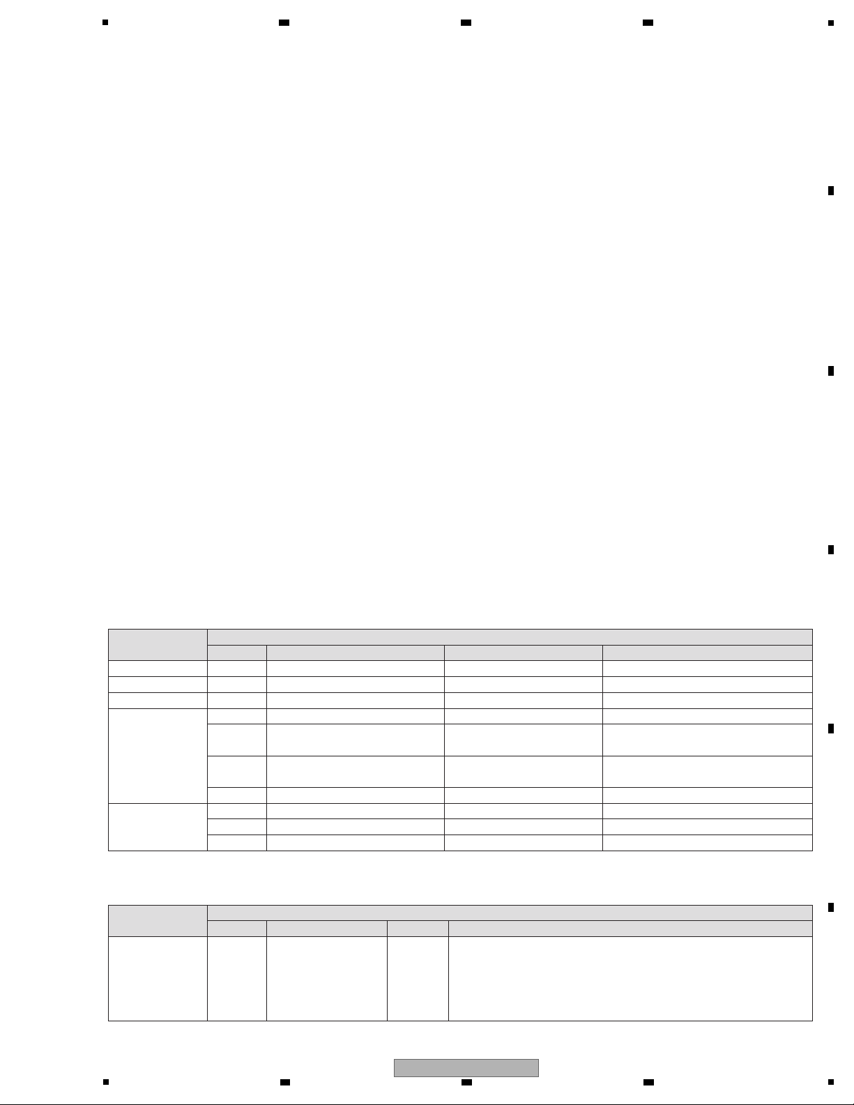
The part listed below is difficult to replace as a discrete component part.
When the part listed in the table is defective, replace whole Assy.
Assy Name
CDCB Assy
CDC SENSOR AD7147ACPZ500RL7
IC with heat-pad
IC5001
SRVB Assy 12V→USB5V DC/DC converter BD9328EFJ
IC with heat-pad
IC7301
12V→3.3V DC/DC converter BD9328EFJ
IC with heat-pad
IC7302
12V→5V DC/DC converter BD9328EFJ
IC with heat-pad
IC7305
TFTB Assy BACK LIGHT CONTROL TK61222CQ6
IC with heat-pad
IC4018
USBB Assy USB CURRENT LIMIT IC TPS2557DRB
IC with heat-pad
IC6301
12V→1.2V DC/DC converter BD9328EFJ IC with heat-padIC705
MAIN Assy
CPU R5S77641N300BG
BGA package
IC10
Authentication Coprocessor 337S3959-TBB USON package
(UltraSmallOutlineNon-lead)
IC14
DSP D810K013BZKB400
D810K013CZKB400
BGA packageIC301
Parts that is Difficult to Replace
Ref No. Function Part No. Remarks
The part listed below is difficult to replace as a discrete component part.
The replaceing method see remarks.
Assy Name
JFLB Assy
JOG FL DEL1058
As the JOG FL is integrated with the FL Holder (DNF1735) with the aid of two
pieces of double-back tape (Z12-016), first remove the integrated JOG FL and
FL Holder, attach a new JOG FL and an FL Holder, using two pieces of
double-back tape, then mount them together. (Note: As the integrated JOG FL
and FL Holder are exactly the same parts as those for the CDJ-2000, you can
handle them in the same manner as with the CDJ-2000.)
V9201
Parts that is Difficult to Replace
Ref No. Function Part No. Remarks
6 7 8
1. SERVICE PRECAUTIONS
1.1 NOTES ON SOLDERING
A
B
1.2 NOTES ON REPLACING PARTS
5
6 7 8
CDJ-2000NXS
C
D
E
F
5

1
About the PNLB and CNCT Assys
The PNLB Assy and CNCT Assy are wired with jumper leads. The PNLB Assy (Part No. DWX3338) is supplied as a service
part with the CNCT Assy connected. The CNCT Assy is not supplied individually as a service part.
About the Flash ROM (IC3) in the MAIN Assy
Replacement of the Flash ROM (IC3: DYW1814) in the MAIN Assy is not possible during service, because writing of
the MAC address on the production line is required.
Therefore, the Flash ROM (IC3) is not supplied as a service part. If the Flash ROM is defective, replace the whole MAIN Assy.
About work required after replacement of the Traverse Mechanism Assy (09SD)
After replacement of the traverse mechanism Assy (09SD), reset the LD lighting time to zero.
How to Reset: See "7 Drive LD life reset" in "[3] Indication of various information" in "6.1 SERVICE MODE."
About transfer of the accumulated LD lighting time data after replacement of the MAIN Assy
This unit is equipped with self-diagnostic functions for the drives in Service mode. The service-life check for the laser
diode (for CDs/DVDs) among the self-diagnostic functions uses the accumulated lighting time for judgment. If it is
7,000 hours or less, the laser diode is judged as OK. The accumulated lighting time of the LD is stored in the Flash ROM
(IC3: DYW1814) in the MAIN Assy. Therefore, after replacement of the MAIN Assy, the accumulated lighting time of the
LD is cleared and proper judgment will not be possible after that. To avoid such a situation, when replacement of the
MAIN Assy is required, transfer the LD accumulated lighting time data.
Before replacement, confirm the drive LD lighting time in Service mode and take note of the time value. After replacement
is finished, enter Service mode then change the drive LD lighting time value to what you noted.
For details on how to confirm and change the LD lighting time, see "8 Drive LD life manual input" in "[3] Indication of
various information" in "6.1 SERVICE MODE."
About the self-diagnostic functions for the drives
This unit has self-diagnostic functions for the drives in Service mode. Use the self-diagnostic functions to check the drives if
the problem symptom pointed out by the customer is a malfunction related to the drives or if a drive-related error is logged in
the error history.
For details on the self-diagnostic functions for the drives, see "[5] Drive Self-Diagnosis" and "[6] Contents of Drive
Self-Diagnosis" in "6.1 SERVICE MODE."
About the iPod cable supplied with this unit
An iPod cable is supplied with this unit. Be sure to use the iPod cable supplied with this unit to connect an iPad with this unit in
order to determine the cause of a charging problem with an iPad. Do not use the standard cable supplied with iPhones for this
purpose, because it does not meet the specifications required for iPads (a voltage drop may result, because it is thin).
The iPod cable supplied with this unit has been registered as service jig.
About backup of the UTILITY settings
As this unit is provided with user-settable UTILITY settings (such as the Play mode setting,) it is recommended that you back
up the settings before starting repair. The settings can be stored for backup in a USB memory device or an SD card.
For details on how to back up and restore data, see "g How to Back Up and Restore the Settings" in "8.5 ITEMS
FOR WHICH USER SETTINGS ARE AVAILABLE ."
2 3 4
1.3 SERVICE NOTICE
A
B
C
D
E
F
6
1
2 3 4
CDJ-2000NXS
5
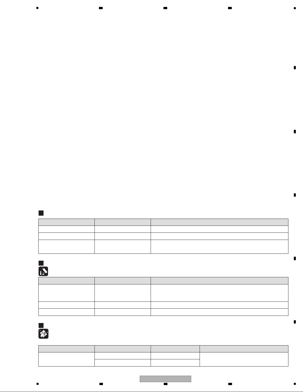
Power consumption..................................................................37 W
Power consumption (standby) ................................................0.4 W
Main unit weight...................................................................... 4.7 kg
External dimensions .......320 mm (W) × 106.5 mm (H) × 405.7 mm (D)
Tolerable operating temperature.............................. +5 °C to +35 °C
Tolerable operating humidity............5 % to 85 % (no condensation)
Analog audio output (AUDIO OUT L/R)
Output terminals ..........................................................RCA terminal
Digital audio output (DIGITAL OUT)
Output terminals ..........................................................RCA terminal
Output type..................................................Coaxial digital (S/PDIF)
USB downstream section (USB)
Port........................................................................................ Type A
Power supply..........................................................5 V/2.1 A or less
USB upstream section (USB)
Port........................................................................................ Type B
LAN (PRO DJ LINK)
Rating ........................................................................... 100Base-TX
Control output (CONTROL)
Port..................................................................................... Mini-jack
SD memory card section
File system ....Conforming to “SD Specifications Part 2 File System
Specification Version 2.00”
Max. memory capacity............................................................32 GB
Main display
Display type.............. Active matrix TFT liquid crystal display (LCD)
Screen size................................................................. 6.1-inch, wide
Supported languages ................................................. 18 languages
• The specifications and design of this product are subject to
change without notice.
Cleaning
Name Part No. Remarks
Cleaning paper GED-008
Cleaning liquied GEM1004 Refer to "9.7 TM ASSY-S".
Position to be cleaned
Pickup lens
Before shipping out the product, be sure to clean the following positions by using the prescribed cleaning tools.
Name Part No. Remarks
Lubricating oil GYA1001 Refer to “9.3 CONTROL PANEL SECTION”,
“9.4 JOG DIAL SECTION”, “9.6 SLOTIN MECHA
SECTION”, “9.7 TM ASSY-S”.
Dyfree GEM1036 Refer to “9.6 SLOTIN MECHA SECTION”.
Lubricating oil GEM1034 Refer to “9.4 JOG DIAL SECTION”.
Lubricants and Glues List
Jigs List
Jig Name Part No. Purpose of use / Remarks
CD test disc STD-905 Drive self-diagnosis
DVD test disc GGV1035 (DVDT-001) Drive self-diagnosis
iPod cable GGP1201
For use in determining a cause of charging problem for an iPad
DDE1142 (accessory for the CDJ-2000NXS) registered as a special tool
2. SPECIFICATIONS
6 7 8
A
B
3. BASIC ITEMS FOR SERVICE
3.1 JIGS LIST
C
D
E
CDJ-2000NXS
5
6 7 8
F
7
1
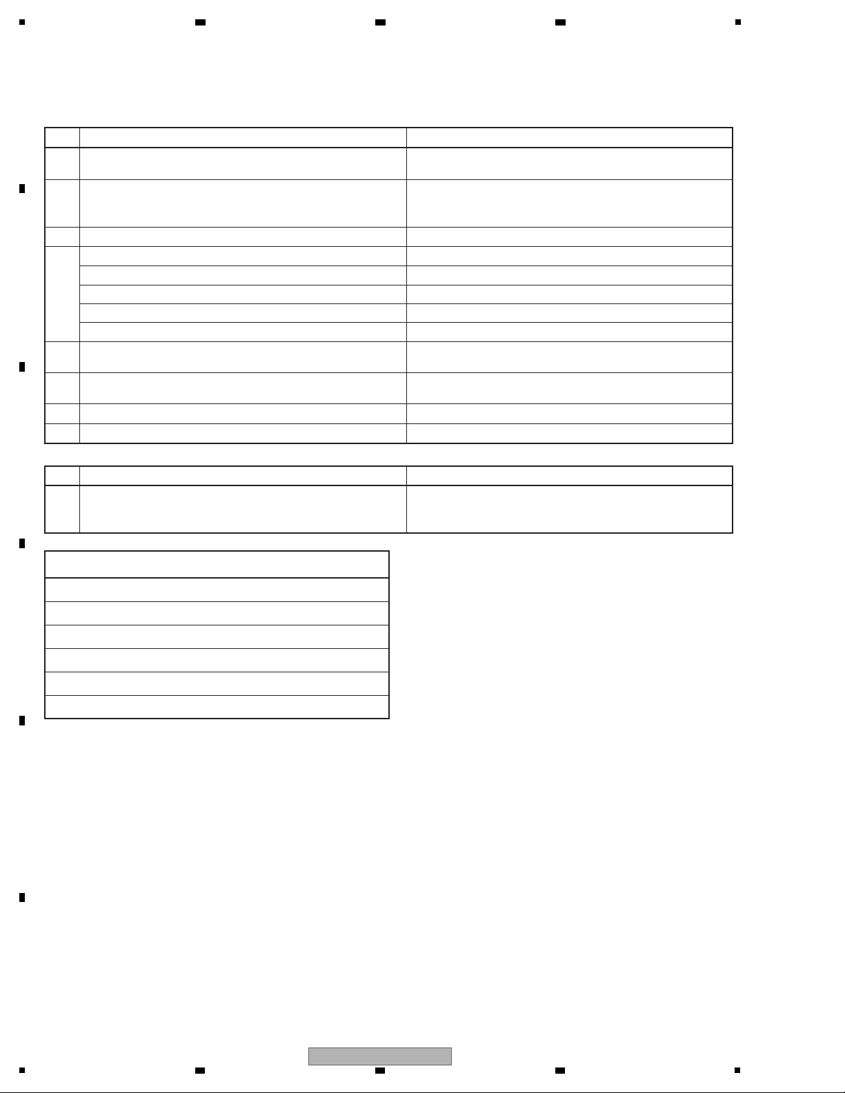
No. Check pointsProcedure
1
Confirm the firmware version on Service Mode.
The version of the firmware must be latest.
Update firmware to the latest one, if it is not the latest.
2
Confirm whether the customer complain has been solved.
If the customer complain occurs with the specific disc, use it for
the operation check.
The customer complain must not be reappeared.
Audio and operations must be normal.
Playback data contained in the device connected to USB A.
Audio, Search and operations must be normal.
USB B
The PC must be linked.
Playback data contained in an SD card.
Audio, Search and operations must be normal.
LINK
The PC must be linked.
3 Playback a disc. (track search) Audio, Search and operations must be normal.
5 Check output signals while the JOG dial or TEMPO slider is
being operated.
Audio and operations must be normal.
6 Check the keys on the unit. Check whether a product can be operated properly by buttons
on the product.
7 Check the LCD display.
Check that there is no dirt or dust trapped inside the LCD display.
4 Check the connection of each interface.
Items to be checked after servicing
No. Check pointsProcedure
1
Confirm playback error rates at the innermost and outermost
tracks by using the following disc.
DVD test disc (GGV1025)
The error rates must be less than 5.0e-4.
(This procedure can determine if the drive is degraded.)
Specific Items to be Checked
To keep the product quality after servicing, confirm recommended check points shown below.
8
Check the appearance of the product.
No scratches or dirt on its appearance after receiving it for service.
Item to be checked regarding audio
Distortion
Noise
Volume too low
Volume too high
Volume fluctuating
Sound interrupted
See the table below for the items to be checked regarding audio.
2 3 4
3.2 CHECK POINTS AFTER SERVICING
A
B
C
D
E
F
8
1
2 3 4
CDJ-2000NXS
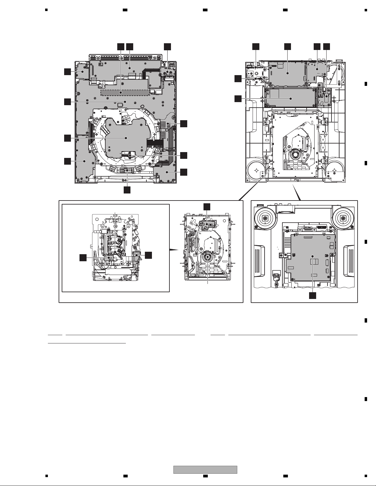
5
F
JACB
ASSY
D
SLMB ASSY
TM ASSY 09SD-S
A
SRVB ASSY
S
INDB ASSY
E
MAIN
ASSY
U
ACIN ASSY
H
USBB ASSY
I
TFTB ASSYMSDSW ASSY
L
CDCB ASSY
Q
KSWB ASSY
B
SPCN
ASSY
P
CNCT ASSY
R
JOGB ASSY
T
POWER SUPPLY
ASSY
G
SDCB ASSY
SLOTIN MECHA
G11 ASSY
• Bottom view
• Bottom view
• Bottom view
O
EUPB
ASSY
N
SLDB
ASSY
C
INSW
ASSY
J
PNLB
ASSY
K
JFLB
ASSY
1..MAIN ASSY DWX3312
NSP 1..TFTA ASSY DWM2458
2..TFTB ASSY DWX3331
2..CDCB ASSY DWX3332
2..SDCB ASSY DWX3333
NSP 1..SRVA ASSY DWM2459
2..SRVB ASSY DWX3334
2..INSW ASSY DWX3335
2..SPCN ASSY DWX3336
2..INDB ASSY DWX3337
NSP 1..PNLA ASSY DWM2460
2..PNLB ASSY DWX3338
2..KSWB ASSY DWX3339
2..SDSW ASSY DWX3340
2..EUPB ASSY DWX3341
2..SLDB ASSY DWX3342
NSP 2..CNCT ASSY DWX3343
NSP 1..JFLA ASSY DWM2461
2..SLMB ASSY DWX3345
2..ACIN ASSY DWX3346
2..JFLB ASSY DWX3348
2..JOGB ASSY DWX3349
2..JACB ASSY DWX3350
1..USBB ASSY DWX3395
> 1..POWER SUPPLY ASSY DWR1463
NSP SLOTIN MECHA G11 ASSY DXA2163
TM ASSY 09SD -S DXX2697
Mark No. Description Part No. Mark No. Description Part No.
LIST OF ASSEMBLIES
NOTES: - Parts marked by “NSP” are generally unavailable because they are not in our Master Spare Parts List.
-
The > mark found on some component parts indicates the importance of the safety factor of the part.
Therefore, when replacing, be sure to use parts of identical designation.
3.3 PCB LOCATIONS
6 7 8
A
B
C
5
CDJ-2000NXS
6 7 8
D
E
F
9
1
!
!
!
!!
V+3R3
SD_DET
SD_CMD
SD_DATA3
SD_DATA1
SD_DATA2
SD_DATA0
SD_CLK
SD_WP
GNDD
GNDD
A_S2
V+5A
7/x6
A_C
A_D
A_S1
GNDD
A_A
VR65
VR78
A_B
VRCOM
RF
LD78
F+
T-
LD65
T+
PD
F-
GNDSD
INSW
GNDSD
GNDD
STBY_CTRL_IN
NC
GNDD
V+12_EUP
CPU_EUP_CONT
EUP_CONT
USB_STOP
USB_LED
PNL_CNVSS
PNL_SCK
PNL_BUSY
PNL_TXD
PNL_RXD
PNL_RST
V+12
V+12
V+5
V+3R3
V+3R3
V+1R2
TFT_DATA0
TFT_DATA1
TFT_TFS1
TFT_TSCLK1
TFT_RSCLK1
TFT_RST
GNDD
TFT_PF1
GNDD
GNDD
TFT_DATA3
TFT_RFS1
GNDD
USB_DP_A
USB_DN_A
GNDD
GNDD
VBUS_B
USB_DN_B
USB_DP_B
GNDD
GNDD
HSSW_PWREN
HSSW_PWRFL
GNDD
VREF1
V+12_SWITCHED_IN
V+12_SWITCHED_IN
V+12_STBY10mA
RKP1751-A
1
2
B6B-XH-A
1
2
345
6
AKM1283-A
1
2
3
4
5
6
7
8
9
10
11
12
KM200NA3
V+5_USB_D
1
V+5_USB_D
2
GNDD
3
KM200NA5L
1
2
3
4
5
DKN1288-A
ST1+
1
ST1-
2
ST2+
3
ST2-
4
1
2
3
4
52151-0510
1
2
3
4
5
52147-0510
1
2
3
4
5
AKM1291-A
LO-
1
LO+
2
GNDSD
3
LPS1
4
LPS2
5
VKN 1414-A
1
2
3
4
5
6
7
8
9
10
NM
V+3.3V
1
BF_EMU#
2
GNDD
3
BF_TMS
4
BF_TCK
5
BF_TRST#
6
BF_TDI
7
BF_TDO
8
GNDD
9
GNDD
10
CKS5561-B
NC
1
CATHODE2
2
CATHODE1
3
NC
4
NC
5
ANODE2
6
ANODE1
7
NC
8
NC
9
NC
10
VKN 1414-A
1
2
3
4
5
6
7
8
9
10
AKM1298-A
V+12_EUP
1
V+12
2
V+12
3
XEUP_CONT
4
GNDD
5
GNDD
6
V+5
7
GNDD
8
V+3R3
9
V+3R3
10
GNDD
11
GNDD
12
DKN1205-A
1
2
3
4
5
6
7
8
9
10
11
12
DKN1312-A
NC
1
W
2
V
3
U
4
HB
5
HW-
6
HW+
7
HV-
8
HV+
9
HU-
10
HU+
11
V+5
12
VKN 1417-A
123456789
101112
13
VKN 1273-A
123456789
101112
13
DKN1313-A
V+5
1
HU+
2
HU-
3
HV+
4
HV-
5
HW+
6
HW-
7
HB
8
U
9
V
10
W
11
GNDSD
12
INSW
13
DKN1313-A
1
2
3
4
5
6
7
8
9
10
11
12
13
VKN 1273-A
123456789
101112
13
RKN1054-A
V-12
1
GNDD
2
V+12
3
GNDD
4
SPDIF
5
CONT2
6
V+5_DAC
7
CONT1
8
MUTE
9
A_LOUT
10
GNDA
11
A_ROUT
12
GNDA
13
DKN1445-A
1
2
3
4
5
6
7
8
9
10
11
12
13
14
15
16
17
18
19
20
21
22
23
241
2
3
4
5
6
7
8
9
10
11
12
13
14
15
16
17
18
19
20
21
22
23
24
NM
V+3R3_CPU
1
V+3R3_CPU
2
GNDD
3
GNDD
4
NC
5
CPU_TRST
6
CPU_TDI
7
CPU_TMS
8
CPU_TCK
9
CPU_TDO
10
CPU_MPMD
11
CPU_AUDSYNC
12
CPU_AUDATA3
13
CPU_AUDATA1
14
CPU_AUDATA0
15
CPU_EMU_BRK
16
CPU_RST
17
GNDD
18
DSP_TMS
19
DSP_TDI
20
DSP_TDO
21
DSP_TCK
22
DSP_EMU0
23
DSP_TRST
24
VKN 1433-A
1
2
3
4
5
6
7
8
9
10
11
12
13
14
15
16
17
18
19
20
21
22
23
24
25
26
27
28
29
VKN 1433-A
1
2
3
4
5
6
7
8
9
10
11
12
13
14
15
16
17
18
19
20
21
22
23
24
25
26
27
28
29
CKS5660-A
GND
1
GND
2
GND
3
NC
4
VCC
5
VCC
6
VCC
7
VCC
8
NC
9
TEST3
10
TEST2
11
TEST1
12
VSYNC
13
HSYNC
14
GND
15
SHUT
16
GND
17
R5
18
R4
19
R3
20
R2
21
R1
22
R0
23
GND
24
G5
25
G4
26
G3
27
G2
28
G1
29
G0
30
GND
31
B5
32
B4
33
B3
34
B2
35
B1
36
B0
37
GND
38
DCLK
39
GND
40
VKN 2050-A
ATA_RST
1
GNDD
2
ATA_D7
3
ATA_D8
4
ATA_D6
5
ATA_D9
6
ATA_D5
7
ATA_D10
8
ATA_D4
9
ATA_D11
10
ATA_D3
11
ATA_D12
12
ATA_D2
13
ATA_D13
14
ATA_D1
15
ATA_D14
16
ATA_D0
17
ATA_D15
18
GNDD
19
GNDD
20
ATA_DREQ
21
GNDD
22
ATA_WR
23
GNDD
24
ATA_DIOR
25
GNDD
26
ATA_RDY
27
GNDD
28
ATA_DACK
29
GNDD
30
ATA_INT
31
GNDD
32
ATA_A1
33
GNDD
34
ATA_A0
35
ATA_A2
36
GNDD
37
ATA_CA0
38
ATA_CS1
39
GNDD
40
FH12-40S-0.5SH(55)
1
2
3
4
5
6
7
8
9
10
11
12
13
14
15
16
17
18
19
20
21
22
23
24
25
26
27
28
29
30
31
32
33
34
35
36
37
38
39
40
VKN 181 8-A
1
2
3
4
5
6
7
8
9
10
11
12
13
14
15
16
17
18
19
20
21
22
23
24
25
26
27
28
29
30
31
32
33
34
35
36
37
38
39
40
1
SD
2
SD
3
GN
4
VD
5
SD
6
GN
7
SD
8
SD
10
SD
9
SD
B2P3-VH
1
2
VKN 1940-A
1
2
VKN 1940-A
1
2
AKM1289-A
1
2
3
DKN1599-A
1
2
345
6
DKB1113-A
2
1
RKN1004-A
231
DKB1102-A
432
1
DKB1106-A
1
2
3
4
RT1
RT2
DKN1646-A
1
2
3
4
RT1
RT2
DSA1037-A
S9101
12
ZWNN1007G28-9-07A
L=70mm
WHITE SINGLE WIRE
LO+
ZWNN1007G28-8 -07A
L=70mm
GRAY SINGLE WIRE
LOADING MOTOR
LO-
DKP3822-A
L=55mm
LIVE
NEUTRAL
PURPLE
BLUE
LR
AUDIO OUT
CONTROL OUT
DIGITAL OUT
FOR DEBUG (BF)
09SD PICK UP ASSY
STEPPING
MOTOR SK
DC MOTOR
TM ASSY 09SD-S (DXX2697)
SPINDLE MOTOR G11
USB CONNECTOR
(A TYPE)
ETHERNET
CONNECTOR
TFT-LCD MODULE (CWX3970-)
LO+
LO-
DKN1650-A
FOR DEBUG (DSP&CPU)
DDD1481
L=258mm
DDD1480
L=78mm
FFC(SAME FACE)
D20PDY0
DDD1484
L=78mm
DDD1479
L=68mm
DKP3845
L=50mm
CONNECTOR ASSY
DKP3844
L=90mm
PF05PP-C25
L=250mm
DDD1460
L=98mm
DKP3769
L=180mm
DDD1452
L=78mm
*RIGHT ANGLE
*RIGHT ANGLE
FRAME
GND
CHASSIS
GND
DE007VE0
L=70mm
DDD1541
L=58mm
FFC(SAME FACE)
GOLD PLATING
FFC(SAME FACE)
FFC(SAME FACE)
CONNECTOR ASSY
CONNECTOR ASSY
EARTH LEAD UNIT
CONNECTOR ASSY
FFC(SAME FACE)
FFC(SAME FACE)
Vertical
Horizontal
Vertical
USB CONNECTOR
(B TYPE)
*VERTICAL
Vertical
Horizontal
Vertical
Horizontal
Horizontal
Horizontal
Horizontal
Horizontal
Vertical
Vertical
Vertical
Horizontal
Horizontal
Vertical
FFC(REVERSE)
DDD1606
L=67mm
Horizontal
Horizontal
Horizontal
Horizontal
Horizontal
Horizontal
JP9101
Vertical
DKP3935
DKP3934
DKP3939
L=167mm
CRIMP
CONNECTOR
CONNECTOR ASSY
FFC
SAME FACE
DESTINATION
/SYXJ8
/FLXJ
/AXJ5
/KXJ5
/UXJCB
DKP3935DKP3935-
DKP3935DKP3935DKP3934-
AC INLET AC POWER CORD
XDG3061ADG7076-(Taiwan)
ADG7105ADG7115DDG1108-
XDG3061-
CN 9101
CN 2
CN 705
CN 6302
CN 9001
CN 7004
CN8601
CN8651
CN 7003
CN 5102
CN 4001
CN 4014
CN 702
CN 7301
CN8055
CN 6102
CN 703
CN 9401
CN 7009CN 6101
CN 6301
CN 501
CN 7001
CN 1
CN 502
CN 704 CN4002
CN 4013
CN 701
CN 7005
CN 1
CN 6001
CN 6103
CN 7303
CN 7302
JA9403
JA9401
JA9402
JA6301
JA6302
JA702
EARTH
NEUTRAL(Blue) 98+/-3mm
LIVE(Brown) 112+/-3mm
EARTH
(Green&Yellow Stripe)
63+/-3mm
CHASSIS
NEUTRAL
LIVE
NEUTRAL
LIVE
LIVE
NEUTRAL
NEUTRAL
LIVE(Brown) 114+/-3mm
NEUTRAL(Blue) 100+/-3mm
LIVE
NEUTRAL
LIVE
AC POWER CORD AC INLET
Backlight Module
F
JACB ASSY
(DWX3350)
O
EUPB ASSY
(DWX3341)
TFTB ASSY (DWX33
I
I I
1/2, 2/2
E
E E
1/5- 5/5
MAIN ASSY (DWX3312)
SRVB ASSY (DWX3334)
A
A A
1/2, 2/2
SLOTIN MECHA G11 ASSY
D
C
SLMB ASSY
(DWX3345)
INSW ASSY
(DWX3335)
B
SPCN ASSY
(DWX3336)
T
POWER SUPPLY
ASSY (DWR1463)
!
U
ACIN ASSY
(DWX3346)
H
USBB ASSY
(DWX3395)
M
SDSW ASSY
(DWX3340)
G
SD
(D
2 3 4
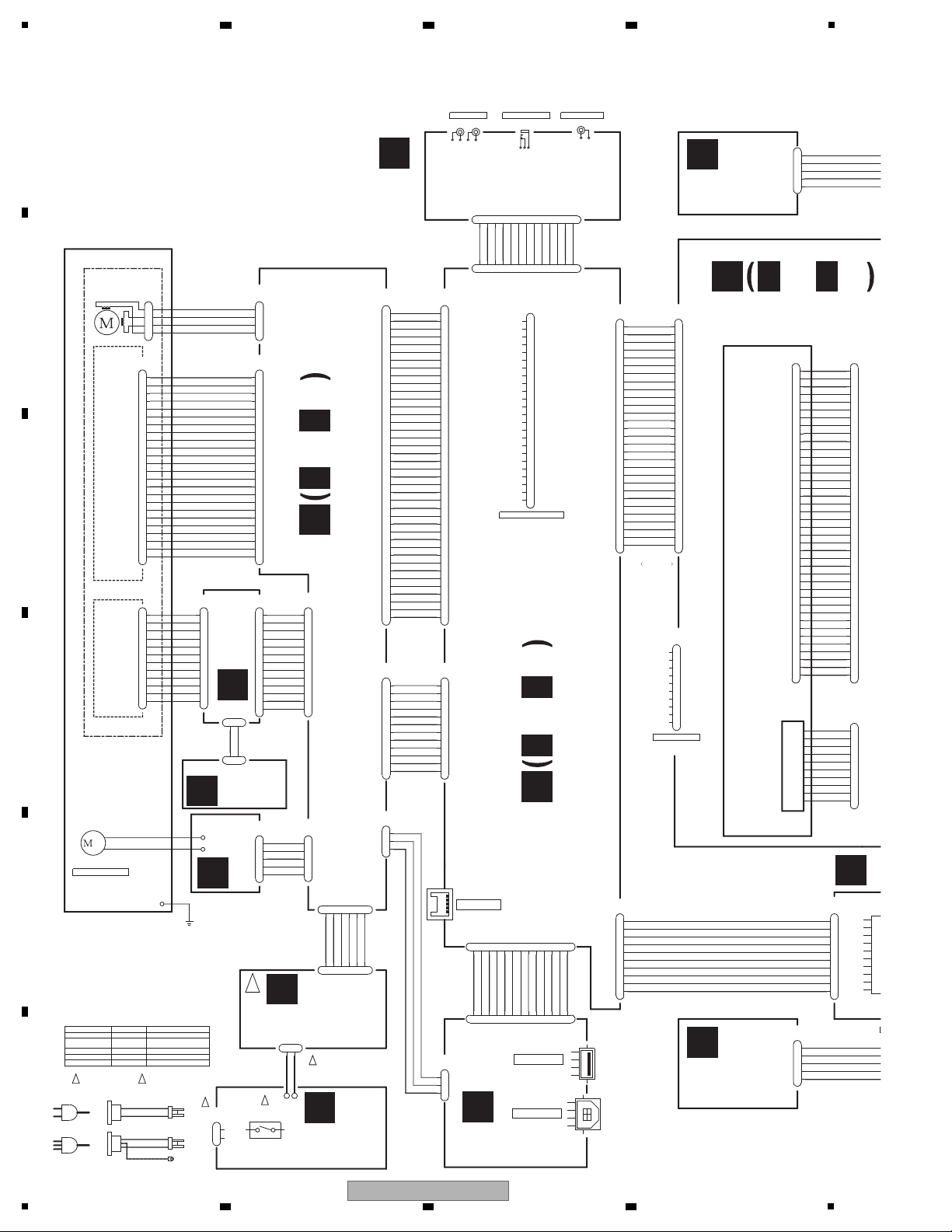
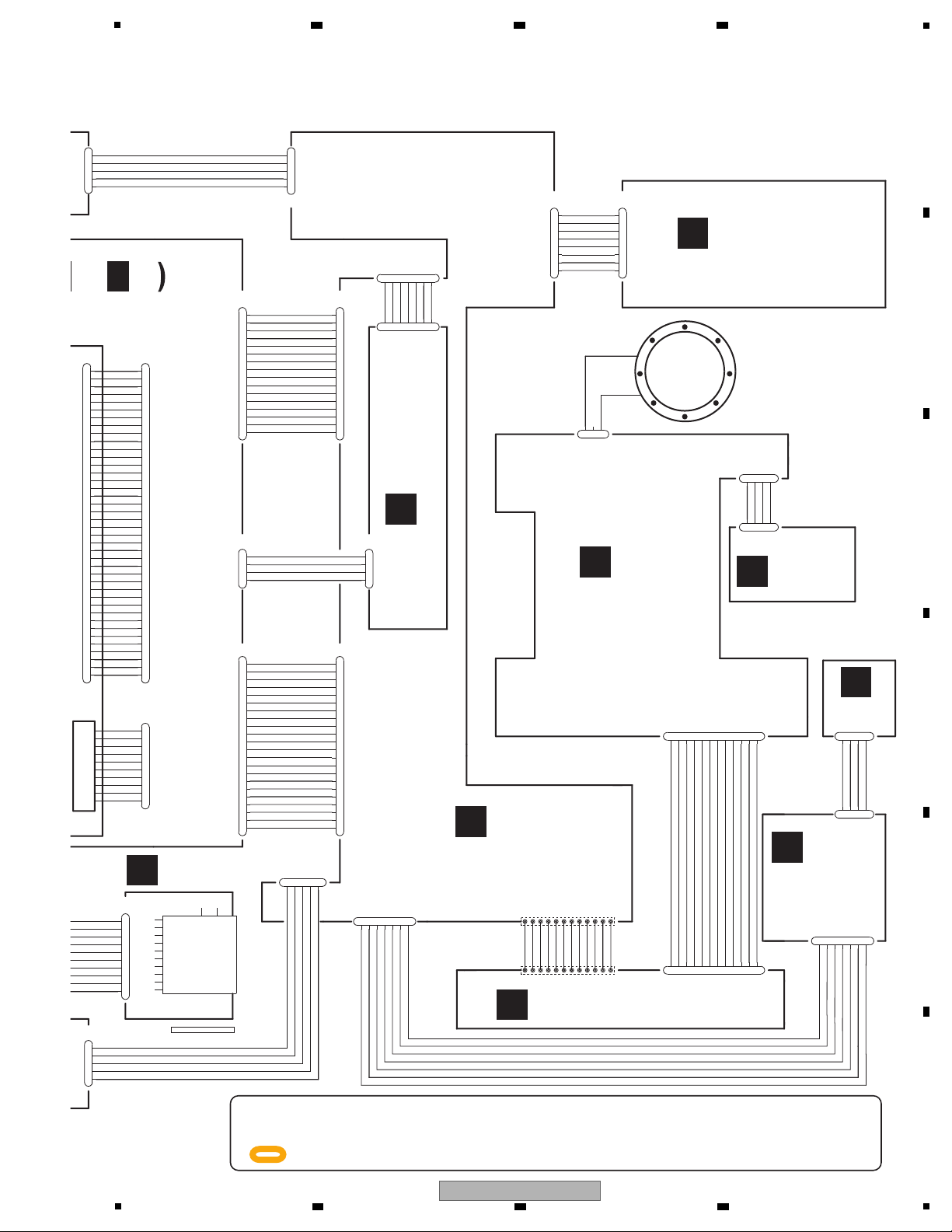
4. BLOCK DIAGRAM
4.1 OVERALL WIRING DIAGRAM
A
B
C
D
E
F
10
1
2 3 4
CDJ-2000NXS
5
V+3R3
JOG1
JOG2
GNDD
V+12
GNDD
V+3R3
JOGILM_R
JOGILM_W
J_LAT
J_DSO
J_BK
J_SCLK
JOG2
JOG1
JOG_SW
KEY3_B
TRSTL
GNDD
ADCT
ADIN
V+3R3E
GNDS
V+5
USB_LED
USB_LED
USB_STOP
USB_STOP
SD_SW
SD_SW
EUPL
EJECTL
KEY4_B
V+5
V+5
GNDD
GNDD
PRPRL
S_SDL
INFOL
S_LINKL
BRWSL
S_USBL
MENUL
KEY2
V+3R3
USB_STOP
V+5
KEY1
GNDD
USB_LED
GNDD
V+12
V+12
V+12EUP
GNDD
GNDD
V+5
PNL_BUSY
ENC_2
PNL_SCK
ENC_1
PNL_TXD
PNL_RST
PNL_RXD
PNL_CNVSS
CPU_EUP_CONT
ENC_SW
EUP_CON
ENCL
JOG2
JOG1
V+3R3
J_DSO
J_BK
J_LAT
JOG_SW
J_SCLK
GNDD
JOGILM_R
JOGILM_W
V+12
V+3R3
GNDD
CDC_INT
CDC_DSO
CDC_DSI
CDC_SCLK
CDC_CS
S_DISKL
R_BOXL
QUANTIZEL
KEY0
NEEDLEL
V+12
GNDD
GNDD
D_INDIL
V+12
V+12
GND_LED
NEEDLEL
GNDD
V+5
D_INDL
D_INDL
D_INDL
PLAY
PLAY
PLAY
CUE
CUE
CUE
PLAYL
PLAYL
PLAYL
CUEL
CUEL
CUEL
GNDD
GNDD
GNDD
V+12
V+12
V+12
CKS1072-A
JOG_SW
1
NC
2
GNDD
3
VKN 1409-A
1
2
3
4
RKN1045-A
1
2
3
4
52151-0410
1
2
3
4
VKN 1264-A
1
2
3
4
VKN 1409-A
1
2
3
4
52151-0510
1
2
3
4
5
1
2
3
4
5
VKN 1267-A
1234567
VKN 1411-A
1234567
52147-0710
1234567
VKN 1414-A
1
2
3
4
5
6
7
8
9
10
CKS5561-B
NC
1
CATHODE2
2
CATHODE1
3
NC
4
NC
5
ANODE2
6
ANODE1
7
NC
8
NC
9
NC
10
52147-1210
1
2345678
9
101112
VKN 1276-A
1
2
3
4
5
6
7
8
9
10
11
12
13
14
15
16
VKN 1420-A
1
2
3
4
5
6
7
8
9
10
11
12
13
14
15
16
VKN 1426-A
1
2
3
4
5
6
7
8
9
10
11
12
13
14
15
16
17
18
19
20
21
22
VKN 1282-A
1
2
3
4
5
6
7
8
9
10
11
12
13
14
15
16
17
18
19
20
21
22
CKS5660-A
GND
1
GND
2
GND
3
NC
4
VCC
5
VCC
6
VCC
7
VCC
8
NC
9
TEST3
10
TEST2
11
TEST1
12
VSYNC
13
HSYNC
14
GND
15
SHUT
16
GND
17
R5
18
R4
19
R3
20
R2
21
R1
22
R0
23
GND
24
G5
25
G4
26
G3
27
G2
28
G1
29
G0
30
GND
31
B5
32
B4
33
B3
34
B2
35
B1
36
B0
37
GND
38
DCLK
39
GND
40
1
2
3
4
5
6
7
8
9
10
11
12
13
14
15
16
17
18
19
20
21
22
23
24
25
26
27
28
29
30
31
32
33
34
35
36
37
38
39
40
CKS5956-A
1
SD_DATA3
2
SD_CMD
3
GND
4
VDD
5
SD_CL
6
GND2
7
SD_DATA0
8
SD_DATA1
10
SD_DET
9
SD_DATA2
12
SD_W
11
TER
51048-0400
123
4
51048-0500
12345
51048-0500
1
2
3
4
5
51048-0700
1234567
51048-0800
1
2
3
4
5
6
7
8
51048-0800
1
2
3
4
5
6
7
8
51048-1200
123456789
101112
SD CARD CONNECTOR
SHEET SW
(DSX1078-)
DDD1609
L=60mm
D20PDY0505E
L=50mm
D20PDY0510E
L=100mm
D20PDD0810E
L=100mm
PARALLEL JUMPER
DDD1611
L=210mm
D20PYY0405E
L=50mm
JUMPER
L=22.5mm
D20PDY1210E
L=100mm
DDD1483
L=68mm
DDD1485
L=108mm
DDD1541
L=58mm
FFC(SAME FACE)
GOLD PLATING
PARALLEL JUMPER
PARALLEL JUMPER
PARALLEL JUMPER
PARALLEL JUMPER
FFC(SAME FACE)
FFC(SAME FACE)
FFC(SAME FACE)
PARALLEL JUMPER
Horizontal
Horizontal
Vertical
Horizontal
Vertical
Horizontal
Vertical
Vertical
DDD1607
L=115mm
FFC(SAME FACE)
JP8002
JP8001
JP8003
JP8004
Horizontal
Horizontal
DDD1608
L=75mm
FFC(SAME FACE)
JP9203
JP9202
Horizontal
Vertical
Horizontal
Vertical
CN 9203
CN 4015
CN 6201
CN 9301
CN8501
CN 5002
CN8601
CN8003
CN 5001
CN8502
CN 5102
CN 4014
CN8801
CN8002CN 4007
CN 4012
CN8001
CN 4013
CN 5101
JH9202
JH8001
JH8002
JH8004
JH8701
JH8003
JH9201
Backlight Module
I
1/2, 2/2
G
SDCB ASSY
(DWX3333)
J
PNLB ASSY
(DWX3338)
P
CNCT ASSY (DWX3343)
Q
KSWB ASSY
(DWX3339)
K
JFLB ASSY
(DWX3348)
S
INDB ASSY
(DWX3337)
R
JOGB ASSY
(DWX3349)
L
CDCB ASSY
(DWX3332)
N
SLDB ASSY
(DWX3342)
-
When ordering service parts, be sure to refer to "EXPLODED VIEWS and PARTS LIST" or "PCB PARTS LIST".
-
The > mark found on some component parts indicates the importance of the safety factor of the part.
Therefore, when replacing, be sure to use parts of identical designation.
-
: The power supply is shown with the marked box.
6 7 8
A
5
CDJ-2000NXS
6 7 8
B
C
D
E
F
11
1
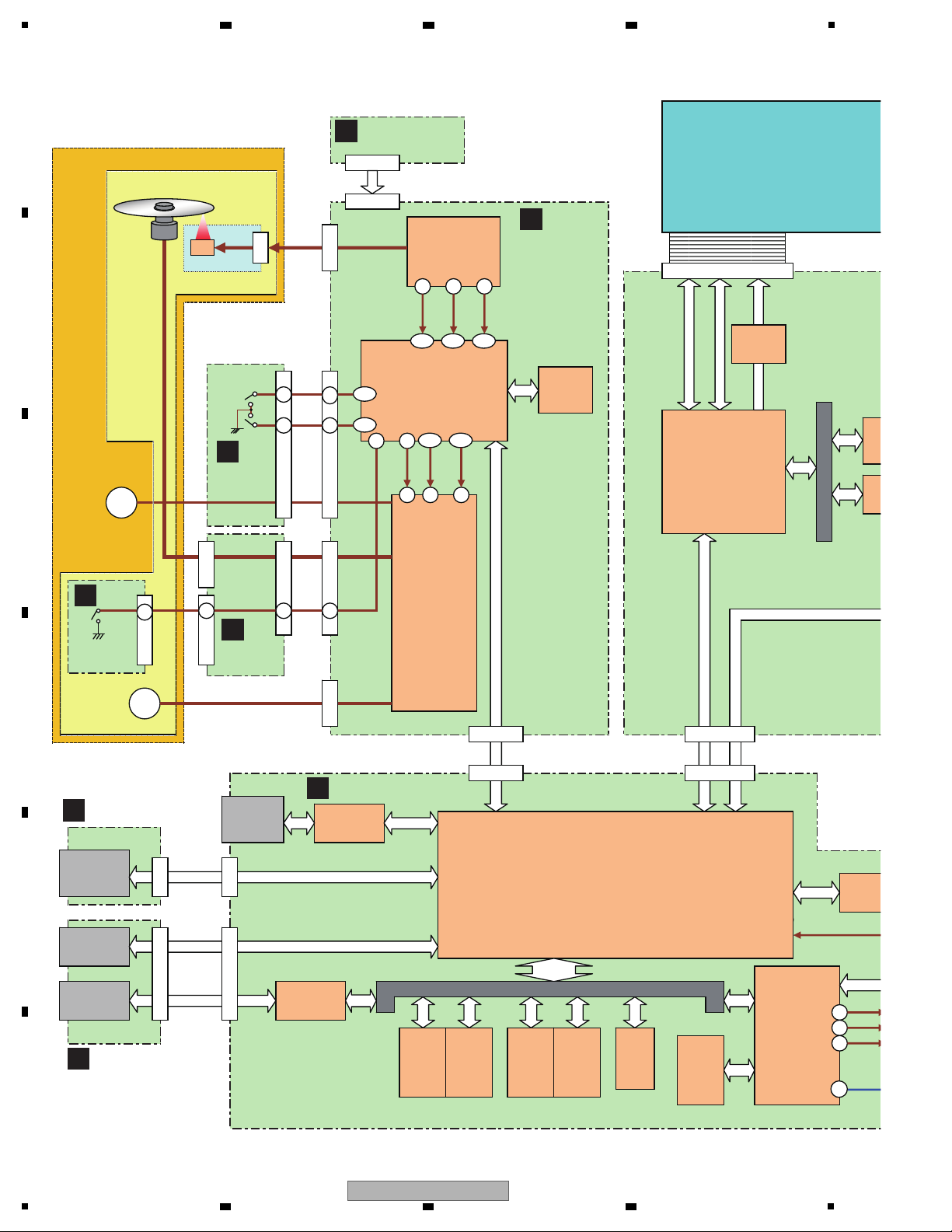
CPU : MAIN->TFT
CLK: 6MHz
CPU : MAIN->PANEL
CPU : TFT->MAIN
CLK: 1MHz
ATAPI
Serial (SSI0 only) (SSI1 : no use)
PICKUP ASSY
Control
S/PDIF
LRCLK
DATA
BCLK
JA702
LAN
Connector
IC301
DSP
CLK:16.9344MHz
Core CLK:389.4912MHz
IC10
MAIN CPU
CLK:26.965MHz
Core CLK:323.58MHz
TFT-LCD MODULE
Host I/F
16
16
MAIN System Bus
K3
T3
K4
D8
16
JA6301
USB-A Jack
CN5101
SD Card
Connector
CN704
IC7006
SODC
CLK:16.934MHz
IC7004
128kB
FLASH
8
112109111
IC7002
FEP
15 19 29
175
176
IC7001
6ch
Servo Driver
119 120
62
46 5 4
RFENV
FE
TE
TEDRV
FEDRV
LOAD
CN701
CN7005
OEIC
CN7001
MM
CN 9001
CN 7003
4
5
4
5
LOADING
MOTOR
MM
CN6101
CN6103
CN7009
CN6001
1
1
1
13
CN7004
STEPPING
MOTOR SK
TRAVERSE MECHANISM
SLOTIN MECHA ASSY
CN6102
CN2
CN7302
POWER
CN4002
LPS2
IC4001
TFT CPU
CLK:24.576MHz
Core CLK:393.216MHz
16
TFT S
y
stem Bus
16
16
CN4013
Se
6
INSW
IC1
Authent
IC
SPINDLE
MOTOR
JA6302
USB-B Jack
IC302
32MB
SDRAM
Bus CLK
129.8304MHz
IC3
4MB
FLASH
16
IC1
32MB
SDRAM
Bus CLK
107.86MHz
16 16
IC12
32MB
SDRAM
Bus CLK
107.86MHz
IC13
32MB
SDRAM
Bus CLK
107.86MHz
16
16
CS1
CS2 CS0
CS3
CN6301
CN703
CN5102
CN702
U-HPI
32M
Bus C
2M
I2C
IC701
USB-B IC
CLK:48MHz
IC704
Ether PHY
CLK:25MHz
MII , MDC
CD
LPS1
Universa
Host-Port
Interface
IC4018
Backlight
Power
IC2
32MB
SDRAM
Bus CLK
107.86MHz
T
POWER SUPPLY
ASSY
A
SRVB ASSY
E
MAIN ASSY
G
SDCB ASSY
H
USBB ASSY
D
SLMB
ASSY
C
INSW
ASSY
B
SPCN
ASSY
RGB 5bit
Sync.
SDHC I/F (CLK: 27 MHz)
USB Full/High Speed I/F
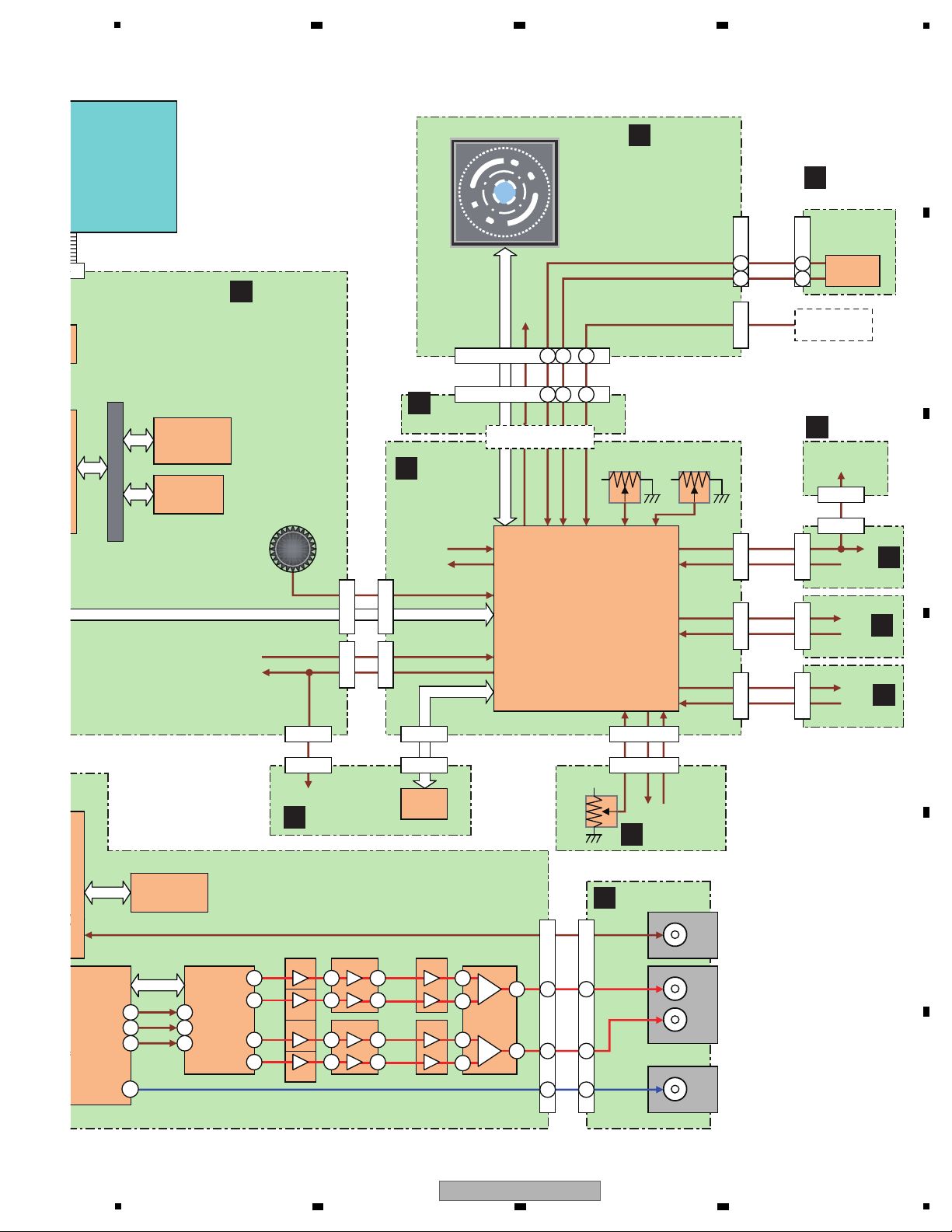
4.2 SIGNAL BLOCK DIAGRAM
A
B
C
2 3 4
D
E
F
12
1
2 3 4
CDJ-2000NXS
5
OPAMP
OPAMP
FET AMP
Q504
Control
JA9402
Analog out
JA9403
Digital out
JA9401
Control out
Lch
Rch
S/PDIF (Digital Audio) (fs=44.1kHz const.)
LRCLK
DATA
BCLK
CN501
IC505
DAC
CLK:16.9344MHz
IC301
DSP
MODULE
K3
T3
K4 1
2
3
D8
IC503
IC502
IC504
12
10
5
1
7
Analog Audio
CN9401
4
2
9
16
TFT S
y
stem Bus
16
16
LED
KEY
Serial (Syncronus)
LED KEY
LED
KEY
TCH
JOG2
JOG1
LED
KEY
IC5001
CDC IC
JH8003
JH8701
JH8002
CN8651
PC9301
Encorder
JH9202
CN9301
4
3 3
4
Serial (Syncronus)
VR8001
TOUCH / BRAKE
VR8002
RELEASE / START
VR8701
TEMPO SLIDER
CN4007
CN8002
S4028
Rotary Search
IC14
Authentication
IC
U-HPI
Vinyl
IC4005
32MB SDRAM
Bus CLK : 98.304MHz
IC4004
2MB FLASH
I2C
CN8001
CN4012
CN5002
CN4015
LED
LED
KEY
JH8001
CN8601
JH8004
CN8502
LED
CN8501
CN6201
CN8003
CN5001
Serial
LED
CN9203
SHEET SW
JUMPER
CN8801
JH9201
511
12
51112
LED
KEY
IC8003
PANEL CPU
(Within FLASH)
CLK:15.975MHz
Q503
Q505
Q506
FET AMP
Q518
Q517
5
2
3
6
1
6
1
7
7
2
2
6
R
L
Digital Audio
Control
16
17
12
13
JOG FL
Universal
Host-Port
Interface
t
J
PNLB ASSY
I
TFTB ASSY
K
JFLB ASSY
S
INDB ASSY
R
JOGB ASSY
Q
KSWB ASSY
P
CNCT ASSY
O
EUPB ASSY
L
CDCB ASSY
M
SDSW ASSY
N SLDB ASSY
F
JACB ASSY
6 7 8
A
B
C
D
5
CDJ-2000NXS
6 7 8
E
F
13
1
Spindle
Traverse Mecha ASSY
Power Cable AC Inlet ASSY
Motor
EARTH
LIVE/NEAUTRAL
PickUp
Others
IC7002
132
7
9 10
AC
IC7301
12V -> 5.14V
IC7302
12V -> 3.34V
6
4
5
6
4
5
V+12_EUP
CN7302
V+12
V+12S
P
1210
11
6
4 3
CN705
CN7301
V+12_EUP
V+3R3
1
7
3
13
7
11
CN501CN9401
IC705
12V -> 1.265V
13
15
17
18
1
14
16
CN702
CN704 CN4002
IC7010
12V -> 5V
IC9401
12V -> -12V
V+1R2
V+12_EUP
IC7005
5V -> 1.5V
IC7003
5V -> 3.3V
3.3V -> 1.65V
5V -> 2.2V
V+5A
V+3
A
V+3D
VREF1
VHALF
V+5
V+1R5D
P7003
P7302
P7001
P
P9401
P
P9402
P
V+12S
V+5_DAC
V+12
CN1
CN2
S9101
AC CN9101
Chassis
IC7305
12V -> 5.10V
P
V+3R3
V+12_EUP
V+5
V+12
V+3R3
V+12
CN7303
1
2
CN7001
V+3A
CN7009
1
13
CN6101
12
V+5
V+5
V+5_DAC
IC9403
12V -> 5V
V-12
V-12
V+5
V+3R3
V+3R3
V+12
V+12
10
1
CN6302
1
2
CN5101
SD Card
Connector
V+3R3
V+5_USB_D
V+5_USB_D
V+5_USB_D
V+5_USB_D
V+5_USB_D
V+5_USB
CN5102
CN6102
V+5A
V+5
V+3R3
V+12
V+1R2
IC6301
Current
Detect
JA6301
USB-A
Connector
V+5
V+1R2
17
15
13
12
29
16
14
3
4
For
/UXJCB
Power Cable AC Inlet ASSY
LIVE/NEAUTRAL
For
/SYXJ8, /AXJ5
/FLXJ , KXJ5
U
ACIN ASSY
A
SRVB ASSY
B
SPCN ASSY
T
POWER
SUPPLY
ASSY
E
MAIN ASSY
F
JACB ASSY
G
SDCB ASSY
I
TFT
H
USBB ASSY
2 3 4
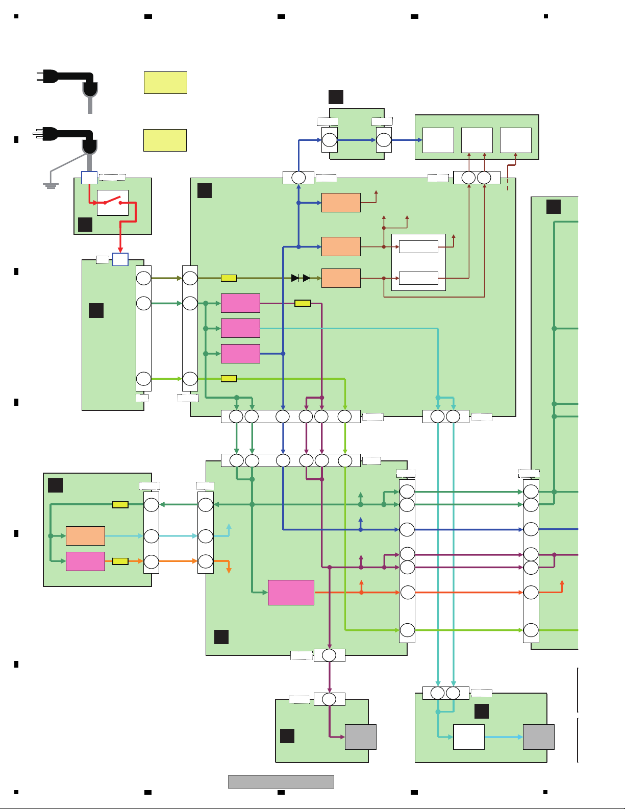
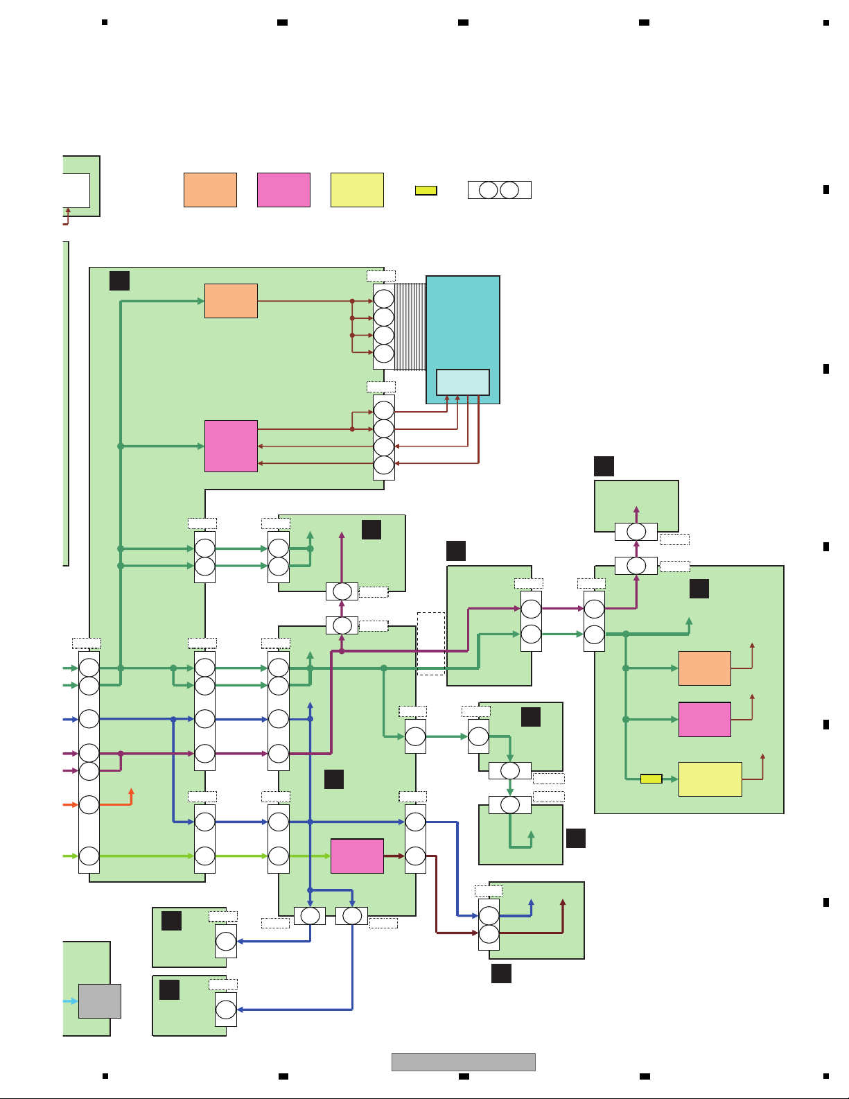
4.3 POWER SUPPLY BLOCK DIAGRAM
A
B
C
D
E
F
14
1
2 3 4
CDJ-2000NXS
CN4002
CN4007
CN8003
8
1
2
2
JH9202
CN9301
IC8002
12V -> 3.3V
IC9203
12V -> 27V
IC9204
12V -> 3.3V
IC9202
12V -> AC2.7V
V+5
7
8
6
5
V+3R3FL
V+27
VFDP2R7
V+3R4_LCD
7
6
IC4018
12V -> 15.6V
IC4019
12V -> 3.4V
CN4014
CN4013
3
2
JA6301
USB-A
Connector
V+1R2
ANODE1,2
CATHODE1
CATHODE2
V+5
V+12
CN4012
CN8001
CN8002
V+12_EUP
V+3R3
V+5
V+12
V+12
V+5
8
1
7
JH8003
17
15
13
12
29
16
14
17
19
21
20
3
1
17
19
21
20
1
3
CN4015
3
4
CN5002
2
1
V+5
CN5001
7
V+12
V+3R3
JH8701
V+3R3EV+5
V+3R3E
V+5
CN8502
V+12
V+12
V+3R3
V+12
V+3R3
P
P9201
V+12
4
CN8501
1
CN6201
JH8004
7
7
1
10
1
10
JH9201CN8801
1
CN8601
5
CN8651
JH8001
1
JH8002
5
DCDC
Converter
Regulator
Notes
DCAC
Converter
P
Protector
1 5
Connector&Pin No.
V+12
V+12
V+3R3
V+12
Jumper
Backlight
O
EUPB
ASSY
I
TFTB ASSY
J
PNLB ASSY
R
JOGB ASSY
P
CNCT ASSY
L
CDCB
ASSY
M
SDSW
ASSY
N
SLDB ASSY
Q
KSWB
ASSY
S
INDB ASSY
K
JFLB ASSY
TFT LCD
5
6 7 8
A
B
5
C
D
E
CDJ-2000NXS
6 7 8
F
15
1
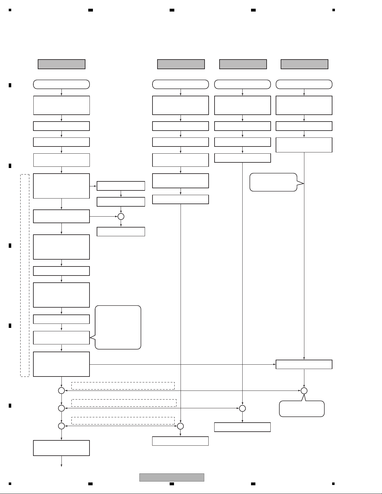
Power on Power on
Pin Y22 of Main CPU
(IC101) cancels reset
at H.
Program transfer from
FLASH to SDRAM
Canceling DSP reset
from pin B18 of Main
CPU. Pin G2 of DSP
(IC501) becomes "H".
Canceling ETH_PHY reset
from pin A18 of Main
CPU. Pin 42 of ETH_PHY
(IC1304) becomes "H".
Canceling USB_B reset
from pin A17 of Main
CPU. Pin 46 of USB_B
(IC1101) becomes "H".
Canceling ATAPI reset
from pin C10 of Main
CPU. Pin 173 of SODC
(IC7006) becomes "H".
Program transfer to
DSP
Register setting of ETH_PHY
Register setting of USB_B
Initialization of the
built-in peripherals
Initialization of the SDRAM
Initialization of the SDRAM
Initialization of the DSP
Initialization of the DAC
Initialization of the peripheral device
Initialization of the Main CPU
Pin 13 of TFT CPU
(IC4001) cancels reset
at H.
Program transfer from
FLASH to SDRAM
Pin 12 of PNL CPU
(IC8003) cancels reset
at H.
Pin 45 of SODC
(IC7006) cancels reset
at H.
Initialization of the SDRAM
Initialization of the TFT CPU
Display an opening screen
Initialization of the
peripheral device
Power on
Initialization of the JOG_FL
Initialization of the PNL CPU
Initialization of the CDC
Power on
Initialization of the
loading mechanism
Initialization of the ATAPI
LED initial lighting
Device select screen
Canceling reset
Apple
authentication
chip
Communication between Main CPU and SRVO
Initialization of the SODC
The insertion of the
disk is possible.
The insertion of the
disk is possible.
Built-in peripherals
• USB_A
• ETH_MAC
• SD
• ATAPI
• SERIAL
• SSI
Communication between Main CPU and PNL CPU
Communication between Main CPU and TFT CPU
MAIN CPU TFT CPU PANEL CPU SRVO
2 3 4
5. DIAGNOSIS
5.1 POWER ON SEQUENCE
A
B
C
D
E
F
16
1
2 3 4
CDJ-2000NXS
5
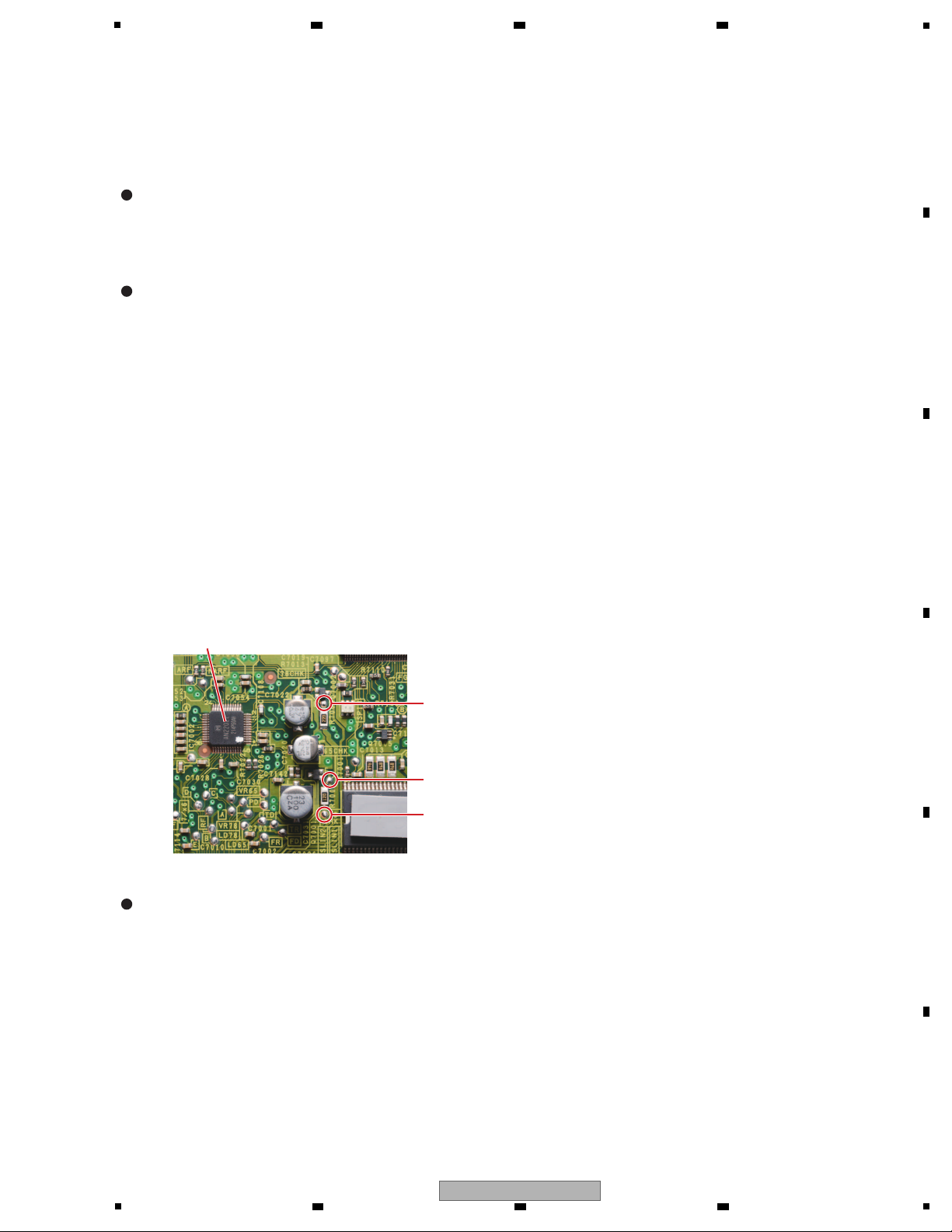
Measure the voltage at the probe pad on the SRVB Assy (see the photo below), using a tester.
∗ To check lighting of each LD, follow the procedure indicated in "[7] Checking the servo operations of the drive unit" in
"6.1 SERVICE MODE."
∗ Note that the LD may be degraded if the probes of a tester are applied to or pulled away from the probe pad with the LD ON.
Check method
Directly measure the resistance value of the actuator, using a tester.
* Before measuring, short-circuit the LD short-circuit pads.
Note that the LD may be degraded if connection/disconnection of CN7001 is performed with the LD short-circuit pads open.
• Focus side
Disconnect* the FFC connected to the CN7001 then measure the resistance value between FFC pins 23 and 24.
• Tracking side
Disconnect* the FFC connected to the CN7001 then measure the resistance value between FFC pins 21 and 22.
Check method
1. With the LD OFF, apply the probes of a tester to the reference probe pad (LDCHK) and 78CHK (CD side) or 65CHK
(DVD side).
2. With the probes kept applied to the above-mentioned pads, turn the LD ON to measure the voltage between them.
3. After measurement, turn the LD OFF (ALL OFF) then pull the probes away.
4. Calculate the current value by dividing the measured voltage value by the resistance value mentioned below.
(For CDs: R7008 = 22 ohms, For DVDs: R7007 = 12 ohms)
Procedures
If the calculated current value exceeds the maximum value, the LD has been degraded
Failure judgment:
A value out of the range of the specifications is judged as failure.
Failure judgment:
78CHK
65CHK
IC7002
Fig.1 SRVB Assy
LDCHK
LD power after passing through the objective lens [mW]
SPEC: DVD 0.180 ± 0.03
CD 0.210 ± 0.03
Check method: Measure the LD power, using an optical power meter.
Failure judgment: A value out of the range of the specifications is judged as failure.
Actuator resistance value [ohms]
Specifications on the focus side: 3.7 ±0.55
Specifications on the tracking side: 4.3 ±0.65
LD current [mA]
SPEC: DVD TYP50 MAX70
CD TYP65 MAX75
This unit has self-diagnostic functions for the drives.
For drive-related malfunctions, first perform the self-diagnostics to check the drives in Service mode. If the results indicate any
problem with the drives, check the following items:
6 7 8
5.2 FAILURE JUDGEMENT OF THE PICKUP ASSY
A
B
C
D
E
5
6 7 8
CDJ-2000NXS
F
17
1
1 ————— ————— Check for the location of a defect in
Service mode.
See the section describing locations of defects in
this manual.
6.1 SERVICE MODE
In this section, causes of failure, diagnostics points, and corrective measures can be searched for according to symptoms.
Before disassembling this unit, it is recommended to infer a failure point by performing a status check and referring to the error
code.
For the relationship of each power-supply and signal system, see “4. BLOCK DIAGRAM,” and “10. SCHEMATIC DIAGRAM.”
If software of the product is updated before performing diagnostics, check that software updating has been performed properly
before proceeding to diagnostics.
If software updating has not been performed properly, update the software, following the instructions in [9] Firmware update of
“6.1 SERVICE MODE.”
Contents
[0] Prior Confirmation
[1] Failure in Startup
[2] Display (JOG FL/LED)
[3] Operations (SW/Volume/JOG/CDC/Rotary Encoder)
[4] USB (Type A/Type B), SD Card
[5] LAN
[6] ATAPI DRIVE
[7] AUDIO OUT
[8] CONTROL
[9] DRIVE Assy
[10] EUP Mode
[11] SERVICE MODE
[12] Error Codes
[0] Prior Confirmation
[0-1] Checking in Service Mode
1 Disconnection,
breakage, or
loose connection
of cables
Cables Check that all the cables are securely
connected.
Check that there is no breakage in the
cables.
Securely connect the cables. If a cable is broken,
replace it.
4.1 OVERALL
WIRING DIAGRAM
10. SCHEMATIC
DIAGRAM
[0-3] Checking Cables
1 ————— Alarm port on
the MAIN Assy
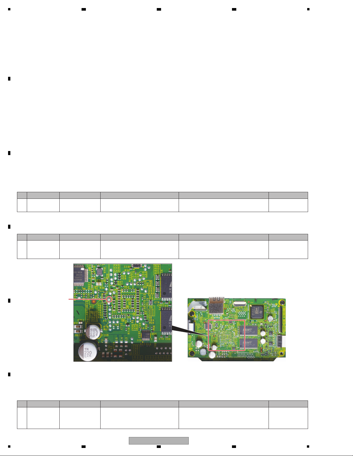
(Fig. 1)
Check the output waveforms from the
alarm port.
If an output waveform is judged to be improper,
see the section describing locations of defects in
this manual.
6.1 SERVICE MODE
_[8] Outputs of the
Alarm Port
[0-2] Checking the Alarm Port
If “[0-1] Checking in Service Mode” is performed, this check is not required.
Fig. 1
MAIN Assy
Alarm port
No. Cause Diagnostics Point Item to be Checked Corrective Action Reference
No. Cause Diagnostics Point Item to be Checked Corrective Action Reference
No. Cause Diagnostics Point Item to be Checked Corrective Action Reference
2 3 4
5.3 TROUBLESHOOTING
A
B
C
D
E
F
18
1
2 3 4
CDJ-2000NXS
5
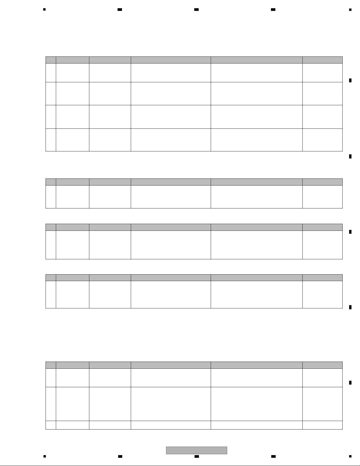
[1] Failure in Startup
[1-1] No power
[2] Display (JOG FL/LED)
[2-1] The JOG FL does not light.
The JOG FL and the LEDs are controlled by the PANEL CPU (IC8005).
[1-2] Indications on the LCD
Check the indications on the LCD.
Nothing is displayed on the LCD. (Black screen)
Indications on the LCD are in white screen.
1 The SW power
does not function
properly.
SRVB Assy Check V+12_EUP. If V+12_EUP (CN7301 pin_1) is not output, the
SW power is defective. Replace it.
—————
2 The SW power
does not function
properly.
PNLB Assy Check V+3R3_PNL.
The regulator IC (IC8002) may be loosely connected
with its peripheral devices or a part may be defective.
Correct loose connection. If the symptom persists,
replace the defective part.
—————
4 Various power
supply ICs do
not function
properly.
SRVB Assy,
MAIN Assy
Check each power-supply IC.
The regulator IC and its peripheral devices for each
power supply may be loosely connected or a part
may be defective. Correct loose connection.
If the symptom persists, replace the defective part.
—————
3 The EUP control
unit does not
function properly.
SRVB Assy Check the EUP_CONT signal. If the signal is L, check the output of the SW
power. If V+12 (CN7301 pin_2) is not output,
the SW power is defective. Replace it.
If the signal is H, see [10] EUP Mode.
—————
1
Power supply for
the backlight is
not input properly.
TFTB Assy
Check the connection on the V+12T line and
check the mounting status of the peripheral
parts of the backlight power circuit.
The V+12T line may be loosely connected or the
backlight power circuit may be defective.
Correct loose connection.
If the symptom persists, replace the defective part.
10.11, 10.12
TFTB ASSY
1
Power is not
supplied properly.
JFLB Assy Check the power-supply voltages (V+3R3,
VFDP2R7_F1, VFDP2R7_F2, and V+27)
of the FL.
Each power-supply may be loosely connected or
may be defective. Correct loose connection. If the
symptom persists, replace the defective part.
—————
3
Defective JOG FL
————— If the symptom persists after the above
corrections,
Replace the JOG FL. —————
2 Defective
control signal
JFLB Assy Check that the FL control line is properly
connected in the JFLB ASSY.
• J_SCLK
• J_BK
• J_LAT
• J_DSO
Check the connection and correct loose
connection.
As the JOG FL is controlled by the PANEL CPU,
if no signal is output, check the PANEL CPU.
—————
Startup stops with the “Pioneer” logo displayed.
1
Communication
between the MAIN
CPU and TFT CPU
could not be
established.
TFTB Assy,
MAIN Assy
Check the serial communication cable
connection between the MAIN CPU and
TFT CPU.
Diagnose the TFT CPU and its peripherals,
referring to [12-5] E-7023: GUI CPU ERROR.
—————
1
The TFT CPU
does not function
properly.
TFTB Assy Check the power supply and signals
around the TFT CPU.
• V+3R3T_BF, V+1R2_BF
• RESET_TFT
• BUSCLK (Approx. 98 MHz)
Diagnose the TFT CPU and its peripherals,
referring to [12-5] E-7023: GUI CPU ERROR.
—————
No. Cause Diagnostics Point Item to be Checked Corrective Action Reference
No. Cause Diagnostics Point Item to be Checked Corrective Action Reference
No. Cause Diagnostics Point Item to be Checked Corrective Action Reference
No. Cause Diagnostics Point Item to be Checked Corrective Action Reference
No. Cause Diagnostics Point Item to be Checked Corrective Action Reference
6 7 8
A
B
C
D
E
5
6 7 8
CDJ-2000NXS
F
19
1
[2-2] An LED does not light.
1 Defective SW PNLB Assy Check if there is loose connection on the
signal line from the PANEL CPU (IC8003)
up to the SW.
If there is no loose connection and if the signal
does not become L when the SW is pressed,
that SW is defective. Replace it.
—————
2 Defective PANEL
CPU
PNLB Assy If the symptom persists after the above
corrections.
Check the connection of the PANEL CPU
(IC8003). If the connection is OK, the port may
be damaged. Replace it.
—————
2 Defective PANEL
CPU
PNLB Assy If the symptom persists after the above
corrections.
Check the connection of the PANEL CPU
(IC8003). If the connection is OK, the port may
be damaged. Replace it.
—————
2 Defective PANEL
CPU
PNLB Assy If the symptom persists after the above
corrections.
Check the connection of the PANEL CPU
(IC8003). If the connection is OK, the port may
be damaged. Replace it.
—————
1 Defective SW PNLB Assy Check if there is loose connection on the
signal line from the PANEL CPU (IC8003)
up to the SW.
If other SWs connected to the same port on the
PA NEL CPU (IC8003) function properly and if
connection is properly made, replace the SW.
—————
2 Defective
MAIN CPU
MAIN Assy If the symptom persists after the above
corrections.
The MAIN CPU (IC10) is defective.
Replace the MAIN Assy.
—————
1 Defective SW SDSW Assy,
MAIN Assy
Check if there is loose connection on the
signal line from the MAIN CPU (IC10)
up to the SW.
If there is no loose connection and if the signal
does not become L when the SW is pressed,
that SW is defective. Replace it.
—————
1 Defective
Tempo slider
SLDB Assy,
PNLB Assy
Check the waveform of signals on the
signal line (ADCT, ADIN).
If the voltage on the signal line (ADIN) fluctuates
within the range of 0–3.3 V, with 1.65 V at the
center, go to Step 2. If it does not, the Tempo
slider (VR8701) is defective. Replace it.
—————
2 Defective PANEL
CPU
PNLB Assy If the symptom persists after the above
corrections.
Check the connection of the PANEL CPU
(IC8003). If the connection is OK, the port may
be damaged. Replace it.
—————
1 Defective VOL PNLB Assy Check the connections of and waveforms
of signals on the signal lines (TCH/BRK)
and (RELS/ST).
If the voltage on the signal line (TCH/BRK and
RELS/ST) fluctuates within the range of 0–3.3 V,
go to Step 3. If it does not, the TOUCH/BRAKE
(VR8001) and RELEASE/START (VR8002) are
loosely connected or defective. Connect them
properly or replace them.
—————
1 Defective LEDs LED in question
Check that soldering at the LED in question
is properly made. If it is OK, check that the
forward voltage (2.2 - 2.7 V) is present at
both ends of the LED.
Correct any defective soldering.
If the forward voltage is present, then the LED
itself is defective. Replace it.
—————
2 Defective drive
circuit
Transistor in
question
Check that the control signal for the LED in
question is output from the PANEL CPU (IC8003).
If the LED does not light even if the control signal is
output properly, then the transistor is defective. Replace it.
—————
3 Defective PANEL
CPU
PNLB Assy If the symptom persists after the above
corrections.
Check the connection between the PANEL CPU
(IC8003) and the LED in question. If the connection
is OK, the port may be damaged. Replace it.
—————
[3] Operations (Keys/variable controls/JOG)
[3-1] No key functions.
[3-2] Variable controls not controllable
As operations of all keys, variable controls, and JOG dial can be checked in Service mode, it is recommended to check operations of
those controls in Service mode before proceeding to the subsequent checks. (For details, refer to 6. SERVICE MODE.)
The PLAY, CUE, AUTO BEAT LOOP, BEAT SELECT, REV, LOOP IN, LOOP OUT, or RELOOP key does not function (direct input).
Other keys (except for the USB STOP key) do not function. (Because of A/D input, multiple SWs are connected to the same port on the PANEL CPU.
The USB STOP key does not function. (The signal from the USB STOP key is input to the MAIN CPU.)
Tempo slider not controllable
TOUCH/BRAKE and RELEASE/START not controllable
No. Cause Diagnostics Point Item to be Checked Corrective Action Reference
No. Cause Diagnostics Point Item to be Checked Corrective Action Reference
No. Cause Diagnostics Point Item to be Checked Corrective Action Reference
No. Cause Diagnostics Point Item to be Checked Corrective Action Reference
No. Cause Diagnostics Point Item to be Checked Corrective Action Reference
No. Cause Diagnostics Point Item to be Checked Corrective Action Reference
A
2 3 4
B
C
D
E
F
20
1
2 3 4
CDJ-2000NXS
5
[3-3] The NEEDLE SEARCH does not work.
1
Loose connections
in the communication
line
CDCB Assy Check the connections of the peripheral
circuits of the CDC (IC5001).
The communication line may be loosely
connected. Correct it if it is.
—————
2 Defective CDC PNLB Assy
Check that the signal from Pin 5 of CN8003
changes when the NEEDLE SEARCH pad
is touched. (When the pad detects touching
by a finger, this signal is first output from
CDC to the PANEL CPU.)
The CDC (IC5001) may be defective.
Replace it.
—————
3 Defective PANEL
CPU
PNLB Assy If the symptom persists after the above
corrections.
Check the connection of the PANEL CPU
(IC8003). If the connection is OK, the port may
be damaged. Replace it.
—————
2 Defective PANEL
CPU
PNLB Assy If the symptom persists after the above
corrections.
Check the connection of the PANEL CPU
(IC8003). If the connection is OK, the port may
be damaged. Replace it.
—————
No response when the NEEDLE SEARCH is touched
[3-4] The rotary encoder does not work.
1
Loose connections
in the signal line
or defective SW
TFTB Assy,
PNLB Assy
Check the connections of the signal lines for
ENC_SW, ENC1, and ENC2. When the SW is
pressed, the ENC_SW signal must become L,
and when it is turned, the waveforms of the
signal lines for ENC1 and ENC2 must change.
The PANEL CPU (IC8003) and SW may be
loosely connected or they may be defective.
Reconnect them securely.
If the symptom persists, replace them.
—————
1 Defective photo
interrupter or
PA NEL CPU
JOGB Assy,
JFLB Assy,
CNCT Assy,
PNLB Assy
Check the waveforms of the signal lines
(JOG1/JOG2).
If no waveform can be confirmed, the photo interrupter
(PC9301) may be defective. Replace it.
If a waveform can be confirmed, the signal line may be
loosely connected or the PANEL CPU (IC8003) may
be defective. Reconnect the signal line.
If the symptom persists, replace it.
10.20 WAVEFORMS
a b
2 Defective
encoder plate
JOG Assy Check if the encoder plate has come off
Gear A or is dirty.
If it has come off, adhere it at its original position.
If it is dirty, replace it with a new one.
—————
2 Defective
SW ring
and
JOG holder
JOG Assy Check if there is any foreign object
between the SW ring and JOG holder.
Remove any foreign object, if present. —————
Check if the cushions that are adhered to
the JOG holder and SW ring have worn
out.
Replace the SW cushion with a new one. —————
No response when the rotary encoder is operated
[3-5] Abnormalities regarding the JOG dial
Turning of the JOG dial is not detected
1 Defective photo
interrupter or
PA NEL CPU
JOGB Assy,
JFLB Assy,
CNCT Assy,
PNLB Assy
Check the waveform of the signal on the
signal line (JOG_SW) when the JOG dial
is pressed.
If the signal on the signal line (JOG_SW) is not set to
L when the JOG dial is pressed, the Sheet SW
may be defective. Replace it.
If the signal line is set to L, the signal line may be
loosely connected or the PANEL CPU (IC8003) may
be defective. Reconnect the signal line.
If the symptom persists, replace it.
—————
Pressing on the JOG dial cannot be detected.
1 Defective
JFLB Assy
or
gears
JOG Assy Check if the JOG FL of the JFLB has
been shifted upward from the holder.
The JOG FL may interfere with JOG A.
Replace the JFLB Assy.
—————
There may be any scratches on the 3
gears or some foreign object between
the gears.
If there are any scratches, replace the scratched
gear with a new one. If there is any foreign object,
remove it then replace the gears with new ones.
After that, check that the JOG adjustment value is
within the reference range, referring to “8.3 JOG
DIAL ROTATION LOAD ADJUSTMENT.”
—————
Noise is heard when the JOG dial is turned.
No. Cause Diagnostics Point Item to be Checked Corrective Action Reference
No. Cause Diagnostics Point Item to be Checked Corrective Action Reference
No. Cause Diagnostics Point Item to be Checked Corrective Action Reference
No. Cause Diagnostics Point Item to be Checked Corrective Action Reference
No. Cause Diagnostics Point Item to be Checked Corrective Action Reference
6 7 8
A
B
C
CDJ-2000NXS
5
6 7 8
D
E
F
21
1
1 Improper adjust-
ment
or assembly
of the JOG dial
JOG Assy Check that the load value for the JOG dial
is within the specified range, referring to
“Measuring method” in “8.3 JOG DIAL
ROTATION LOAD ADJUSTMENT.”
If it is outside the specified range, adjust the position
of the Adjust Plate to change the load value for the
JOG dial, referring to “How to Adjust” in “8.3 JOG DIAL
ROTATION LOAD ADJUSTMENT.”
—————
During the above adjustment, if the upper-limit
adjustment position of the Adjust Plate is reached,
oil mayhave been spattered on the Adjust Plate.
Replace the washer, gear, and cam plate with new
ones, then reassemble. After replacement, adjust
the position of the Adjust Plate to change the load
value for the JOG dial.
—————
The JOG dial turns too freely. (The load value for the JOG dial is outside the specified range.)
1 Improper adjust-
ment of the JOG
dial or defective
washer, gear, or
cam plate
JOG Assy Check that the load value for the JOG dial
is within the specified range, referring to
“Measuring method” in “8.3 JOG DIAL
ROTATION LOAD ADJUSTMENT.”
If it is outside the specified range, adjust the position
of the Adjust Plate to change the load value for the
JOG dial, referring to “How to Adjust” in “8.3 JOG DIAL
ROTATION LOAD ADJUSTMENT.”
—————
During the above adjustment, if the lower-limit
adjustment position of the Adjust Plate is reached,
shavings from the worn-out washer may have
increased the friction. Replace the washer, gear,
and cam plate with new ones, then reassemble.
After replacement, adjust the position of the Adjust
Plate to change the load value for the JOG dial.
—————
Resistance to turning the JOG dial is too strong. (The load value for the JOG dial is outside the specified range.)
1 Improper adjust-
ment
or assembly
of the JOG dial
JOG Assy Check if the plate spring of the JOG
holder is worn out or deformed.
Replace the JOG holder. After replacement,
adjust the position of the Adjust Plate to
change the load value for the JOG dial.
—————
Check if there is any foreign object in
the link section (gears).
Remove the foreign object. During reassembly,
pay attention to the position of the cam plate.
After replacement, adjust the position of the Adjust
Plate to change the load value for the JOG dial.
—————
1
Loose connections
in the communication line.
Between USBA Assy
and MAIN Assy
Check the connection of the USB
communication line.
If connection is improper, resolder it.
If connection is proper, go to 2.
—————
4 Defective
MAIN CPU
MAIN Assy If the symptom persists after the above
corrections.
The MAIN CPU (IC10) is defective.
Replace the MAIN Assy.
—————
2 Defective
MAIN CPU
MAIN Assy Check the signal from the MAIN CPU and
USB CONTROLLER.
If the signal is not output from the MAIN CPU
(IC10), it may be defective.
Replace the MAIN Assy.
—————
3
The USB
POWER SW IC
or its control
signal is defective.
USBB Assy Check the CPU_USB_HSTPWREN and
CPU_USB_HSTPWRFL signals from the
USB POWER SW IC (IC6301).
If the CPU_USB_HSTPWREN signal does not become H,
check the connection. If the connection is OK, then the
MAIN CPU (IC10) is defective. Replace the MAIN Assy.
If the CPU_USB_HSTPWRFL signal does not become H,
the USB POWER SW IC (IC6301) is in a state of
shutdown caused by abnormally high temperature.
Check the connection. If the connection is OK, then the
port may be damaged. Replace it.
—————
2
V+5_USB_HOST_
VBUS is defective.
MAIN Assy Check V+5_USB_HOST_VBUS of the
USB power supply.
If V+5_USB_HOST_VBUS cannot be confirmed, go to 3.
If V+5_USB_HOST_VBUS can be confirmed, go to 4.
—————
The ADJ KNOB does not work or does not stop at the intended position.
[4] USB (Type A/Type B), SD Card
[4-1] No communication via the USB connector (Type A)
Check the following, with a USB device connected to the USB A connector.
1
Loose connections
in the communication line.
MAIN Assy Check the connections from the MAIN
CPU and USB CONTROLLER.
If connection is improper, resolder it.
If connection is proper, go to 2.
—————
3
Loose connections
in the USB signal.
MAIN Assy Check the connections of the
communication line (USB_D+, USB_D-).
The communication line may be loosely
connected. Correct it if it is.
—————
4
Defective
USB CONTROLLER
MAIN Assy If the symptom persists after the above
corrections.
The USB CONTROLLER (IC701) is defective.
Replace it.
—————
[4-2] No communication via the USB connector (Type B)
Check the following, with a USB device connected to the USB B connector.
No. Cause Diagnostics Point Item to be Checked Corrective Action Reference
No. Cause Diagnostics Point Item to be Checked Corrective Action Reference
No. Cause Diagnostics Point Item to be Checked Corrective Action Reference
No. Cause Diagnostics Point Item to be Checked Corrective Action Reference
No. Cause Diagnostics Point Item to be Checked Corrective Action Reference
A
2 3 4
B
C
D
E
F
22
1
CDJ-2000NXS
2 3 4
5
1
Loose connections
in the communication line.
SDCB Assy,
MAIN Assy
Check the connection of the SD serial
communication line.
If connection is improper, resolder it. —————
2 Defective
MAIN CPU
MAIN Assy If the symptom persists after the above
corrections.
The MAIN CPU (IC10) is defective.
Replace the MIAN Assy.
—————
3 Defective
MAIN CPU
MAIN Assy Check the periphery circuit of the MAIN
CPU.
Check the periphery of the MAIN CPU (IC10).
If no problem is found, the MAIN CPU may be
defective. Replace the MAIN Assy.
—————
1
Loose connections
in the communication line.
MAIN Assy Check the connection of the periphery
circuit of ETHER (IC704).
If connection is improper, resolder it. —————
2
Loose connections
in the communication line.
SRVB Assy,
MAIN Assy
Check the connection of the ATAPI lines. Check the connection between the MAIN CPU
(IC10) and SODC (IC7006). If no problem is
found, see “[9] DRIVE ASSY.” If the symptom
persists after those corrections, go to Step 3.
—————
2
Defective
ETHER PHY device
LAN jack
or
MAIN CPU
MAIN Assy If the symptom persists after the above
corrections.
The ETHER PHY device (IC704) or LAN jack
(JA702) may be defective.
Replace it. If the symptom persists, the MAIN
CPU (IC10) may be defective.
Replace the MAIN Assy.
—————
1 Improper
RESET signal
SRVB Assy,
MAIN Assy
Check the ATA_RESET signal (CN7005).
Communication will not start while the ATA_RESET signal
is L. Check the connection between the MAIN CPU (IC10)
and SODC (IC7006). If the connection is not properly made,
correct it. If no problem is found, see “[9] DRIVE ASSY.”
If the signal does not become H after those corrections, go
to Step 2.
—————
1
Power is not
supplied properly.
MAIN Assy,
JACB Assy
Check the power voltages (V+12A, V-12A,
V+5_DAC) for audio.
Each power-supply may be loosely connected or
may be defective. Correct loose connection.
If the symptom persists, replace the defective part.
—————
2 Defective
MUTE signal
MAIN Assy Check the signal from Pin 9 of CN501
(MUTE). Playback is muted when the si
gnal is at +12 V.
The connection, transistor, or DSP may be
defective. Correct loose connection. If the
symptom persists, replace the defective part.
—————
3
Loose connections
in the signal line.
MAIN Assy,
JACB Assy
Check the connection of the audio signal
lines (ROUT, LOUT).
If connection is improper, resolder it.
If connection is proper, go to 4.
—————
4
Power is not
supplied properly,
or the DAC or
DSP is defective.
MAIN Assy,
JACB Assy
Check the voltages (V+5, V+5_DAC) of
the DAC (IC505).
Each power-supply may be loosely connected or
may be defective. Correct loose connection.
If the symptom persists, replace the defective part.
—————
1
Loose connections
in the signal line.
MAIN Assy,
JACB Assy
Check the digital audio signal (SPDIF)
and its connection.
If connection is improper, resolder it. If the SPDIF
signal cannot be recognized, go to Step 3.
—————
3 Defective
MAIN DSP
MAIN Assy If the symptom persists after the above
corrections.
Replace the MAIN Assy. —————
2 Defective
transistor
MAIN Assy Check the digital audio signal
(SPDIF_OUT) and its connection.
If the SPDIF_OUT signal can be recognized, then the
transistor (Q504) may be defective. Check the connection.
If no problem is found, replace the transistor. If the
SPDIF_OUT signal cannot be recognized, check the
connection. If soldering is improper, resolder it.
—————
[4-3] The SD card cannot be recognized.
Check the following, with an SD card inserted in the SD connector.
[5] LAN
[5-1] No LAN communication
[6] ATAPI DRIVE
[6-1] No disc playback (Although loading and disc rotation can be performed properly, no track data are output.)
[7] AUDIO OUT
[7-1] No sound
Check the following, with a peripheral device connected to the Ethernet connector.
The analog audio signal is not output.
The digital audio signal is not output.
No. Cause Diagnostics Point Item to be Checked Corrective Action Reference
No. Cause Diagnostics Point Item to be Checked Corrective Action Reference
No. Cause Diagnostics Point Item to be Checked Corrective Action Reference
No. Cause Diagnostics Point Item to be Checked Corrective Action Reference
No. Cause Diagnostics Point Item to be Checked Corrective Action Reference
6 7 8
A
B
C
D
5
CDJ-2000NXS
6 7 8
E
F
23
1
1
Loose connections
in the signal line.
JACB Assy
Check the waveforms of the control signals
(CONT1, CONT2) from the CN9401 on the
JACB Assy.
If the signal cannot be recognized, the JACB Assy
may be defective. Check the soldering at the JACB
Assy then resolder it, if necessary.
If the signal can be recognized, go to Step 2.
—————
2 Defective
MAIN CPU
MAIN Assy
Check the waveforms of the control signals
(CONT01, CONT02) from the MAIN Assy.
If the input signal can be recognized, then the MAIN CPU
(IC10) may be defective. Replace the MAIN Assy. If the
input signal cannot be recognized, the communication
line or the peripheral devices may be loosely connected.
Resolder the terminals.
—————
1 Missing or
defective part
Loading mecha Check that there is no part missing or
defective.
If there is, install the missing part or replace the
defective part.
—————
2
Loose connections
in the signal line.
Loading mecha Check that the LP switch has been
mounted.
If soldering is improper, resolder it. —————
3 Improper
assembling
Loading mecha Check that the lever is engaged with the
LP switch.
Engage the lever with the LP switch. —————
4 Improper
soldering
Loading mecha Check that the wires from the loading
motor have been properly soldered.
If they are not soldered, solder them. —————
5 Power supply
error
SRVB Assy Check the power voltages (12 V, 5 V,
3.3 V, and 1.5 V).
Check the connection of the parts at the periphery of
the power-supply IC that does not output the voltage.
If the symptom persists after a corrective action, the
power supply block is defective. Replace it.
—————
7 MUTE1 and
MUTE2 signal
errors
SRVB Assy Check the waveforms of the MUTE1 and
MUTE2 signals. (During loading, the
MUTE1 signal is L and the MUTE2 signal
is H.)
DRIVER IC (IC7001) and SODC (IC7006) may
be improperly soldered or defective.
Resolder them, if necessary. If the symptom
persists, replace SODC (IC7006).
—————
9 Defective SRVB
Assy
————— If the symptom persists after the above
corrections.
Replace the SRVB Assy. —————
6 LPS1 and LPS2
signal errors
SRVB Assy
Check the waveforms of the LPS1 and LPS2
signal lines. (The LPS1 and LPS2 signals
becomes L when the SW is set to ON.)
The loading detection SWs (S8901 and S8902) may
be improperly soldered or defective. Resolder them,
if necessary. If the symptom persists, replace them.
5.4 OPERATIONAL
WAVEFORMS
2
8 LOAD signal
error
SRVB Assy Check the LOAD signal. DRIVER IC (IC7001) and SODC (IC7006) may
be improperly soldered or defective.
Resolder them, if necessary. If the symptom
persists, replace SODC (IC7006).
5.4 OPERATIONAL
WAVEFORMS
2
1
The main unit is
positioned inclined.
Main unit
Check if the main unit is positioned inclined.
Place it on a level surface. —————
3
Improper assembling
Traverse mecha Check the inside switch. Assemble the INSW Assy properly. —————
2
Improper assembling
Traverse mecha
Check if there is a missing or defective part at the
section where the main axis and stepper contact.
If there is, install the missing part or replace the
defective part.
—————
4 Power supply
error
SRVB Assy Check the power voltages (12 V, 5 V,
3.3 V, 1.5 V, VREF1, VREF2 and VHALF).
Check the connection of the parts at the periphery of
the power-supply IC that does not output the voltage.
If the symptom persists after a corrective action, the
power supply block is defective. Replace it.
—————
5INSW signal
error
SRVB Assy Check the INSW signal. (The INSW
becomes L when the INSW is set to ON.)
The FFC cables that connect the traverse mechanism,
SPCN, and SRVB are loosely connected, or the INSW
is defective. Reconnect them securely.
If the symptom persists, replace the INSW.
—————
6 MU1 signal error SRVB Assy Check that the MU1 signal becomes H
after loading is completed.
DRIVER IC (IC7001) and SODC (IC7006) may
be improperly soldered or defective.
Resolder them, if necessary. If the symptom
persists, replace SODC (IC7006).
—————
7
Improper assembling
Cables
Check that the FPC cable that connects the
traverse mecha and the SRVB Assy is
securely connected.
If it does not, securely connect it. If it is broken,
replace the traverse mecha.
—————
[8] CONTROL
[8-1] Improper fader operation after fader start
[9] DRIVE ASSY
[9-1] Improper operation of the loading mechanism
[9-2] The stepper does not work.
No loading
When it is thought abnormally, the drive section execute drive self-diagnose beforehand.
No. Cause Diagnostics Point Item to be Checked Corrective Action Reference
No. Cause Diagnostics Point Item to be Checked Corrective Action Reference
No. Cause Diagnostics Point Item to be Checked Corrective Action Reference
A
2 3 4
B
C
D
E
F
24
1
2 3 4
CDJ-2000NXS
5
1 Short-circuit pad Traverse mecha Check if the LD short-circuit pad is
short-circuited.
If it is, open it. —————
4INSW signal
error
SRVB Assy Check the INSW signal. (L at ON.) If the signal waveform is not proper, replace the
INSW Assy.
—————
5 MU1 signal error SRVB Assy Check that the MU1 signal becomes H
after loading is completed.
DRIVER IC (IC7001) and SODC (IC7006) may
be improperly soldered or defective.
Resolder them, if necessary. If the symptom
persists, replace SODC (IC7006).
—————
6 Improper
assembling
Traverse mecha Check if the objective lens is dirty. Clean the lens. —————
9 ————— ————— If the symptom persists after the above
corrections.
Replace the parts in the order of
(1) DRIVER IC (IC7001), (2) FEP (IC7002),
(3) SODC (IC7006), (4) SRVB Assy, then
(5) traverse mecha.
—————
2 7/x6 signal error ————— Check that the 7/x6 signal is H during
CD playback.
Check the connections between IC7006 and
CN7001. If soldering is improper, resolder it.
—————
3 E,F signal error SRVB Assy Check the E, F signals (CN7001).
Check that the signals fluctuate with 2.2 V at the center.
If a DC signal is not output, check the VREF1. If a DC
signal is not output from it, replace the FEP (IC7002).
If an AC signal is not output, check the soldering at the
CN7001–IC7002 of the pickup. If soldering is improper,
resolder it. If soldering is OK, replace the parts in the
order of (1) FEP (IC7002), (2) DRIVER IC (IC7001),
(3) SODC (IC7006), (4) SRVB Assy, then (5) traverse
mecha.
—————
7 A–F signal error SRVB Assy Check the A–F signals (CN7001).
Check that the signals fluctuate with 2.2 V at the center.
If a DC signal is not output, check the VREF1. If a DC
signal is not output from it, replace the FEP (IC7002).
If an AC signal is not output, check the soldering at the
CN7001–IC7002 of the pickup. If soldering is improper,
resolder it. If soldering is OK, replace the parts in the
order of (1) FEP (IC7002), (2) DRIVER IC (IC7001),
(3) SODC (IC7006), (4) SRVB Assy, then (5) traverse
mecha.
—————
8 RF signal error SRVB Assy Check the RF signal (CN7001).
Compare the waveform with the operational waveform
to check if its quality is low. Check if the disc is dirty or
scratched. Check the polarity of the 7/x6 signal. When it
is normal, Check the connections between pickup and
CN7001 and IC7002. If soldering is improper, resolder it.
If soldering is OK, replace the parts in the order of
(1) FEP (IC7002), (2) DRIVER IC (IC7001), (3) SODC
(IC7006), (4) SRVB Assy, then (5) traverse mecha.
5.4 OPERATIONAL
WAVEFORMS
1
4 RF signal error SRVB Assy Check the RF signal (CN7001).
Compare the waveform with the operational waveform
to check if its quality is low. Check if the disc is dirty or
scratched. Check the polarity of the 7/x6 signal. When it
is normal, Check the connections between pickup and
CN7001 and IC7002. If soldering is improper, resolder it.
If soldering is OK, replace the parts in the order of
(1) FEP (IC7002), (2) DRIVER IC (IC7001), (3) SODC
(IC7006), (4) SRVB Assy, then (5) traverse mecha.
5.4 OPERATIONAL
WAVEFORMS
1
2 LD current SRVB Assy Check that the LD current is within the
specified range.
If there is any error, replace the traverse mecha.
5.2 Failure Judgment
of the Pickup Assy
1 LD current SRVB Assy Check that the LD current is within the
specified range.
If there is any error, replace the traverse mecha.
5.2 Failure Judgment
of the Pickup Assy
3 Power supply
error
SRVB Assy
Check the power voltages (12 V, 5 V,
3.3 V, 1.5 V, VREF1, VREF2 and VHALF).
Check the connection of the parts at the periphery of
the power-supply IC that does not output the voltage.
If the symptom persists after a corrective action, the
power supply block is defective. Replace it.
—————
[9-3] No playback
Neither a CD nor a DVD can be played back.
Only a CD cannot be played back
No. Cause Diagnostics Point Item to be Checked Corrective Action Reference
No. Cause Diagnostics Point Item to be Checked Corrective Action Reference
No. Cause Diagnostics Point Item to be Checked Corrective Action Reference
8 Signal error SRVB Assy Check that a sine-wave signal is input to
Pins 29 and 30 of IC7001.
The IC7001 may be loosely connected or defective.
Resolder them, if necessary. If the symptom persists,
replace SODC (IC7006).
5.4 OPERATIONAL
WAVEFORMS
5 7 8
9 Defective
traverse mecha
————— If the symptom persists after the above
corrections.
Replace the parts in the order of (1) DRIVER IC
(IC7001), (2) SRVA Assy, then (3) traverse mecha.
—————
6 7 8
A
5
CDJ-2000NXS
6 7 8
B
C
D
E
F
25
1
2 7/x6 signal error ————— Check that the 7/x6 signal is L during
DVD playback.
Check the connections between IC7006 and
CN7001. If soldering is improper, resolder it.
—————
3 RF signal error SRVB Assy Check the RF signal (CN7001).
Compare the waveform with the operational waveform
to check if its quality is low. Check if the disc is dirty or
scratched. Check the polarity of the 7/x6 signal. When it
is normal, Check the connections between pickup and
CN7001 and IC7002. If soldering is improper, resolder it.
If soldering is OK, replace the parts in the order of
(1) FEP (IC7002), (2) DRIVER IC (IC7001), (3) SODC
(IC7006), (4) SRVB Assy, then (5) traverse mecha.
5.4 OPERATIONAL
WAVEFORMS
1
1 LD current SRVB Assy Check that the LD current is within the
specified range.
If there is any error, replace the traverse mecha.
5.2 Failure Judgment
of the Pickup Assy
1 Defective
PA NEL CPU
PNLB Assy Check that the signal from Pin 29 of the
PA NEL CPU (IC8003) changes from H to
L during mode shift.
The PANEL CPU (IC8003) may be defective.
Check the soldering of the PANEL CPU and its
periphery. If the soldering is OK, then replace it.
—————
2
Disconnection,
breakage, or
loose connection
of cables
SRVB Assy Check that the signal from Pin 3 of the
CN7302 changes from L to H during mode
shift.
The signal line cable may be defective.
If it is loosely connected, securely connect it.
If it is broken, replace it.
—————
3 Defective SW
power
————— ————— The SW power is defective. Replace it. —————
3
Disconnection,
breakage, or
loose connection
of cables
SRVB Assy Check that the signal from Pin 3 of the
CN7302 changes from H to L during mode
shift.
The signal line cable may be defective.
If it is loosely connected, securely connect it.
If it is broken, replace it.
—————
4 Defective SW
power
————— ————— The SW power is defective. Replace it. —————
Only a DVD cannot be played back
[10] EUP Mode
Shifting to EUP mode is not possible.
1 Defective key or
loose connection
of the signal line
PNLB Assy
its periphery
Check the connection of the
nonresponding key.
Check the connection of the signal line for the
nonresponding key. If the connection is proper,
replace the connected SW.
—————
2 Defective
PA NEL CPU
PNLB Assy Check that the signal from Pin 29 of the
PA NEL CPU (IC8003) changes from L to
H during mode shift.
The PANEL CPU (IC8003) may be defective.
Check the soldering of the PANEL CPU and its
periphery. If the soldering is OK, then replace it.
—————
EUP mode cannot be exited.
No. Cause Diagnostics Point Item to be Checked Corrective Action Reference
No. Cause Diagnostics Point Item to be Checked Corrective Action Reference
No. Cause Diagnostics Point Item to be Checked Corrective Action Reference
Normal mode EUP mode
EUP_CONT L H or open
PA NEL CPU (IC8003) Pin 29
H L
CPU_EUP_CONT X L
Reference: Signal logic during EUP mode
X : Not Concerned
A
2 3 4
B
C
D
E
F
26
1
2 3 4
CDJ-2000NXS
5
1 Short-circuit pad Traverse mecha Check if the LD short-circuit pad is
short-circuited.
If it is, open it. —————
1 Missing or
defective part
Loading mecha Check that there is no part missing or
defective.
If there is, install the missing part or replace the
defective part.
—————
2 Power supply
error
SRVB Assy
Check the power voltages (12 V, 5 V,
3.3 V, 1.5 V, VREF1, VREF2 and VHALF).
Check the connection of the parts at the periphery of
the power-supply IC that does not output the voltage.
If the symptom persists after a corrective action, the
power supply block is defective. Replace it.
—————
3 Power supply
error
SRVB Assy
Check the power voltages (12 V, 5 V,
3.3 V, 1.5 V, VREF1, VREF2 and VHALF).
Check the connection of the parts at the periphery of
the power-supply IC that does not output the voltage.
If the symptom persists after a corrective action, the
power supply block is defective. Replace it.
—————
3 MU1 signal error SRVB Assy Check that the MU1 signal becomes H
after loading is completed.
DRIVER IC (IC7001) and SODC (IC7006) may
be improperly soldered or defective.
Resolder them, if necessary. If the symptom
persists, replace SODC (IC7006).
—————
4 MU1 signal error SRVB Assy Check that the MU1 signal becomes H
after loading is completed.
DRIVER IC (IC7001) and SODC (IC7006) may
be improperly soldered or defective.
Resolder them, if necessary. If the symptom
persists, replace SODC (IC7006).
—————
4 SPDLEC signal
error
SRVB Assy Check that the SPDLEC signal is a PWM
signal with 1.65 V at the center.
DRIVER IC (IC7001) and SODC (IC7006) may
be improperly soldered or defective.
Resolder them, if necessary. If the symptom
persists, replace SODC (IC7006).
5.4 OPERATIONAL
WAVEFORMS
4 9
5 SPDLEC signal
error
SRVB Assy Check the SPDLFG signal.
SPDLFG signal may be improperly solded and
SODC (IC7006) may be defective.
Resolder them, if necessary. If the symptom
persists, replace SODC (IC7006). If the symptom
persists, replace DRIVER IC (IC7001).
5.4 OPERATIONAL
WAVEFORMS
4 9
6 FEDRV signal
error
SRVB Assy Check that the FEDRV signal fluctuates
with 1.65 V at the center.
FEDRV signal may be improperly solded and
SODC (IC7006) may be defective.
Resolder them, if necessary. If the symptom
persists, replace SODC (IC7006). If the symptom
persists, replace FEP (IC7002).
5.4 OPERATIONAL
WAVEFORMS
3 4 9
7 FE signal error SRVB Assy Check that an S-shaped signal is output
when a waveform of the FE (FEDRV)
signal is rising after it drops down from
1.65 V.
FE signal may be improperly solded and SODC
(IC7006) may be defective.
Resolder them, if necessary. If the symptom
persists, replace SODC (IC7006). If the symptom
persists, replace FEP (IC7002).
5.4 OPERATIONAL
WAVEFORMS
3 4 5 9
5 SPIN1 signal
error
SRVB Assy
Check that the SPIN1 signal to Pin 29 of IC7002
is 3.3 V when disc rotation is at full speed.
If the signal is not input, check the soldering.
If the soldering is improper, resolder it.
5.4 OPERATIONAL
WAVEFORMS
4
6 ————— ————— If the symptom persists after the above
corrections.
Replace the parts in the order of
(1) DRIVER IC (IC7001), (2) SODC (IC7006),
(3) SRVB Assy, then (4) traverse mecha.
—————
8 ————— ————— If the symptom persists after the above
corrections.
Replace the parts in the order of
(1) FEP (IC7002), (2) SODC (IC7006),
(3) DRIVER IC (IC7001), (4) SRVB Assy,
then (5) traverse mecha.
—————
[11] SERVICE MODE
[11-1] The drive does not work during Test Operation mode.
The LD does not emit light.
1 Short-circuit pad Traverse mecha Check if the LD short-circuit pad is
short-circuited.
If it is, open it. —————
In-focus not possible
The spindle motor does not rotate.
2 LD current SRVB Assy Check that the LD current is within the
specified range.
If there is any error, replace the traverse mecha.
5.2 Failure Judgment
of the Pickup Assy
2 LD current SRVB Assy Check that the LD current is within the
specified range.
If there is any error, replace the traverse mecha.
5.2 Failure Judgment
of the Pickup Assy
No. Cause Diagnostics Point Item to be Checked Corrective Action Reference
No. Cause Diagnostics Point Item to be Checked Corrective Action Reference
No. Cause Diagnostics Point Item to be Checked Corrective Action Reference
6 7 8
A
B
C
D
E
F
CDJ-2000NXS
5
6 7 8
27
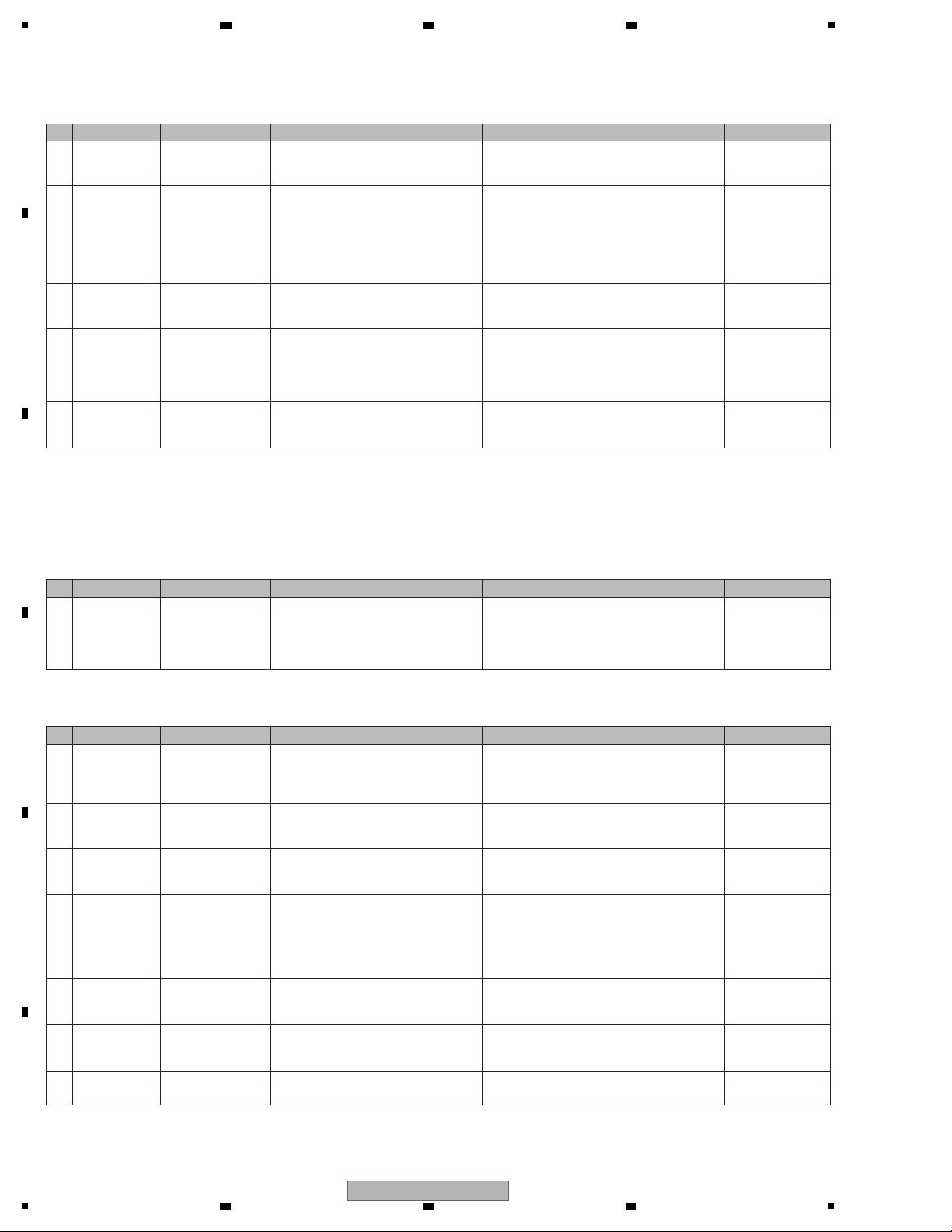
1
1 ————— Traverse mecha Check that focusing is in. (If focusing is
out, tracking close is not possible.)
See “In-focus not possible” above. —————
1 ————— Traverse mecha Check the MAIN DSP (IC301,) using
automatic device diagnostics and the
status LEDs.
If it is judged as NG, the ATAPI drive does not
work properly. If the track data are not output
although loading and rotating are properly
performed, see [6] ATAPI DRIVE. In other cases,
see [9] DRIVE ASSY.
6.1 SERVICE MODE_
[3] Indication of various
information
1 ————— ————— —————
If it is judged as NG, the MAIN DSP (IC302) does
not work properly or communication between the
MAIN CPU (IC10) and MAIN DSP is not
established. Proceed as follows:
—————
2
Power is not
supplied properly.
MAIN Assy Check the power voltages (V+3R3_DSP
and V+1R2_DSP).
The MAIN DSP requires two power supply systems.
Check the connections of the power supply lines.
If soldering is improper, resolder it.
—————
3 The clock is not
properly input.
MAIN Assy Check that the frequency at Pin 38 (DSP_
CLK) of SD_RAM (IC302) is
approx. 129 MHz.
Check the connection of the logic ICs
(IC16, 506).
If soldering is improper, resolder it.
—————
4 The RESET
signal is not
properly input.
MAIN Assy Check that the signals of the DSP_RST
and CPU_DSP_RST lines are H.
Check the connection of the logic IC (IC8).
If soldering is improper, resolder it.
If the signal of the CPU_DSP_RST line is L, the
port on the MAIN CPU may be damaged.
If the signal of the DSP_RST line is L, check the
connection of the logic IC (IC8) and its periphery.
—————
5
Loose connection
between the MAIN
CPU and MAIN DSP
MAIN Assy Check the connection between the
MAIN CPU and MAIN DSP.
Check the connections between MAIN CPU
(IC10) and MAIN DSP (IC301).
If soldering is improper, resolder it.
—————
6
Loose connection
between the MAIN
DSP and SD_RAM
MAIN Assy Check the connection between the
MAIN DSP and SD_RAM.
Check the connections between MAIN DSP
(IC301) and SD_RAM (IC302).
If soldering is improper, resolder it.
—————
No tracking close
2 Signal error SRVB Assy With a CD, check that the E and F signals
fluctuate with 2.2 V at the center.
With a DVD, check the A, B, C, and D
signals.
Check that the signals fluctuate with 2.2 V at the center.
If a DC signal is not output, check the VREF1. If a DC
signal is not output from it, replace the FEP (IC7002).
If an AC signal is not output, check the soldering at the
CN7001–IC7002 of the pickup. If soldering is improper,
resolder it. If soldering is OK, replace the traverse
mecha.
5.4 OPERATIONAL
WAVEFORMS
3 TE signal error SRVB Assy Check that the TE signal fluctuates
with 1.65 V at the center.
Check the connection of the parts at the periphery of
the FEP (IC7002). If soldering is improper, resolder it.
If soldering is OK, replace the FEP (IC7002).
5.4 OPERATIONAL
WAVEFORMS
4 5 6 7 8
4 TEDRV signal
error
SRVB Assy Check that the TEDRV signal fluctuates
with 1.65 V at the center, and that a
pulselike signal is output during tracking
close.
If the output signal waveform is not proper, the connection
of the SODC (IC7006) and its periphery may be
loose or the parts may be defective. If the connection is
loose, reconnect securely. If the connection is OK,
replace the SODC (IC7006).
5.4 OPERATIONAL
WAVEFORMS
6 7 8
[12] Error Codes
[12-1] E-7001: DISC DRIVE ERROR
How to respond when an error code is displayed on the CONTROLLER DISPLAY (LCD) is described below.
The ATAPI drive does not work properly.
[12-2] E-7010: DSP DEVICE ERROR
The MAIN DSP (IC301) does not work properly. Downloading of programs is not possible.
5 ————— ————— If the symptom persists after the above
corrections.
Replace the parts in the order of (1) FEP (IC7002),
(2) SODC (IC7006), (3) DRIVER IC (IC7001),
(4) SRVB Assy, then (5) traverse mecha.
—————
7 ————— ————— If the symptom persists after the above
corrections.
Replace the MAIN Assy. —————
No. Cause Diagnostics Point Item to be Checked Corrective Action Reference
No. Cause Diagnostics Point Item to be Checked Corrective Action Reference
No. Cause Diagnostics Point Item to be Checked Corrective Action Reference
A
2 3 4
B
C
D
E
F
28
CDJ-2000NXS
1
2 3 4
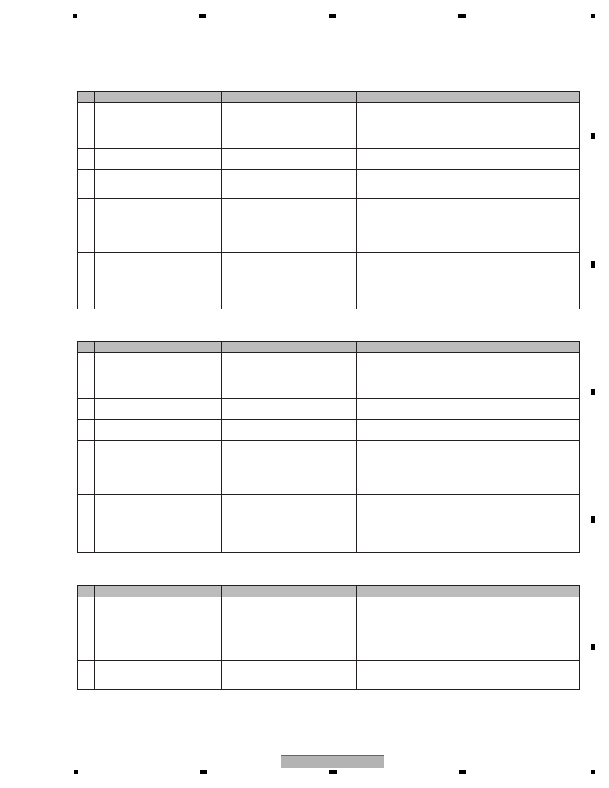
5
1 ————— ————— —————
If it is judged as NG, the USB-B controller (IC701)
does not work properly or communication between
the MAIN CPU (IC10) and USB-B controller is not
established. Proceed as follows: See also “[4-2] No
communication via the USB connector (Type B).”
—————
2 Power is not
supplied properly.
MAIN Assy Check the power voltage of V+3R3_USB_
IO) line.
Check the connections of the power supply lines.
If soldering is improper, resolder it.
—————
2 Power is not
supplied properly.
MAIN Assy Check the power voltages of V+3R3_ETH
and V+3R3A_ETHR) lines.
Check the connections of the power supply lines.
If soldering is improper, resolder it.
—————
3 The clock is not
properly input.
MAIN Assy Check that the frequency at Pin 14
(USB_CLK) of USB-B controller (IC701)
is 48 MHz.
Check the connection of the logic IC (IC4).
If soldering is improper, resolder it.
—————
3 The clock is not
properly input.
MAIN Assy Check that the frequency at Pin 47 (X2) of
PHY CHIP (IC704) is 25 MHz.
Check the connections between X1302 and
PHY CHIP. If soldering is improper, resolder it.
—————
4 The RESET
signal is not
properly input.
MAIN Assy Check that the signals of the USB_RST
and CPU_USB_RST lines are H.
Check the connection of the logic IC (IC8).
If soldering is improper, resolder it.
If the signal of the CPU_USB_RST line is L, the
port on the MAIN CPU may be damaged.
If the signal of the USB_RST line is L, check the
connection of the logic IC (IC8) and its periphery.
—————
4 The RESET
signal is not
properly input.
MAIN Assy Check that the signals of the ETHER_RST
and CPU_ETHER_RST lines are H.
Check the connection of the logic IC (IC8).
If soldering is improper, resolder it.
If the signal of the CPU_ETHER_RST line is L,
the port on the MAIN CPU may be damaged.
If the signal of the ETHER_RST line is L, check the
connection of the logic IC (IC8) and its periphery.
—————
5
Loose connection
between the MAIN
CPU and USB-B
controller
MAIN Assy Check the connection between the MAIN
CPU and USB-B controller.
Check the connections between MAIN CPU
(IC10) and USB-B controller (IC701).
If soldering is improper, resolder it.
—————
5
Loose connection
between the MAIN
CPU and PHY
CHIP controller
MAIN Assy Check the connection between the MAIN
CPU and PHY CHIP controller.
Check the connections between MAIN CPU
(IC10) and PHY CHIP (IC704).
If soldering is improper, resolder it.
—————
[12-3] E-7020: USB-B DEVICE ERROR
The USB-B controller (IC701) does not work properly.
1 ————— ————— ————— If it is judged as NG, the PHY CHIP (IC704) does
not work properly or communication between the
MAIN CPU (IC10) and PHY CHIP is not
established. Proceed as follows: See also
“[5-1] No LAN communication.”
—————
[12-4] E-7021: PHY CHIP ERROR
The PHY CHIP (IC704) does not work properly.
6 ————— ————— If the symptom persists after the above
corrections.
Replace the USB-B controller (IC701). —————
6 ————— ————— If the symptom persists after the above
corrections.
Replace the PHY CHIP (IC704). —————
No. Cause Diagnostics Point Item to be Checked Corrective Action Reference
No. Cause Diagnostics Point Item to be Checked Corrective Action Reference
No. Cause Diagnostics Point Item to be Checked Corrective Action Reference
2
Power is not
supplied properly.
TFTB Assy Check the power voltages of V+3R3T_BF
and V+1R2BF) lines.
The TFT CPU requires two power supply systems.
Check the connections of the power supply lines.
If soldering is improper, resolder it.
—————
1 ————— ————— ————— If it is judged as NG, the TFT CPU (IC4001),
FLASH (IC4004) or SD_RAM (IC4005) does not
work properly or communication between the
MAIN CPU (IC10) and TFT CPU (IC4001) is not
established. Proceed as follows: See also
“[4-2] No communication via the USB connector
(Type B).”
—————
[12-5] E-7023: GUI CPU ERROR
The TFT CPU (IC4001)does not work properly.
6 7 8
A
B
C
D
E
F
CDJ-2000NXS
5
6 7 8
29
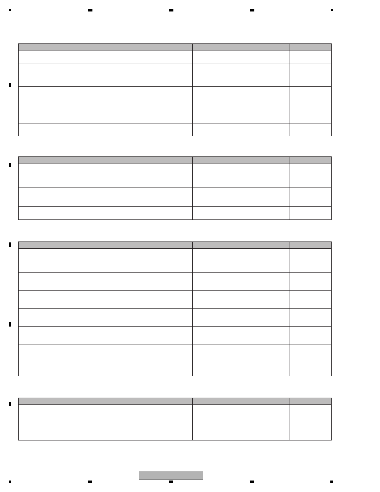
1
2
Power is not
supplied properly.
MAIN Assy Check the power voltages of V+3R3_CPU
and V+1R2_CPU) lines.
The MAIN CPU requires two power supply systems.
Check the connections of the power supply lines.
If soldering is improper, resolder it.
—————
3
Loose connection
between the MAIN
CPU and SD_RAM
MAIN Assy Check the connection between the MAIN
CPU and SD_RAM.
Check the connections between MAIN CPU
(IC10) and SD_RAM (IC108 and IC109).
If soldering is improper, resolder it.
—————
4
Loose connections
in the communication line.
MAIN Assy,
TFTB Assy
Check the connections of communication
line between the MAIN CPU (IC101) and
TFT CPU (IC4001).
If soldering is improper, resolder it. —————
5 The clock is not
properly input.
MAIN Assy Check that the frequency at Pin 38
(CPU_CLKOUT) of SD_RAM (IC108 and
IC109) are approx. 107.9 MHz.
Check the connection of the logic IC (IC10).
If soldering is improper, resolder it.
—————
6
Loose connection
between the MAIN
CPU and SD_RAM
MAIN Assy Check the connection between the MAIN
CPU and SD_RAM.
Check the connections between MAIN CPU
(IC10) and SD_RAM (IC1, 2, 12 and 13).
If soldering is improper, resolder it.
—————
2
Loose connections
in the communication line.
PNLB Assy,
CDCB Assy
Check the connections of communication
line between the PANEL CPU (IC8003)
and CDC (IC5001).
If soldering is improper, resolder it. —————
3 Defective
CDCB Assy
CDCB Assy If the symptom persists after the above
corrections.
Replace the IC5001.
If the symptom persists, replace the CDCB Assy.
—————
3 The clock is not
properly input.
TFTB Assy
Check that the frequency at Pin 38 (BUSCLK)
of SD_RAM (IC4005) is approx. 98 MHz.
Check the connection of the Oscillator (X4002) and
its periphery. If soldering is improper, resolder it.
—————
4 The RESET
signal is not
properly input.
TFTB Assy,
MAIN Assy
Check that the signals of the TFT_RST
line is H.
Check the connection of the logic IC (IC7).
If soldering is improper, resolder it.
If the signal of the TFT_RST line is L, check the
connection of the logic IC (IC7) and its periphery.
—————
5
Loose connection
between the TFT
CPU and FLASH
TFTB Assy Check the connection between the TFT
CPU and FLASH.
Check the connections between TFT CPU
(IC4001) and FLASH (IC4004).
If soldering is improper, resolder it.
—————
6
Loose connection
between the TFT
CPU and SD_RAM
TFTB Assy Check the connection between the TFT
CPU and SD_RAM.
Check the connections between TFT CPU
(IC4001) and SD_RAM (IC4005).
If soldering is improper, resolder it.
—————
1 ————— ————— ————— If it is judged as NG, the CDC (IC5001) does not
work properly or communication between the
PA NEL CPU (IC8003) and CDC (IC5001) is not
established. Proceed as follows:
—————
[12-6] E-7025: CDC DEVICE ERROR
The CDC device (IC5001) for the needle search pad does not work properly.
1 ————— ————— —————
If it is judged as NG, the MAIN CPU (IC10) or SD_RAM
(IC1, 2, 12 and 13) does not work properly or
communication between the MAIN CPU (IC10) and
TFT CPU (IC4001) is not established. Proceed as follows:
—————
[12-7] E-8709: COMMUNICATION ERROR
Communication between the TFT CPU (IC4001) and MAIN CPU (IC10) is not possible.
1
Loose connection
between the MAIN
CPU and
AUTH CHIP
MAIN Assy
Check the connections of communication
line between the MAIN CPU and
AUTH CHIP
.
Check the connections between MAIN CPU
(IC10) and AUTH CHIP (IC14).
If soldering is improper, resolder it.
—————
[12-8] E-7026: AUTH CHIP ERROR
The Apple authentication chip (IC14) for the needle search pad does not work properly.
7 ————— ————— If the symptom persists after the above
corrections.
Replace the TFT CPU (IC4001). —————
7 ————— ————— If the symptom persists after the above
corrections.
Replace the MAIN Assy. —————
2 ————— ————— If the symptom persists after the above
corrections.
Replace the MAIN Assy. —————
No. Cause Diagnostics Point Item to be Checked Corrective Action Reference
No. Cause Diagnostics Point Item to be Checked Corrective Action Reference
No. Cause Diagnostics Point Item to be Checked Corrective Action Reference
No. Cause Diagnostics Point Item to be Checked Corrective Action Reference
A
2 3 4
B
C
D
E
F
30
CDJ-2000NXS
1
2 3 4
 Loading...