

Page 1
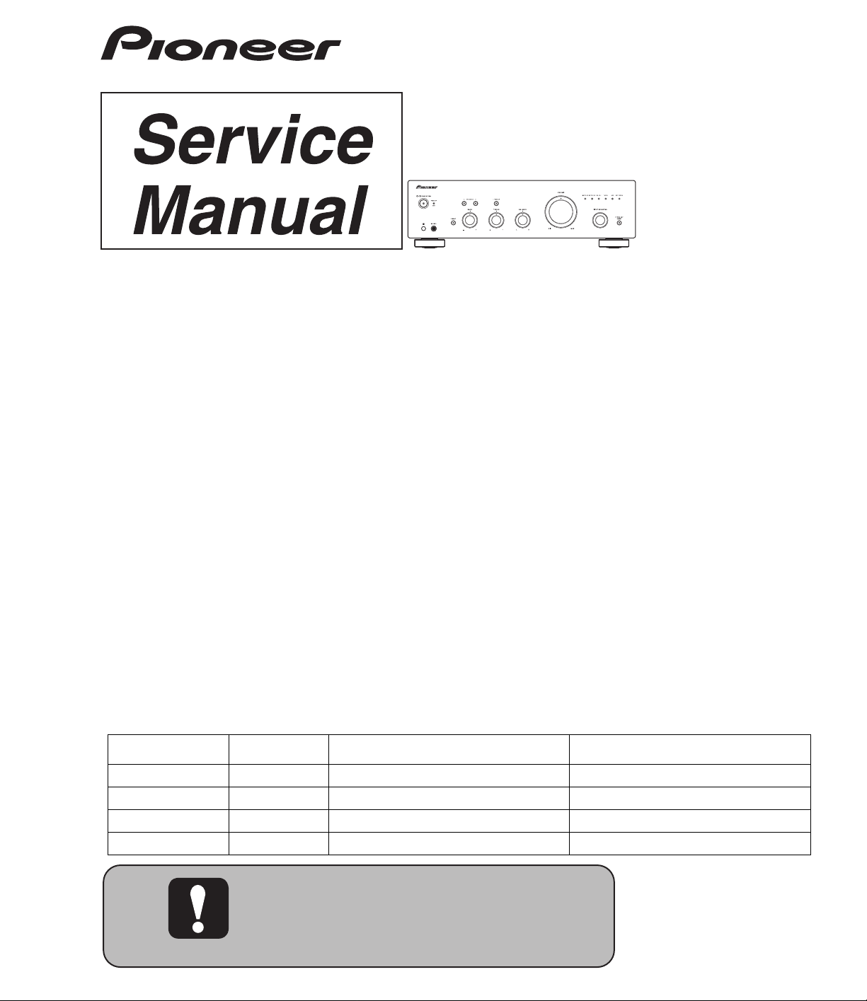
INTEGRATED AMPLIFIER
A-30-K
A-30-S
A-20-K
A-20-S
A-20
ORDER NO.
RRV4297
A-30-K
A-10-K
A-10-S
THIS MANUAL IS APPLICABLE TO THE FOLLOWING MODEL(S) AND TYPE(S).
Model Type Power Requirement Remarks
A-30-K/-S PWSYXE8 AC 220 V to 230 V
A-20-K/-S PWSYXE8 AC 220 V to 230 V
A-20 CUXE AC 120 V
A-10-K/-S SYXE8 AC 220 V to 230 V
Page 2
1
1. SAFETY PRECAUTIONS
The following check should be performed for the
continued protection of the customer and service
technician.
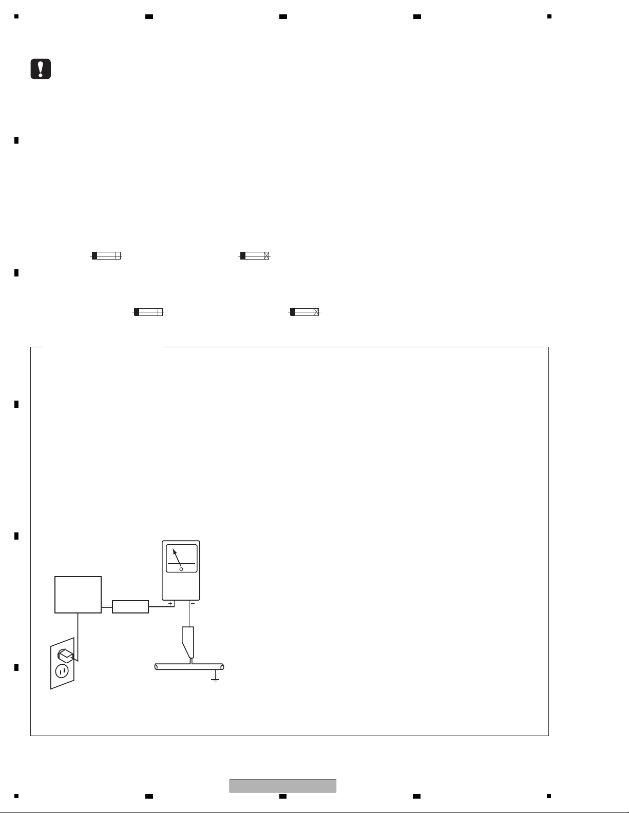
LEAKAGE CURRENT CHECK
Measure leakage current to a known earth ground
(water pipe, conduit, etc.) by connecting a leakage
current tester such as Simpson Model 229-2 or
equivalent between the earth ground and all exposed
metal parts of the appliance (input/output terminals,
screwheads, metal overlays, control shaft, etc.). Plug
the AC line cord of the appliance directly into a 120V
AC 60 Hz outlet and turn the AC power switch on. Any
current measured must not exceed 0.5 mA.
ANY MEASUREMENTS NOT WITHIN THE LIMITS
OUTLINED ABOVE ARE INDICATIVE OF A POTENTIAL
SHOCK HAZARD AND MUST BE CORRECTED BEFORE
RETURNING THE APPLIANCE TO THE CUSTOMER.
2. PRODUCT SAFETY NOTICE
Many electrical and mechanical parts in the appliance
have special safety related characteristics. These are
often not evident from visual inspection nor the protection
afforded by them necessarily can be obtained by using
replacement components rated for voltage, wattage, etc.
Replacement parts which have these special safety
characteristics are identified in this Service Manual.
Electrical components having such features are
identified by marking with a > on the schematics and on
the parts list in this Ser
vice Manua
l.
The use of a substitute replacement component which
does not have the same safety characteristics as the
PIONEER recommended replacement one, shown in the
parts list in this Service Manual, may create shock, fire,
or other hazards.
Product Safety is continuously under review and new
instructions are issued from time to time. For the latest
information, always consult the current PIONEER Service
Manual. A subscription to, or additional copies of,
PIONEER Service Manual may be obtained at a nominal
charge from PIONEER.
Leakage
current
tester
Reading should
not be above
0.5 mA
Device
under
test
Test all
exposed metal
surfaces
Also test with
plug reversed
(Using AC adapter
plug as required)
Earth
ground
AC Leakage T est
(FOR USA MODEL ONLY)
WARNING
This product contains lead in solder and certain electrical parts contain chemicals which are known to the state of California to
cause cancer, birth defects or other reproductive harm.
56 noitisoporP - 6.94252 noitceS edoC ytefaS & htlaeH
NOTICE
(FOR CANADIAN MODEL ONLY)
Fuse symbols (fast operating fuse) and/or (slow operating fuse) on PCB indicate that replacement parts must
be of identical designation.
REMARQUE
(POUR MODÈLE CANADIEN SEULEMENT)
Les symboles de fusible (fusible de type rapide) et/ou (fusible de type lent) sur CCI indiquent que les pièces
de remplacement doivent avoir la même désignation.
This service manual is intended for qualified service technicians ; it is not meant for the casual do-it-
yourselfer. Qualified technicians have the necessary test equipment and tools, and have been trained
to properly and safely repair complex products such as those covered by this manual.
Improperly performed repairs can adversely affect the safety and reliability of the product and may
void the warranty. If you are not qualified to perform the repair of this product properly and safely, you
should not risk trying to do so and refer the repair to a qualified service technician.
2 3 4
SAFETY INFORMATION
A
B
C
D
E
F
2
1
2 3 4
A-30-K
Page 3

5
6 7 8
CONTENTS
SAFETY INFORMATION..........................................................................................................................................................2
1. SERVICE PRECAUTIONS................................................................................... ..... ...... ..... .................................................4
1.1 NOTES ON SOLDERING...............................................................................................................................................4
2. SPECIFICATIONS........................................................ ...... ...... ..... ........................................................................................5
2.1 ACCESSORIES..............................................................................................................................................................5
2.2 SPECIFICATIONS..........................................................................................................................................................5
3. BASIC ITEMS FOR SERVICE ..............................................................................................................................................6
3.1 CHECK POINTS AFTER SERVICING ...........................................................................................................................6
3.2 PCB LOCATIONS...........................................................................................................................................................7
3.3 JIGS LIST.......................................................................................................................................................................7
4. BLOCK DIAGRAM .................................................. ..... ...... ...... ..... ........................................................................................8
4.1 OVERALL CONNECTION DIAGRAM.............................................................................................................................8
4.2 BLOCK DIAGRAM........................................................................................................................................................10
5. DIAGNOSIS ................................................ ...... ...... ..... ............................................. ..........................................................12
5.1 TROUBLESHOOTING..................................................................................................................................................12
5.2 PROTECTION CIRCUIT DESCRIPTION .....................................................................................................................15
5.3 IC INFORMATION........................................................................................................................................................17
6. SERVICE MODE.......................................................... ...... ...... ..... ...... ..... ...........................................................................21
7. DISASSEMBLY ........................................... ...... ...... ..... ...... ...... ...........................................................................................22
8. EACH SETTING AND ADJUSTMENT..................................................... ...... ...... ..... ...... ....................................................29
8.1 HOW TO CHECK THE FIRMWARE VERSION............................................................................................................29
8.2 FARMWARE UPDATING..............................................................................................................................................29
8.3 HOW TO ADJUST THE IDLE CURRENT ....................................................................................................................31
9. EXPLODED VIEWS AND PARTS LIST...............................................................................................................................32
9.1 PACKING SECTION.....................................................................................................................................................32
9.2 EXTERIOR SECTION (A-30/A-20)...............................................................................................................................34
9.3 EXTERIOR SECTION (A-10).......................................................................................................................................38
10. SCHEMATIC DIAGRAM....................................................................................................................................................40
10.1 MAIN ASSY................................................................................................................................................................40
10.2 FRONT ASSY and SECOND POWER SW ASSY (A-30/A-20)..................................................................................42
10.3 MASTER VOLUME ASSY, TONE ASSY and HEADPHONE ASSY ...........................................................................44
11. PCB CONNECTION DIAGRAM........................................................................................................................................46
11.1 MAIN ASSY................................................................................................................................................................46
11.2 FRONT ASSY.............................................................................................................................................................50
11.3 MASTER VOLUME ASSY..........................................................................................................................................52
11.4 TONE ASSY...............................................................................................................................................................53
11.5 HEADPHONE ASSY and SECOND POWER SW ASSY (A-30/A-20)........................................................................54
12. PCB PARTS LIST..............................................................................................................................................................55
A
B
C
D
E
F
A-30-K
5
6 7 8
3
Page 4

1
• For environmental protection, lead-free solder is used on the printed circuit boards mounted in this unit.
Be sure to use lead-free solder and a soldering iron that can meet specifications for use with lead-free solders for repairs
accompanied by reworking of soldering.
• Compared with conventional eutectic solders, lead-free solders have higher melting points, by approximately 40 ºC.
Therefore, for lead-free soldering, the tip temperature of a soldering iron must be set to around 373 ºC in general, although
the temperature depends on the heat capacity of the PC board on which reworking is required and the weight of the tip of
the soldering iron.
Do NOT use a soldering iron whose tip temperature cannot be controlled.
Compared with eutectic solders, lead-free solders have higher bond strengths but slower wetting times and higher melting
temperatures (hard to melt/easy to harden).
The following lead-free solders are available as service parts:
• Parts numbers of lead-free solder:
GYP1006 1.0 in dia.
GYP1007 0.6 in dia.
GYP1008 0.3 in dia.
2 3 4
1. SERVICE PRECAUTIONS
1.1 NOTES ON SOLDERING
A
B
C
D
E
F
4
1
2 3 4
A-30-K
Page 5

5
Remote control unit (A-30-K/-S : CARTA30)
(A-20-K/-S,A-20 : CARTA20)
AAA/R03 dry cell battery x 2 (A-30-K/-S, A-20-K/-S, A-20)
AC Power cord (A-30-K/-S : CJA2B054Z)
(A-20-K/-S, A-10-K/-S : CJA2B020Z)
Warranty card (A-30-K/-S, A-20-K/-S, A-10-K/-S : CQE1A541Z)
Operating instructions (A-30-K/-S, A-20-K/-S, A-10-K/-S : CQX1A1640Y)
(A-20 : CQX1A1644Z)
Amplifier section
Power output specification is for when power supply is 230 V.
(A-30-K/-S, A-20-K/-S, A-10-K/-S)
Power output specification is for when power supply is 120 V.
(A-20)
•Continuous power output (both
channels driven at 20 Hz to 20 kHz)
A-30 . . . . . . . . . . . . . . . . . . . . . . . . . . . . . . . . .70 W + 70 W
A-20, A-10 . . . . . . . . . . . . . . . . . . . . . . . . . . . .50 W + 50 W
(THD 0.1 %, 4 Ω)
A-30 . . . . . . . . . . . . . . . . . . . . . . . . . . . . . . . . . .40 W+40 W
A-20, A-10 . . . . . . . . . . . . . . . . . . . . . . . . . . . . .30 W+30 W
(THD 0.05 %, 8 Ω)
Audio section
•Input (Sensitivity/Impedance)
SACD/CD, NETWORK, TUNER, AUX, RECORDER
. . . . . . . . . . . . . . . . . . . . . . . . . . . . . . . . . . . 200 mV/50 kΩ
POWER AMP DIRECT (A-30 only). . . . . . . . . . . . .1 V/10 kΩ
PHONO (MM). . . . . . . . . . . . . . . . . . . . . . . . . 2.8 mV/50 kΩ
•Output (Level/Impedance)
RECORDER OUT . . . . . . . . . . . . . . . . . . . . . 200 mV/2.2 kΩ
PHONES . . . . . . . . . . . . . . . . . . . . . . . . . . . . . 250 mV/32 Ω
•Frequency response
SACD/CD, NETWORK, TUNER, AUX, RECORDER
. . . . . . . . . . . . . . . . . . . . . . . . . . . . . 5 Hz to 100 kHz dB*
PHONO (MM). . . . . . . . . . . . . . . .20 Hz to 20 kHz ±0.5 dB*
* Measured with DIRECT button switched on.
•Tone control
(When VOLUME is set to
-
30 dB)
Bass. . . . . . . . . . . . . . . . . . . . . . . . . . . . . .± 10 dB (100 Hz)
Treble. . . . . . . . . . . . . . . . . . . . . . . . . . . . .± 10 dB (10 kHz)
•Signal-to-Noise Ratio (IHF SHORTED,
A-NETWORK)
SACD/CD, NETWORK, TUNER, AUX, RECORDER
. . . . . . . . . . . . . . . . . . . . . . . . . . . . . . . . . . . . . . . . 105 dB*
PHONO (MM, 2.8 mV input) . . . . . . . . . . . . . . . . . . .77 dB*
* Measured with DIRECT button switched on.
•Speaker load impedance
A, B . . . . . . . . . . . . . . . . . . . . . . . . . . . . . . . . . 4 Ω to 16 Ω
A+B. . . . . . . . . . . . . . . . . . . . . . . . . . . . . . . . . . 8 Ω to 32 Ω
Bi-wiring . . . . . . . . . . . . . . . . . . . . . . . . . . . . . . 4 Ω to 16 Ω
Miscellaneous
Power requirements
. . . . . . . . . . . . . . . . . . . . . . . . . . AC 220 V to 230 V, 50 Hz
(A-30-K/-S, A-20-K/-S, A-10-K/-S)
. . . . . . . . . . . . . . . . . . . . . . . . . . . . . . . . . . AC 120 V, 60 Hz
(A-20)
Power consumption
A-30 . . . . . . . . . . . . . . . . . . . . . . . . . . . . . . . . . . . . . . 175 W
A-20/A-10. . . . . . . . . . . . . . . . . . . . . . . . . . . . . . . . . . 135 W
In standby . . . . . . . . . . . . . . . . . . . . . . . . . . . . . . . . . 0.3 W
Dimensions
. . . . . . . . . . . . . . .435 mm (W) x 128 mm (H) x 360 mm (D)
Weight (without package)
A-30 . . . . . . . . . . . . . . . . . . . . . . . . . . . . . . . . . . . . . . 7.9 kg
A-20 . . . . . . . . . . . . . . . . . . . . . . . . . . . . . . . . . . . . . . 7.2 kg
A-10 . . . . . . . . . . . . . . . . . . . . . . . . . . . . . . . . . . . . . . 6.7 kg
Note
•Specifications and the design are subject to
possible modifications without notice, due to
improvements.
•Corporation and product names mentioned herein
are trademarks or registered trademarks of the
respective corporations.
2. SPECIFICATIONS
2.1 ACCESSORIES
6 7 8
A
2.2 SPECIFICATIONS
B
C
D
5
A-30-K
6 7 8
E
F
5
Page 6
1
Item to be checked regarding audio
Distortion
Noise
Volume too low
Volume too high
Volume fluctuating
Sound interrupted
To keep the product quality after servicing, confirm recommended check points shown below.
See the table below for the items to be checked regarding audio.
No. Procedures Check points
1
Check the symptom pointed out by a customer The pointed content should not reoccur
Sound and operation should not be defective
2
Check each input and main VOL (check the
operation of selector)
The sound is output by selecting an analog-connected input
with a selector and the sound volume should change by
rotating main VOL knob
3
Check the tone control, balance, and function The sound quality or right and left balances should change
by rotating each V OL knob
4
Check LOUDNESS and DIRECT functions The sound quality should change by setting LOUDNESS
function to ON. LOUDNESS function should be disabled by
setting DIRECT function to ON.
5
Check POWER AMP DIRECT terminal (only A-30)
(connected from pre-out terminal of AV AMP to
POWER AMP DIRECT terminal)
The sound volume should change by adjusting the sound
volume of connected AV AMP. The sound volum e shoul d not
be changed by the main VOL on the main unit.
6 Check SPEAKER A/B and headphone terminal There should not be defect in sound such as noise
7
Check the external package Check scratch or taint is not generated after accept ing the
repair
2 3 4
3. BASIC ITEMS FOR SERVICE
3.1 CHECK POINTS AFTER SERVICING
A
B
C
D
E
F
6
1
2 3 4
A-30-K
Page 7
5
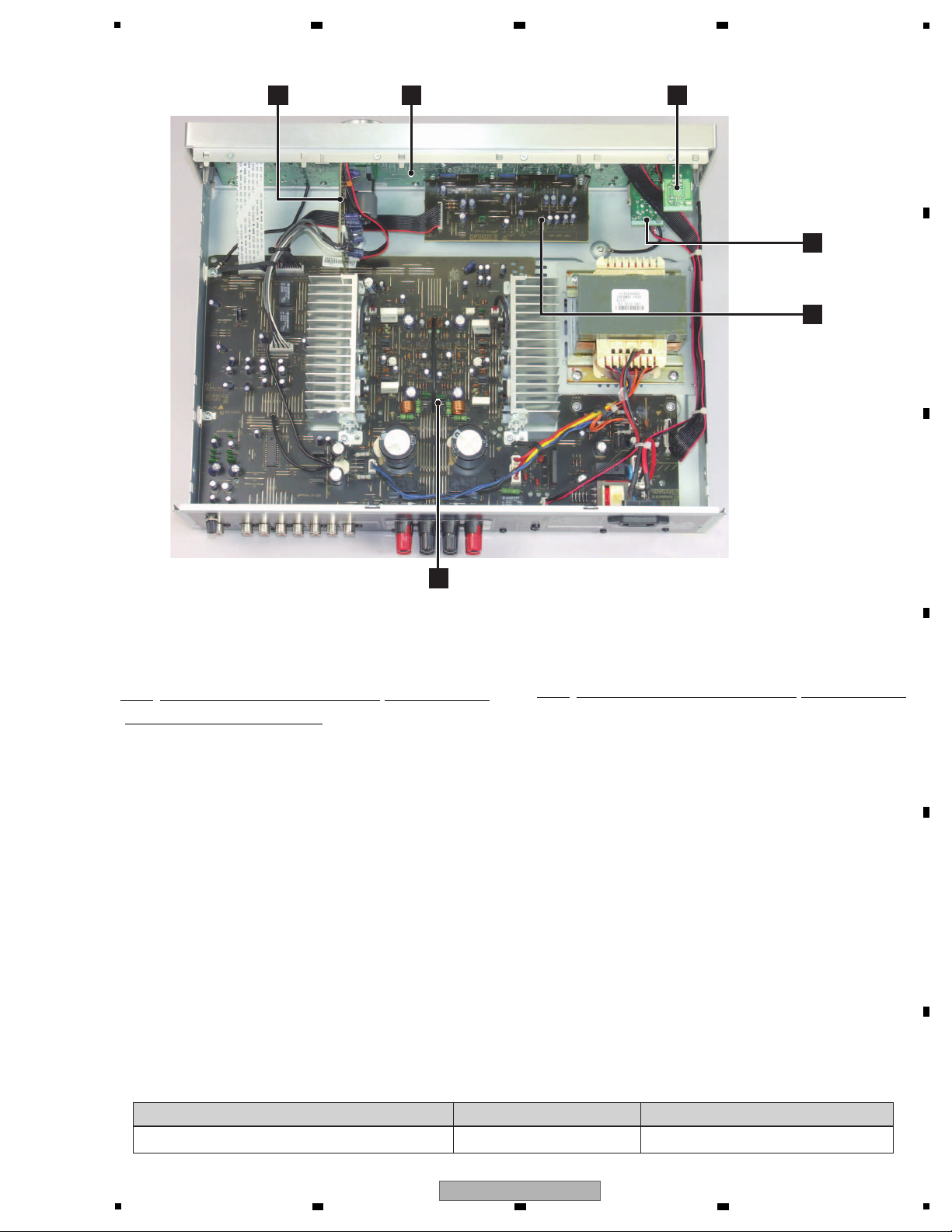
SECOND POWER SW ASSY
MAIN ASSY
A
MASTER VOLUME ASSY
C F
HEADPHONE ASSY
E
TONE ASSY
D
FRONT ASSY
B
NOTES: - Parts marked by “NSP” are generally unavailable because they are not in our Master Spare Parts List.
-
The > mark found on some component parts indicates the importance of the safety factor of the part.
Therefore, when replacing, be sure to use parts of identical designation.
Name Jig No. Remarks
UPDATE JIG GGF1675 Farmware Update
3.2 PCB LOCATIONS
6 7 8
A
B
Mark No. Description Part No.
LIST OF ASSEMBLIES
NSP 1..MAIN ASSY (A-30-K/-S) COP12421B
2..MAIN ASSY AZW7487
NSP 1..MAIN ASSY (A-20-K/-S) COP12421D
2..MAIN ASSY AZW7489
NSP 1..MAIN ASSY (A-20) COP12421E
2..MAIN ASSY AZW7490
NSP 1..MAIN ASSY (A-10-K/-S) COP12421F
2..MAIN ASSY AZW7491
NSP 1..FRONT ASSY (A-30-K/-S) COP12422B
2..FRONT ASSY AZW7482
2..MASTER VOLUME ASSY AZW7476
2..TONE ASSY AZW7477
2..HEADPHONE ASSY AZW7479
2..SECOND POWER SW ASSY AZW7478
Mark No. Description Part No.
NSP 1..FRONT ASSY (A-20-K/-S) COP12422C
2..FRONT ASSY AZW7483
2..MASTER V OLU ME ASSY AZW7481
2..TONE ASSY AZW7477
2..HEADPHONE ASSY AZW7479
2..SECOND POWER SW ASSY AZW7478
NSP 1..FRONT ASSY (A-20) COP12422G
2..FRONT ASSY AZW7484
2..MASTER V OLU ME ASSY AZW7481
2..TONE ASSY AZW7477
2..HEADPHONE ASSY AZW7479
2..SECOND POWER SW ASSY AZW7478
NSP 1..FRONT ASSY (A-10-K/-S) COP12422D
2..FRONT ASSY AZW7485
2..MASTER V OLU ME ASSY AZW7481
2..TONE ASSY AZW7477
2..HEADPHONE ASSY AZW7479
C
D
E
3.3 JIGS LIST
5
6 7 8
A-30-K
F
7
Page 8
1
MAIN AS
(A-30-K/
(A-20-K/
(A-20
(A-10-K/
A
FRONT ASSY
(A-30-K/-S : AZW748
(A-20-K/-S : AZW748
(A-20 : AZW748
(A-10-K/-S : AZW748
B
SECOND POWER SW ASSY
(A-30-K/-S, A-20-K/-S, A-20 : AZW7478)
F
C
TONE ASSY
(AZW7477)
D
HEADPHONE ASSY
(AZW7479)
E
2 3 4
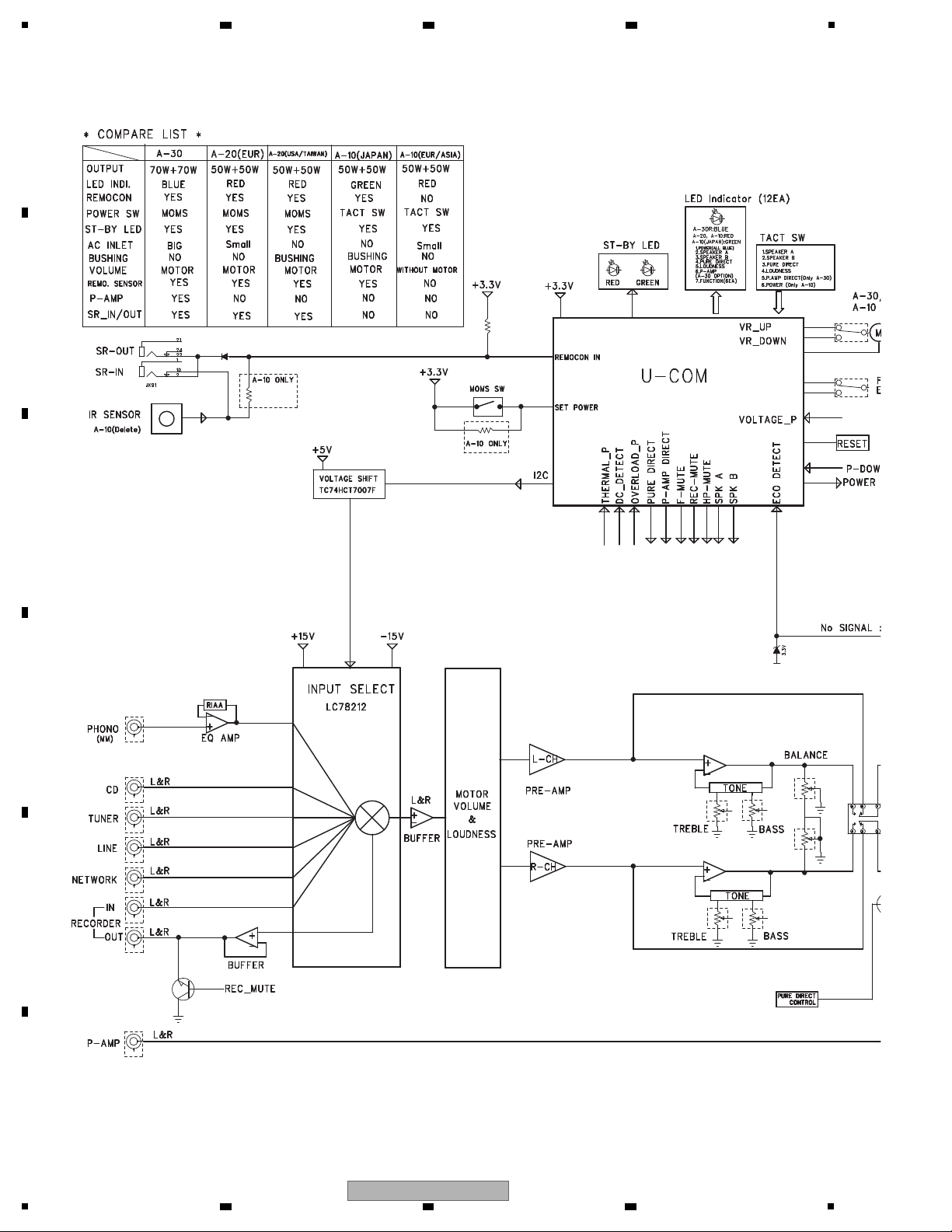
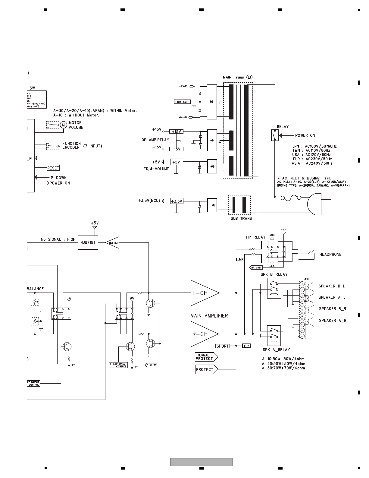
4. BLOCK DIAGRAM
4.1 OVERALL CONNECTION DIAGRAM
A
B
C
D
E
F
8
1
2 3 4
A-30-K
Page 9
5
MAIN ASSY
(A-30-K/-S : AZW7487)
(A-20-K/-S : AZW7489)
(A-20 : AZW7490)
(A-10-K/-S : AZW7491)
S : AZW7482)
S : AZW7483)
: AZW7484)
S : AZW7485)
MASTER VOLUME ASSY
(A-30-K/-S : AZW7476)
(A-20-K/-S, A-20,
A-10-K/-S : AZW7481)
C
Therefore, when replacing, be sure to use parts of identical designation.
When ordering service parts, be sure to refer to "EXPLODED VIEWS and PARTS LIST" or "PCB PARTS LIST".
The > mark found on some component parts indicates the importance of the safety factor of the part.
6 7 8
A
B
C
D
E
5
6 7 8
A-30-K
F
9
Page 10
1
4.2 BLOCK DIAGRAM
A
B
2 3 4
C
D
E
F
10
1
2 3 4
A-30-K
Page 11
5
6 7 8
A
B
C
D
E
F
A-30-K
5
6 7 8
11
Page 12
1
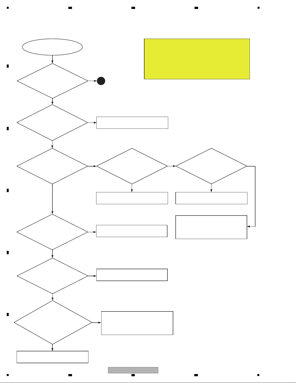
Is the Power supply
turned ON ?
A
No
No
Yes
Yes
No No No
Yes Yes
Yes
Yes
Yes
Yes
No
No
No
[Status of product]
Insert AC Power cord
Main unit POWER SW: ON (A-30/A-20)
POWER ON operation by remote control Unit
Select SPEAKER-A
INPUT : SACD/CD
Is the standby LED blinking ?
No sound
The protection circuit is operating
Is the voltage of ST_+3.3V
(CN94: 4, 5 pins) +3.3V ?
Is the voltage of IC91: 2 pin
approximately 5V ?
Is there AC waveform on
D913 anode side ?
IC91 failure
D913 failure
D914 failure
Is BACK UP line set to "H" ?
(CN94: 7 pin)
Q903, D917 failure
F901 failure
T901 failure
Is voltage of IC11: 1 pin +3.3V ?
IC12 failure
Is there
a waveform of Remote
Controller signal at IC11: 59 pin
(REMOTE IN) when POWER key
on the Remote Control
Unit pressed ?
IC11 failure
RC11 failure
Connection failure between BN94
and CN94(A-30/A-20)
(For the type, refer to the 5.2 PROTECTION CIRCUIT DESCRIPTION)
No sound
5. DIAGNOSIS
5.1 TROUBLESHOOTING
A
2 3 4
B
C
D
E
F
12
1
2 3 4
A-30-K
Page 13
A
No
No
No
No
No
No No No
B
Yes
Yes
Yes
Yes
Yes
Yes
Yes Yes
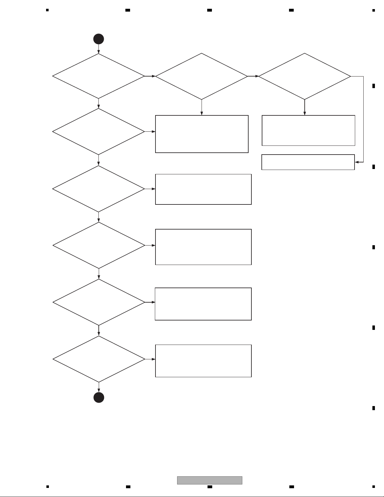
Does the protection
relay "click" and is it turned ON
after the power supply
is turned ON ?
Is IC11: 50 pin
(SPEAKER A) set to "H" ?
Is SPEAKER A LED
lighting ?
Is there output at
HP terminal ?
Relay power supply resistance
(R392, R394) failure
RY33 failure
Connection failure between
CY93 and CX93
S103 failure
IC11 failure
IC11 failure
Is there output at
REC OUT terminal ?
IC21 failure, communication failure
Connection failure between
CY93 and CX93
Solder failure of input pin jack
Is there a signal at
BN51:1, 9 pins ?
IC23 failure
Solder failure of IC23 I/O coupling
electrolysis capacitor
Connection failure between
CN51 and BN51
Is there a signal at
BN51:3, 7 pins ?
IC41 failure
Solder failure of IC41 I/O coupling
electrolysis capacitor
Check IC42 power supply (±7.5V)
Is there a signal at
BN51:3, 7 pins ?
IC41 failure
Solder failure of IC41 I/O coupling
electrolysis capacitor
Check IC42 power supply (±7.5V)
5
6 7 8
A
B
C
D
E
F
A-30-K
5
6 7 8
13
Page 14
1
A-30 ONLY
B
Yes
Yes
No
Yes
No
No
No
No
Yes
Yes Yes Yes
No
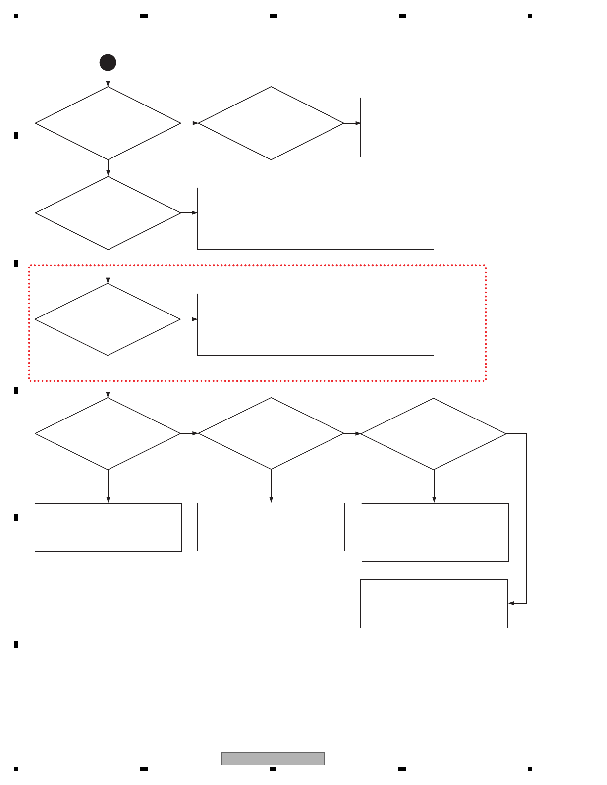
Isn't the
symptom changed by
DIRECT ON/OFF ?
Only DIRECT OFF
is not output
Solder failure of R503, R514
Connection failure between
CN41 and BN41
IC51, IC52 failure
Is there
a signal at J208 and
J209 (RY21 output) ?
PURE DIRECT control signal circuit
failure (Q203, Q204, R259, R261)
Connection failure between CY93 and CX93
RY21 failure
Is there
a signal at J215
(RY22 output) ?
P_AMP DIRECT control signal circuit
failure (Q205, Q206, R260, R262)
Connection failure between CY93 and CX93
RY22 failure
Is there a
signal at power amplifier
input (R301, R302) ?
Isn't F_MUTE
set to "H" ?
(Isn't the sound
muted ?)
Is ±15V of
MUTE circuit properly
supplied ?
Solder failure of R301,
R302, C301, C302
Reset MUTE
Solder failure of IC11:
44 pin
F_MUTE control signal
circuit failure (Q207-Q212)
Connection failure
between CY93 and CX93
D250 failure
Solder failure of R275
A
2 3 4
B
C
D
E
F
14
1
2 3 4
A-30-K
Page 15

5
1. PROTECTION operation
Purpose of PROTECTION operation
Protection of operation due to failure of product
Protection of operation due to wrong use by a user
e.g.) Rare short of speaker connection is generated, or product is installed by
blocking the heat release hole
1.1 DC DETECT
After DC DETECT is detected, MUTE ON & PROTECTION RELAY OFF are carried out.
If DC DETECT is detected for 3 seconds or more continuously, it is evaluated as "1.1.1 AMP failure" shown below.
If DC DETECT is detected for less than 3 seconds, it is evaluated as 1.1.2 SIGNAL CLIP" shown below.
1.1.1 AMP failure
If DC DETECT is detected for 3 seconds or more continuously, it is evaluated as "AMP failure" and
the power is turned OFF.
If the power supply is automatically turned OFF after AMP failure is detected, all key operations are prohibited
(power ON is prohibited).
For turn ON the power supply again, refer to "3. How to reset the prohibition of power ON" shown below.
1.1.2 SIGNAL CLIP
If DC DETECT is detected for less than 3 seconds, it is evaluated as "SIGNAL CLIP".
If the detection of DC DETECT is reset within 3 seconds, MUTE OFF & PROTECTION RELAY ON
are carried out.
NOTE) If the detection of DC DETECT is reset within 3 seconds and DC detection functions immediately,
PROTECTION RELAY OFF/ON is repeated, however, there is no problem.
1.2 OVER LOAD
MUTE ON & PROTECTION RELAY OFF are carried out immediately after the detection and the power is
turned OFF.
After OVER LOAD is detected, the key operation is not prohibited (the power supply can be turned ON).
NOTE) If a short of speaker cable may be generated, the connection is made again and the power supply
cannot be turned ON by a user, so a complaint is generated.
If AMP is broken actually, DC detection operates, so there is no problem.
1.3 Temperature PROTECTION
MUTE ON & PROTECTION RELAY OFF are carried out immediately after the detection and the power is
turned OFF.
After temperature PROTECTION is detected, the key operation is not prohibited (the power supply
can be turned ON).
NOTE) After the detection, if the temperature is still high even by turning ON the power supply,
the temperature PROTECTION is detected again and the power supply is turned OFF.
1.4 Power PROTECTION
MUTE ON & PROTECTION RELAY OFF are carried out immediately after the detection and the power is
turned OFF.
If the power supply is automatically turned OFF after the power PROTECTION is detected, all key operations are
prohibited (power ON is prohibited).
For turn ON the power supply again, refer to "3. How to reset the prohibition of power ON" shown below.
2. Keeping the prohibition of power ON after 1.1.1 AMP failure is detected and 1.4 power
PROTECTION is detected
If the power supply is automatically turned OFF after AMP failure is detected and power PROTECTION is detected,
all key operations are prohibited (power ON is prohibited).
The power ON prohibition status is kept even if the backup is carried out and the power cord is disconnected and
inserted.
For turn ON the power supply again, refer to "3. How to reset the prohibition of power ON" shown below.
5.2 PROTECTION CIRCUIT DESCRIPTION
6 7 8
A
B
C
5
6 7 8
A-30-K
D
E
F
15
Page 16
1
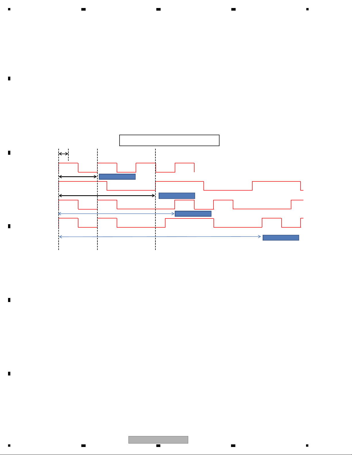
200ms
On
Temperature
Protection
Off
AMP Overload
Protection
1CYCLE : 1.4S
DC DETECT
(DC Balance)
Power
Protection
1TIME : 800mS
1TIME : 2.4S
1TIME: 4.2S
1TIME : 2S
Protect LED display specifications
3. How to reset the prohibition of power ON
Press Front Key [ DIRECT ] + [ SPEAKER B ] at the same time for 2 seconds or more continuously.
The key prohibition mode after 1.1.1 AMP failure is detected and 1.4. power PROTECTION is detected is released and
the power supply is turned ON.
4. STANDBY LED display after PROTECTION is detected
Each PROTECTION operations above are identified by blinking timing of STANDBY LED.
The blinking of LED is continued until the power supply is turned ON again.
For the blinking specification of LED, refer to "Protect LED display specifications" shown below.
A
B
2 3 4
C
D
E
F
16
1
2 3 4
A-30-K
Page 17
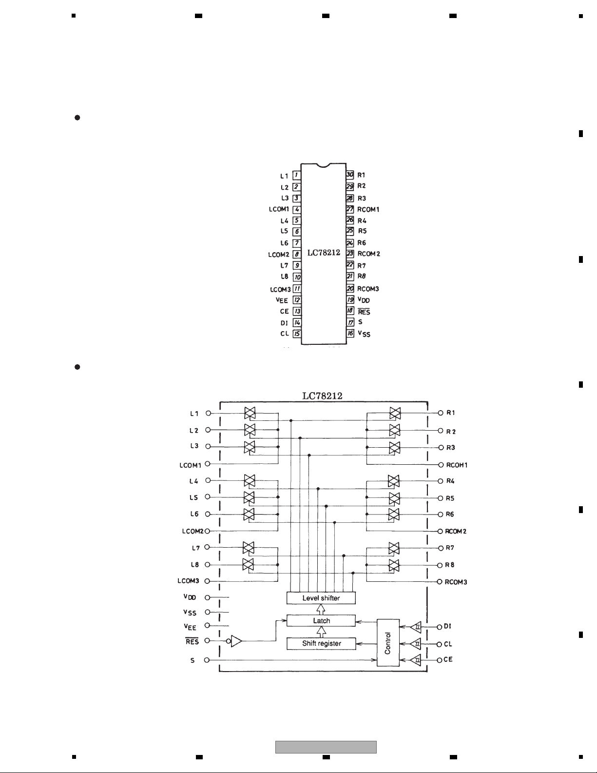
5
1/1
HVILC78212
(Analog Function Switch)
(Top View)
Pin Layout
Block Diagram
5.3 IC INFORMATION
6 7 8
A
B
C
D
E
F
A-30-K
5
6 7 8
17
Page 18
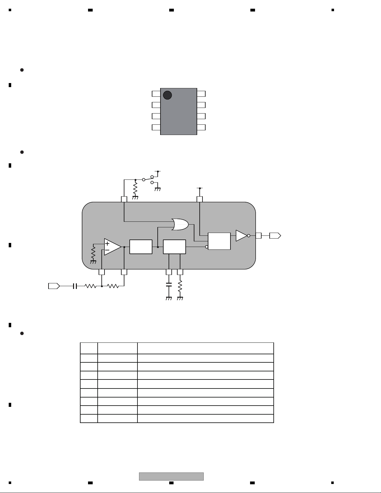
1
1/1
CVINJU7181RB1
(Signal Level Sensor System)
(TVSP8)
Level
Detector
Delay
Latch
CLR
D
L
IN
OUT
V
+
V
+
ON
OFF
External Trigger
18
54
Pin Layout
Block Diagram
Pin Function
(Top View)
1 IN AC Input
2 AMP_OUT Amplifier Output
3 TRIN External Trigger Input
4 GND Ground
5 CAP_D Capacitor connection terminal for delay time setting
6 RES_D Resister connection terminal for delay time setting
7 OUT DC Output
8 V
+
Power Supply Voltage
FunctionPin NameNo.
A
2 3 4
B
C
D
E
F
18
1
A-30-K
2 3 4
Page 19

1/3
CVIANAM1656A
(Micro Controller)
V
REF-
AIN10/PF0
AIN7/PB7
AIN6/PB6
[I2C_SDA] AIN5/PB5
[I2C_SCL] AIN4/PB4
[TIM1_ETR] AIN3/PB3
[TIM1_CH3N] AIN2/PB2
[TIM1_CH2N] AIN1/PB1
[TIM1_CH1N] AIN0/PB0
AIN8/PE7
AIN9/PE6
AIN11/PF3
V
REF+
V
DDA
V
SSA
6463 6261 6059 5857565554 5352 5150 49
48
47
46
45
44
43
42
41
40
39
38
37
36
35
34
33
171819 202122 2324 2930 31322526 2728
1
2
3
4
5
6
7
8
9
10
11
12
13
14
15
16
V
SS
VCAP
V
DD
V
DDIO_1
[TIM3_CH1] TIM2_CH3/PA3
UART1_RX/ (HS) PA4
UART1_TX/ (HS) PA5
UART1_CK/ (HS) PA6
AIN15/PF7
AIN14/PF6
AIN13/PF5
AIN12/PF4
NRST
OSCIN/PA1
OSCOUT/PA2
V
SSIO_1
PG1/CAN_RX
PG0/CAN_TX
PC7 (HS)/SPI_MISO
PC6 (HS)/SPI_MOSI
V
DDIO_2
V
SSIO_2
PC5 (HS)/SPI_SCK
PC4 (HS)/TIM1_CH4
PC3 (HS)/TIM1_CH3
PC2 (HS)/TIM1_CH2
PC1 (HS)/TIM1_CH1
PE5/SPI_NSS
PI0
PG4
PG3
PG2
PD3 (HS)/TIM2_CH2[ADC_ETR]
PD2 (HS)/TIM3_CH1[TIM2_CH3]
PD1 (HS)/SWIM
PD0 (HS)/TIM3_CH2 [TIM1_BKIN] [CLK_CCO]
PE0 (HS)/CLK_CCO
PE1 (T)/I2C_SCL
PE2 (T)/I2C_SDA
PE3/TIM1_BKIN
PE4
PG7
PG6
PG5
PD7/TLI [TIM1_CH4]
PD6/UART3_RX
PD5/UART3_TX
PD4 (HS)/TIM2_CH1 [BEEP]
Pin Layout
1. (HS) high sink capability.
2. (T) True open drain (P-buffer and protection diode to VDD not implemented).
3. [ ] alternate function remapping option (If the same alternate function is shown twice, it indicates an exclusive choice not a
duplication of the function).
4. CAN_RX and CAN_TX is available on STM8S208xx devices only.
5
6 7 8
A
B
C
D
E
5
6 7 8
A-30-K
F
19
Page 20

A
2/3
CVIANAM1656A
(Micro Controller)
Block Diagram
XTAL 1-24 MHz
RC int. 16 MHz
RC int. 128 kHz
STM8 core
Debug/SWIM
I
2
C
SPI
UART1
UART3
AWU timer
Reset block
Reset
POR
BOR
Clock controller
Detector
Clock to peripherals and core
10 Mbit/s
LIN master
16 channels
Address and data bus
Window WDG
Up to 128 Kbytes
Up to 2 Kbytes
Up to 6 Kbytes
Boot ROM
ADC2
beCAN
Reset
400 Kbit/s
1 Mbit/s
Master/slave
Single wire
autosynchro
debug interf.
SPI emul.
high density program
Flash
data EEPROM
RAM
16-bit general purpose
16-bit advanced control
timer (TIM1)
timers (TIM2, TIM3)
8-bit basic timer
(TIM4)
Beeper
1/2/4 kHz
beep
Independent WDG
4 CAPCOM
channels
Up to
5 CAPCOM
channels
Up to
+ 3 complementary
outputs
B
1
2 3 4
C
D
E
F
20
A-30-K
1
2 3 4
Page 21

5
6 7 8
3/3
CVIANAM1656A
Pin Function
(Micro Controller)
Pins Pin Name TYPE
1 NRST I/O
2 PA1/OSCIN I/O OSC_IN GPIO O L L - OSC_IN
3 PA2/OSCOUT I/O OSC_OUT GPIO O L L - OSC_OUT
4 Vssio_1 S
5 Vss S
6 Vcap S
7 Vdd S
8 Vddio_1 S
9 PA3/TIM2_CH3 I/O PA3 TIM2_CH3 I - - H SEC_POWER
10 PA4/UART1_Rx I/O PA4 UART1 I/O - L - UPDATE_TX
11 PA5/UART1_Tx I/O PA5 UART1 O H L L UPDATE_RX
12 PA6/UART1_Clk I/O PA6 UART1 I - - H ECO_DETECT
13 PF7/AN15 I/O PF7 ADC O L L L STBY_LED
14 PF6/AN14 I/O PF6 ADC O L L H LOUDNESS_LED
15 PF5/AN13 I/O PF5 ADC O L L H SPEAKER_B_LED
16 PF4/AN12 I/O PF4 ADC O L L H SPEAKER_A_LED
17 PF3/AN11 I/O PF3 ADC O L L H P_AMP_DIRECT
18 Vref+ S
19 Vdda S
20 Vssa S
21 Vref- S
22 PF0/AN10 I/O PF0 ADC O L L H P_AMP LED
23 PB7/AN7 I/O PB7 ADC O L L H PHONO_LED
24 PB6/AN6 I/O PB6 ADC I - - H MODEL_OPT
25 PB5/AN5 I/O PB5 ADC O L L H TUNER_LED
26 PB4/AN4 I/O PB4 ADC O L L H RECORDER_LED
27 PB3/AN3 I/O PB3 ADC O L L H AUX_LED
28 PB2/AN2 I/O PB2 ADC O L L H NETWORK_LED
29 PB1/AN1 I/O PB1 ADC O - - - KEY_IN#2
30 PB0/AN0 I/O PB0 ADC O - - - KEY_IN#1
31 PE7/AN8 I/O PE7 ADC O L L H CD_LED
32 PE6/AN9 I/O PE6 ADC O L L H VR_DOWN
33 PE5/SPI_NSS I/O PE5 SPI O L L H FUNC_CE
34 PC1/TIM1_CH1 I/O PC1 TIM1_CH1 O L L H VR_UP
35 PC2/TIM1_CH2 I/O PC2 TIM1_CH2 I - - L THERMAL_P
36 PC3 I/O PC3
37 PC4/TIM1_CH4 I/O PC4 TIM1_CH4 I - - L OVERLOAD_P
38 PC5/SPI_SCK I/O PC5 SPI O L L H/L FUNC_CLK
39 Vssio_2 S
40 Vddio_2 S
41 PC6/SPI_MOSI I/O PC6 SPI O L L H/L FUNC_DATA
42 PC7/SPI_MISO I/O PC7 SPI I - - L VOLTAGE_P
43 PG0/CAN_Tx I/O PG0 O H H(OD) H REC_MUTE
44 PG1/CAN_Rx I/O PG1 O H H(OD) H F_MUTE
45 PG2 I/O PG2 O L L H P_ON_RELAY
46 PG3 I/O PG3
47 PG4 I/O PG4 O L L H PURE_DIRECT
48 PI0 I/O PI0 O L L 49 PG5 I/O PG5 O L L H SPEAKER_B
50 PG6 I/O PG6 O L L H SPEAKER_A
51 PG7 I/O PG7 O L L H PURE_DIRECT_LED
52 PE4 I/O PE4 I - - H/L FUNCTION_EN1
53 PE3/TIM1_BKIN I/O PE3 TIM1_BKIN I - - H/L FUNCTION_EN2
54 PE2/I2C_SDA I/O PE2 I2C I - - L UPDATE_SEL
55 PE1/I2C_SCL I/O PE1 I2C O L L 56 PE0/CLK_CCO I/O PE0 CLK_CCO O L L H POWER_LED
57 PD0/TIM3_CH2 I/O PD0 TIM3_CH2 O L L H APD_LED
58 PD1/SWIM I/O DEBUG GPIO O
59 PD2/TIM3_CH1 I/O PD2 TIM3_CH1 I - - H/L REMOTE_IN
60 PD3/TIM2_CH2 I/O PD3 TIM2_CH2 O L L H DIMMER
61 PD4/TIM2_CH1 I/O PD4 TIM2_CH1 O L L 62 PD5/UART3_Tx I/O PD5 UART3 O L L 63 PD6/UART3_Rx I/O PD6 UART3 O L L L HP_MUTE
64 PD7/TLI I/O PD7 TLI O - - L BACK_UP
Main
Function
(After reset)
Default
Alternate
functions
USE
I - - L DC_DETECT
O L L H LOUDNESS
- - - NRST
- - - VSSIO_1
- - - VSS
- - - VCAP
- - - VDD
- - - VDDIO1
- - -
- - -
- - -
- - -
Status
init stby Act.Lvl
Pin Description
Debug Jig
A
B
C
D
E
6. SERVICE MODE
There is no information to be shown in this chapter.
5
6 7 8
A-30-K
F
21
Page 22

1
1
1
1
3
4
1
2
2
2
2
2
Top Cabinet
Note 1 : Even if the unit shown in the photos and illustrations in this manual may differ from your product, the procedures
described here are common.
Note 2 : As for the assembling, please perform assembling following to the opposite procedures of How to Disassemble.
If any notes are existed, please follow those instructions.
Note 3 : Before starting the diagnosis, wait for several seconds until the electricity of the unit is discharged.
While spreading
Top Cabinet
Rear Panel
Insert nails
While spreading
[1] Top Cabinet
(1) Remove the four screws.
(
A-30-K, A-20-K, A-20, A-10-K: )
CTB4+6FFZRP
(
A-30- S, A-20-S, A-10-S:
)
CTB4+6FFCP
(2) Remove the five screws.
(BBZ30P060FTB)
(3) Insert nails between the Top Cabinet and
Rear Panel and pull the Top Cabinet
backward horizontally.
(4) Take out Top Cabinet upward while spreading
Rear Side Piece.
2 3 4
7. DISASSEMBLY
A
B
C
D
E
F
22
1
2 3 4
A-30-K
Page 23

1
2
3
3
2
HEADPHONE ASSY
MAIN ASSY
Bottom Chassis
CN94
CN55
Ground Cable from the HEADPHONE ASSY
[2] Diagnosis
[3] Front Section
(1) Remove the screw. (CTW3+6JR)
(2) Cut the two Clampers. (CHR301)
(3) Disconnect the two connectors.
5
6 7 8
A
B
C
D
E
F
A-30-K
5
6 7 8
23
Page 24

1
5
4
MAIN ASSY
Wire Clamper
4
4
CN51
CN41
CY93
Front Section
Ground Cable
from the FRONT ASSY
6
6
6
6
6
6
7
7
(4) Disconnect the three connectors.
(5) Remove the screw. (CTW3+6JR)
(6) Remove the six screws.
(
A-30-K, A-20-K, A-20, A-10-K: )
BBZ30P080FTB
(
A-30- S, A-20-S, A-10-S:
)
CTB3+8JFC
(7) Unhook the two hooks and remove the Front
Section.
• Bottom view
A
2 3 4
B
C
D
E
F
24
1
A-30-K
2 3 4
Page 25

5
D901
CN91
3 times twist
Hemelon T ape
1
1
2
3
2
5
4
Front
Pow er Transformer
Heat Sink
Heat Sink
Secondary Side Cable of
Power Transformer
Secondary Side Cable of
Power Transformer
Secondary Side Cable of
Power Transformer
Fixing with
Clamper
Fixing with
Clamper
Fixing with Clamper
Fixing with Clamper
Fixing with Wire Clamper
Detached
Extra
length
Extra
length
Detached
Detached
Cable from the
HEADPHONE ASSY
Detached
Notes on assembling
(1) Secondary Side Cable of the Power
Transformer (∗)
Fix the cable from the position near the
Power Transformer with a Clamper (x1)
and Wire Clampers (x2) and release the
extra length to the opposite direction of the
Power Transfo rmer.
(2) Secondary Side Cable of the Power
Transformer (∗)
Release it not to touch with the Heat Sink.
(3) Secondary Side Cable of the Power
Transformer (∗) connect to CN91
After checking it is not twisted, twist it three
times.
(4) Cable from the HEADPHONE ASSY
Release it not to touc h with th e Sec ondary
Side Cable of Power Transformer.
(5) Secondary Side Cable of the Power
Transformer (∗)
Release it not to touch with the D901.
∗ Power Transformer
(
A-30-K, A-30-S: CL T5U050ZE
)
A-20-K, A-20-S,
A-10-K, A-10-S: CLT5R043ZE
A-20: CLT5R043ZU
[1] Styling of cables
When you attach each unit, make styling, connection of cables and other parts as shown in the photo.
6 7 8
A
B
C
D
E
5
A-30-K
6 7 8
F
25
Page 26

1
6
7
8
Cable of Temperature Sensor
Cable of Temperature Sensor
MASTER VOLUME ASSY
FRONT ASSY
Q319
Q320
9
9
Front
Front
Cable from the
MASTER VOLUME ASSY
Cable from
the TONE ASSY
Heat Sink
Heat Sink (Left)
Wire Clamper
Detached
Bottom Chassis
Detached
Detached
Heat Sink (Right)
Hemelon T ape
(6) Cable from the MASTER VOLUME ASSY
Fix it with the Cable from the TONE ASSY,
using the Clamper. Release it not to touch
with the Heat Sink.
(7) Cable from the MASTER VOLUME ASSY
Fix it with the Wire Clamper and release it
not to touch with the Heat Sink.
(8) Wrap the protr usion at the lower p art of lef t
front side of the Bottom Chassis with Hemelon
Tape to prevent short with the FRONT ASSY.
(9) Cable of right and left Temperature Sensors
Release it not to touch with the transistor
(Q319, Q3 20).
A
2 3 4
B
C
D
E
F
26
A-30-K
1
2 3 4
Page 27

5
Attach two pieces
90°
MASTER VOLUME ASSY
[3] Where to attach the sound quality improvement tape
Acetate Tape or Double Side Tape is att ac he d to so me pa rts in this mo d el to im pr ove soun d q ual ity. When the following
compone nts are replaced, be su re to attach design ated the Acetate Tape and Double Side Tape again to the d esignated
location. C oncer ning the Ac etate Tape, if it is diffi cult to reu se the Tape, order a new Tape and attach it . (You can use other
Acetate Tape than that designated by cutting it to a designated size.)
The Double Side Tape cannot be reused easily. When the knob is removed, attach a new Tape.
(1) Panel section
Attach two pieces of Acetate Tape
(Part No.: CHS1A217, 10 mm x 15 mm) to a
flat surface around the Volume Knob as
shown in the photo.
Be sure to attach the Tape to a flat surface.
(2) MASTER VOLUME ASSY
Attach a piece of Acetate Tape
(Part No.: CHS1A217, 10 mm x 15 mm) to
the specified position on the lateral side of
the Electric Volume as shown in the photo.
Attach a piece
Insulator
[2] Direction of Insulator
Align the mark at under surface of the Insulator
with the direction of photo.
(
A-30-K, A-20-K, A-20, A-10-K: )
CKL1A204
(
A-30- S, A-20-S, A-10-S:
)
CKL1A204H65
6 7 8
A
B
C
D
E
5
6 7 8
A-30-K
F
27
Page 28

1
FRONT ASSY (SIDE B)
Hole for the Volume Shaft
Acetate T ape:
CHS1A218
Top Cushion:
CHG1A530
Top Cabinet
Top
Attach two pieces
Double Side Tape: C4FA051
Double Side Tape: C4FA051
Each axis of BASS, TREBLE and BALANCE in TONE ASSY
INPUT SELECTOR part
(3) FRONT ASSY
Attach two pieces of Acetate Tape
(Part No.: CHS1A217, 10 mm x 15 mm) to
the pattern surface of the FRONT ASSY as
shown in the photo.
The Acetate Tape comes between the
Electric Volume and the FRONT ASSY, but
fix them directly with screws from the
FRONT ASSY.
(4) Top Cabinet
Attach four pieces of Acetate Tape
(Part No.: CHS1A218, 5 mm x 25 mm) to the
front side of the reverse surface at the same
location as that of the Top Cushion.
(5) FRONT ASSY (INPUT SELECTOR),
TONE ASSY
(Carry ou t the oper ation s hown bel ow when
Volume part or Encoder part of each ASSY is
replaced too)
Attach a piece of Double Side Tape
(Part No.: C4FA051, 5 mm x 5 mm) to flat
surface at the tip of each axis at Volume
part and axis at Encoder part.
A
B
2 3 4
C
D
E
F
28
1
2 3 4
A-30-K
Page 29

5
SPK A SPK B LOUD CD NET A PHONO TUNER AUX REC
No USE
0 0
1 1 1
2 2
3 3
4 4
5 5
6 6
7
<e.g.> Ver.3.6.0
3 6 0
Minor2
PURE D
Major Version
Minor1
1. In STANDBY status, press Front Key [ DIRECT ] + [ SPEAKERS A ] at the same time (5 seconds).
At this time, the version can be checked with the indicator.
If the power supply is turned ON in this status, the product is reset to the factory-shipping status.
[Connection Diagram]
PC
RS-232C
straight cable
7P to 7P FFC
SW102
(UPDATE SW)
(GGF1675 update jig)
(A-30 rear panel)
[Necessary T ool]
Firmware
PC with a serial port (for PC without a serial port, a commercially-available USB serial conversion cable is also available)
RS-232C cable (9-pin to 9-pin, straight cable)
RS-232C update jig: GGF1675 (use included FFC (7P to 7P))
(The mark is the contact surface of the FFC.)
6 7 8
8. EACH SETTING AND ADJUSTMENT
8.1 HOW TO CHECK THE FIRMWARE VERSION
A
B
8.2 FARMWARE UPDATING
C
D
E
A-30-K
5
6 7 8
F
29
Page 30

1
LED display at update
6. If "Updating completed" is displayed, quit the update application and
disconnect the power cord.
7. Disconnect UPDATE JIG.
ClickClick
* If the update cannot be executed because of "Connection Error" * If the update cannot be executed because of "Connection Error"
message, connect RS-232C cable a
gain and carry out the operation message, connect RS-232C cable again and carry out the operation
from the beginning.from the beginning.
[Update Procedure]
1. Connect UPDATE JIG (GGF1675) to A-30/20/10 and PC when the power cord is disconnected.
MAIN ASSY CN95 UPDATE JIG CN101
PC (RS-232C connector) UPDATE JIG JK101
2. Set SW102 (UPDATE SW) of UPDATE JIG to UPDATE MODE side and connect the power cord.
(At this time, the front LED enters in Update Mode (Waiting) status)
3. Prepare update application and update file.
It is necessary to store 3 files in the same folder of PC.
a. PioneerAxxUpdate.ini : Update Information File
b. UpdateAppPioneerA30_1v2.exe : Windows Update Application File
c. PIONEER_A-30SOFT_REL.BIN : Update Binary File
4. Double-click UpdateAppPioneerA30_1v2.exe and start up the update application.
5. Select the serial port you connected and click "START UPDATE" button.
(At this time
, the front LED enters in Update Mode (Updating) status)
Update Mode
On
Standby LED
Off
Power LED
Update Mode
Standby LED
Power LED
128 Byte Writing Time
500mS
( Updating )
( Waiting )
A
2 3 4
B
C
D
E
F
30
1
A-30-K
2 3 4
Page 31

5
CN31 adjustment VR31
CN32 adjustment VR32
CN31
CN32
VR31
VR32
Multi-meter
1. Turn ON the power supply of the product.
2. Set INPUT SELECTOR to SACD/CD and set VOL to MIN, and wait for 3 minutes.
3. Connect a multi-meter to CN31 and CN32 of MAIN ASSY.
4. Adjust VR31 and VR32 so that DC LEVEL becomes 8 ± 2 mV.
[Adjustment Procedure]
[Adjustment Condition]
Idle current needs to be adjusted when the following components are replaced:
1. MAIN ASSY (Adjust the idle current for both channels)
2. Components within the red frame (excluding the capacitors)
The circuit diagram below is for Lch, but it is only necessary to adjust the idle current only for the channel in
which the components are replaced.
L ch R ch
6 7 8
8.3 HOW TO ADJUST THE IDLE CURRENT
A
B
C
D
E
A-30-K
5
6 7 8
F
31
Page 32

1
NOTES: - Parts marked by “NSP” are generally unavailable because they are not in our Master Spare Parts List.
-
The > mark found on some component parts indicates the importance of the safety factor of the part.
Therefore, when replacing, be sure to use parts of identical designation.
-
Screws adjacent to b mark on product are used for disassembly.
-
For the applying amount of lubricants or glue, follow the instructions in this manual.
(In the case of no amount instructions, apply as you think it appropriate.)
Except A-20/CUXE
Except A-10-K/SYXE8,
A-10-S/SYXE8
Except
A-20/CUXE
Tape
Tape
2 3 4
9. EXPLODED VIEWS AND PARTS LIST
A
9.1 PACKING SECTION
B
C
D
E
F
32
1
2 3 4
A-30-K
Page 33

5
(1) PACKING SECTION PARTS LIST
6 7 8
Mark No. Description Part N o.
1 Warranty Card SY See Contrast table (2)
2 Remote Control Unit See Contrast table (2)
> 3 AC Power Cord See Contrast table (2)
4 Polyethylene Bag CPB1A013W
5 Packing Case See Contrast table (2)
6 Packing Pad (L) CPS1A914
7 Packing Pad (R) CPS1A915
8 Speaker Caution En CQE1A539Z
9 Operating Instructions See Contrast table (2)
NSP 10 Serial Label S VRW2017
NSP 11 AAA/R03 Dry Cell Battery x 2 • • • • •
12 Polyethylene Bag (Accessary) See Contrast table (2)
13 Polyethylene Bag (Manual) CPB1A197Z
(2) CONTRAST TABLE
A-30-K/PWSYXE8, A-30-S/PWSYXE8, A-20 -K/PWSYXE8, A-20-S/PW SYXE8, A-20/CUXE, A-10-K/SYXE8 and A-10-S/SYXE8
are constructed the same except for the following:
Mark No. Symbol and Description
1 Warranty Card SY CQE1A541Z CQE1A541Z CQE1A541Z CQE1A541Z Not used CQE1A541Z CQE1A541Z
2 Remote Control Unit CARTA30 CARTA30 CARTA20 CARTA20 CARTA20 Not used Not used
3 AC Power Cord CJA2B054Z CJA2B054Z CJA2B108ZV CJA2B108ZV Not used CJA2B108ZV CJA2B108ZV
>
5Packing Case CPG1A961Z CPG1A961W CPG1A961Y CPG1A961U CPG1A961T CPG1A961X CPG1A961R
9 Operating Instructions CQX1A1640Y CQX1A1640Y CQX1A1640Y CQX1A1640Y CQX1A1644Z CQX1A1640Y CQX1A1640Y
A-30-K/
PWSYXE8
A-30-S/
PWSYXE8
A-20-K/
PWSYXE8
A-20-S/
PWSYXE8
A-20/
CUXE
A-10-K/
SYXE8
A-10-S/
SYXE8
A
B
C
12 Polyethylene Bag (Accessary) CPB1A008Z CPB1A008Z CPB1A008Z CPB1A008Z Not used CPB1A008Z CPB1A008Z
D
E
F
A-30-K
5
6 7 8
33
Page 34

1
A
∗1
∗1
∗1
A
B
A
B
C
D
E
E
F
F
G
H
G
A
D
E
E
B
C
D
E
F
B
H
C
A
A´
A´
B
B´
B´
C
F
C
D
F
D
∗1 : Cut from the Sub Panel.
CONTACT SIDE
NON-CONTACT
SIDE
A-20-K/PWSYXE8,
A-20-S/PWSYXE8 only A-20/CUXE only
2 3 4
9.2 EXTERIOR SECTION (A-30/A-20)
A
B
C
D
E
F
34
1
A-30-K
2 3 4
Page 35

5
6 7 8
(1) EXTERIOR SECTION (A-30/A-20) PARTS LIST
Mark No. Description Part N o.
1 MAIN ASSY See Contrast table (2)
2 FRONT ASSY See Contrast ta ble (2)
3 MASTER VOLUME ASSY See Contrast table (2)
4 TONE ASSY AZW7477
5 HEADPHONE ASSY AZW7479
Mark
No. Description Part No.
36 Heat Sink Bracket CMD1A800
37 Trans Bracket CMD1A801
> 38 AC Power Cord (CU) See Contrast table (2)
39 Screw BBZ30P060FTB
40 Special Screw CHD3A012R
A
6 SECOUND POWER SW ASSY AZW7478
7Power Knob See Contrast table (2)
8Function Knob See Contrast table (2)
9 Balance Knob See Contrast table (2)
10 Volume Knob See Contrast table (2)
11 Input Knob See Contrast table (2)
12 IR Window See Contrast table (2)
13 Power Indicator CGL1A296
14 Standby Indicator CGL1A297
15 Funkcion Indicator CGL1A298
16 Sub Panel See Contrast table (2)
17 PCB Holder CHE170
18 Foot Cushion CHG1A528
19 Top Cushion CHG1A530
20 Main Cushion CHG1A531
21 PEF Cushion CHG1A532
22 Wire Clamper CHK1A009
23 Clamper CHR301
NSP 24 Serial Label S VRW2017
25 Cover Sheet CHS1A154
26 AC Inlet See Contrast table (2)
27 Top Cabinet See Contra
28
anel See Contrast table (2)
Rear P
29 Insulator See Contrast table (2)
30 AL Panel See Contrast table (2)
st table (2)
41 Screw See Contrast table (2)
42 Screw CTB3+8JR
43 Screw BBZ30P100FTB
44 Screw See Contrast table (2)
45 AC Cord Bushing See Contrast table (2)
46 Screw See Contrast table (2)
47 Screw CTW3+6JR
48 EOL Item Screw CTW3+8JR
49 Screw CTW3+12JR
50 Trans Screw CHDR1A023R
51 Screw BSZ30P060FTB
52 Screw See Contrast table (2)
53 Special Screw CHD4A012R
54 Screw CTB3+6JR
55 17P FFC Cable
CWC4F4A17B150B10
> 56 Fuse (250V) See Contrast table (2)
57 Ground Washer CNW1A035
58 • • • • •
59 • • • • •
60 • • • • •
61 • • • • •
62 Power TR CVT2SD2390P43M
63 Power TR CVT2SB1560P43M
64 Bias TR HVTKTC3114A
65 Posistor ASSY CRTDHTS100070W2
B
C
D
> 31 Power Transformer See Contrast table (2)
32 Ground Terminal CMA1A006
33 Speaker Sheet CMZ1A139Z
34 Pioneer Badge (AL) See Contrast table (2)
35 AC Inlet Wire (SY) See Contrast table (2)
5
6 7 8
A-30-K
66 Acetate Tape (5 x 25) CHS1A218
67 Acetate Tape (10 x 15) CHS1A217
68 Double Side T ape C4FA051
69 Knob Spring CUS2A169
70 Hemelon Tape CHS1A032
E
F
35
Page 36

1
2 3 4
(2) CONTRAST TABLE
A-30-K/PWSYXE8, A-30-S/PWSYXE8, A-20-K/PWSYXE8 , A-20-S/PWSYXE8 and A-20/CUXE are constructed the same except
for the following:
Mark No. Symbol and Description
A
1 MAIN ASSY AZW7487 AZW7487 AZW7489 AZW7489 AZW7490
2 FRONT ASSY AZW7482 AZW7482 AZW7483 AZW7483 AZW7484
3 MASTER VOLUME ASSY AZW7476 AZW7476 AZW7481 AZW7481 AZW7481
7 Power Knob CBT1A1162 CBT1A1162C81 CBT1A1162 CBT1A1162C81 CBT1A1162
8Funktion Kn o b CBT1A1163 CBT1A1163MQG69 CBT1A1163 C BT1A1163MQG69 CBT1A1163
9 Balance Knob CGK1A164ZA CGK1A164YA CBN1A260 CBN1A260MQG69 CBN1A260
10 Volume Knob CGK1A165ZA CGK1A165YA CBN1A262 CBN1A262MQG69 CBN1A262
11 Input Knob CGK2A164ZA CGK2A164YA CBN1A261 CBN1A261MQG69 CBN1A261
12 IR Window CGL1A295Z CGL1A295 CGL1A295Z CGL1A295 CGL1A295Z
16 Sub Panel CGW1A517 CGW1A517MQG69 CGW1A517 CGW1A517MQG69 CGW1A517
B
26 AC Inlet CJJ8A006ZW CJJ8A006ZW CJJ8A018Z CJJ8A018Z Not used
27 Top Cabinet CKC2A214B62 CKC2A214G70 CKC2A214B62 CKC2A214G70 CKC2A214B62
28 Rear Panel CKF1A452Z CKF1A452R CKF2A452X CKF2A452Q CKF4A452W
29 Insulator CKL1A204 CKL1A204H65 CKL1A204 CKL1A204H65 CKL1A204
30 AL Panel CKM1A243ZC79 CKM1A243YC80 CKM2A243XC79 CKM2A243WC80 CKM2A243VC79
31 Power Transformer CLT5U050ZE CLT5U050ZE CLT5R043ZE CLT5R043ZE CLT5R043ZU
>
34 Pioneer Badge (AL) BAM1004 VAM1124 BAM1004 VAM1124 PAN1376
35 AC Inlet Wire (SY) Not used Not used CWZA10CN96A CWZA10CN96A Not used
38 Power Cord (CU) Not used Not used Not used Not used CJA523FBYA
>
41 Screw BBZ30P080FTB CTB3+8JFC BBZ30P080FTB CTB3+8JFC BBZ30P080FTB
A-30-K/
PWSYXE8
A-30-S/
PWSYXE8
A-20-K/
PWSYXE8
A-20-S/
PWSYXE8
A-20/
CUXE
C
D
E
44 Screw CTB4+6FFZRP CTB4+6FFCP CTB4+6FFZRP CTB4+6FFCP CTB4+6FFZRP
45 AC Cord Bushing Not used Not used Not used Not used CHR1A028
46 Screw CTS3+8JFZR CTS3+8JR CTB3+8JFZR CTB3+8JFZR CTB3+8JFZR
52 Screw CBZ30P080FTB CBZ30P080FTB CTB3+8JFZR CTB3+8JFZR Not used
56 Fuse (250V) CBA2C2000TLEC CBA2C2000TLEC CBA2C2000TLEC CBA2C2000TLEC CBA2C3150TLEC
>
F
36
1
2 3 4
A-30-K
Page 37

5
6 7 8
A
B
C
D
E
F
A-30-K
5
6 7 8
37
Page 38

1
A
D
F
B´
C
A
B
A
B
D
E
E
F
G
B
C
D
E
G
F
A
A´
B
B´
C
C
C
A´
E
D
A
B
E
F
D
CONTACT SIDE
NON-CONTACT
SIDE
9.3 EXTERIOR SECTION (A-10)
A
B
2 3 4
C
D
E
F
38
1
2 3 4
A-30-K
Page 39

5
6 7 8
(1) EXTERIOR SECTION (A-10) PARTS LIST
Mark No. Description Part N o.
1 MAIN ASSY AZW7491
2 FRONT ASSY AZW7485
3 MASTER VOLUME ASSY AZW7481
4 TONE ASSY AZW7477
5 HEADPHONE ASSY AZW7479
Mark
No. Description Part No.
36 • • • • •
37 Screw BBZ30P060FTB
38 Special Screw CHD3A012R
39 Screw See Contrast table (2)
40 Screw CTB3+8JR
A
6Power Knob See Contrast table (2)
7Function Knob See Contrast table (2)
8 Balance Knob See Contrast table (2)
9Volume Knob See Contrast table (2)
10 Input Knob See Contrast table (2)
11 AC Inlet Wire (SY) CWZA10CN96A
12 Power Indicator CGL1A296
13 Standby Indicator CGL1A297
14 Function Indicator CGL1A298
15 PCB Holder CHE170
16 Foot Cushion CHG1A528
17 Top Cushion CHG1A530
18 Main Cushion CHG1A531
19 PEF Cushion CHG1A532
20 Wire Clamper CHK1A009
21 Clamper CHR301
NSP 22 Serial Label S VRW2017
23 Cover Sheet CHS1A154
24 • • • • •
25 AC Inlet (Screw Type) CJJ8A018Z
26 Top Cabinet See Contrast table (2)
27 Rear Panel See Contrast table (2)
28 Insulator See Contrast table (2)
29 Front Panel See Contrast table (2)
> 30 Power Tran
Ground Terminal CMA1A006
31
sf
ormer (74 x 53) SY CLT5R043ZE
32 Speaker Sheet CMZ1A139Z
33 Pioneer Badge See Contrast table (2)
34 • • • • •
35 Heat Sink Bracket CM D1A 800
41 Screw BBZ30P100FTB
42 Screw See Contrast table (2)
43 Screw CTB3+8JFZR
44 Screw CTW3+6JR
45 EOL Item Screw CTW3+8JR
46 Screw CTW3+12JR
47 Trans Screw CHDR1A023R
48 Screw BSZ30P060FTB
49 Special Screw CHD4A012R
50 • • • • •
51 17P FFC Cable
CWC4F4A17B150B10
> 52 Fuse (250V 2A) CBA2C2000TLEC
53 • • • • •
54 • • • • •
55 • • • • •
56 • • • • •
57 Power TR CVT2SD2390P43M
58 Power TR CVT2SB1560P43M
59 Bias TR HVTKTC3114A
60 Posistor ASSY CRTDHTS100070W2
61 Acetate Tape (5 x 25) CHS1A218
62 Acetate Tape (10 x 15) CHS1A217
63 Double Side T ape C4FA051
64 Knob Spring CUS2A169
65 Hemelon Tape CHS1A032
B
C
D
(2) CONTRAST TABLE
A-10-K/SYXE8 and A-10-S/SYXE8 are constructed the same except for the following:
Mark No. Symbol and Description
6 Power Knob CBT1A1162 CBT1A1162C81
7Function Kn o b CBT1A1163 CBT1A1163MQG69
8 Balance Knob CBN1A260 CBN1A260MQG69
9Volume Knob CBN1A262 C BN1A262MQG69
10 Input Knob CBN1A261 CBN1A261MQG69
26 Top Cabinet CKC2A214B62 CKC2A214G70
27 Rear Panel CKF3A452U CKF3A452P
28 Insulator CKL1A204 CKL1A204H65
29 Front Panel CGW2A518H10Z CGW2A518MQG69Y
33 Pioneer Badge AAM7016 VAM1129
39 Screw BBZ30P080FTB CTB3+8JFC
42 Screw CTB4+6FFZRP CTB4+6FFCP
A-10-K/
SYXE8
A-30-K
5
6 7 8
A-10-S/
SYXE8
E
F
39
Page 40

1
A
CN41
D
BN41
CN51
C
BN51
JK11
JK12
JK13
JK14
JK15
CY93
CN95
B
CX93
B
BN94
CN94
C
2 3 4
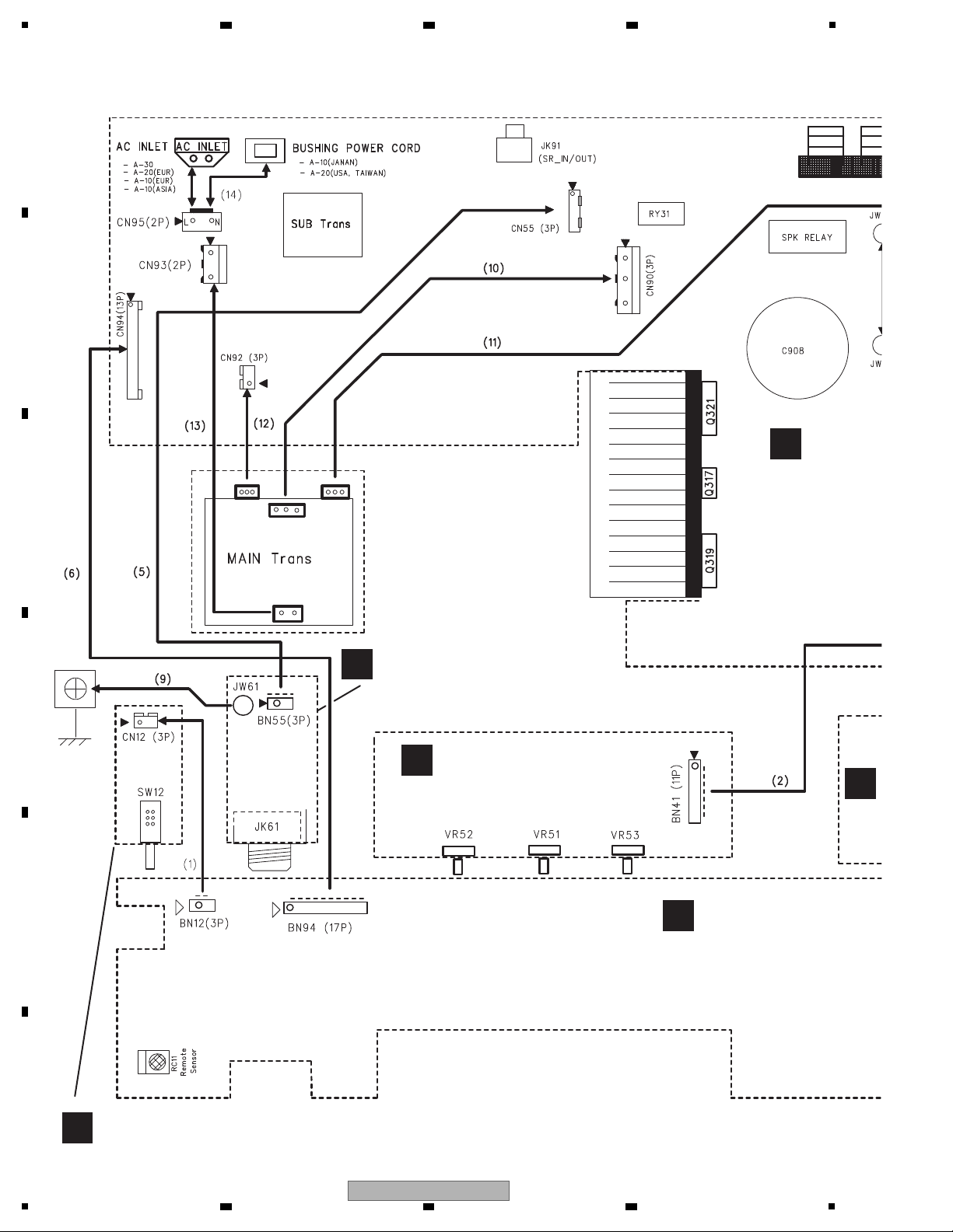
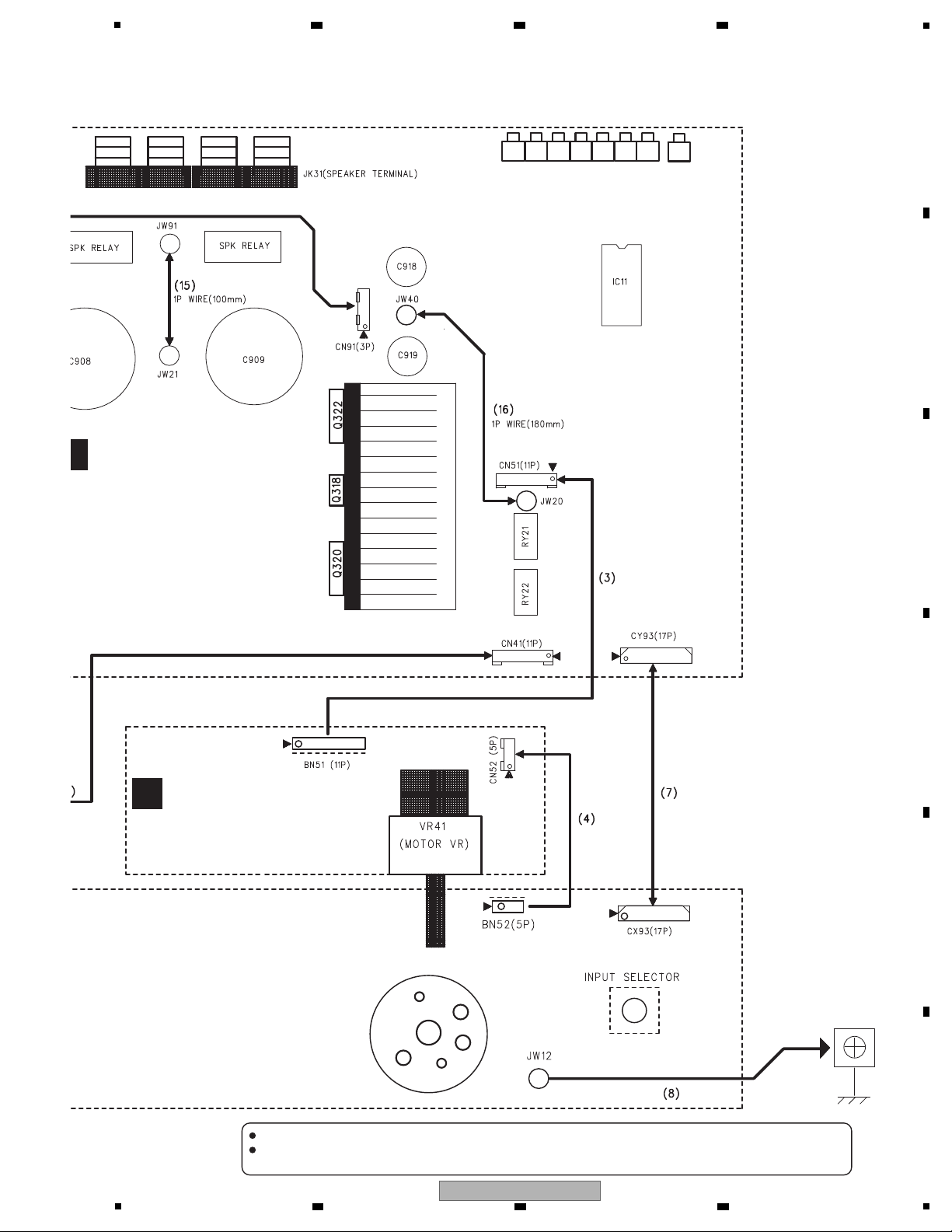
10. SCHEMATIC DIAGRAM
10.1 MAIN ASSY
A
B
C
D
E
F
40
1
2 3 4
A-30-K
Page 41

5
A
JK91
CN96
CN93
CN92
CN91
CN90
CN55
JK31
E
BN55
MAIN ASSY
(A-30-K/-S : AZW7487)
(A-20-K/-S : AZW7489)
(A-20 : AZW7490)
(A-10-K/-S : AZW7491)
A
Therefore, when replacing, be sure to use parts of identical designation.
When ordering service parts, be sure to refer to "EXPLODED VIEWS and PARTS LIST" or "PCB PARTS LIST".
The > mark found on some component parts indicates the importance of the safety factor of the part.
ACH7378
6 7 8
A
B
C
D
E
F
5
6 7 8
A-30-K
41
Page 42

1
XB
A
CN94
A
CY93
BN94
CX93
2 3 4
10.2 FRONT ASSY and SECOND POWER SW ASSY (A-30/A-20)
A
B
C
D
E
F
42
A-30-K
1
2 3 4
Page 43

5
FB
C
CN52
FRONT ASSY
(A-30-K/-S : AZW7482)
(A-20-K/-S : AZW7483)
(A-20 : AZW7484)
(A-10-K/-S : AZW7485)
B
SECOND POWER SW ASSY
(A-30-K/-S, A-20-K/-S, A-20 : AZW7478)
F
BN52
CN12
BN12
6 7 8
A
B
C
D
E
F
A-30-K
5
6 7 8
43
Page 44

1
C
MASTER VOLUME ASSY
(A-30-K/-S : AZW7476)
(A-20-K/-S, A-20, A-10-K/-S : AZW7481)
C
BN51
CN52
A
CN51
B
BN52
2 3 4
10.3 MASTER VOLUME ASSY, TONE ASSY and HEADPHONE ASSY
A
B
C
D
E
F
44
1
2 3 4
A-30-K
Page 45

ED
TONE ASSY
(AZW7477)
D
HEADPHONE ASSY
(AZW7479)
E
A
CN41
BN55
A
CN55
BN41
5
6 7 8
A
B
C
D
E
F
A-30-K
5
6 7 8
45
Page 46

1
A
BN94
CN94
B
AC IN
CN96
CN93
CN92 CN90 CN91
TRANSFORMER
BN55
CN55
E
SIDE A
MAIN ASSY
A
NOTE FOR PCB DIAGRAMS :
1. The parts mounted on this PCB include all
necessary parts for se veral destinations.
For further information for respective
destinations, be sure to check with the
schematic diagram.
CapacitorConnector
P.C. Bo ard Chip Part
SIDE A
SIDE B
2. Vie w point of PCB diagrams.
2 3 4
11. PCB CONNECTION DIAGRAM
11.1 MAIN ASSY
A
B
C
D
E
F
46
1
A-30-K
2 3 4
Page 47

5
A
BN51
CN51
C
BN41
CN41
D
CX93
CY93
B
SIDE A
6 7 8
A
B
C
D
E
F
A-30-K
5
6 7 8
47
Page 48

A
A
CN91
CN51
CN41CY93
SIDE B
MAIN ASSY
A
B
1
2 3 4
C
D
E
F
48
1
A-30-K
2 3 4
Page 49

5
A
CN94
CN93
CN92
CN90
CN55
CN96
SIDE B
6 7 8
A
B
C
D
E
F
A-30-K
5
6 7 8
49
Page 50

1
B
CN12
BN12
F
CN94
BN94
A
BN94
BN12
SIDE B
SIDE A
FRONT ASSY
B
FRONT ASSY
B
11.2 FRONT ASSY
A
2 3 4
B
C
D
E
F
50
A-30-K
1
2 3 4
Page 51

5
B
CN52
BN52
C
CY93
CX93
BN52 CX93
A
SIDE B
SIDE A
6 7 8
A
B
C
D
E
F
A-30-K
5
6 7 8
51
Page 52

1
C C
CN51
BN51
BN51
A
BN52
CN52
CN52
B
SIDE B
SIDE B
SIDE A
SIDE A
MASTER VOLUME ASSY
C
MASTER VOLUME ASSY
C
11.3 MASTER VOLUME ASSY
A
2 3 4
B
C
D
E
F
52
1
2 3 4
A-30-K
Page 53

5
D D
CN41
BN41
BN41
A
SIDE B SIDE B
SIDE A
SIDE A
TONE ASSY
D
TONE ASSY
D
11.4 TONE ASSY
6 7 8
A
B
C
D
E
F
A-30-K
5
6 7 8
53
Page 54

1
E F FE
CN55
BN55
A
BN12
CN12
BN55
CN12
B
SIDE B
SIDE B
SIDE A
SIDE A
HEADPHONE ASSY
E
SECOND POWER SW ASSY
F
HEADPHONE ASSY
E
SECOND POWER SW ASSY
F
2 3 4
11.5 HEADPHONE ASSY and SECOND POWER SW ASSY (A-30/A-20)
A
B
C
D
E
F
54
1
2 3 4
A-30-K
Page 55

5
5 6 2 1
1 R 0
R 5 0
5 6 1
4 7 3
NOTES: - Parts marked by “NSP” are generally unavailable because they are not in our Master Spare Parts List.
-
The > mark found on some component parts indicates the importance of the safety factor of the part.
Therefore, when replacing, be sure to use parts of identical designation.
-
When ordering resistors, first convert resistance values into code form as shown in the following examples.
Ex.1 When there are 2 effective digits (any digit apart from 0), such as 560 ohm and 47 k ohm (tolerance is shown by J = 5%,
and K = 10%).
560 Ω → 56 × 101 → 561
...................................................................
RD1/4PU J
47 kΩ → 47 × 10
3
→ 473
...................................................................
RD1/4PU J
0.5 Ω → R50
.................................................................................................
RN2H K
1 Ω → 1R0
.................................................................................................
RS1P K
Ex.2 When there are 3 effective digits (such as in high precision metal film resistors).
5.62 kΩ → 562 × 101 → 5621
.................................................................
RN1/4PC F
12. PCB PARTS LIST
6 7 8
A
[Wiring number reading substitute list]
SCHEMATIC
DIAGRAM, PCB
JK11 JA11 CJJ4N034Z MAIN
JK12 JA12 CJJ4P028Z MAIN
JK13 JA13 CJJ4P028Z MAIN
JK14 JA14 CJJ4P028Z MAIN
JK15 JA15 CJJ4N034Z MAIN
JK31 JA31 CJJ5Q006Z MAIN
JK91 JA91 HJJ1D002Z MAIN
RC11 IC1011 CRVKSM601TE5CA FRONT
BN12 J12 CWB1B00308047 FRONT
BN52 J52 CWB1B00515047 FRONT
BN94 J94 CWB1B01335047 FRONT
SW11 S11 CSR2A056Z FRONT
BN51 J51 CWB1C0112004W001 MASTER VOLUME
BN41 J41 CWB1B01120047 T ONE
BN55 J55 CWB4B00340047 HEADPHONE
JK61 JA61 CJJ2E020Z HEADPHONE
SW12 S12 CSH2B024Z SECOND POWER SW
Mark No. Description Part No.
LIST OF ASSEMBLIES
NSP 1..MAIN ASSY (A-30-K/-S) COP12421B
2..MAIN ASSY AZW7487
NSP 1..MAIN ASSY (A-20-K/-S) COP12421D
2..MAIN ASSY AZW7489
NSP 1..MAIN ASSY (A-20) COP12421E
2..MAIN ASSY AZW7490
NSP 1..MAIN ASSY (A-10-K/-S) COP12421F
2..MAIN ASSY AZW7491
NSP 1..FRONT ASSY (A-30-K/-S) COP12422B
2..FRONT ASSY AZW7482
2..MASTER VOLUME ASSY AZW7476
2..TONE ASSY AZW7477
2..HEADPHONE ASSY AZW7479
2..SECOND POWER SW ASSY AZW7478
Parts List Parts No. Name of Assembly
Mark No. Description Part No.
NSP 1..FRONT ASSY (A-20) COP12422G
2..FRONT ASSY AZW7484
2..MASTER VOLUME ASSY AZW7481
2..TONE ASSY AZW7477
2..HEADPHONE ASSY AZW7479
2..SECOND POWER SW ASSY AZW7478
NSP 1..FRONT ASSY (A-10-K/-S) COP12422D
2..FRONT ASSY AZW7485
2..MASTER VOLUME ASSY AZW7481
2..TONE ASSY AZW7477
2..HEADPHONE ASSY AZW7479
B
C
D
E
NSP 1..FRONT ASSY (A-20-K/-S) COP12422C
2..FRONT ASSY AZW7483
2..MASTER VOLUME ASSY AZW7481
2..TONE ASSY AZW7477
2..HEADPHONE ASSY AZW7479
2..SECOND POWER SW ASSY AZW7478
5
6 7 8
A-30-K
F
55
Page 56

1
CAUTIONS
The parts number of Q317, Q318 (BIAS Transistor), Q319, Q320,
Q321, Q322 (Power Transistor) and TH31, TH32 (Posistor) are
indicated in [9.2 EXTERIOR SECTION (A-30/A-20)] and
[9.3 EXTERIOR SECTION (A-10)] of [9. EXPLODED VIEWS
AND PARTS LIST]
2 3 4
A MAIN ASSY
AZW7487, AZW7489, AZW7490 and AZW7491 are constructed the same except for the following:
A
Symbol and
Mark
Description
JA15 CJJ4N034Z Not used Not used Not used
RY22 CSL4B022ZE Not used Not used Not used
RY32 CSL4B023ZE CSL4B024ZE CSL4B024ZE CSL4B024ZE
RY33 CSL4B023ZE CSL4B024ZE CSL4B024ZE CSL4B024ZE
T901 CLT5I010ZE CLT5I010ZE CLT5I010ZU CLT5I010ZE
C908 ACH7378 CCET50 VPLP822NCP CCET50VPLP822NCP CCET50VPLP822NCP
C909 ACH7378 CCET50 VPLP822NCP CCET50VPLP822NCP CCET50VPLP822NCP
AZW7487AZW7489
AZW7490 AZW7491
B FRONT ASSY
B
AZW7482, AZW7483, AZW7484 and AZW7485 are constructed the same except for the following:
Symbol and
Mark
Description
D109 CVDGY34MD22B51CMCACL CVDGY34SU05R41BJDABJ CVDGY34SU05R41BJDABJ CVDGY34SU05R41BJDABJ
D110 CVDGY34MD22B51CMCACL CVDGY34SU05R41BJDABJ CVDGY34SU05R41BJDABJ CVDGY34SU05R41BJDABJ
D111 CVDGY34MD22B51CMCACL CVDGY34SU05R41BJDABJ CVDGY34SU05R41BJDABJ CVDGY34SU05R41BJDABJ
D112 CVDGY34MD22B51CMCACL CVDGY34SU05R41BJDABJ CVDGY34SU05R41BJDABJ CVDGY34SU05R41BJDABJ
D114 CVDGY34MD22B51CMCACL CVDGY34SU05R41BJDABJ CVDGY34SU05R41BJDABJ CVDGY34SU05R41BJDABJ
D115 CVDGY34MD22B51CMCACL CVDGY34SU05R41BJDABJ CVDGY34SU05R41BJDABJ CVDGY34SU05R41BJDABJ
D116 CVDGY34MD22B51CMCACL CVDGY34SU05R41BJDABJ CVDGY34SU05R41BJDABJ CVDGY34SU05R41BJDABJ
D117 CVDGY34MD22B51CMCACL CVDGY34SU05R41BJDABJ CVDGY34SU05R41BJDABJ CVDGY34SU05R41BJDABJ
C
D118 CVDGY34MD22B51CMCACL CVDGY34SU05R41BJDABJ CVDGY34SU05R41BJDABJ CVDGY34SU05R41BJDABJ
D119 CVDGY34MD22B51CMCACL CVDGY34SU05R41BJDABJ CVDGY34SU05R41BJDABJ CVDGY34SU05R41BJDABJ
D120 CVDGY34MD22B51CMCACL Not used Not used Not used
S101 Not used Not used Not used CST1A023ZT
S106 CST1A023ZT Not used Not used Not used
AZW7482AZW7483AZW7484AZW7485
PCB PARTS LIST FOR A-30-K/-S UNLESS OTHERWISE NOTED
Mark No. Description Part No.
MAIN ASSY
A
D
SEMICONDUCTORS
IC 20 HVINJM2068MDTE1
IC 21 HVILC78212
IC 22,23,26 CVIAZ4580MTR-E1
IC 24 CVINJU7181RB1
IC 25 HVITC74HCT7007F
IC 91 CVINJU7223F33
IC 93,94 CVILM7815FTL
IC 95 CVIISP278R05FTL
Q 301-306,311,312 CVTKSC1845FTA
Q 307-310 CVTKSA992FTA
E
Q 313,314 HVTKTA1360Y
Q 315,316 HVTKTC3423Y
Q 323,324 HVTKTC3198YT
D 901 HVDGBJ806
D 902-905,908,909 CVD1N4003ST
D 906,907,918 CVDRB521S-30
D 912-917 CVD1N4003ST
MISCELLANEOUS
L 301,302 COIL , SPEAKER(0.5UH) CLEY0R5KAK
F
JA 11,15 JACK , IN/OUT CJJ4N034Z
JA 12-14 JACK , IN/OUT CJJ4P028Z
JA 31 TERMINAL , SPEAKER CJJ5Q006Z
JA 91 JACK , STEREO(2P 3.5PIE) HJJ1D002Z
56
1
2 3 4
A-30-K
Mark No. Description Part No.
VR 31,32 RES , SEMI FIXED (220 OHM) CVN12A221B03T
RY 21,22 RELAY , BC3-24H , DC24V , 2C2P CSL4B022ZE
RY 31 RELAY , BC3-24H , DC24V , 2C2P CSL4B022ZE
RY 32,33 RELAY , HL3-2A-24 , DC24V , 2C2P CSL4B023ZE
RY 91 RELAY,G5PA-1,DC6V,1C1P CSL1E002ZE
T 901 TRANS , SUB RCD-M37EUR CLT5I010ZE
RESISTORS
R 347-350 CRG1SANJ3R3RT
R 351-354 CRG1SANJ180RT
R 355,356,369,370 CRF5EKR22H
R 371,372,375,376 CRG1ANJ100H
R 933,934 CRQ1AJR47H
CAPACITORS
C 278 CCEA1EH102ECP
C 918,919 CCEA1EH222ECP
C 927,933,937,950 CCEA1CH102ECP
C 938 CCEA0JH102T
C 947,948 KCKDKS472ME
Page 57

5
6 7 8
Mark No. Description Part No.
FRONT ASSY
B
SEMICONDUCTORS
IC 11 CVIANAM1656A
IC 12 CVIML61C282PR
IC 1011 CRVKSM601TE5CA
D105
D 106 CVDBLBUF4V5K1AV
D 107,109-112
D 114-120
MISCELLANEOUS
J 12 ROCKING TYPE WIRE ASSY CWB1B00308047
(3P, 80MM, 2.0MM)
J 52 ROCKING TYPE WIRE ASSY CWB1B00515047
(5P, 150MM, 2.0MM)
J 94 ROCKING TYPE WIRE ASSY CWB1B01335047
(13P, 350MM, 2.0MM)
S 11 VR, ENCODER CSR2A056Z
S 102-106 SW , TACT CST1A023ZT
MASTER VOLUME ASSY
C
SEMICONDUCTORS
IC 41 CVIAZ4580MTR-E1
IC 42 CVIBU4052BCF
CVDGY34MU22Y16BJTAA4
CVDGY34MD22B51CMCACL
CVDGY34MD22B51CMCACL
Mark No. Description Part No.
HEADPHONE ASSY
E
MISCELLANEOUS
J 55 ROCKING TYPE WIRE ASSY CWB4B00340047
(3P, 400MM, 2.0MM)
JA 61 JACK, PHONES(6.35MM,GOLD) CJJ2E020Z
RESISTORS
R 601,602 CRD25TJ470T
SECOND POWER SW ASSY(A-30/A-20)
F
MISCELLANEOUS
S 12 SW, PUSH (FOR DC , 2C2P) CSH2B024Z
A
B
C
MISCELLANEOUS
J 51 ROCKING TYPE SHIELD WIRE ASSY CWB1C0112004W001
(11P, 200MM, 2.0MM)
VR 41 VOLUME , MOTOR CVV9Y13B503Z
RESISTORS
R 403 CRD25TJ100T
CAPACITORS
C 440 CCEA0JH102TC
TONE ASSY
D
SEMICONDUCTORS
IC 51,52 CVIAZ4580MTR-E1
MISCELLANEOUS
J 41 ROCKING TYPE WIRE ASSY CWB1B01120047001
(11P, 200MM, 2.0MM)
VR 51,52 RES, VARIABLE(ANGLE) CVV3W01B103Z
VR 53 RES, VARIABLE(ANGLE) CVV3W02M203Z
RESISTORS
R 503,514 CRD25TJ100T
D
E
F
A-30-K
5
6 7 8
57
 Loading...