

Page 1

DVD-Video Recorder DVD+RW Basic Engine
VAE8015
VAE8020
Contents Page
1 Technical Specifications 2
2 Safety Instructions, Warnings and Notes 3
3 Directions for Use (No DFU necessary) 4
4 Mechanical Instructions 5
5 Service Modes, Error Codes and Fault Finding 7
6 Block Diagram and Testpoint Overviews
Block Diagram 17
Testpoint Overview Servo Board 43015 18
Testpoint Overview Servo Board 43353 19
7 Electrical Diagrams and Print-Layouts Diagram PWB
Servo Board 43015: Processor (Diagram 1) 20 25-26
Servo Board 43015: MACE 3 (Diagram 2) 21 25-26
Servo Board 43015: Driver (Diagram 3) 22 25-26
Servo Board 43015: Dec./Encoder (Diagram 4) 23 25-26
Servo Board 43015: Power (Diagram 5) 24 25-26
Servo Board 43353: Processor (Diagram 1) 27 32-33
Servo Board 43353: MACE 3 (Diagram 2) 28 32-33
Servo Board 43353: Driver (Diagram 3) 29 32-33
Servo Board 43353: Dec./Encoder (Diagram 4) 30 32-33
Servo Board 43353: Power (Diagram 5) 31 32-33
8 Alignments (No alignments necessary)35
9 Circuit Descriptions 35
List of Abbreviations 40
IC Data 41
10 Spare Parts List 42
©
Copyright 2002 Philips Consumer Electronics B.V. Eindhoven, The Netherlands.
All rights reserved. No part of this publication may be reproduced, stored in a
retrieval system or transmitted, in any form or by any means, electronic,
mechanical, photocopying, or otherwise without the prior permission of Philips.
Published by MW 0272 Service PaCE Printed in the Netherlands Subject to modification EN 3122 785 12471
Page 2

EN 2 VAE8015 / 80201.
Technical Specifications
1. Technical Specifications
VAE8010 functionality:
• Loading of 8 cm and 12 cm discs by a motorized tray
• Disc type recognition and in case of a DVD+RW disc laser
power calibration
• Servo control for disc rotation, sledge movements, tilt,
focus and actuator position
• EFM+ encoding / decoding for DVD, and EFM decoding for
CD
• Writes and read DVD+RW discs and reads DVD, CD and
CD-R/RW discs
• Linking control, header insertion and sector number
updating at record
• Interfacing to the MPEG back-end (S2B) for control and
(I2S and V4) for data
• The back-end has to provide MPEG data processing, data
buffering, construction
• of logical format for Lead-in, Data area and Lead-out part
of the DVD+RW dis
Page 3
Safety Instructions, Warnings and Notes
2. Safety Instructions, Warnings and Notes
EN 3VAE8015 / 8020 2.
2.1 Safety Instructions
2.1.1 General Safety
Safety regulations require that during a repair:
• Connect the unit to the mains via an isolation transformer.
• Replace safety components, indicated by the symbol ,
only by components identical to the original ones. Any
other component substitution (other than original type) may
increase risk of fire or electrical shock hazard.
Safety regulations require that after a repair, you must return
the unit in its original condition. Pay, in particular, attention to
the following points:
• Route the wires/cables correctly, and fix them with the
mounted cable clamps.
• Check the insulation of the mains lead for external
damage.
• Check the electrical DC resistance between the mains plug
and the secondary side:
1. Unplug the mains cord, and connect a wire between
the two pins of the mains plug.
2. Set the mains switch to the 'on' position (keep the
mains cord unplugged!).
3. Measure the resistance value between the mains plug
and the front panel, controls, and chassis bottom.
4. Repair or correct unit when the resistance
measurement is less than 1 MΩ.
5. Verify this, before you return the unit to the customer/
user (ref. UL-standard no. 1492).
6. Switch the unit ‘off’, and remove the wire between the
two pins of the mains plug.
2.1.2 Laser Safety
This unit employs a laser. Only qualified service personnel may
remove the cover, or attempt to service this device (due to
possible eye injury).
2.2 Warnings
2.2.1 General
• All ICs and many other semiconductors are susceptible to
electrostatic discharges (ESD, symbol ). Careless
handling during repair can reduce life drastically. Make
sure that, during repair, you are at the same potential as
the mass of the set by a wristband with resistance. Keep
components and tools at this same potential. Available
ESD protection equipment:
– Complete kit ESD3 (small tablemat, wristband,
connection box, extension cable and earth cable) 4822
310 10671.
– Wristband tester 4822 344 13999.
• Be careful during measurements in the live voltage section.
The primary side of the power supply (pos. 1005), including
the heatsink, carries live mains voltage when you connect
the player to the mains (even when the player is 'off'!). It is
possible to touch copper tracks and/or components in this
unshielded primary area, when you service the player.
Service personnel must take precautions to prevent
touching this area or components in this area. A 'lightning
stroke' and a stripe-marked printing on the printed wiring
board, indicate the primary side of the power supply.
• Never replace modules, or components, while the unit is
‘on’.
2.2.2 Laser
• The use of optical instruments with this product, will
increase eye hazard.
• Only qualified service personnel may remove the cover or
attempt to service this device, due to possible eye injury.
• Repair handling should take place as much as possible
with a disc loaded inside the player.
• Text below is placed inside the unit, on the laser cover
shield:
Laser Device Unit
Type : Semiconductor laser
GaAlAs
Wavelength : 650 nm (DVD)
: 780 nm (VCD/CD)
Output Power : 20 mW (DVD+RW
writing)
: 0.8 mW (DVD
reading)
: 0.3 mW (VCD/CD
reading)
Beam divergence : 60 degree
Figure 2-1 Class 1 Laser Product
Note: Use of controls or adjustments or performance of
procedure other than those specified herein, may result in
hazardous radiation exposure. Avoid direct exposure to beam.
CAUTION VISIBLE AND INVISIBLE LASER RADIATION WHEN OPEN AVOID EXPOSURE TO BEAM
ADVARSEL SYNLIG OG USYNLIG LASERSTRÅLING VED ÅBNING UNDGÅ UDSÆTTELSE FOR STRÅLING
ADVARSEL SYNLIG OG USYNLIG LASERSTRÅLING NÅR DEKSEL ÅPNES UNNGÅ EKSPONERING FOR STRÅLEN
VARNING SYNLIG OCH OSYNLIG LASERSTRÅLNING NÄR DENNA DEL ÄR ÖPPNAD BETRAKTA EJ STRÅLEN
VARO! AVATTAESSA OLET ALTTIINA NÄKYVÄLLE JA NÄKYMÄTTÖMÄLLE LASER SÄTEILYLLE. ÄLÄ KATSO SÄTEESEEN
VORSICHT SICHTBARE UND UNSICHTBARE LASERSTRAHLUNG WENN ABDECKUNG GEÖFFNET NICHT DEM STRAHL AUSSETSEN
DANGER VISIBLE AND INVISIBLE LASER RADIATION WHEN OPEN AVOID DIRECT EXPOSURE TO BEAM
ATTENTION RAYONNEMENT LASER VISIBLE ET INVISIBLE EN CAS D'OUVERTURE EXPOSITION DANGEREUSE AU FAISCEAU
!
Figure 2-2 Warning text
Page 4

EN 4 VAE8015 / 80203.
3. Directions For Use
Not applicable
Directions For Use
Page 5
4. Mechanical Instructions
Mechanical Instructions
EN 5VAE8015 / 8020 4.
Index of this chapter:
1. General
2. Disassembly
3. Re-assembly
Note: Figures below can deviate slightly from the actual
situation, due to the different set executions.
4.1 General
• Follow the disassemble instructions in described order.
• Do not place the unit with its PWB on a hard surface (e.g.
table), as it could damage the components on it. Always
place something soft (a towel or foam cushion) under it.
• Never touch the lens of the laser.
• Take sufficient ESD measures during (dis)assembly.
4.2 Disassembly
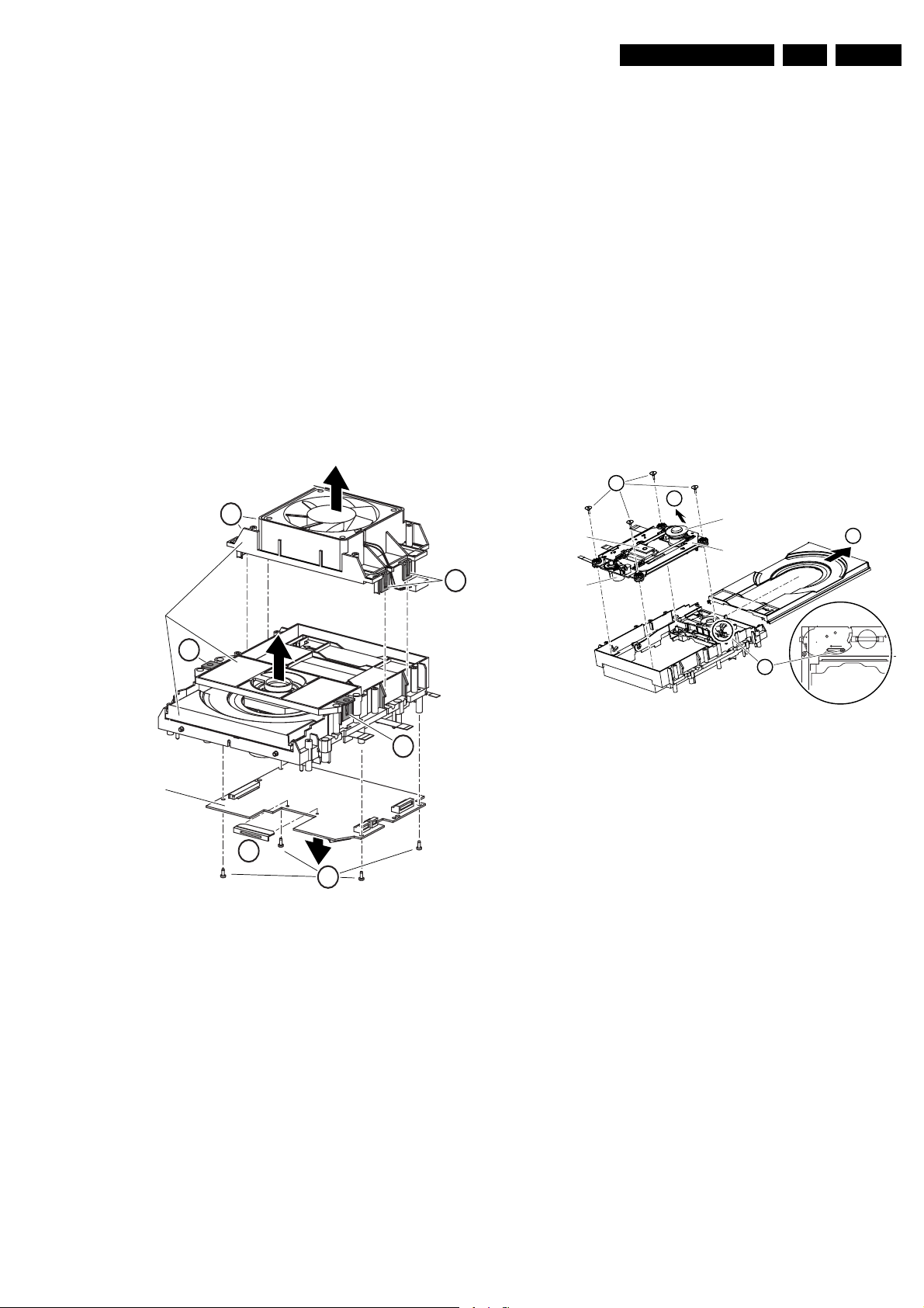
1
Loader
4.2.2 PWB
1. Flip the module180 degrees, so you can access the PWB.
2. Disconnect the four flex foils from the PWB connectors
(1100, 1300, 1302, and 1303) at the component side. For
the flex foil on connector 1100, you first must remove the
cable clamp [3]. The easiest way to do this is to push down
the two fixation pins of the clamp (via the holes in the PWB)
by means of a pencil or small screwdriver.
3. Disconnect the remaining cables (tray- and fan-motor
cable) at the solder side of the PWB
4. Remove the four screws (Torx 8) that hold the PWB [4].
5. Now you can remove the board.
4.2.3 DVD-M
Caution: Never try to align the DVD-Module! ! ! Only the factory
can do this properly. Service engineers are only allowed to
exchange the sledge motor assy.
3
4
Disc
OPU
1
monitor
Tilt
motor
DVD-M
2
2
PWB
3
4
CL 26532126_010.eps
Figure 4-1 Basic Engine disassembly (part 1)
You can divide the Basic Engine into the following parts:
1. Loader (fan, clamp, and tray assy).
2. PWB (or 'mono board').
3. DVD-Module (OPU, turntable motor, and sledge-motor
assy).
4.2.1 Loader
2
191102
1
CL 26532126_011.eps
191102
Figure 4-2 Basic Engine disassembly (part 2)
1. Slide the 'tray pin' in the direction of the arrow [1], in order
to release the disc tray.
2. Flip the module180 degrees and pull out the tray [2]. Now
you can access the DVD-Module.
3. Remove the four screws [3] with a Torx 6 screwdriver, and
lift the DVD-M upwards [4] at the side of the disc-motor. It
hinges in the bracket at the side of the tilt-motor.
1. Disconnect the 2-wire fan cable from the PWB.
2. Remove the fan assy, by releasing the four side clamps [1]
while moving it upwards.
3. Remove the clamp assy, by releasing the two side clamps
[2] while moving it upwards.
Page 6
EN 6 VAE8015 / 80204.
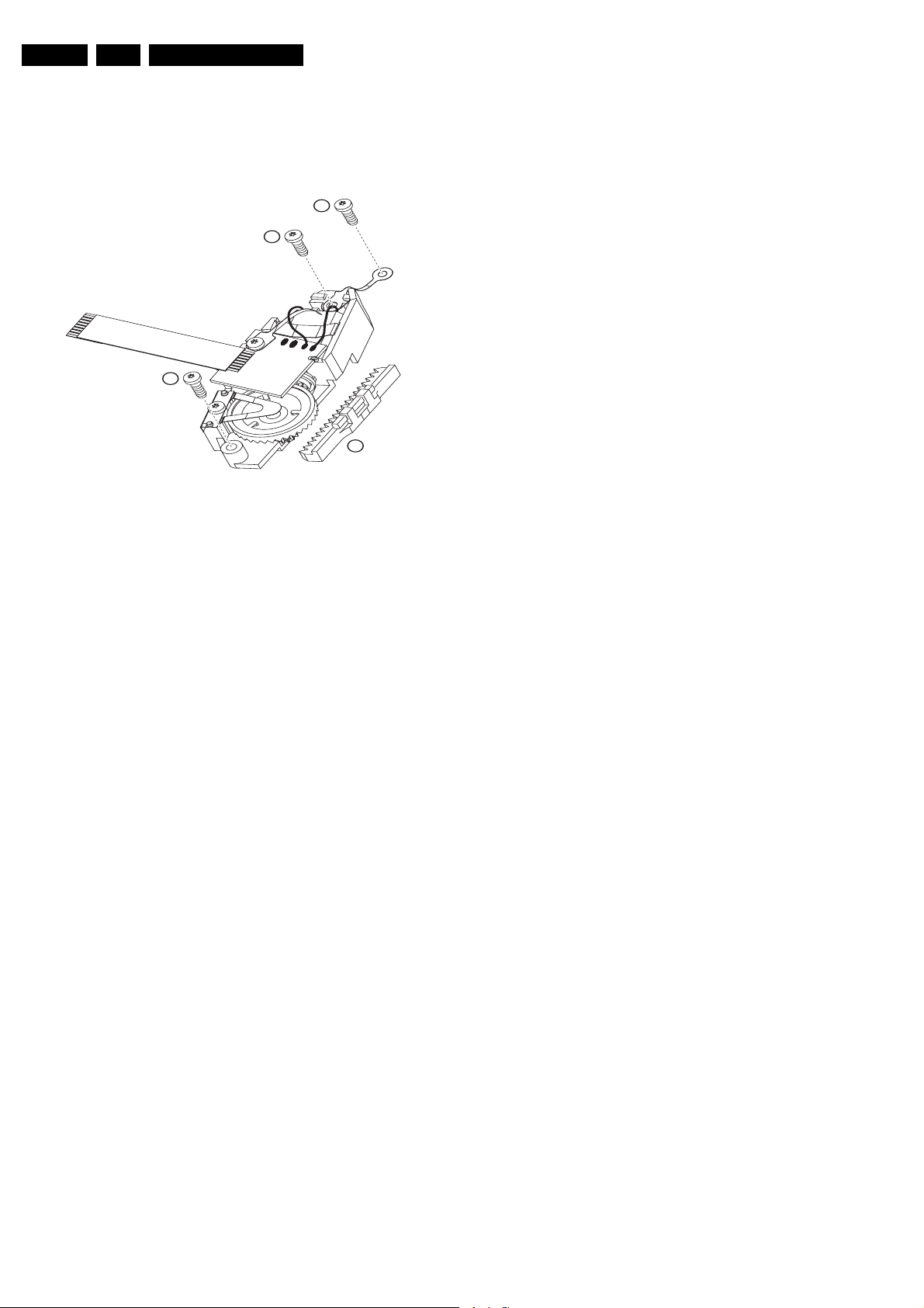
4.2.4 Sledge-motor Assy
Caution: Never try to align the DVD-Module! ! ! Only the factory
can do this properly. Service engineers are only allowed to
exchange the sledge motor assy.
1
1
Mechanical Instructions
1
2
CL 26532126_014.eps
191102
Figure 4-3 Sledge-motor assy
1. Place the DVD-Module, with the laser facing downwards,
on a soft surface.
2. Remove the three screws [1] that hold the sledge-motor
assy, and lift the assy upwards. You can replace it now.
3. If necessary, it is now also possible to replace the sledgerack [2] that is hinged in the sledge assy.
4.3 Re-assembly
To re-assemble the module, do all processes in reverse order.
Be sure to:
• Sledge-motor assy: Mesh the teeth of the sledge motor
and sledge rack properly, during mounting of the sledgemotor assy.
• DVD-M: Point the laser up (towards the tray), when you
mount the DVD-M in the bracket.
• Complete module: Place all wires/cables in their original
positions
Page 7
Service Modes, Error Codes and Fault Finding
5. Service Modes, Error Codes and Fault Finding
EN 7VAE8015 / 8020 5.
Index of this chapter:
1. General
2. Start-up Measurements
3. Diagnostic Software
4. Nuclei Error Codes
5. Fault Finding
5.1 General
• Impedance of measuring-equipment should be > 1 MOhm.
• For testing the Basic Engine, connect it to a DVD-recorder
of the DVDR1000, 900, or 800 series.
• Most tests are done by software commands. Together with
the software command you will find a Ref.# nbr. This is the
number of the diagnostic nucleus used for this test. You
can find information that is more detailed in the chapter
'Diagnostic Nuclei'.
• Levels: Most measurements are digital measurements.
The signal levels specification in this document are defined
as follows:
– low < 0.3V
– high > 3.0V
– LOW < 0.4V
– HIGH > 4.5V
5.2 Start-up Measurements
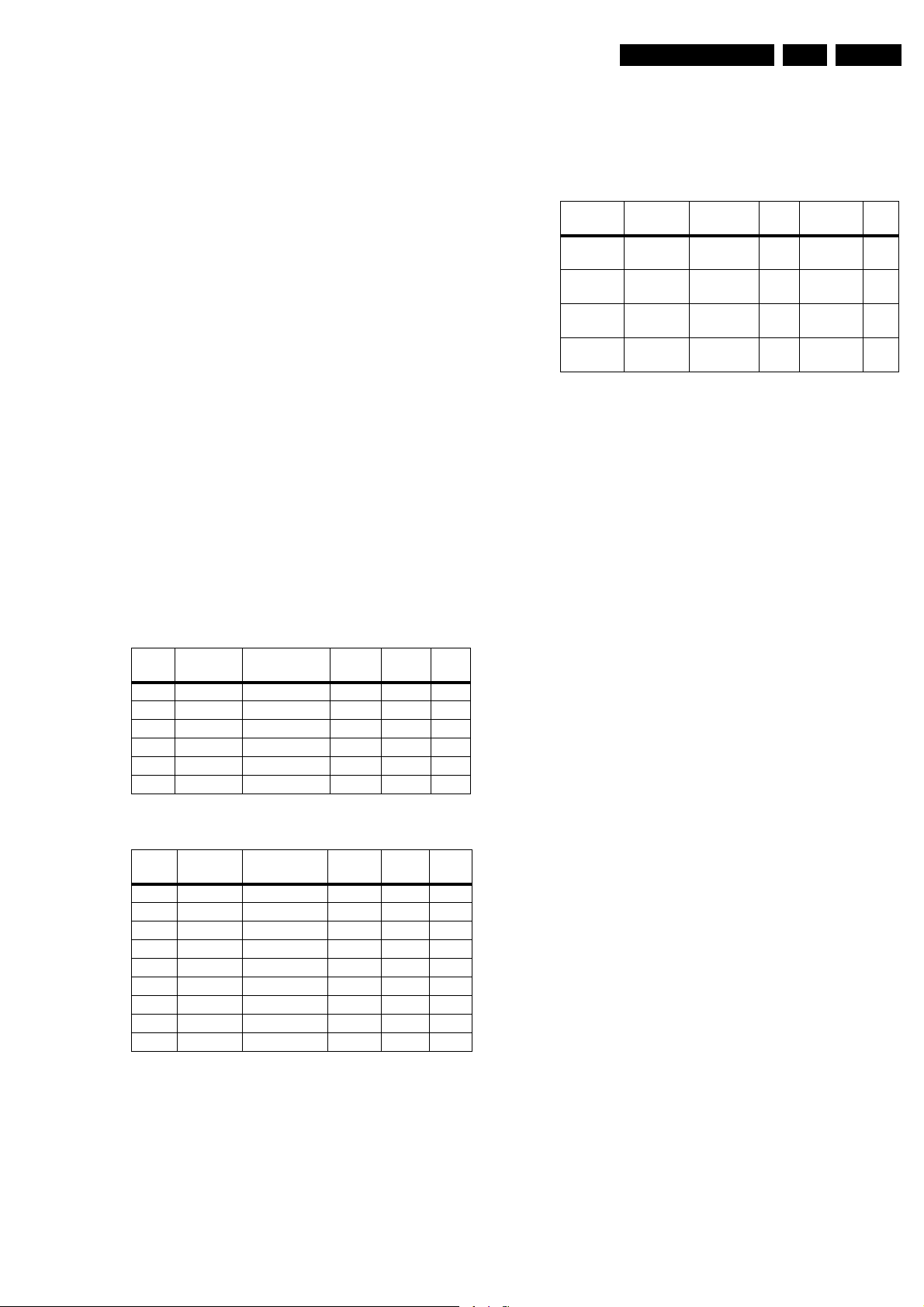
5.2.1 Power Supply Check
Table 5-1 Table of supply input voltages.
Signal Test point Description Specifi-
cations
+3V3 I007 Input of supply +3.3 1% V
+5 I008 Input of supply +5 1% V
+4V6 I010 Input of supply +4.6 1% V
-5 I011 Input of supply -5 1% V
+12 I012 Input of supply +2 1% V
GND I01 5, I016 Input of supply
Table 5-2 Table of derived supply voltages.
Signal Test point Description Specifi-
cations
D3V3 I006 Digital 3V3 +3.3 2% V
A3V3 I007 Analogue 3V3 +3.3 2% V
+5V I008 Analogue 5V +5 2% V
D5V I009 Digital 5V +5 2% V
+3V3E F001 OPU 3V3 +3.3 2% V
-5 I011 Neg. voltage -5 2% V
+12 I012 12V +12 2% V
Vbias I014 Bias voltage -1.7 2% V
GND I017, I018 Input of supply 0 0 % V
The module operates in power 'off' and power 'on' only. There
is no standby mode at module level. In power 'off', the module
does not respond to any communication or signal.
Before starting the measurement, connect the power supply to
the mono board via connector 1000, and the PC interface cable
to the Service Interface connector of the 'test recorder'.
Tolerance
Tolerance
Unit
Unit
5.2.2 Oscillator Check
Table 5-3 Table of clock signals.
Signal Test point Descrip-
tion
OSCOUT I219 Ref. Clock
MACE
CROUT I443 Ref. Clock
PSEN I223 OEN Flas h
RA/FO/SL I326/I334/
I343
On the mono board, there are two external oscillators
(OSCOUT and CROUT), which are the reference for all clock
signals derived in several ICs.
To check whether the program (in the MACE microprocessor)
is running after power 'on', you can monitor the PSEN (OEn of
Flash ROM) on I223 (see test point overview in chapter 6).
You can measure the Servo clocks at I326 (RAdial), I334
(FOcus), and I343 (SLedge).
HDR65
ROM
Servo clock 2.120 +/- 20 kHz MHz
Spec. Toler-
8.483 +/- 70 kHz MHz
8.501 +/- 70 kHz MHz
5.324 +/- 70 kHz MHz
5.3 Diagnostic Software
Due to the complexity of a DVD recorder, the time to find a
defect in the recorder can become long. To reduce this time,
the recorder has been equipped with Diagnostic and Service
software (DS). The DS offers functionality to diagnose the
DVDR hardware and tests the following:
• Interconnections between components.
• Accessibility of components.
• Functionality of the audio and video paths.
This is also valid for the Basic Engine.
One can access this functionality via several interfaces:
1. End user/Dealer script interface.
2. Player script interface.
3. Menu and command interface.
This part describes all interfaces from the outside world to the
diagnostic software, how to use these interfaces, and how to
access them.
First some definitions:
• Diagnostic Nucleus. Part of the Diagnostic Software.
Each nucleus contains an atomic and software
independent diagnostic test, testing a functional part of the
DVD player hardware on component level.
• Script. Part of the Diagnostic Software. Each script
contains a sequence of Diagnostic Nuclei to be executed.
• Service PC. PC used by a service or repair person to
communicate with the Diagnostic Software in the DVD
player.
5.3.1 End User/Dealer Script Interface
The End user/Dealer script interface gives a diagnosis on a
stand-alone DVD recorder; no other equipment is needed.
During this mode, a number of hardware tests (nuclei) are
automatically executed to check if the recorder is faulty. The
diagnosis is simply a 'fail' or 'pass' message. If the message
'FAIL' appears on the display, there is apparently a failure in the
recorder. If the message 'PASS' appears, the nuclei in this
mode have been executed successfully. There can be still a
failure in the recorder because the nuclei in this mode do not
cover the complete functionality of the recorder.
Unit
ance
Page 8
EN 8 VAE8015 / 80205.
Service Modes, Error Codes and Fault Finding
Note: As this mode is meant for a complete DVD Recorder,
and does not add much for testing the Basic Engine, reference
is made to the appropriate DVD Recorder Service Manual for a
detailed description:
• DVDR1000: 3122 785 11600
• DVDR990: 3122 785 12430
• DVDR98x: 3122 785 11970
• DVDR8xx: 3122 785 12200
5.3.2 Player Script Interface
The Player script will give the opportunity to perform a test that
will determine which of the DVD recorder's modules are faulty,
to read the error log and to perform an endurance loop test. To
successfully perform the tests, connect the DVD recorder to a
TV set. To be able to check results of certain nuclei, the player
script expects some interaction of the user (i.e. to approve a
test picture or a test sound). Some nuclei (e.g. nuclei that test
functionality of the DVDR module) require that a DVD+RW disc
is inserted. Only tests within the scope of the diagnostic
software will be executed hence only faults within this scope
can be detected.
See note above (paragraph 5.3.1).
5.3.3 Menu and Command Interface
Each nucleus contains an atomic and independent diagnostic
test, testing a functional part of the DVD player hardware on
component level. Each Nucleus returns a result message to its
caller. Some tests (e.g. generating a colour bar) can only return
an "OK" result. Internal communication will be done via a
uniform interface between the diagnostic Engine, Scripts, and
the Diagnostic Nuclei.
The Diagnostic Engine can only operate if a certain (minimal)
set of hardware is functioning properly. To test this set of
hardware, a set of basic diagnostic nuclei is embedded in the
DVD player. Each basic diagnostic nucleus will only test that
part of the hardware which is required for execution of the
diagnostic Engine, e.g. a RAM test will only test that part of
RAM that is used by the diagnostic engine. After the Diagnostic
Engine is operational, it is possible to do a full RAM diagnostic.
All basic diagnostic nuclei start with prefix 'Basic'. In the
overview, each Diagnostic Nucleus consists of a reference
number, a reference name, and remarks. Reference number
and name are coupled and one of them is enough for unique
identification.
Nuclei Numeration
Each nucleus has a unique number of four digits. This number
is the input of the command mode.
[ XX YY ]
Group number Group name
4 NVRAM
5 Front Panel
6 Basic Engine
7 Analogue board (DVDR only)
8 DVIO (DVDR only)
9 Loop nuclei (DVDR only)
10 Library sub nuclei (I2C nuclei)
11 User interface
12 Furore (SACD only)
13 DAC (SACD only)
14 Miscellaneous
For testing the Basic Engine, group number 6 is defined
Error handling
Each nucleus returns an error code. This code contains six
numerals, which means:
[ XX YY ZZ ]
Error code
Nucleus number
Nucleus group number
Figure 5-2 Error code
The nucleus group numbers and nucleus numbers are the
same as above.
Hardware required
• Service PC.
• One free COM port on the Service PC.
• Special cable to connect DVD recorder to Service PC.
The service PC must have a terminal emulation program (e.g.
OS2 Warp Terminal, ProComm, or HyperTerminal) installed
and must have a free COM port (e.g. COM1).
Activate the terminal emulation program and check that the
port settings for the free COM port are:
• 19200 bps,
• 8 data bits,
• No parity,
• 1 stop bit,
• No flow control.
Connect the free COM port via a special cable to the RS232
port of the DVD recorder. This special cable will also connect
the test pin, which is available on the connector, to ground (i.e.
activate test pin). Code number of PC interface cable: 3122
785 90017.
CL 06532152_013.eps
051200
Nucleus number
Nucleus group number
Figure 5-1 Nucleus code
The following groups are defined:
Table 5-4 Nucleus groups
Group number Group name
0 Basic / Scripts
1 Host decoder
2 Audio / Video encoder (DVDR only)
3 VSM (DVDR only)
CL 06532152_012.eps
051200
Command Mode Interface
Activation
Connect the recorder to the mains. The following text will
appear on the screen of the terminal (program):
DVD Video Recorder Diagnostic Software version 48
Basic SDRAM Data bus test passed
Basic SDRAM Address bus test passed
Basic SDRAM Device test passed
(M) enu, (C) ommand or (S) 2B-interface? [M] : @ C
DD:>
Figure 5-3 Opening screen for Command Mode
CL 16532095_073.eps
150801
Page 9
Service Modes, Error Codes and Fault Finding
EN 9VAE8015 / 8020 5.
The first line indicates that the Diagnostic software has been
activated and contains the version number. The next lines are
the successful result of the SDRAM interconnection test and
the basic SDRAM test. The last line allows the user to choose
between the three possible interface forms.
If pressing 'C' has made a choice for Command Interface, the
prompt ("DD>") will appear. The diagnostic software is now
ready to receive commands. The commands that can be given
are the numbers of the nuclei.
Command Overview
We provide an overview of the nuclei and their numbers. This
overview is preliminary and subject to modifications.
Table 5-5 Nuclei overview
Ref. # Function name Description
600 DS_BE_S2B_Pass It switches the RS232 port
and the S2B port in passthrough mode. This means
that the player hangs. The
only way to exit this nucleus
is via a power off of the player
601 DS_BE_S2B_Engine It checks the S2B interface
with the Basic Engine by
sending an 'echo' command
602 DS_BE_Version It returns the version number
of the Basic Engine
603 DS_BE_Reset It resets the Basic Engine
604 DS_BE_FocusOn It puts the laser of the basic
engine into focus (focus
loop)
605 DS_BE_FocusOff It switches the focus loop off
606 DS_BE_DiscMotorOn It switches the disk motor (=
spindle motor) on
607 DS_BE_DiscMotorOff It switches the disk motor (=
spindle motor) off
608 DS_BE_RadialOn It closes the radial loop
609 DS_BE_RadialOff It opens the radial loop
615 DS_BE_TrayIn It closes the disc tray
616 DS_BE_TrayOut It opens the disc tray
617 DS_BE_WriteRead It writes data to the BE which
is stored on a DVD disc and
read it back from the DVD
disc. This is only done when
the result of the self-test con-
tains no errors.
618 DS_BE_WriteReadE
ndlessLoop
It writes data to the BE which
is stored on a DVD disc and
read it back from the DVD
disc, while repeating in an
endless loop. This is only
done when the result of the
self-test contains no errors.
Errors are stored in NVRAM.
625 DS_BE_SledgeMotor
Slow
It moves the sledge full
stroke several times slow
enough to allow visual in-
spection of unhampered
movement
626 DS_BE_Tilt It tests the tilt mechanism
control loop, or allow its prop-
er functioning to be meas-
ured
627 DS_BE_ReadEepromIt reads one data byte from
the EEPROM
629 DS_BE_OptimiseJitterIt performs jitter optimisation
Ref. # Function name Description
630 DS_BE_RadialATLS
Calibration
631 DS_BE_GetStatistics
Info
It allows the radial loop to be
calibrated.
It retrieves the statistical information from the Basic Engine
632 DS_BE_ResetStatisti
csInfo
It erases the statistical information
633 DS_BE_ReadErrorlogIt retrieves the error log from
the Basic Engine
634 DS_BE_ResetErrorlogIt erases the fatal error log
and the cumulative error log
638 DS_BE_GetSelfTest
Result
It retrieves the result of the
Self Test of the Basic engine,
which is executed during
power-on.
639 DS_BE_RadialInit It allows the radial initialisa-
tion
640 DS_BE_GetOPUInfo It retrieves the OPU number
from the EEPROM of the Basic engine.
641 DS_BE_WriteReadPl
usR
It writes data to the BE which
is stored on a DVD disc and
read it back from the DVD
disc. This is only done when
the result of the self-test contains no errors.
642 DS_BE_WriteReadPl
usREndlessLoop
It writes data to the BE which
is stored on a DVD disc and
read it back from the DVD
disc, while repeating in an
endless loop. This is only
done when the result of the
self-test contains no errors.
Errors are stored in NVRAM.
Menu Mode Interface
Activation
Connect the recorder to the mains. The following text will
appear on the screen of the terminal (program):
DVD Video Recorer Diagnostic Software version 48
Basic SDRAM Data bus test passed
Basic SDRAM Address bus test passed
Basic SDRAM Device test passed
(M) enu, (C) ommand or (S) 2B-interface? [M] : @ M
Main Menu
1. Digital Board ->
2. Analogue Board ->
3. Front Panel ->
4. Basic Engine ->
5. DVIO ->
6. Progressive Scan Board ->
7. Loop tests ->
8. Log ->
9. Scripts ->
Select>
CL 16532095_074.eps
150801
Figure 5-4 Opening screen for Menu Mode
The first line indicates that the Diagnostic software has been
activated and contains the version number. The next lines are
the successful result of the SDRAM interconnection test and
the basic SDRAM test. The last line allows the user to choose
between the three possible interface forms.
If pressing 'M' has made a choice for Menu Interface, the Main
Menu will appear.
Page 10
EN 10 VAE8015 / 80205.
Service Modes, Error Codes and Fault Finding
Menu Structure
1. Digital Board
2. Analogue Board
3. Front Panel
4. Basic Engine
1. Reset
2. S2B Pass-through
3. S2B Echo
4. Focus On
5. Focus Off
6. Version
7. Self Test
8. Get Self Test Result
9. Basic Engine Test
10. Laser Test
11. Focus Test
12. Tilt Test
13. Optimise Jitter
14. Statistics Info
15. Log
1. Read Error Log
2. Reset Error LogSpindle Motor
16. Spindle Motor
1. Spindle Motor On
2. Spindle Motor Off
3. Spindle Motor Test
17. Radial
1. Radial On
2. Radial Off
3. Radial Initialisation
4. Radial ATLS Calibration
18. Sledge
1. Sledge test
2. Sledge test slow
19. Tray
1. Tray In
2. Tray Out
5. DVIO
6. Progressive Scan Board
7. Loop Tests
8. Log
9. Scripts
5.4 Nuclei Error Codes
In the following table the error codes will be described.
Table 5-6 Nuclei error codes overview
Error # Description
60000 The player hangs, the RS232 port and the S2B port
were successfully switched in pass-through mode.
The only way to exit is to power 'off' the player
60100 The S2B interface with the Basic Engine was suc-
cessfully checked
60101 The Basic Engine returned an error number
60102 Parity error from Basic Engine to Serial
60103 Communication time-out error
60104 Unexpected response from Basic Engine
60105 The Echo loop could not be closed
60106 A wrong echo pattern was received
Error # Description
60300 The Basic Engine was successfully reset
60301 Basic-Engine time-out error
60400 The focus on test was successfully completed
60401 The Basic Engine returned an error number
60402 Parity error from Basic Engine to Serial
60403 Communication time-out error
60404 Unexpected response from Basic Engine
60405 Focus loop could not be closed
60500 The focus off test was successfully completed
60501 The Basic Engine returned an error number
60502 Parity error from Basic Engine to Serial
60503 Communication time-out error
60504 Unexpected response from Basic Engine
60600 The disk motor was successfully switched on
60601 The Basic Engine returned an error number
60602 Parity error from Basic Engine to Serial
60603 Communication time-out error
60604 Unexpected response from Basic Engine
60700 The disk motor was successfully switched off
60701 The Basic Engine returned an error number
60702 Parity error from Basic Engine to Serial
60703 Communication time-out error
60704 Unexpected response from Basic Engine
60800 The Radial loop was successfully closed
60801 The Basic Engine returned an error number
60802 Parity error from Basic Engine to Serial
60803 Communication time-out error
60804 Unexpected response from Basic Engine
60805 The Radial loop could not be closed
60900 The Radial loop was successfully opened
60901 The Basic Engine returned an error number
60902 Parity error from Basic Engine to Serial
60903 Communication time-out error
60904 Unexpected response from Basic Engine
61500 The tray was successfully closed
61501 The Basic Engine returned an error number
61502 Parity error from Basic Engine to Serial
61503 Communication time-out error
61504 Unexpected response from Basic Engine
61600 The tray was successfully opened
61601 The Basic Engine returned an error number
61602 Parity error from Basic Engine to Serial
61603 Communication time-out error
61604 Unexpected response from Basic Engine
60200 The version number of the Basic Engine was suc-
cessfully returned
60201 The Basic Engine returned an error number
60202 Parity error from Basic Engine to Serial
60203 Communication time-out error
60204 Unexpected response from Basic Engine
60205 The Front Panel failed
61700 The data was successfully written on and read from
a DVD disc
61701 The tray-in command failed
61702 The read-TOC command failed
61703 The VSM interrupt initialisation failed
61704 The set irq command failed
61705 No disc or wrong disc inserted
Page 11

Service Modes, Error Codes and Fault Finding
EN 11VAE8015 / 8020 5.
Error # Description
61706 The rec-pause command failed
61707 The VSM BE out DMA initialisation failed
61708 The VSM BE out initialisation failed
61709 The VSM BE out DMA start failed
61710 The VSM BE out start failed
61711 The rec command failed
61712 The VSM out underrun error occurred
61713 The record complete interrupt was not raised
61714 The get irq command failed
61715 There was no interrupt raised by BE
61716 The VSM DMA did not finished
61717 The stop command after writing failed
61718 The VSM Sector processor initialisation failed
61719 The VSM sector processor DMA initialisation failed
61720 The VSM sector processor DMA start failed
61721 The VSM sector processor start failed
61722 The seek command failed
61723 The VSM sector processor error occurred
61724 The read timeout occurred
61725 The stop command after reading failed
61726 There was a difference found in data at a specific
disc sector
61727 The result of the self test contains errors
61728 An error interrupt was raised by BE
61729 The calibrate-record command failed
61800 This test succeeded
61801 I2c initialisation failed
61802 The result of the self test contains errors
62500 Everything went well
62501 The Basic Engine returned an error number
62502 Parity error from Basic Engine to Serial
62503 Communication time-out error
62504 Unexpected response from Basic Engine
Error # Description
63004 Unexpected response from Basic Engine
63100 The statistics were retrieved successfully from the
Basic Engine
63101 The Basic Engine returned an error number
63102 Parity error from Basic Engine to Serial
63103 Communication time-out error
63104 Unexpected response from Basic Engine
63200 The statistical information was successfully erased
63201 The Basic Engine returned an error number
63202 Parity error from Basic Engine to Serial
63203 Communication time-out error
63204 Unexpected response from Basic Engine
63300 The error log was successfully retrieved from the Ba-
sic Engine
63301 The Basic Engine returned an error number
63302 Parity error from Basic Engine to Serial
63303 Communication time-out error
63304 Unexpected response from Basic Engine
63400 The fatal error log and the cumulative error log were
successfully erased
63401 The Basic Engine returned an error number
63402 Parity error from Basic Engine to Serial
63403 Communication time-out error
63404 Unexpected response from Basic Engine
63800 The result of the self test was successfully retrieved
63801 The Basic Engine returned an error number
63802 Parity error from Basic Engine to Serial
63803 Communication time-out error
63804 Unexpected response from Basic Engine
63805 The result of the self test contains errors
62600 Everything went well
62601 The Basic Engine returned an error number
62602 Parity error from Basic Engine to Serial
62603 Communication time-out error
62604 Unexpected response from Basic Engine
62700 The data byte was successfully read from the EEP-
ROM
62701 The Basic Engine returned an error number
62702 Parity error from Basic Engine to Serial
62703 Communication time-out error
62704 Unexpected response from Basic Engine
62705 The user entered an invalid input
62900 This nucleus succeeded
62901 The Basic Engine returned an error number
62902 Parity error from Basic Engine to Serial
62903 Communication time-out error
62904 Unexpected response from Basic Engine
62905 Jitter command could not be completed
63000 The adaptive track-loss slicer calibration was suc-
cessfully executed
63001 The Basic Engine returned an error number
63002 Parity error from Basic Engine to Serial
63003 Communication time-out error
63900 The radial initialisation was successfully executed
63901 The Basic Engine returned an error number
63902 Parity error from Basic Engine to Serial
63903 Communication time-out error
63904 Unexpected response from Basic Engine
64000 The result of the self test was successfully retrieved
64001 The Basic Engine returned an error number
64002 Parity error from Basic Engine to Serial
64003 Communication time-out error
64004 Unexpected response from Basic Engine
64100 The data was successfully written on and read from
a DVD disc
64101 The tray-in command failed
64102 The read-TOC command failed
64103 The VSM interrupt initialisation failed
64104 The set irq command failed
64105 No disc or wrong disc inserted
64106 The rec-pause command failed
64107 The VSM BE out DMA initialisation failed
64108 The VSM BE out initialisation failed
64109 The VSM BE out DMA start failed
64110 The VSM BE out start failed
64111 The rec command failed
64112 The VSM out underrun error occurred
Page 12

EN 12 VAE8015 / 80205.
Error # Description
64113 The record complete interrupt was not raised
64114 The get irq command failed
64115 There was no interrupt raised by BE
64116 The VSM DMA did not finished
64117 The stop command after writing failed
64118 The VSM Sector processor initialisation failed
64119 The VSM sector processor DMA initialisation failed
64120 The VSM sector processor DMA start failed
64121 The VSM sector processor start failed
64122 The seek command failed
64123 The VSM sector processor error occurred
64124 The read timeout occurred
64125 The stop command after reading failed
64126 There was a difference found in data at a specific
disc sector
64127 The result of the self test contains errors
64128 An error interrupt was raised by BE
64129 The calibrate-record command failed
64130 To many retries
64131 BE update RAI command after writing failed
64132 BE find first recordable address command failed
64133 DVD+R disc is full
Service Modes, Error Codes and Fault Finding
64200 This test succeeded
64201 I2C initialisation failed
64202 The result of the self test contains errors
5.5 Fault Finding
Below you will find faultfinding trees for all the main parts of the
Basic Engine.
Page 13
5.5.1 Basic Engine
BASIC ENGINE FUNCTIONAL TEST
Basic Engine Check
Basic Engine S2B Echo
test (communication test)
Command:601 on service
mode
Service Modes, Error Codes and Fault Finding
nok
-Check/change PCB
EN 13VAE8015 / 8020 5.
Basic Engine selftest
Command:638 on service
mode
Basic Engine Tray Open/
Close test
Command: 616/615 on
service mode
Check BE FW version
Command:602 service
mode
Insert DWD+RW disc
DVD+RW read write test
Command:617(618)
Insert DVD DL disc
nok
nok
nok
nok
-Check/change PCB
-Check/change DVDM
-Check/change loader
-Check/change PCB
-load latest fw
-Check/change PCB
-Check/change PCB
-Check/change DVDM
-Check/change DVDM
Read test on normal mode
Insert DWD+R disc
DVD+RW read write test
Command:641(642) on
service mode
Insert CD disc
Read test on normal mode
nok
nok
nok
-Check/change DVDM
-Check/change PCB
-Check/change PCB
-Check/change DVDM
-Check/change DVDM
CL 26532126_016.eps
Figure 5-5 Basic Engine functional testing
191102
Page 14

EN 14 VAE8015 / 80205.
5.5.2 Loader
Loader Checking
Basic Engine Loader
Tray is not Opening/Closing
Command: 615/616
Check
-Check wire soldering on
tray motor
-Check tray motor wire
connector
-Check tray mechanical
nok
movement
-Check tray switch
-Check wire soldering at
tray switch
Service Modes, Error Codes and Fault Finding
Tray is partly opening -check movement manually
Noise under playing
5.5.3 DVD-M
DVDM checking
Basic Engine DVDM
Check
Communication
nok
-check geasing
-check clamper bridge/
nok
clamper positioning
nok
CL 26532126_017.eps
191102
Figure 5-6 Loader testing
-check OPU flex connection
(PSB and OPU side)
Read TOC with all discs
Disc error/Disc warning
DVD+R/RW
nok
nok
-check PCS PCB soldering
-main motor/sledge motor/
tilt motor flex
-OPU shafts (grease/oil)
-sledge motor/mechanism
-gearrack/gear
-hinges
- surface of turntable
-check sledge motor/
mechanism
-check gear rack/gear
CL 26532126_018.eps
191102
Figure 5-7 DVD-M testing
Page 15
5.5.4 PWB
PCB Checking
Basic Engine PCB Check
Communication
Service Modes, Error Codes and Fault Finding
Check:
-MACE wrong
-7306 burned
nok
-7302 burned
-S2B connector
-7000 bad soldering
-power connector
-2209 missing
-2210 missing
EN 15VAE8015 / 8020 5.
selftest
Firmware upgrade
Basic Engine Tray Open/
Close
Read TOC DVD+R W ,
DVD+R (Disc error, Disc
Warning)
nok
nok
nok
nok
-MACE wrong
-S2B connector
-MACE soldering wrong
-Flash Eeprom wrong
-S2B connector
-EPLD reflow
-7206 wrong
-3204 missing
-5202 missing
-2200 missing
-2228 missing
-7302 bad soldering
-7302 burned out
-7000 bad soldering
-Mace wrong
-HDR65 wrong
-MACE wrong
-7000 bad soldering
-1300 bad soldering
-1100 bad soldering
-7302 wrong
-7202 wrong
-3342 missing
-2015 bad soldering
Read TOC DVD single and
dual layer (bad playability)
Read TOC CD
NO/BAD Recording
TOC upgrade
nok
nok
nok
nok
-HDR 65 bad soldering
-MACE wrong
-1300 bad soldering
-2020 missing
-2111 missing
-2015 broken
-5201 missing
-3335 reflow
-MACE wrong
-Awesome wrong
-S2B connector
-MACE wrong
-Awesome wrong
-S2B connector
-HDR 65 wrong
CL 26532126_019.eps
Figure 5-8 Mono board testin
191102
Page 16

EN 16 VAE8015 / 80205.
Personal Notes:
Service Modes, Error Codes and Fault Finding
Page 17
6. Block Diagram.
Block Diagram
Block Diagram.
17VAE8015 / 8020 6.
LOADER
Tilt Motor
M M
L1+, L1L2+, L2-
ROHM ROHM
Tilt Motor Driver
BA5944FP
TOC
TOS
TTEN
Disc Motor
11P 4P4P1303 1300 1301 1302
U,V,W coil
U+,UV+,VW+,WHall+,Hall-
Disc Motor Driver
BA6665FM
TACHO1
TACHO2
TACHO3
Tray Sense
Tray Motor
M
TR+
TR-
PCS-
pre_amp
SINH
COSPH
REFSIN
REFCOS
PCS
+SIN, -SIN
+COS, -COS
ROHM
Sledge
M
8P
SL-
SL+
Servo Driver
BA5938FM
73027306 7301 7304
ACT-EMFP
ACT-EMFN
RAC-SW
FOC+
FOC-
RAD+
RAD-
Actuator
RADIAL
FOCUS
RA
SL
FO
TRAYIN
TRAYOUT
laser 650nm
IIC
RFP
RFN
PPN
LASP
PD1
PD2
Q1..Q6
EPM3032AT
FS diode
650nm PD
TZA1032 TZA1030
OPU64
TZA1030
LADIC
tilt sensor
EFMCLKP
EFMCLKN
EFMDATAP
EFMDATAN
EPLD
C44-10
IIC
OSTR
FTC
IRQn
TSDEN
DA[0..7]
ALE
RD-U
WR-U
INT_HDR65
CS_HDR65
DROPPI
IIC
EEprom
VBIAS
SAA7831
7402
HDR 65
ENCODER/DECODER
780nm LDGU+OPIC
OPU Flex 45p
1100
-5V
STAB
MEN
DATA-IN
DATA-OUT
V4
FLAG
SYNC
M
2P1304
Fan
control
7312
FAN_IN
IIS
S2B
APPLICATION
TZA1031
7101
SPIDRE
SIGNAL
PROCESSOR
FEN
REN
TLN
MIRN
TILTN
PW
A1,2
CALF
XDN
offset
RFN/RFB
PCS
TRAYSW
ADC
flash
ADC
DAC
scan
SAA7830
7203
MACE 3
SERVO & uP
Micro
MEN
CE1
FWRN,PSEN-U
DA[0..7]
UA[0..19]
MOTOR
multibus 0-11
WOBBLE PROCESSOR
AWESOME
SRAM
32k
7204
Flash Rom
7202
7401
SIDA
SICL
SILD
moto1,moto2
ADC
PPNO
RFP,RFN
RF-REF
PPNO
BCA
SIDA
SICL
SILD
RXD
TXD
SUR
CPR
AIRQn
ARESETn
DLOAD
+12V
PGND
3V3
4V3
+5V
-5V
GND
3V3
to OPU64
1402
1000
POWER
4V6
3V3
7001
MONO BOARD
CL 26532126_003 .eps
081102
Page 18

Test Point Overview Servo Board 43015
Block Diagram.
18VAE8015 / 8020 6.
+12V
GND
+5V
+4V6
+3V3
D3V3S
MACE dig.
5V
Spidre
Clock Mace3
8,483 Mhz
SDA
SCL
A3V3A
MACE Ana-5V
-5V
Spidre
-5V
Spidre
RFP outRFN out
Clock HDR65
8,501 Mhz
PSEN-P
5,324 Mhz
+5V
EEPROM
CL 26532126_033.eps
291102
RES-U
D3V3 DEC
HDR65
Awesome
+3V3
TDA8703
F001 A1
F101 B3
F102 B3
F104 B3
F105 B3
F106 B3
F107 A2
F108 A2
F109 B2
F110 B3
F111 B2
F112 B3
F113 B3
F121 A2
F127 B3
F128 B3
F129 B3
F130 B3
F210 A3
F211 A3
F212 A3
F213 A3
F214 A3
F215 A3
F216 A3
F217 A2
F218 A2
F222 B2
F223 A2
F226 A2
F228 A2
F229 A2
F232 A3
F237 A4
F238 A4
F239 A4
F240 A2
F241 A2
F242 A3
F302 C1
F303 C1
F304 C1
F305 B1
F306 B1
F307 A1
F308 A1
F309 A1
F310 A1
F311 A3
F312 C3
F313 C3
F314 C1
F315 C1
F316 C1
F317 C1
F318 C2
F319 C1
F320 C1
F321 C1
F322 A2
F323 A2
F400 B4
F401 B3
F402 B3
F403 B4
F404 B3
F405 B3
F406 A3
F407 A3
F409 A3
F410 B4
F411 B4
F412 B4
F413 A4
F414 A4
F415 B4
F416 B4
F417 B4
F418 B3
F419 A4
F420 A4
F421 A4
F422 A4
F423 A4
F424 A4
F425 C3
F426 B4
I006 A1
I007 A1
I008 A1
I009 A2
I010 A1
I011 A1
I012 A1
I013 A1
I014 A1
I015 A1
I016 A1
I017 C4
I018 C4
I019 B4
I020 B1
I100 A2
I102 A3
I103 A3
I104 A3
I105 A3
I106 A3
I107 A2
I108 B3
I113 B3
I114 B3
I115 B3
I119 B2
I120 B2
I121 B2
I124 A2
I125 B2
I126 B2
I127 B3
I128 B3
I129 B3
I130 B3
I131 B3
I132 B3
I133 C4
I202 A4
I203 A4
I204 A4
I205 A4
I208 A4
I211 A4
I214 A4
I215 A4
I216 B2
I217 A3
I218 A2
I219 A2
I220 A3
I221 A3
I223 A4
I224 A3
I225 A3
I226 A4
I227 A2
I228 A3
I229 A3
I230 A3
I231 A3
I234 A3
I237 A2
I238 A3
I239 B3
I240 A3
I241 A3
I244 B3
I245 A3
I246 A3
I247 B3
I258 A4
I259 A4
I260 A4
I261 A2
I262 A2
I263 A2
I264 A3
I266 A4
I267 A4
I268 A4
I269 A4
I270 A3
I271 A4
I272 A3
I273 A4
I274 A2
I275 A2
I276 A2
I277 A2
I278 A2
I279 A2
I280 A2
I281 A2
I282 A2
I283 A2
I284 A2
I285 A2
I286 A4
I287 A4
I288 A4
I289 A4
I290 A4
I291 A4
I292 A3
I293 A3
I294 A4
I295 A4
I296 A3
I297 A2
I298 A2
I299 B2
I300 B2
I301 B2
I302 C2
I304 B1
I306 C2
I307 C2
I308 B2
I309 B2
I310 C2
I311 B2
I312 B2
I314 B2
I315 B2
I316 B1
I317 B2
I319 B2
I321 B2
I322 B2
I324 B1
I325 B2
I326 A3
I327 C1
I328 C2
I329 B3
I330 C1
I331 B2
I332 B1
I333 B1
I334 A3
I335 B2
I336 C2
I337 B1
I338 C2
I339 C1
I341 B2
I342 B2
I343 A3
I344 B2
I345 B1
I346 C1
I347 C1
I349 B1
I350 C1
I351 C1
I352 B1
I353 B1
I354 A1
I355 B1
I356 B1
I357 A3
I358 B1
I359 B1
I360 B1
I361 B2
I362 A3
I363 B1
I364 A3
I365 B2
I366 B2
I367 B2
I368 A3
I369 B2
I370 A2
I371 C1
I372 C1
I373 B3
I374 B2
I375 B2
I376 C1
I377 A2
I378 A2
I401 B3
I402 B2
I403 B3
I404 B2
I405 B3
I407 B4
I408 B3
I409 B3
I410 B4
I411 B4
I412 C3
I414 B3
I415 B3
I417 B3
I418 B3
I419 B3
I420 B3
I421 C4
I422 C3
I423 B3
I425 C4
I426 C3
I429 B2
I431 B3
I432 B4
I434 B2
I435 B3
I437 B3
I438 B3
I440 B4
I441 B4
I442 B4
I443 B4
I444 B4
I445 B4
I446 B4
I447 B4
I448 B4
I449 B4
I450 C4
I451 B4
I452 B4
I453 B4
I454 C4
I455 C4
I456 C4
I457 B4
I458 C4
I459 B4
I460 B4
I461 B4
I462 B4
I463 B4
I464 B4
I465 B4
I466 B4
I467 B4
I468 B4
I469 B4
I470 B4
I471 B4
I472 B4
I473 A3
I474 B4
I475 A2
I499 B3
I900 A3
I901 A3
I902 A3
I903 A3
Page 19

Test Point Overview Servo Board 43353
Block Diagram.
19VAE8015 / 8020 6.
+12V
GND
+5V
+4V6
+3V3
D3V3S
MACE dig.
5V
Spidre
Clock Mace3
8,483 Mhz
SDA
SCL
A3V3A
MACE Ana-5V
-5V
Spidre
-5V
Spidre
RFP outRFN out
Clock HDR65
8,501 Mhz
PSEN-P
5,324 Mhz
+5V
EEPROM
CL 26532126_041.eps
291102
RES-U
D3V3 DEC
HDR65
Awesome
+3V3
TDA8703
F001 A1
F002 A1
F003 A1
F004 A1
F005 A1
F006 A1
F007 A1
F008 A1
F009 A1
F101 B3
F102 B3
F104 B3
F105 B3
F106 B3
F107 A2
F108 A2
F109 B2
F110 B3
F111 B2
F112 B3
F113 B3
F121 A2
F127 B3
F128 B3
F129 B3
F130 B3
F210 A3
F211 A3
F212 A3
F213 A3
F214 A3
F215 A3
F216 A3
F217 A2
F218 A2
F222 B2
F223 A2
F226 A2
F228 A2
F229 A2
F232 A3
F237 A4
F238 A4
F239 A4
F240 A2
F241 A2
F242 A3
F302 C1
F303 C1
F304 C1
F305 B1
F306 B1
F307 A1
F308 A1
F309 A1
F310 A1
F311 A3
F312 C3
F313 C3
F314 C1
F315 C1
F316 C1
F317 C1
F318 C2
F319 C1
F320 C1
F321 C1
F322 A2
F323 A2
F400 B4
F401 B3
F402 B3
F403 B4
F404 B3
F405 B3
F406 A3
F407 A3
F409 A3
F410 B4
F411 B4
F412 B4
F413 A4
F414 A4
F415 B4
F416 B4
F417 B4
F418 B3
F419 A4
F420 A4
F421 A4
F422 A4
F423 A4
F424 A4
F425 C3
F426 B4
I006 A1
I007 A1
I008 A1
I009 A2
I010 A1
I011 A1
I012 A1
I013 A1
I014 A1
I015 A1
I016 A1
I017 C4
I018 C4
I019 B4
I020 B1
I100 A2
I102 A3
I103 A3
I104 A3
I105 A3
I106 A3
I107 A2
I108 B3
I113 B3
I114 B3
I115 B3
I119 B2
I120 B2
I121 B2
I124 A2
I125 B2
I126 B2
I127 B3
I128 B3
I129 B3
I130 B3
I131 B3
I132 B3
I133 C4
I202 A4
I203 A4
I204 A4
I205 A4
I208 A4
I211 A4
I214 A4
I215 A4
I216 B2
I217 A3
I218 A2
I219 A2
I220 A3
I221 A3
I223 A4
I224 A3
I225 A3
I226 A4
I227 A2
I228 A3
I229 A3
I230 A3
I231 A3
I234 A3
I237 A2
I238 A3
I239 B3
I240 A3
I241 A3
I244 B3
I245 A3
I246 A3
I247 B3
I258 A4
I259 A4
I260 A4
I261 A2
I262 A2
I263 A2
I264 A3
I266 A4
I267 A4
I268 A4
I269 A4
I270 A3
I271 A4
I272 A3
I273 A4
I274 A2
I275 A2
I276 A2
I277 A2
I278 A2
I279 A2
I280 A2
I281 A2
I282 A2
I283 A2
I284 A2
I285 A2
I286 A4
I287 A4
I288 A4
I289 A4
I290 A4
I291 A4
I292 A3
I293 A3
I294 A4
I295 A4
I296 A3
I297 A2
I298 A2
I299 B2
I300 B2
I301 B2
I302 C2
I304 B1
I306 C2
I307 C2
I308 B2
I309 B2
I310 C2
I311 B2
I312 B2
I314 B2
I315 B2
I316 B1
I317 B2
I319 B2
I321 B2
I322 B2
I324 B1
I325 B2
I326 A3
I327 C1
I328 C2
I329 B3
I330 C1
I331 B2
I332 B1
I333 B1
I334 A3
I335 B2
I336 C2
I337 B1
I338 C2
I339 C1
I341 B2
I342 B2
I343 A3
I344 B2
I345 B1
I346 C1
I347 C1
I349 B1
I350 C1
I351 C1
I352 B1
I353 B1
I354 A1
I355 B1
I356 B1
I357 A3
I358 B1
I359 B1
I360 B1
I361 B2
I362 A3
I363 B1
I364 A3
I365 B2
I366 B2
I367 B2
I368 A3
I369 B2
I370 A2
I371 C1
I372 C1
I373 B3
I374 B2
I375 B2
I376 C1
I377 A2
I378 A2
I401 B3
I402 B2
I403 B3
I404 B2
I405 B3
I406 B4
I407 B4
I408 B3
I409 B3
I410 B4
I411 B4
I412 B4
I414 B3
I417 B3
I418 B3
I419 B3
I420 B3
I421 C4
I422 C3
I423 B3
I425 C4
I429 B2
I431 B3
I434 B2
I435 B3
I437 B3
I438 B3
I440 B4
I441 B4
I442 B4
I443 B4
I444 B4
I445 B4
I446 B4
I447 B4
I448 B4
I449 B4
I450 C4
I451 B4
I452 B4
I453 B4
I454 C4
I455 C4
I456 C4
I457 B4
I458 C4
I459 B4
I460 B4
I461 B4
I462 B4
I463 B4
I464 B4
I465 B4
I466 B4
I467 B4
I468 B4
I469 B4
I470 B4
I471 B4
I472 B4
I473 A3
I474 B4
I475 A2
I498 A4
I499 B3
I900 A3
I901 A3
I902 A3
I903 A3
Page 20

Electrical Diagrams and Print-Layouts
7. Electrical Diagrams and Print-Layouts
Servo Board 43015: Pre- Processor
1234567891011121314
PRE-PROCESSOR
A
1100
54132
1
2
3
B
C
D
E
F
G
4
5
6
7
8
9
10
11
12
13
14
15
16
17
18
19
20
21
22
23
24
25
26
27
28
29
30
31
32
33
34
35
36
37
38
39
40
41
42
43
44
45
F107
F108
I125
I126
I127
I128
I129
I130
F127
I131
I132
F128
2111
100n
FTC
3114
100R
3115
100R
TSDEN
+3V3E
H
TS1
TS2
PPN
Q6
Q5
Q4
Q3
Q2
Q1
RADFOCFOC+
RAD+
IrqN
OpcStr
EfmClkN-L
EfmClkP-L
EfmDataP-L
EfmDataN-L
+3V3E
AMEAS
LASP
+3V3E
SDA
SCL
MEAS2dr
MEAS1dr
-5V
+5V
RFP
RFB
RFN
I113
I114
I115
680R
3105
RFP
3102
680R
RFN
I124
OPTION
2126
3131
OPTION
3121
680R
10n
2127
1R
3132
F121
2116
3122
1K5
100n
20VAE8015 / 8020 7.
1100 A2
2100 B10
2101 C9
2102 B11
2104 D12
2105 D12
2106 D12
2110 H11
2111 C2
2116 F4
2121 D9
2122 E12
2125 C12
2126 B4
A
2127 B5
3100 F12
3101 C9
3102 G4
3103 G12
3105 G4
I100
5100
+5V
600R
2100
NC
NORM
CIRC
BANDGAP
BCA
CTRL
SWI
REG
LOGIC
CTRL
CURR
DACs
REF
GND140GND255GNDD
61
5104
600R
100n
BETA
ALFA
MON
+
I108
2110
39
VDD2
SERIAL
BUS
INTERF
100n
63
VDD1
VDDD
CCALF
MON1
RREF 60
VSS143VSS2
59
54
-5VB
Vbias
+3V3E
10n
1R
Mace_DAC
-5V
PPN
RFP
RFN
LASP
Q1
Q2
Q3
Q4
Q5
Q6
TS1
TS2
EfmDataP-S
EfmDataN-S
F110
10K
3101
F111
2121
EfmClkP-S
EfmClkN-S
7101
TZA1031HL
9 151724
2101
33 PPN PPNO 46
25 RFP1
26 RFN1
28 RFP2
29 RFN2
16 LASP
23 Q1
22 Q2
21 Q3
20 Q4
19 Q5
18 Q6
62 CMPP
32 TS1
31 TS2
51 EFMDP
50 EFMDN
49 EFMCP
48 EFMCN
47 TIMOUT
27 30 34 45 52
PP-AMP
RF-AMP
TO ALFA
EFMTIM
NC
-5V
3n3
10n
3107
100R
I119
F112
F113
F101
I102
2102
41RFP
42RFN
44RFREF
36BCA
10CALF
12A1
11A2
58
56CA1
57CA2
14ALFA
8XDN
7D1
6D2
5D3
4D4
3S1
2S2
64
1MON2
13SROUT
53TEST
37SIDA
38SICL
35SILD
F102
F129
I103
I104
I105
I120
3129
150K
F109
I106
I107
5102
600R
100n
BCA
CALF
A1
A2
SIDA
2106
2105
2104
SICL
SILD
I133
XDN
TILTN
TLN
REN
FEN
MIRN
PW
MON1
MON2
-5V
F106
F105
F104
PPNO
F130
3130
100R
10n
2125
-5VB
27n
10n
10n
3100
10K
3103
47K
2122
3108
100R
6n8
-5VB
RFPout
RFNout
RF-REF
I121
AMEAS
3107 D9
3108 D12
3114 F2
3115 G2
3121 F4
3122 F5
B
3129 E11
3130 C12
3131 C4
3132 C5
5100 B10
5102 B12
5104 G10
7101 B10
F101 G9
F102 C11
F104 C13
C
F105 C13
F106 C13
F107 D2
F108 E2
F109 F11
F121 F4
F127 F2
F128 G2
F129 C11
F130 C13
D
E
F
G
H
I
Q{Q1,Q2,Q3,Q4,Q5,Q6,RFN,RFP,TS1,TS2,PPN}
12
CL 26532126_034.eps
34567891011121314
221102
I
Page 21

Servo Board 43015: MACE3
123456789101112131415161718
MACE3
A
1200
52207-2290
1
2
OPTION
OPTION
3
4
5
6
7
8
9
10
11
12
13
14
15
16
17
18
19
20
21
22
2324
1202
52207-2290
1
2
3
4
5
6
7
8
9
10
11
12
13
14
15
16
17
18
19
20
21
22
2324
B
C
D
E
F
G
H
I
J
K
L
M
N
SINPH
COSPH
XDN
A1
A2
CALF
VRIN
TILTN
TLN
REN
FEN
MIRN
PW
FTC
F228
F229
4210
PPNO
3265
3264
100K
100K
LASERON
WRITEON
WobbleOut
EAN-WAITN
TERMINAL
IrqN
ARESETn
LLP
OFFTRACK
I900
DEBMOVXD
I901
DEBMOVXA
I902
DEBSERVO
I903
DEBCLOCK
INT-HDR65
INT-GA
TACHO1
I240
SCLM
I245
SDAM
Electrical Diagrams and Print-Layouts
MON1
MON2
MEAS1dr
MEAS2dr
D3V3
CROUT
SINPH
COSPH
ACT-EMFP
ACT-EMFN
CALF
XDN
TILTN
A1
A2
MIRN
VRIN
TLN
REN
FEN
PW
FTC
3277
1K
2207
13
CSTCC 8M467
I261
3269 1K
I262
1K3270
I263
3271 1K
OPTION
I214
3
VCC
RESET
470n
7201
GND
ADM810
1
I218
TEST2
3224
1M
1201
I219
3225
330R
3227
2
24K
A3V3A
F242
F241
F240
I224
I225
10n2231
100n2209
2229 10n
2230 10n
Mace_DAC
2210 100n
I274
3253
I276
27K
3254
I278
3255
27K
I280
3256
27K
I282
3257
27K
I284
3258
27K
I227
27K
2212
3237
10n
22K
2K2
3238
D5V
I247
TSDEN
21VAE8015 / 8020 7.
19
3201
116
P3-2-INT0
P4-3-A19
66
UA(18)
3260-A
3260-B
3260-C
2200
100n
3221
4K7
I216
115
47R
47R
47R
114
P3-3-INT1
P4-1-A1768P4-2-A18
67
UA(17)
D3V3S
113
VSS3P6
P4-0-A16
UA(16)
3216
I296
112
VDD3P6
69
UA(15)
3200
10K
I208
I211
10K
3217
111
P3-4-RXD2
UA1470UA15
UA(14)
D3V3S
FWRN
AIRQ
SUR
CPR
I202
7200
BC857B
10K
D3V3S
TRAYSW
109
110
NC9
P3-5-TXD2
P3-6-WRN
P3-7-RDN
SRSTN
EAN-WAITN
ALE-ASTB
VSS3P5
VDD3P5
UDA7
UDA6
UDA5
UDA4
UDA3
UDA2
UDA1
UDA0
VSS3C2
VDD3C2
UA0-P1-0
UA1-P1-1
UA2-P1-2
UA3-P1-3
UA4-P1-4
UA5-P1-5
UA6-P1-6
UA7-P1-7
PSENN-CS
VSS3P4
VDD3P4
UA10
UA11
UA12
UA13
NC6
71
72
10K
3205
10K
3259-C
47R
3259-B
47R
p114
NC8
UA8
UA9
NC7
ARESETn
RXD
TXD
IrqN
D3V3S
10K
3222
I217
108
107
106
105
104
103
102
101
I258
100
I291
99
I292
98
I293
97
I294
96
I295
95
I270
94
I272
93
92
91
90
89
88
87
86
85
84
83
82
81
80
79
78
77
76
75
74
73
D3V3S
D3V3S
D3V3S
WR-P
F237
F238
3226-A
47R
3226-C
47R
3231-A
47R
3231-C
47R
EAN-WAITN
D3V3S
D3V3S
10K
10K
3268
3267
4203
I267
4205
I286
I287
3226-B
I288
47R
I289
3226-D
I290
47R
I269
3231-B
I271
47R
I273
3231-D
47R
PSEN-P
UA(0)
UA(1)
UA(2)
UA(3)
UA(4)
UA(5)
UA(6)
UA(7)
UA(8)
UA(9)
UA(10)
UA(11)
UA(12)
UA(13)
D3V3
I266
RD-U
RD-P
SYS-RSTn
ALE
DA(7)
DA(6)
DA(5)
DA(4)
DA(3)
DA(2)
DA(1)
DA(0)
5202
100MHZ
WR-U
UA(1)
UA(2)
UA(3)
UA(4)
UA(5)
UA(6)
UA(7)
UA(8)
UA(9)
UA(10)
UA(11)
UA(12)
UA(13)
UA(14)
UA(15)
UA(16)
UA(17)
UA(18)
FWRN
3220
D5V
10K
option
UA(0)
I223
4206
10K
3236
D3V3S
UA(0)
UA(1)
UA(2)
UA(3)
UA(4)
UA(5)
UA(6)
UA(7)
UA(8)
UA(9)
UA(10)
UA(11)
UA(12)
UA(13)
UA(14)
2220
100n
2218
2219
100n
I215
PSEN-U
CE-RAM
100n
7202
M29W400BT
25
A0
24
A1
23
A2
22
A3
21
A4
20
A5
19
A6
18
A7
8
A8
7
A9
6
A10
5
A11
4
A12
3
A13
2
A14
1
A15
48
A16
17
A17
15
RB_
26
E_
28
G_
11
W_
12
RP_
47
BYTE_
10K
3214
7204
CY7C1399
2222
2221
100n
I203
100n
1R
D5V
3203
2202
10u
2203
D3V3S
D3V3S
20
CE_
21
A0
23
A1
24
A2
25
A3
26
A4
1
A5
2
A6
3
A7
4
A8
5
A9
6
A10
7
A11
8
A12
9
A13
10
A14
GND
100n
2223
OPTION
1R
D3V3S
3204
37
VCC
DQ15|A-1
VSS146VSS2
27
2211
100n
28
VCC
27
WE_
22
OE_
19
I|O7
18
I|O6
17
I|O5
16
I|O4
15
I|O3
13
I|O2
12
I|O1
11
I|O0
14
100n
100n
2224
DQ10
DQ11
DQ12
DQ13
DQ14
DA(0)
29
DQ0
DA(1)
31
DQ1
DA(2)
33
DQ2
DA(3)
35
DQ3
DA(4)
38
DQ4
DA(5)
40
DQ5
DA(6)
42
DQ6
DA(7)
44
DQ7
30
DQ8
32
DQ9
34
36
39
41
43
45
16
13
14
NC
9
10
WR-P
RD-P
DA(7)
DA(6)
DA(5)
DA(4)
DA(3)
DA(2)
DA(1)
DA(0)
I237
D3V3S
2227
100n
100n
2226
100n
2228
2225
100n
UA(2)
UA(3)
UA(4)
UA(5)
UA(6)
UA(7)
UA(8)
UA(18)
UA(9)
UA(10)
UA(11)
UA(12)
UA(13)
UA(14)
3235
10K
PSEN-P
FWRN
100MHZ
PSEN-U
I226
ALE
5201
1203
SMT
1
2
3
4
5
6
7
8
9
10
11
12
13
14
15
16
17
18
19
20
21
22
23
24
25 26
OPTION
I230
100n
2214
I268
50
49
48
47
46
45
44
43
42
RES-P
41
40
RES-U
39
D5V
38
37
RD-U
36
35
WR-U
34
33
32
31
D3V3S
30
29
RD-P
28
WR-P
27
A3V3A
100n
2232
D3V3S
I204
CE-RAM
CS-HDR65
T1
I205
10K
140
141
CE2
CE3
VDD3P2
P5-4-RP-FOK
41
F218
D3V3S
TRAYOUT
42
CE1
10K
139
T1
VSS3P2
43
3261
D3V3S
138
P5-3
MEN
VSS3P1
44
3272
D3V3S
137
VDD3P1
P5-2-CLO
45
3251
136
RWN-BOOTS
46
I246
2K2
D3V3S
RES-P
RES-U
4201
2
I259
4202
OPTION
7203
SAA7830HL
1
NC1
2
NC2
3
F210
PCODE
4
F211
TEST1
5
F212
TEST2
6
F213
ATEST
7
OSCIN
I220
8
OSCOUT
9
NC3
I221
10
IREF
11
VSSA1
12
VDDA1
13
SIN-PHI
14
COS-PHI
F214
15
PW
16
XDET
17
ACT-EMFP
18
ACT-EMFN
19
A1
20
A2
21
CALF
22
UREF
23
UOPB
F215
24
ALPHA0
25
VSSA2
26
A3V3A
VDDA2
I275
27
D1-TILTN
I277
28
D2-TLN
I279
29
D3-REN
I281
30
D4-FEN
I283
31
S1-MIRN
I285
32
S2-PW
33
VRIN
I228
34
FTCH
I229
35
FTCl
36
NC4
p114
maes47
3262
1K2
I244
7205
BC857B
3245
4K7
I260
NC11
NC5
37
F216
4209
3266
143
144
EWN
NC10
P5-6-DEFI-N
P5-7-DEFO-N
39
38
F217
F226
10K
F232
142
P5-5-TL-FTL
40
TRAYIN
I238
DLOAD
3259-A
D3V3S
134
135
LOW-ADDR
P5-0-SCL47P5-1-SDA
I239
3252
INT2
47R
133
INT2-PLUM
RA
48
RA
3246
47R
3250
47R
2K2
INT1
132
INT1-HDR65
FO
SL
49
SL
FO
I298
2233
D3V3S
131
VSS3P7
50
TOS
150p
SCCLK
VDD3P7
DEBSERVO
DEBMOVXD
DEBCLOCK
36
47R
3210-C
4
2
47R
3210-B
3210-D
5
7
129
128
130
SCCLK
MON-D
DEB-OUT
TOC51TOS53TOSTOC-EN
STEP-A0
54
52
F222
TOC
TTEN
OpcStr
I299
150p
2234
3210-A
47R
127
RAC-SW
F223
RAC-SW
SCL
SDA
18
55
DEBMOVXA
OFFTRACK
47R
125
126
OTD
MON-A
REF-COS
REF-SIN
56
REFSIN
REFCOS
PORE
57
I264
124
VDD3C1
58
D3V3S
2208
123
INTERN
VSS3C1
D3V3S
100n
122
VSS3C3
VDD3C3
P4-7-PXT2EN
59
60
LLP
121
120
LLP
P4-6-PXT2
61
D3V3S
D3V3S
D3V3S
ATIP-IN
I297
119
ATIP-IN
P4-4-PXT1
P4-5-PXT0
62
F239
I234
I241
118
HRESET
63
3275
3276
3241
10K
3244
3249
P3-0-RXD1
VDD3P3
64
D3V3S
10K
10K
10K
10K
117
VSS3P3
3274
10K
I231
65
P3-1-TXD1
UA(19)
20 21
DA(0:7)
UA(1)
DA(0)
DA(1)
DA(2)
DA(3)
DA(4)
DA(5)
DA(6)
DA(7)
UA(0)
UA(17)
UA(16)
UA(15)
UA(0:19)
DA(0:7)
1200 B1
1201 G5
1202 F1
1203 G18
2200 B11
2202 C15
2203 D15
2207 E5
2208 E10
2209 I6
2210 I6
2211 H16
A
2212 J6
2214 N18
2218 N14
2219 N14
2220 N15
2221 N15
2222 N15
2223 N15
2224 N15
2225 N16
2226 N16
2227 N16
B
2228 N16
2229 I5
2230 I5
2231 I6
2232 N18
2233 N9
2234 N9
3200 B12
3201 B12
3203 C16
3204 D16
3205 C12
C
3210-A D10
3210-B D9
3210-C D9
3210-D D9
3214 H15
3216 C12
3217 C12
3220 G15
3221 C11
3222 E13
3224 F5
D
3225 G6
3226-A G13
3226-B G13
3226-C G13
3226-D G13
3227 G6
3231-A G13
3231-B G13
3231-C H13
3231-D H13
3235 I18
3236 H14
E
3237 J6
3238 K5
3241 M11
3244 M11
3245 M7
3246 M9
3249 N11
3250 M9
3251 N8
3252 N8
3253 I6
3254 I6
F
3255 J6
3256 J6
3257 J6
3258 J6
3259-A D8
3259-B C12
3259-C C12
3260-A M11
3260-B M11
3260-C M11
3261 L8
G
3262 M6
3264 E2
3265 E3
3266 E7
3267 F13
3268 F13
3269 H5
3270 H5
3271 I5
3272 D8
3274 M11
3275 L11
H
3276 L11
3277 D5
4201 E7
4202 E7
4203 F13
4205 F13
4206 H14
4209 L7
4210 E2
5201 M18
5202 M14
7200 B12
I
7201 E6
7202 D15
7203 E7
7204 H15
7205 M6
F210 F6
F211 F6
F212 F6
F213 F6
F214 H6
F215 I6
J
F216 K7
F217 K7
F218 K7
F222 K9
F223 K9
F228 D2
F229 D2
F232 E7
F237 F13
F238 F13
F239 M11
F240 H6
K
F241 H6
F242 H6
L
M
N
CL 26532126_035.eps
1
23456789101112131415161718192021
221102
Page 22

Servo Board 43015: Driver
1234
DRIVER
52271-XX90
52271-XX90
52271-XX90
52271-XX90
52271-XX90
1303-1
1303-2
1303-3
1303-4
PH-S
1300
52271-1190
11
10
9
8
7
6
5
4
3
2
1
1302
1
2
3
4
5
6
7
8
1
2
3
4
1304
1
2
FANSPEED
1
WCOIL
VCOIL
UCOIL
UVU+
HALL-
V+
W+
WHALL+
A3V3
-SIN
+SIN
+COS
-COS
SL+
SL-
L1+
L1L2+
L2-
2334
2322
100n
I372
3307
100n
F302
F303
F304
82R
D5V
F306
F307
F308
F309
F310
F314
10u
2339
+12V
7311
BC847B
234567891011
A
B
C
D
E
F
G
H
I
Electrical Diagrams and Print-Layouts
7301
BA6665FM
F305
F315
3362
6301
BAS316
10K
I352
I355
I358
I360
2310
2314
2318
3354
3355
3356
A33
A25
A17
1
NC1
2
NC2
I330
1n
I327
I371
1n
I339
I346
1n
I347
3336
82K
4
2
8
3
D5V
3337
27K
3339
82K
6
5
3342
27K
2
OUT
1K2
F316
3K3
F317
4K7
I356
I363
4
8
2331
100n
LM833D
7304-B
GND
1
I353
LM833D
7304-A
1
2325
D5V
2327
7312
LD1117
4
6
15
7
IN
H1+9
H1-10
NC3
NC4
H2+11
H2-12
NC5
H3+13
H3-14
100n
I359
100n
3
7310
BC847B
2333
3338
10K
3343
10K
+12V
22u
F319
2332
I357
I364
F318
DRIVER
CONTROL
+
-
+
-
+
-
+
-
+
-
+
-
BSH205
100n
3357
GAIN
3359
2K
100K
2302
47n
2303
4u7
GND
SINPH
REFSIN
COSPH
REFCOS
F320
7308
F321
22VAE8015 / 8020 7.
5 6 7 8 9 10 11 12 13 14
3305
D5V
4R7
I306
25
VCC
-+
H BIAS
8
4306
OPTION
REV
PS
+
-
MT129MT2
1K
3358
RNF
VM2 27
NC6
REV 24
PS 23
EC 22
ECR 21
CNF 20
VH 19
FG1 18
FG2 17
FG3 16
30
I350
7309
BC847B
28
26
3335
82R
F311
F312
F313
I302
I351
MEN
I338
I310
100K
3310
MEN
TACHO1
TACHO2
T3-MOTO2
100n
3329
1R
2316
3311
I336
I328
1R
3312
4305
PH-S
1R
1301
COMP1-OUT1
COMP2-OUT6
RESET-OUT
23
REG2-OUT8
REG1-OUT10
OUT2+14
OUT2-15
OUT1-12
OUT1+13
PREGND
OPTION
3313
3361
3328
1
2
3
4
25
PREVCC
REGVCC
20
I307
1R
I373
56K
2311
2315
470R
POWGND
2304
22n
100n
FO
D3V3S
3370
I376
16
10n
2305
3321
56K
3325
470R
I334
10K
TR+
TR-
11
POWVCC
5301
100MHZ
10u
I329
3323
2K2
TRAYSW
LEVEL
SHIFT
LEVEL
SHIFT
DRIVER
MUTE
+12V
MOTOR
D3V3DEC
I332
12K
3353
F322
2n2
2312
9
BA5944FP
REGVCC
COMP1-IN1+ 3
COMP1-IN1- 2
COMP2-IN2+ 4
COMP2-IN2- 5
RESET-IN 7
REG2-SW 21
REG2
ON/OFF
DRIVER-MUTE 22
HEATSINK
2627
RAC-SW
I354
7306
RESET 24
IN2 17
IN1 18
BIAS 19
2320
3316
3319
4300
FOC-
1n
2321
2R2
2R2
3327
I370
I314
I322
1n
3348
100K
I337
I345
3318
3317
10K
2323
FOC+
I316
I324
I333
I349
TTEN
I321I315
2R2
2R2
22n
1
2
3
4
7
5
6
9
11
12
13
2324
D5V
7302
BA5938FM
VOL-
X2
VOL+
X2
VIN1
VIN2
MUTE
NC1
NC2
NC3
NC5
VO2+
X2
VO2-
X2
100MHZ
22u
I369
5302
3347
MUTE
CONTROL
I365
I366
470R
-
VOLTAGE
LOGIC
TRAY
REV
15
TRAYIN
470R
100n
2329
+
TRAYOUT
3346
3367
470R
2337
47n
2336
47n
21
FWD
16
+12V
3368
I375
470R
I374
3366
470R
OPTION
3369
470R
I304
2300
22
10
VCC1
VCC2
VCC3
+
-
+
-
+
-
GND18GND214GND3
29
MT1
I361
3340
3K3
I367
3344
3K3
D3V3S
5300
100MHZ
10n
10u
2301
I317
VO4-
27
X2
I325
26
VO4+
X2
I331
VIN5 25
VIN4 24
I335
BIAS
23
I341
VIN3 20
I344
VREF 19
VO3+ 18
X2
VO3- 17
X2
MT
28
30
MT2
I362
3341
1K
15n
2326
I368
3345
1K
15n
2328
+12V
TOC
TOS
2313
3309
3308
100n
I308 I309
3326
2319
RAD-
1%
470R
100n
1R
1R
470R
3332
I312
3315
I311
3314
3324
RAD+
3331
20K
12
10K
I300
3300
2K7
2n2
2335
3302
I301
2K7
1R1R
1%
4301
3351
4K7
I319
D3V3S
3303
D5V
3352
15K
1K
I342
3304
1K
F323
2309
2317
2n2
2338
I326
3320
3K3
1n
I343
3330
3K3
10n
13 14
I377
3364
2K7
3365
2K7
RA
SL
I378
ACT-EMFN
ACT-EMFP
CL 26532126_036.eps
221102
1300 A1
1301 E7
1302 E1
1303-1 G1
1303-2 G1
1303-3 G1
1303-4 H1
1304 H1
2300 B10
2301 B11
2302 A5
2303 A5
A
2304 A7
2305 A8
2309 D13
2310 B3
2311 B7
2312 D8
2313 D11
2314 B3
2315 B7
2316 C6
2317 D13
2318 C3
2319 E12
B
2320 E8
2321 E9
2322 E1
2323 F9
2324 F9
2325 E3
2326 G10
2327 G3
2328 H10
2329 H10
2331 E3
2332 H4
C
2333 I4
2334 H1
2335 B13
2336 A10
2337 A10
2338 B13
2339 H2
3300 A13
3302 B13
3303 B12
3304 B13
3305 A5
D
3307 C1
3308 C12
3309 B12
3310 A6
3311 A6
3312 A7
3313 A7
3314 C12
3315 B12
3316 B9
3317 B9
E
3318 B9
3319 B9
3320 C13
3321 B7
3323 D8
3324 D12
3325 B8
3326 D12
3327 D9
3328 B7
3329 C6
3330 D13
F
3331 D12
3332 E12
3335 D5
3336 D3
3337 E3
3338 E4
3339 E3
3340 G10
3341 G11
3342 F3
3343 F4
3344 H10
G
3345 H11
3346 H10
3347 H9
3348 H9
3351 D12
3352 C13
3353 D8
3354 H3
3355 I3
3356 I3
3357 I4
H
3358 I5
3359 H4
3361 B7
3362 I2
3364 A13
3365 B13
3366 A10
3367 A10
3368 A10
3369 A10
3370 E7
4300 C9
I
4301 C12
4305 B7
4306 H5
5300 B11
5301 A8
5302 F10
6301 I3
7301 A4
7302 C9
7304-A D3
7304-B F3
7306 F8
7308 H4
7309 H5
7310 I4
7311 I2
7312 H4
F302 A2
F303 A2
F304 A2
F305 F2
F306 F2
F307 G2
F308 G2
F309 G2
F310 H2
F311 C6
F312 C6
F313 C6
F314 H2
F315 I2
F316 I3
F317 I3
F318 I4
F319 H4
F320 H4
F321 I4
F322 D8
F323 C13
Page 23

Electrical Diagrams and Print-Layouts
Servo Board 43015: Decoder / Encoder
12345
DECODER / ENCODER
A
B
C
D
E
F
G
H
I
RFPout
RFNout
WRITECLKP
F419
F420
F421
F422
F423
F424
PPNO
LLP
EfmClkP-L
EfmClkP-S
EfmClkN-L
EfmClkN-S
CSTCC 8M467
3439
10R
3440
10R
3416
1M
1401
I419
F409
I473
F426
2434
OPTION
I429
I431
I434
I437
3451
1K2
10p
OPTION
3461
I443
3400
1K2
MEAS1-dec
RF-REF
1K
3410-A
3410-B
3410-C
3410-D
CL1
BCA
2446
10n
SIDA-hdr65
SILD-hdr65
SICL-hdr65
22n2408
3470
1K
1K5
1K5
1K5
1K5
TACHO1
TACHO2
T3-MOTO2
MOTO1
I440
D3V3dec
3417
330R
SYS-RSTn
TACHO1
MEASCFLG
CL1
CFLAG
3407
F403
2406
100n
2407
100n
2409
100n
F401
F418
LASERON
WRITEDATAp
3415
100R
F405
F404
F402
I407
I410
24K
I417
I418
I420
I423
I435
I438
I441
I442
I444
7402
SAA7831HL
BCA24
MEAS196
HFINP10
HFINN9
8 HFADCREF
IREF7
I414
SIDATA|PWM23
SISTROBE25
SICLOCK22
AGCOUT13
WDEC11
WDEC22
WIN4
WDEC33
MEAS295
WZEROX26
WSYNC27
PANIC92
80 LASER-ON
WRITEDATAP83
84 WRITEDATAN
WRITECLKP81
82 WRITECLKN
99 T1
T2100
T3|MOTO297
98 MOTO1
CL147
14 MUXSW
CRIN15
16 CROUT
PORE93
17 TCB-TDI-TC
TCB-TRSTN18
87 SDA
SCL88
91 SYSCLK
D3V3dec
90
HF ADC
HF ADC
(TEST1)
(TEST2)
VSSA15VSSA212VSSD119VSSD21
123456789
5402
D3V3
100MHZ
D3V3dec
D3V3dec
D3V3dec
D3V3dec
D3V3dec
52
64
79
74
VDDD786VDDD8
TO ANAL0G
SERIAL INTERF
ENCODE
WRITE
CTRL
VDDD6
VDDD53
PLL &
BIT DET
EFM/EFMPLUS
PRE-PROC.
WOBBEL
VDDD4
VDDD52
DECODER
SUBCODE
DEMODULATOR
HEADER
INSERT
PROC.
8-BIT PAR
INTERFACE
8-BIT PAR
WRITE
CLOCK
PLL
+
MOTOR CTRL
CLOCK
CTRL
VSSD328VSSD4141VSSD4251VSSD5163VSSD52
TACHO
TEST
CTRL
31
EFM/EFMPLUS
MODULATOR
INTERFACE
MICROPROCESSOR
100n
2423
2422
100n
D3V3dec
D3V3dec
D3V3dec
29
42
VDDD232VDDD3
VDDD51
CD/DVD
DEC/ERR CORR
INTERNAL
SRAM
CD/DVD
ENCODER
IIS/EBU/
OUTPUT
IIS/
INPUT
SUBCODE
INTERFACE
VSSD673VSSD785VSSD8
78
2424
100n
2425
D3V3dec
11
20
VDDA2
VDDD1
MEASCFLG 94
HW DEBUG
M-BUS10 60
M-BUS11 59
EBUOUT 50
STOPCLK 48
IISDATAO 55
IISDATAI 58
INSERT
89
2426
100n
I401
6
VDDA1
OTD
M-BUS0 72
M-BUS1
M-BUS2 70
M-BUS3 69
M-BUS4 68
M-BUS5 67
M-BUS6 66
M-BUS7 65
M-BUS8 62
M-BUS9 61
V4 49
SYNC 53
FLAG 54
WCLK 56
BCLK 57
SUB 75
SFSY 77
DA20 40
DA22 38
DA24 36
DA26 34
INT 30
RDI 44
CS 46
100n
21
71
76RCK
39DA21
37DA23
35DA25
33DA27
43WRI
45ALE
2427
2400
2428
100n
10u
2401
I474
4400
Multibus(0)
Multibus(1)
Multibus(2)
Multibus(3)
Multibus(4)
Multibus(5)
Multibus(6)
Multibus(7)
Multibus(8)
Multibus(9)
Multibus(10)
Multibus(11)
D3V3dec
INT1_HDR65
WR-U
RD-U
ALE
100n
2429
5400
600R
10n
I475
23VAE8015 / 8020 7.
67891011121314
2430
100n
MEASCFLG
OFFTRACK
Multibus(11)
DA(0)
DA(1)
DA(2)
DA(3)
DA(4)
DA(5)
DA(6)
DA(7)
100n
2431
DA(0:7)
A3V3
100n
2432
I499
100n
WRITEON
EfmDataP-L
D3V3dec
SIDA
SICL
SILD
EfmDataP-S
EfmDataN-S
EfmDataN-L
D3V3dec
3468
3463
3469
I403
I402
I405
I404
Multibus(10)
Multibus(9)
Multibus(8)
Multibus(7)
Multibus(6)
Multibus(5)
Multibus(4)
Multibus(3)
Multibus(2)
Multibus(1)
Multibus(0)
Multibus(11)
3401-B
1K5
3401-D
1K5
D3V3dec
5401
100MHZ
DA(0)
DA(1)
DA(2)
DA(3)
DA(4)
DA(5)
DA(6)
DA(7)
100R
100R
100R
3401-A
3401-C
1K5
100n
1K5
2402
MOTOR
WobbleOut
MEAS3-dec
MEAS3-clk
ATIP-IN
I408
I409
3418-A
10K
3418-B
10K
3418-C
10K
3418-D
10K
3430-A
10K
3430-B
10K
3430-C
10K
INT1
INT2
7401
AWESOME2
5 MOTO1
77 WZEROX
44 LOADFREQ
13 MEAS3
23 MEAS3CLK
43 FRO9
42 FRO8
40 FRO7
39
FRO6
38 FRO5
37 FRO4
36 FRO3
35 FRO2
34 FRO1
33 FRO0
32 ATIP-IN
45 WRITEON
61
DA0
62 DA1
63 DA2
64 DA3
65 DA4
66 DA5
67 DA6
68 DA7
53 CSOUT
7 SIDA 72
8 SICL 79
6
SILD 78
29 INT1
30 INT2
15 WRDATAP
14 WRDATAN
73 WORDLOCK
F410
WRCLK-DIV32
71
F400
48 ADRLOCK
F406
56 SYNCLOCK
F407
F414
F413
F411
F412
F415
83
AVDD
F416
82
ENCODE
WRTCTRL
DGND
95
F417
125475158
VDD
MOTOR
CTRL
WOBBLE PLL
&
AGC
ADIP DETECTION
&
ERROR CORRECTION
ADIP
ADDRESS
uP
INTERFACE
WOBBLE
AGC
LINKING
RANDOMISE
BLOCK
NC
AGND193AGND2
85
89
91
94
CFLAG
WS
SCLK
3419-A
47R
3419-B
47R
3419-C
47R
3419-D
47R
3431-A
47R
3431-B
47R
3431-C
47R
OPTION
D3V3dec
81
75
69
DVDD
4MOTO1IN19 MOTO2
17MOTO2IN
90VCLMP
88VRBS
87VRB
I425
86VRT
84VRTS
PORE-EPLD
SISTROBEIN
VSS
NTEST2
BUNRI
MODE
TEST2
SIDATAIN
SICLKIN
98
97
96
92
AIN
80TEST
NC1
24
21T1
20
10CHECK2
3
9PORE
52SYSCLK
12TC0
11TC1
18CROUT
31SCCLK
49NC2
CS
54
RDI
57
WRI
55
ALE
60
99
74
28WRDATAIN
27WRCLK
22LASERON
70INT1-HDR65
2TACHO1
16264146505976
ADC
100
2405
100n
I412
I421
T1
TEST2
maes47
SYS-RSTn
CL1
CROUT
SCCLK
CS-HDR65
RD-U
WR-U
ALE
SIDA-hdr65
SICL-hdr65
SILD-hdr65
WRITEDATAp
WRITECLKP
LASERON
INT1_HDR65
TACHO1
I411
MOTO1
3409
10K
I498
2447
2414
2n2
3408
100n
10K
3471
47K
I422
I406
PPNO
2413
100n
RES-U
30
I466
I470
29
28
27
26
25
24
23
22
21
20
19
18
17
16
15
14
13
12
11
10
I447
I449
I451
I453
I455
I457
2415
I459
FANSPEED
ARESETn
DLOAD
SUR
AIRQ
CPR
TXD
RXD
22p
22p
22p
22p
2416
2417
2418
2419
22p
22p
2420
2421
22p
22p
22p
2436
2437
2435
F425
I461
I463
I465
I467
I469
I471
I445
22p
22p
2439
2438
22p
22p
22p
2441
2440
3450-B
47R
3450-C
47R
3450-D
47R
3449-B
47R
3449-D
47R
3420-A
3420-B
3420-C
3420-D
3448-A
3448-B
3448-C
I460
I462
I464
I468
I472
I446
I448
I450
I452
I454
I456
I458
3449-A
47R
3449-C
47R
WCLK
IISDATA0
BCLK
FLAG
SYNC
IISDATA1
CL 26532126_037.eps
10 11
12 13 14
1401 G1
1402 E14
2400 B5
2401 B5
2402 A8
2405 A11
2406 D2
2407 D2
2408 D1
2409 D2
2413 A12
A
2414 B11
2415 I9
2416 I10
2417 I10
2418 I10
2419 I10
2420 I11
2421 I11
2422 A4
2423 A4
2424 A4
2425 A5
2426 A5
2427 A5
B
2428 A5
2429 A5
2430 A6
2431 A6
2432 A6
2434 C1
2435 I11
2436 I11
2437 I11
2438 I12
2439 I12
C
2440 I12
2441 I12
2446 C2
2447 B11
3400 A2
3401-A D7
3401-B D7
3401-C D7
3401-D D7
3407 C2
3408 A11
3409 A11
D
3410-A E2
3410-B E2
3410-C E2
3410-D E2
3415 F2
3416 G1
3417 G2
3418-A G8
3418-B G8
3418-C H8
3418-D H8
3419-A G9
E
3419-B G9
F
G
H
I
3419-C H9
3419-D H9
3420-A G13
3420-B G13
3420-C H13
3420-D H13
3430-A H8
3430-B I8
3430-C I8
3431-A H9
3431-B I9
3431-C I9
3439 C1
3440 C1
3448-A H13
3448-B I13
3448-C I13
3449-A F13
3449-B G13
3449-C G13
3449-D G13
3450-B F13
3450-C F13
3450-D F13
3451 B1
3461 D1
3463 C7
3468 C7
3469 C7
3470 E2
3471 B11
4400 B5
5400 B5
5401 A7
5402 A4
7401 A8
7402 B3
F400 D8
F401 D2
F402 H2
F403 D2
F404 H2
F405 G2
F406 D8
F407 D8
F409 B1
F410 D8
F411 G8
F412 G8
F413 G8
F414 G8
F415 G9
F416 G9
F417 G9
F418 D2
1402
9
8
7
6
5
4
3
2
1
221102
F425 F12
F426 B1
Page 24

Servo Board 43015: Power
12345678910 14
POWER
A
B
Electrical Diagrams and Print-Layouts
24VAE8015 / 8020 7.
11 12 13
1000 C2
1500 H2
1501 H3
2002 D6
2003 D7
2004 D7
2005 D7
2008 G7
2009 G7
2010 D9
2011 D9
2012 D9
2013 D10
2014 F8
A
2015 F8
2016 F9
2017 F9
2018 G9
2019 G9
2020 E9
3005 E8
3006 F9
4000 C5
4001 C5
7000 E8
B
7001 G8
F001 G10
POS TESTING
C
D
1000
PH-S
F002
1
F003
2
F004
3
F005
4
5
6
7
8
F006
F007
F008
F009
I015
I016
E
F
G
4000
4001
I006
I007
I008
I009
I010
I011
I012
2002
D3V3
A3V3
+5V
D5V
-5V
I018
I017
+12V
I014
10u
10n
2013
Vbias
10n
10n
2003
10u
2004
10u
10n
2005
7000
LM337
3
I2O
A
1
3005
120R
I013
2014
1u
2015
100n
3006
43R
2010
2020
10n
100n
2011
2016
10u
2012
10u
2017
C
D
E
F
7001
LF33CD
IN OUT
GND
F001
+3V3E
G
2008
10n
10u
2009
2018
100n
2019
10u
H
I019
1500
Earth hole
1
2
I020
1501
Earth hole
1
2
I
12
345
67
CL 26532126_038.eps
8 9 10 11 12 13 14
221102
H
I
Page 25

Electrical Diagrams and Print-Layouts
Layout Servo Board (Top Side)
25VAE8015 / 8020 7.
1000 A4
1301 C4
1304 B4
1402 B1
2116 A3
2125 B2
2202 A1
2207 A1
2208 A2
2218 A2
2219 A2
2221 A2
2222 A2
2223 A2
2224 A2
2225 A2
2226 A2
2227 A2
2228 A2
2229 A2
2230 A2
2231 A2
2232 A2
2233 A2
2234 A2
2235 A2
2236 A2
2237 A2
2238 A2
2315 C3
2422 B1
2423 B1
2424 B1
2425 B1
2426 B1
2427 B2
2428 B2
2429 B1
2430 B2
2431 B2
2432 B2
2446 B2
3121 A3
3122 A3
3130 B2
3216 A1
3217 A1
3246 A2
3250 A2
3251 A2
3252 A2
3259 A1
3264 A3
3265 A3
3274 A1
3275 A2
3277 A1
3325 C3
3328 C3
3370 C4
3463 B2
3468 B2
3469 B2
4002 B1
4003 A4
4203 A1
4205 A1
4210 A3
4400 A2
5202 A2
5203 A2
7201 A1
7202 A1
7206 A2
7400 B1
7401 B1
Page 26

Electrical Diagrams and Print-Layouts
Layout Servo Board (Bottom Side)
26VAE8015 / 8020 7.
1100 B3
1200 A2
1201 A2
1202 A3
1203 A4
1300 C1
1302 B1
1303 A1
1401 B4
2002 A1
2003 B1
2004 A1
2005 A1
2008 A2
2009 A1
2010 A1
2011 A1
2012 A1
2013 A1
2014 A2
2015 A1
2016 A1
2017 A1
2018 A2
2019 A1
2020 A1
2100 A2
2102 A3
2104 A3
2105 A3
2106 A3
2110 A2
2111 B3
2121 B2
2122 B2
2126 B2
2127 B2
2200 A3
2203 A4
2209 A2
2210 A2
2211 A3
2212 A3
2214 A3
2220 A3
2300 C2
2301 B1
2302 C2
2303 C2
2304 C2
2305 C2
2309 B3
2310 C1
2311 B3
2312 B3
2313 B2
2314 C1
2316 C2
2317 B3
2318 C1
2319 B2
2320 B1
2321 B1
2322 B1
2323 B1
2324 B1
2325 B3
2326 B3
2327 B3
2328 B3
2329 A2
2331 B1
2332 C1
2333 C1
2334 C1
2335 B2
2336 B2
2337 B2
2338 B2
2339 C1
2400 B3
2401 B3
2402 C4
2403 B3
2404 B4
2405 C3
2406 B3
2407 B3
2408 B3
2409 B3
2410 C4
2411 C3
2412 B4
2413 C3
2414 C3
2415 C4
2416 C4
2417 B4
2418 B4
2419 B4
2420 B4
2421 B4
2434 B3
2435 B4
2436 B4
2437 B4
2438 B4
2439 B4
2440 B4
2441 B4
3005 A1
3006 A1
3100 A3
3102 B3
3103 A2
3105 B3
3107 B2
3108 B2
3114 B3
3115 B3
3129 A2
3131 B2
3132 B2
3200 A4
3201 A4
3203 A4
3204 A4
3205 A4
3210 A3
3214 A4
3220 A4
3221 A3
3222 A3
3224 A3
3225 A3
3226 A4
3227 A3
3231 A4
3235 A4
3236 A4
3237 A3
3238 A2
3241 A3
3244 A3
3245 A3
3249 A3
3253 A2
3254 A2
3255 A2
3256 A2
3257 A2
3258 A2
3260 A3
3261 A3
3262 A3
3266 A3
3267 A4
3268 A4
3269 A2
3270 A2
3271 A2
3272 A3
3276 A4
3300 B2
3302 B2
3303 B2
3304 B2
3305 C2
3307 C1
3308 B2
3309 B2
3310 C2
3311 C2
3312 C2
3313 C2
3314 B2
3315 B2
3316 B2
3317 B1
3318 B2
3319 B1
3320 A3
3321 B3
3323 A3
3324 B2
3326 B2
3327 B1
3329 C2
3330 A3
3331 B2
3332 B2
3335 C1
3336 B1
3337 B1
3338 A3
3339 B1
3340 B2
3341 A3
3342 B1
3343 A3
3344 B2
3345 A3
3346 A2
3347 A2
3348 A2
3351 B2
3352 B2
3353 B1
3354 C1
3355 C1
3356 C1
3357 C1
3358 C1
3359 C1
3361 C2
3362 C1
3364 A2
3365 A2
3366 B2
3367 B2
3368 B2
3369 B2
3400 A4
3401 B3
3407 B3
3408 C3
3409 C4
3410 B3
3411 B3
3415 B4
3416 B4
3417 B4
3418 A4
3419 B4
3420 B4
3430 B4
3431 B4
3439 B3
3440 B3
3448 C4
3449 B4
3450 B4
3451 B4
3461 B3
3470 B3
4000 B1
4001 A1
4201 A4
4202 A3
4206 A4
4209 A3
4300 B1
4301 B2
4305 C2
4306 C1
5100 A2
5102 A3
5104 B3
5201 A3
5300 C2
5301 C2
5302 B1
5400 B3
5401 B3
5402 B3
6301 C1
7000 A2
7001 A2
7101 B3
7200 A4
7203 A3
7204 A4
7205 A3
7301 C2
7302 B2
7304 B1
7306 A1
7308 C1
7309 C1
7310 C1
7311 C1
7312 C1
7402 B4
Page 27

Electrical Diagrams and Print-Layouts
Servo Board 43353: Pre- Processor
1234567891011121314
PRE-PROCESSOR
A
1100
54132
1
2
3
4
B
C
D
E
F
G
H
5
6
7
8
9
10
11
12
13
14
15
16
17
18
19
20
21
22
23
24
25
26
27
28
29
30
31
32
33
34
35
36
37
38
39
40
41
42
43
44
45
F107
F108
I125
I126
I127
I128
I129
I130
F127
I131
I132
F128
2111
100n
FTC
3114
100R
3115
100R
TS1
TS2
TSDEN
PPN
+3V3E
RADFOCFOC+
RAD+
IrqN
OpcStr
EfmClkN-L
EfmClkP-L
EfmDataP-L
EfmDataN-L
+3V3E
AMEAS
LASP
+3V3E
SDA
SCL
MEAS2dr
MEAS1dr
-5V
+5V
Q6
Q5
Q4
Q3
Q2
Q1
RFP
RFB
RFN
Q{Q1,Q2,Q3,Q4,Q5,Q6,RFN,RFP,TS1,TS2,PPN}
I113
I114
I115
2126
3131
OPTION
680R
3105
10n
1R
2127
3132
RFP
3102
OPTION
680R
RFN
I124
10n
1R
+3V3E
3121
680R
Vbias
F121
2116
3122
100n
1K5
Mace_DAC
-5V
27VAE8015 / 8020 7.
1100 A2
2100 B11
2102 B11
2104 D12
2105 D12
2106 D12
2110 H11
2111 C2
2116 F5
2121 D9
2122 E12
2125 C12
2126 B4
A
2127 B4
3100 F12
3102 G4
3103 G12
3105 G4
3107 D9
3108 D13
3114 F2
3115 G2
3121 F4
3122 F5
3129 E12
B
3130 C12
3131 C4
3132 C4
5100 B10
5102 B12
5104 G11
7101 B10
F101 G10
F102 C12
F104 C13
F105 C13
F106 C13
C
F107 D2
F108 E2
F109 F12
F121 F5
F127 F2
F128 G2
F129 C12
F130 C13
D
E
F
G
PPN
RFP
RFN
LASP
Q1
Q2
Q3
Q4
Q5
Q6
TS1
TS2
EfmDataP-S
EfmDataN-S
EfmClkN-S
F111
2121
EfmClkP-S
3n3
3107
100R
F110
I119
F112
F113
F101
7101
TZA1031HL
33 PPN
25 RFP1
26 RFN1
28 RFP2
29 RFN2
16 LASP
23 Q1
22 Q2
21 Q3
20 Q4
19 Q5
18 Q6
62 CMPP
32 TS1
31 TS2
51 EFMDP
50 EFMDN
49 EFMCP
48 EFMCN
47 TIMOUT
27 30 34 45 52
+5V
9 151724
NC
PP-AMP
RF-AMP
TO ALFA
CIRC
EFMTIM
NC
-5V
5100
600R
NORM
BANDGAP
CTRL
SWI
DACs
REF
5104
600R
BCA
2100
100n
BETA
ALFA
MON
REG
+
LOGIC
CTRL
CURR
GND140GND2
61
I108
2110
39
VDD2
SERIAL
BUS
INTERF
GNDD
55
100n
63
54
VDD1
VDDD
PPNO 46
RREF 60
VSS143VSS2
59
CA1
-5VB
I102I100
2102
41RFP
42RFN
44RFREF
36BCA
10CALF
12A1
11A2
58CCALF
56
57CA2
14ALFA
8XDN
7D1
6D2
5D3
4D4
3S1
2S2
64MON1
1MON2
13SROUT
53TEST
37SIDA
38SICL
35SILD
100n
F102
I103
I104
I105
I120
3129
150K
F109
I106
I107
5102
600R
BCA
CALF
A1
A2
SIDA
SICL
SILD
2106
2105
2104
I133
XDN
TILTN
TLN
REN
FEN
MIRN
PW
MON1
MON2
27n
10n
10n
-5V
F106
F105F104
PPNO
RFPout
RFNout
RF-REF
I121
AMEAS
2125
-5VB
3100
10K
3103
47K
3130
100R
10n
2122
F130F129
3108
100R
6n8
-5VB
H
I
123
CL 26532126_026.eps
4 5 6 7 8 9 10 11 12 13 14
221102
I
Page 28
Servo Board 43353: MACE3
1
2345678910
MACE3
A
1200
52207-2290
1
2
OPTION
3
4
5
6
7
8
9
10
11
12
13
14
15
16
17
18
19
20
21
22
2324
1202
52207-2290
1
2
3
4
5
6
7
8
9
10
11
12
13
14
15
16
17
18
19
20
21
22
2324
B
C
D
E
F
G
H
I
OPTION
D3V3
5203
J
100MHZ
2235
K
CROUT
L
RES-U
SCCLK
M
N
SINPH
COSPH
XDN
A1
A2
CALF
VRIN
TILTN
TLN
REN
FEN
MIRN
PW
FTC
F228
F229
4210
PPNO
3265
3264
100K
LASERON
WRITEON
WobbleOut
EAN-WAITN
TERMINAL
IrqN
ARESETn
ADIPSYNC
LLP
OFFTRACK
I900
DEBMOVXD
I901
DEBMOVXA
I902
DEBSERVO
I903
DEBCLOCK
INT-HDR65
INT-GA
TACHO1
I240
SCLM
I245
SDAM
100n
2236
U2
U3
U4
U5
100n
1
7
26
32
37
39
38
40
42
43
44
2
3
5
6
8
10
2237
7206
EPM3032A
TDI
TMS
TCK
TDO
INP|GCLK1
INP|GCLR_
INP|OE1
INP|OE2|GCLK2
I|O1
I|O2
I|O3
I|O4
I|O5
I|O6
I|O7
I|O8
I|O9
U6
2238
100n
100n
U1
VCCIO VCCINT
GNDIOGNDINT
16 36 4 11 24 30
Electrical Diagrams and Print-Layouts
MON1
MON2
MEAS1dr
MEAS2dr
100K
41929
17
12
I|O10
13
I|O11
I|O12
I|O13
I|O14
I|O15
I|O16
I|O17
I|O18
I|O19
I|O20
I|O21
I|O22
I|O23
I|O24
I|O25
I|O26
ATIP-IN
14
15
ADIPSYNC
35
TEST2
34
33
T1
31
TACHO1
28
INT1
27
INT1_HDR65
25
INT2
23
INT2_GA
22
21
p114
20
19
18
D3V3
CROUT
SINPH
COSPH
ACT-EMFP
ACT-EMFN
CALF
XDN
TILTN
A1
A2
MIRN
VRIN
TLN
REN
FEN
PW
FTC
I214
3277
1K
2207
470n
7201
ADM810
I218
3224
1M
1201
I219
3
1
8M467CSTCC
2
I261
1K3269
I262
1K3270
I263
1K3271
OPTION
10n2229
10n2230
2231 10n
I274
I276
I278
I280
I282
I284
I227
2212
10n
2K2
3238
D5V
TSDEN
RESET
TEST2
2209 100n
3253
27K
3255
27K
3257
27K
VCC
GND
3225
330R
3227
F242
F241
F240
I224
3
1
24K
100n2210
I247
2
I220
I221
A3V3A
F214
I225
Mace_DAC
3254
27K
3256
27K
3258
27K
3237
22K
A3V3A
28VAE8015 / 8020 7.
11 12 13 14 15 16 17 18 19 20 21
DA(0:7)
3200
3216
113
VDD3P6
P4-0-A16
69
UA(15)
10K
I208
I211
10K
I296
112
P3-4-RXD2
70
UA(14)
D3V3S
FWRN
AIRQ
SUR
CPR
7200
BC857B
10K
3217
111
110
P3-5-TXD2
P3-6-WRN
P3-7-RDN
EAN-WAITN
ALE-ASTB
UA0-P1-0
UA1-P1-1
UA2-P1-2
UA3-P1-3
UA4-P1-4
UA5-P1-5
UA6-P1-6
UA7-P1-7
PSENN-CS
NC6
UA1471UA15
I202
D3V3S
TRAYSW
109
NC9
SRSTN
VSS3P5
VDD3P5
UDA7
UDA6
UDA5
UDA4
UDA3
UDA2
UDA1
UDA0
VSS3C2
VDD3C2
VSS3P4
VDD3P4
UA10
UA11
UA12
UA13
72
3201
10K
3205
10K
3259-C
47R
3259-B
47R
NC8
UA8
UA9
NC7
ARESETn
RXD
TXD
IrqN
p114
D3V3S
10K
3222
I217
108
107
106
105
104
103
102
101
I258
100
I291
99
I292
98
I293
97
I294
96
I295
95
I270
94
I272
93
92
91
90
89
88
87
86
85
84
83
82
81
80
79
78
77
76
75
74
73
D3V3S
D3V3S
D3V3S
F237
F238
WR-P
3226-A
47R
3226-C
47R
3231-A
47R
3231-C
47R
EAN-WAITN
D3V3S
D3V3S
10K
10K
3268
3267
I266
4203
I267
4205
I286
I287
3226-B
I288
47R
I289
3226-D
I290
47R
I269
3231-B
I271
47R
I273
3231-D
47R
PSEN-P
UA(0)
UA(1)
UA(2)
UA(3)
UA(4)
UA(5)
UA(6)
UA(7)
UA(8)
UA(9)
UA(10)
UA(11)
UA(12)
UA(13)
D3V3
RD-U
RD-P
SYS-RSTn
ALE
DA(7)
DA(6)
DA(5)
DA(4)
DA(3)
DA(2)
DA(1)
DA(0)
100MHZ
UA(1)
UA(2)
UA(3)
UA(4)
UA(5)
UA(6)
UA(7)
UA(8)
UA(9)
UA(10)
UA(11)
UA(12)
UA(13)
WR-U
UA(14)
UA(15)
UA(16)
UA(17)
UA(18)
FWRN
3220
D5V
10K
option
UA(0)
I223
4206
PSEN-U
10K
3236
D3V3S
UA(0)
UA(1)
UA(2)
UA(3)
UA(4)
UA(5)
UA(6)
UA(7)
UA(8)
UA(9)
UA(10)
UA(11)
UA(12)
UA(13)
UA(14)
5202
2220
100n
2219
2218
100n
M29W400BT
I215
CY7C1399
CE-RAM
100n
2221
I203
100n
1R
D5V
3203
2202
10u
2203
7202
25
A0
24
A1
23
A2
22
A3
21
A4
20
A5
19
A6
18
A7
8
A8
7
A9
6
A10
5
A11
4
A12
3
A13
2
A14
1
A15
48
A16
17
A17
15
RB_
26
E_
28
G_
11
W_
12
RP_
47
BYTE_
10K
D3V3S
3214
D3V3S
7204
20
CE_
21
A0
23
A1
24
A2
25
A3
26
A4
1
A5
2
A6
3
A7
4
A8
5
A9
6
A10
7
A11
8
A12
9
A13
10
A14
GND
2223
100n
2222
100n
OPTION
1R
D3V3S
3204
37
VCC
DQ10
DQ11
DQ12
DQ13
DQ14
DQ15|A-1
VSS127VSS2
2211
100n
28
VCC
27
WE_
22
OE_
19
I|O7
18
I|O6
17
I|O5
16
I|O4
15
I|O3
13
I|O2
12
I|O1
11
I|O0
14
100n
2224
100n
DA(0)
29
DQ0
DA(1)
31
DQ1
DA(2)
33
DQ2
DA(3)
35
DQ3
DA(4)
38
DQ4
DA(5)
40
DQ5
DA(6)
42
DQ6
DA(7)
44
DQ7
30
DQ8
32
DQ9
34
36
39
41
43
45
16
13
14
NC
9
10
46
WR-P
RD-P
DA(7)
DA(6)
DA(5)
DA(4)
DA(3)
DA(2)
DA(1)
DA(0)
I237
100n
2225
2228
2226
100n
100n
2227
UA(2)
UA(3)
UA(4)
UA(5)
UA(6)
UA(7)
UA(8)
UA(18)
UA(9)
UA(10)
UA(11)
UA(12)
UA(13)
UA(14)
D3V3S
100n
3235
10K
PSEN-P
FWRN
100MHZ
PSEN-U
I226
ALE
5201
1203
SMT
1
2
3
4
5
6
7
8
9
10
11
12
13
14
15
16
17
18
19
20
21
22
23
24
25 26
OPTION
I230
2214
100n
I268
50
49
48
47
46
45
44
43
42
41
40
39
38
37
36
35
34
33
32
31
30
29
28
27
100n
2232
RES-P
RES-U
D5V
RD-U
WR-U
D3V3S
RD-P
WR-P
A3V3A
DA(0)
DA(1)
DA(2)
DA(3)
DA(4)
DA(5)
DA(6)
DA(7)
DA(0:7)
UA(1)
UA(0)
UA(17)
UA(16)
UA(15)
UA(0:19)
D3V3S
2200
100n
I204
3221
118
HRESET
P4-4-PXT1
VDD3P3
63
D3V3S
3275
10K
3276
10K
3241
10K
3244
10K
3249
10K
117
P3-1-TXD1
P3-0-RXD1
VSS3P3
65
64
3274
10K
I231
116
P4-3-A19
UA(19)
4K7
I216
115
P3-2-INT0
P4-2-A18
67
66
UA(18)
3260-A
47R
3260-B
47R
3260-C
47R
114
VSS3P6
P3-3-INT1
P4-1-A17
68
UA(17)
D3V3S
UA(16)
CE-RAM
CS-HDR65
T1
I205
10K
3272
139
VSS3P2
43
3261
D3V3S
3259-A
D3V3S
135
138
137
136
T1
VSS3P1
VDD3P1
RWN-BOOTS
P5-0-SCL
P5-1-SDA
P5-2-CLO
P5-3
46
45
44
MEN
I246
2K2
3251
3252
D3V3S
4201
4202
OPTION
SAA7830HL
10
11
12
13
14
15
16
17
18
19
20
21
22
23
24
25
26
27
28
29
30
31
32
33
34
35
36
7203
1
NC1
2
NC2
3
PCODE
4
TEST1
5
TEST2
6
ATEST
7
OSCIN
8
OSCOUT
9
NC3
IREF
VSSA1
VDDA1
SIN-PHI
COS-PHI
PW
XDET
ACT-EMFP
ACT-EMFN
A1
A2
CALF
UREF
UOPB
ALPHA0
VSSA2
VDDA2
D1-TILTN
D2-TLN
D3-REN
D4-FEN
S1-MIRN
S2-PW
VRIN
FTCH
FTCl
NC4
I244
3245
4K7
RES-P
I260
144
NC11
P5-7-DEFO-N
NC5
37
F216
4209
3266
143
NC10
P5-6-DEFI-N
38
39
F226
10K
F232
142
CE3
EWN
P5-5-TL-FTL
40
F217
F218
TRAYIN
I238
140
141
CE1
CE2
P5-4-RP-FOK
VDD3P2
41
42
10K
D3V3S
TRAYOUT
RES-U
I259
F210
F211
F212
F213
F215
I275
I277
I279
I281
I283
I285
I228
I229
3262
1K2
7205
BC857B
DLOAD
47R
D3V3S
134
LOW-ADDR
RA
47
RA
I239
2K2
INT2
INT1
133
INT2-PLUM
INT1-HDR65
SL
48
49
SL
3246
47R
3250
47R
132
FO
50
FO
I298
2233
D3V3S
131
VSS3P7
TOS
SCCLK
VDD3P7
150p
DEBSERVO
DEBCLOCK
36
47R
3210-C
4
2
47R
3210-B
3210-D
5
7
129
128
130
SCCLK
DEB-OUT
STEP-A0
TOC52TOS51TOSTOC-EN
53
F222
TOC
TTEN
OpcStr
I299
2234
150p
DEBMOVXA
DEBMOVXD
18
47R
3210-A
47R
127
126
MON-A
MON-D
RAC-SW
REF-SIN
54
55
F223
RAC-SW
SCL
SDA
OFFTRACK
125
OTD
REF-COS
56
REFSIN
REFCOS
124
PORE
57
I264
INTERN
VDD3C1
58
D3V3S
D3V3S
2208
123
VSS3C1
59
VSS3C3
LLP
100n
122
121
LLP
VDD3C3
P4-6-PXT2
P4-7-PXT2EN
61
60
D3V3S
D3V3S
D3V3S
ATIP-IN
I297
120
119
ATIP-IN
P4-5-PXT0
62
F239
I234
I241
U1 K2
U2 K2
U3 K2
U4 K2
U5 K2
U6 N2
1200 B1
1201 G6
1202 F1
1203 G19
2200 B12
2202 C15
A
2203 D15
2207 E5
2208 E10
2209 I6
2210 I6
2211 H16
2212 J6
2214 N18
2218 N14
2219 N15
2220 N15
2221 N15
B
2222 N15
2223 N15
2224 N16
2225 N16
2226 N16
2227 N16
2228 N17
2229 I5
2230 I6
2231 I6
2232 N19
2233 N9
C
2234 N9
2235 J2
2236 J2
2237 J2
2238 J2
3200 B12
3201 B12
3203 C16
3204 D16
3205 C12
3210-A D10
D
3210-B D10
3210-C D10
3210-D D9
3214 H15
3216 C12
3217 C12
3220 G15
3221 C12
3222 E13
3224 F6
3225 G6
3226-A G13
E
3226-B G14
3226-C G13
3226-D G14
3227 G6
3231-A G13
3231-B G14
3231-C H13
3231-D H14
3235 I18
3236 H14
3237 J6
3238 K6
F
3241 M11
3244 M11
3245 M7
3246 M9
3249 N11
3250 M9
3251 N8
3252 N9
3253 I6
3254 I6
3255 J6
G
3256 J6
3257 J6
3258 J6
3259-A D9
3259-B C12
3259-C C12
3260-A M12
3260-B M12
3260-C M12
3261 L8
3262 M7
3264 E3
H
3265 E3
3266 E8
3267 F13
3268 F14
3269 H5
3270 H5
3271 H5
3272 D8
3274 M11
3275 L11
3276 L11
3277 D5
I
4201 E7
4202 E7
4203 F14
4205 F13
4206 H15
4209 L7
4210 E2
5201 M18
5202 M14
5203 J1
7200 B12
J
7201 E6
7202 D15
7203 E7
7204 H15
7205 M7
7206 K2
F210 F7
F211 F7
F212 F7
F213 F7
F214 H6
F215 I7
K
F216 K7
F217 K8
F218 K8
F222 K10
F223 K10
F228 D2
F229 D2
F232 E8
F237 F13
F238 F13
F239 M11
F240 H6
L
F241 H6
F242 H6
M
N
12345
678910
CL 26532126_027.eps
11 12 13 14 15 16 17 18 19 20 21
221102
Page 29
Servo Board 43353: Driver
123456789101112
DRIVER
52271-XX90
52271-XX90
52271-XX90
52271-XX90
52271-XX90
1303-1
1303-2
1303-3
1303-4
PH-S
1300
52271-1190
11
10
9
8
7
6
5
4
3
2
1
1302
1
2
3
4
5
6
7
8
1
2
3
4
1304
1
2
FANSPEED
WCOIL
VCOIL
UCOIL
UVU+
HALL-
V+
W+
W-
HALL+
A3V3
-SIN
+SIN
+COS
-COS
SL+
SL-
L1+
L1L2+
L2-
2334
2322
100n
I372
3307
F307
F309
100n
D5V
82R
2339
F302
F303
F304
F308
F310
F314
10u
+12V
A
B
C
D
E
F
G
H
I
F306
7311
BC847B
Electrical Diagrams and Print-Layouts
7301
BA6665FM
A3
F305
F315
3362
6301
BAS316
10K
I355
I358
I360
2310
2314
2318
3354
3355
3356
3
A2
5
7
A1
1
NC1
2
NC2
I330
1n
I327
I371
1n
I339
I346
1n
I347
3336
82K
4
2
8
3
D5V
I356
3337
27K
3339
82K
6
5
I363
3342
27K
2
OUT
1K2
F316
3K3
F317
4K7
4
8
2331
100n
LM833D
7304-B
GND
1
I353I352
LM833D
7304-A
1
2325
D5V
2327
7312
LD1117
9
10
4
6
11
12
15
13
14
IN
H1+
H1NC3
NC4
H2+
H2-
NC5
H3+
H3-
100n
I359
7
100n
3
7310
BC847B
2333
3338
10K
3343
10K
+12V
22u
F319
2332
I357
I364
F318
CONTROL
+
-
+
-
+
-
+
-
+
-
+
-
100n
DRIVER
GAIN
3359
BSH205
3357
2K
100K
2302
47n
2303
4u7
GND
SINPH
REFSIN
COSPH
REFCOS
F320
7308
F321
29VAE8015 / 8020 7.
13 14
3305
D5V
4R7
I306
25
VCC
-+
H BIAS
8
4306
OPTION
REV
PS
+
-
MT129MT2
1K
3358
RNF
VM2
NC6
REV
ECR
CNF
FG1
FG2
FG3
PS
EC
VH
30
I350
28
27
26
24
23
22
21
20
19
18
17
16
3335
82R
7309
BC847B
F311
F312
F313
I302
I351
MEN
I338
100K
I310
3310
MEN
TACHO1
TACHO2
T3-MOTO2
100n
3329
2316
1R
1R
3311
3312
I328
4305
I336
PH-S
OPTION
1R
3313
1301
PREVCC
COMP1-OUT1
COMP2-OUT6
RESET-OUT23
REG2-OUT8
REGVCC
REG1-OUT10
OUT2+14
OUT2-15
OUT1-12
OUT1+13
PREGND
3361
3328
25
20
1R
56K
470R
1
2
3
4
I307
2304
I373
22n
2311
100n
2315
FO
D3V3S
3370
I376
POWVCC
POWGND
16
3321
56K
10n
3325
470R
TR+
TR-
11
2305
I334
10K
5301
+12V
100MHZ
10u
I329
MOTOR
D3V3DEC
I332 I333
12K
3353
3323
F322
2K2
2n2
2312
TRAYSW
BA5944FP
9
REGVCC
COMP1-IN1+ 3
COMP1-IN1- 2
COMP2-IN2+ 4
COMP2-IN2- 5
RESET 24
RESET-IN 7
LEVEL
SHIFT
LEVEL
SHIFT
REG2-SW 21
REG2
ON/OFF
DRIVER-MUTE 22
DRIVER
MUTE
HEATSINK
2627
RAC-SW
I354
7306
IN2 17
IN1 18
BIAS 19
2320
3316
3319
4300
FOC-
1n
2321
I370
I314
2R2
I322
2R2
3327
1n
100K
3348
I337
I345
3318
3317
10K
2323
FOC+
I316
I324
I349
TTEN
I321
2R2
I315
2R2
22n
1
2
3
4
7
5
6
9
11
12
13
2324
D5V
7302
BA5938FM
VOL-
X2
VOL+
X2
VIN1
VIN2
MUTE
NC1
NC2
NC3
NC5
VO2+
X2
VO2-
X2
100MHZ
22u
I369
3347
MUTE
5302
I365
I366
VOLTAGE
CONTROL
LOGIC
TRAYIN
2329
470R
-
TRAY
REV
15
100n
2337
47n
2336
47n
+
FWD
TRAYOUT
+12V
3346
470R
21
VCC3
16
3367
470R
3368
I375
470R
I374
3366
470R
OPTION
3369
470R
I304
2300
22
10
VCC1
VCC2
+
-
+
-
+
-
MT
GND214GND3
GND1
29
8
MT1
I361
3340
3K3
I367
3344
3K3
D3V3S
10n
MT2
2326
2328
30
2301
X2
X2
X2
X2
15n
15n
VO4-
VO4+
VIN5
VIN4
BIAS
VIN3
VREF
VO3+
VO3-
10u
3341
1K
3345
1K
5300
100MHZ
27
26
25
24
23
20
19
18
17
28
I362
I368
I317
I325
I331
I335
I341
I344
+12V
TOC
TOS
2313
3309
3308
100n
I309
I308
3326
2319
RAD-
1%
1R
1R
470R
100n
470R
3332
I312
3315
I311
3314
3324
RAD+
1R1R
I319 I326
4301
D3V3S
1%
3351
4K7
3331
10K
20K
3303
D5V
1K
3352
15K
I342
3304
2317
1K
F323
2309
3300
2K7
3302
2K7
10n
1n
3320
3K3
3330
3K3
I300
2335
2338
I343
I301
3364
2K7
2n2
3365
2K7
2n2
RA
SL
I377
ACT-EMFN
I378
ACT-EMFP
CL 26532126_028.eps
221102
1300 A1
1301 E7
1302 E1
1303-1 G1
1303-2 G1
1303-3 G1
1303-4 H1
1304 H1
2300 B10
2301 B11
2302 A5
2303 A5
A
2304 A7
2305 A8
2309 D13
2310 B3
2311 B7
2312 D8
2313 D11
2314 B3
2315 B7
2316 C6
2317 D13
2318 C3
2319 E12
B
2320 E8
2321 E9
2322 E1
2323 F9
2324 F9
2325 E3
2326 G10
2327 G3
2328 H10
2329 H10
2331 E3
2332 H4
C
2333 I4
2334 H1
2335 A13
2336 A10
2337 A10
2338 B13
2339 H2
3300 A13
3302 B13
3303 B12
3304 B13
3305 A5
D
3307 C1
3308 B12
3309 B12
3310 A6
3311 A6
3312 A7
3313 A7
3314 B12
3315 B12
3316 A9
3317 B9
E
3318 A9
3319 B9
3320 C13
3321 B7
3323 D8
3324 D12
3325 B8
3326 D12
3327 D9
3328 B7
3329 C6
3330 D13
F
3331 D12
3332 E12
3335 D5
3336 D3
3337 E3
3338 E4
3339 E3
3340 G10
3341 G11
3342 F3
3343 F4
3344 H10
G
3345 H11
3346 H10
3347 H9
3348 H9
3351 D12
3352 C13
3353 D8
3354 H3
3355 I3
3356 I3
3357 I4
H
3358 I5
3359 H4
3361 B7
3362 I2
3364 A13
3365 B13
3366 A10
3367 A10
3368 A10
3369 A10
3370 E7
4300 C9
I
4301 C12
4305 B7
4306 H5
5300 B11
5301 A8
5302 F10
6301 I3
7301 A4
7302 C9
7304-A D3
7304-B F3
7306 F8
7308 H4
7309 H5
7310 I4
7311 I2
7312 H3
F302 A2
F303 A2
F304 A2
F305 F2
F306 F2
F307 G2
F308 G2
F309 G2
F310 H2
F311 C6
F312 C6
F313 C6
F314 H2
F315 I2
F316 I3
F317 I3
F318 I4
F319 H4
F320 H4
F321 H4
F322 D8
F323 C13
1234567891011121314
Page 30

Electrical Diagrams and Print-Layouts
Servo Board 43353: Decoder / Encoder
12
DECODER / ENCODER
F419
A
F420
F421
F422
3400
1K2
F423
F424
F409
MEAS1-dec
3451
1K2
3439
10R
3440
10R
F426
2434
10p
RF-REF
B
RFPout
RFNout
C
I419
3416
1M
1401
OPTION
I473
2408 22n
OPTION
3461
I429
I431
I434
I437
I443
1K
3410-A
3410-B
3410-C
3410-D
CL1
PPNO
D
LLP
WRITECLKP
EfmClkP-L
EfmClkP-S
E
EfmClkN-L
EfmClkN-S
F
8M467CSTCC
G
H
I
123
BCA
2446
10n
SIDA-hdr65
SILD-hdr65
SICL-hdr65
2406
2407
2409
3470
1K
1K5
1K5
1K5
1K5
TACHO1
TACHO2
T3-MOTO2
MOTO1
I440
D3V3dec
3417
330R
SYS-RSTn
TACHO1
MEASCFLG
CL1
CFLAG
3407
F403
100n
100n
100n
F401
F418
LASERON
WRITEDATAp
3415
100R
F405
F404
F402
I407
I410
24K
I417
I418
I420
I423
I435
I438
I441
I442
I444
7402
SAA7831HL
BCA
24
96 MEAS1
10 HFINP
9 HFINN
HFADCREF8
7 IREF
I414
23 SIDATA|PWM
25 SISTROBE
22 SICLOCK
13 AGCOUT
1 WDEC1
2 WDEC2
4 WIN
3 WDEC3
95 MEAS2
26 WZEROX
27 WSYNC
92 PANIC
LASER-ON80
83 WRITEDATAP
WRITEDATAN84
81 WRITECLKP
WRITECLKN82
T199
100 T2
97 T3|MOTO2
MOTO198
47 CL1
MUXSW14
15 CRIN
CROUT16
93 PORE
TCB-TDI-TC17
18 TCB-TRSTN
SDA
87
88 SCL
SYSCLK91
30VAE8015 / 8020 7.
34567891011121314
D3V3
100MHZ
D3V3dec
D3V3dec
D3V3dec
D3V3dec
79
74
86
VDDD6
VDDD790VDDD8
VDDD53
PLL &
HF ADC
BIT DET
PRE-PROC.
TO ANAL0G
SERIAL INTERF
HF ADC
ENCODE
WRITE
CTRL
WRITE
CLOCK
PLL
+
TACHO
MOTOR CTRL
CLOCK
CTRL
(TEST1)
TEST
CTRL
(TEST2)
VSSD341VSSD4151VSSD4263VSSD5178VSSD52
VSSA112VSSA219VSSD131VSSD21
28
5
5402
2422
D3V3dec
D3V3dec
52
64
VDDD4
VDDD51
VDDD52
DEC/ERR CORR
DECODER
SUBCODE
EFM/EFMPLUS
DEMODULATOR
HEADER
INSERT
PROC.
WOBBEL
IIS/EBU/
8-BIT PAR
OUTPUT
INTERFACE
8-BIT PAR
INPUT
INTERFACE
EFM/EFMPLUS
MODULATOR
MICROPROCESSOR
INTERFACE
2423
100n
100n
D3V3dec
D3V3dec
D3V3dec
32
42
VDDD229VDDD3
CD/DVD
INTERNAL
SRAM
CD/DVD
ENCODER
IIS/
SUBCODE
INSERT
VSSD685VSSD789VSSD8
73
100n
2424
D3V3dec
20
VDDD1
HW DEBUG
2425
2426
100n
I401
6
VDDA111VDDA2
RCK 76
DA21 39
DA23 37
DA25 35
DA27 33
WRI 43
ALE 45
100n
2400
94MEASCFLG
21OTD
72M-BUS0
71M-BUS1
70M-BUS2
69M-BUS3
68M-BUS4
67M-BUS5
66M-BUS6
65M-BUS7
62M-BUS8
61M-BUS9
60M-BUS10
59M-BUS11
50EBUOUT
49V4
48STOPCLK
53SYNC
55IISDATAO
54FLAG
56WCLK
57BCLK
58IISDATAI
75SUB
77SFSY
40DA20
38DA22
36DA24
34DA26
30INT
44RDI
46CS
2427
I474
100n
2428
100n
10u
2401
4400
Multibus(0)
Multibus(1)
Multibus(2)
Multibus(3)
Multibus(4)
Multibus(5)
Multibus(6)
Multibus(7)
Multibus(8)
Multibus(9)
Multibus(10)
Multibus(11)
D3V3dec
INT1_HDR65
WR-U
RD-U
ALE
2429
5400
600R
10n
I475
100n
2430
MEASCFLG
OFFTRACK
Multibus(11)
DA(0)
DA(1)
DA(2)
DA(3)
DA(4)
DA(5)
DA(6)
DA(7)
100n
2431
100n
A3V3
DA(0:7)
I499
2432
100n
WRITEON
EfmDataP-S
EfmDataP-L
EfmDataN-S
EfmDataN-L
D3V3dec
INT2-GA
SIDA
SICL
SILD
I403
I402
I405
I404
Multibus(10)
Multibus(9)
Multibus(8)
Multibus(7)
Multibus(6)
Multibus(5)
Multibus(4)
Multibus(3)
Multibus(2)
Multibus(1)
Multibus(0)
Multibus(11)
3468
3463
3469
3401-B
1K5
3401-D
1K5
DA(7)
DA(6)
DA(5)
DA(4)
DA(3)
DA(2)
DA(1)
DA(0)
100R
100R
100R
D3V3dec
3401-A
3401-C
1K5
1K5
MOTOR
WobbleOut
ADclk
MEAS3-dec
MEAS3-clk
ADIPSYNC
I408
I409
3418-A
10K
3418-B
10K
3418-C
10K
3418-D
10K
3430-A
10K
3430-B
10K
3430-C
10K
F411
7401
F410
F400
F406
F407
F412
F413
UPD65943GC
46
68
F414
25 27 37 51 59 69
1758815 22
MOTO26 MOTOIN1 3
MOTO15
WZEROX86
ADCLK90
LOADFREQ41
MEAS344
MEAS3CLK
FRO940
FRO839
FRO736
FRO635
FRO534
FRO433
FRO332
FRO231
FRO130
FRO029
ADIPSYNC49
WRITEON42
ENCODE
DA7
WRTCTRL
DA667
DA566
DA465
DA364
DA263
DA162
DA061
CSOUT55
SIDA11
SICL12
SILD10
INT2_52
WRDATAP18
WRDATAN17
WRDLCK73
WRCLK-DIV3271
ADRLCK48
SYNCLK47
808991100 1316232628384345
F417
F416
F415
VDD
MOTOR
CTRL
WOBBLE PLL
&
AGC
ADIP
ADDRESS
uP
INTERFACE
WOBBLE
AGC
LINKING
RANDOMISE
BLOCK
3419-A
47R
3419-B
47R
3419-C
47R
3419-D
47R
3431-A
47R
3431-B
47R
3431-C
47R
ADIP DETECTION
ERROR CORRECTION
GND
CFLAG
WS
SCLK
OPTION
&
I447
I449
I451
I453
I455
I457
2415
MOTOIN2 4
PORE_ 8
SYSCLK 54
RDI_
WRI_
ALE_
SIDATAIN
SICLKIN
SISTROBEIN
WRDATAIN 19
WRCLK 20
LASERON 21
22p
22p
2416
D3V3dec
AD0 92
AD1 93
AD2 94
AD3 95
AD4 96
AD5
AD6 98
AD7 99
TC0 81
TC1 82
NC
CS
950607076
2417
97
2
7
14
24
72
74
83
84
85
87
53
57
58
56
78
79
77
22p
2418
SYS-RSTn
CL1
CS-HDR65
RD-U
WR-U
ALE
SIDA-hdr65
SICL-hdr65
SILD-hdr65
WRITEDATAp
WRITECLKP
LASERON
FANSPEED
ARESETn
DLOAD
SUR
AIRQ
CPR
TXD
RXD
22p
22p
2419
MOTO1
22p
2420
PPNO
2421
AD0
AD1
AD2
AD3
AD4
AD5
AD6
AD7
AD{AD0,AD1,AD2,AD3,AD4,AD5,AD6,AD7}
2405
2414
2n2
I411
+5V
5401
600R
2404
22n
18
VCCD
VRT9
8
VI
CONVERTER
47p
VRB4
5
DEC
I422
3408
10K
I421
3409
18K
2411
+5VD
D5V
TDA8703T
I426
7400
2410
I425
4u7
22n
4u7
DGND
2413
I459
F425
I461
3450-B
47R
3450-C
47R
I463
I465
I467
I469
I471
3450-D
47R
3449-B
47R
3449-D
47R
I445
3420-A
3420-B
3420-C
3420-D
3448-A
3448-B
3448-C
I412
2402
100n
7
CLOCK DRIVER
AD
OVERFLOW
UNDERFLOW
AGND
20
I460
I462
I464
I468
I472
I446
I448
I450
I452
I454
I456
I458
2403
I415
CLK_
LATCH
3
ADclk
100n
1617
CLK
LATCHES
610
3449-A
47R
3449-C
47R
NC
WCLK
IISDATA0
BCLK
FLAG
SYNC
IISDATA1
21
TC_VCCA
TTL
OUTPUTS
TTL OUTPUT
I466
I470
30
29
28
27
26
25
24
23
22
21
20
19
18
17
16
15
14
13
12
11
10
22
CE_
9
8
7
6
5
VCCO
O|UF
1402
D7 12
D6 13
D5 14
D4
D3
D2 24
D1 1
D0
AD7
AD6
AD5
15
AD4
23
AD3
AD2
AD1
2
AD0
19
11
I432
22R
22n
3411
2412
+5VD
4
22p
22p
2435
2436
22p
22p
22p
2438
2437
2439
22p
22p
22p
2441
2440
3
2
1
CL 26532126_029.eps
221102
4567891011121314
A
B
C
D
E
F
G
H
I
1401 G1
1402 E14
2400 B5
2401 B5
2402 C13
2403 C13
2404 C12
2405 D11
2406 C2
2407 D2
2408 D1
2409 D2
2410 D12
2411 D12
2412 E14
2413 D11
2414 C11
2415 I9
2416 I10
2417 I10
2418 I10
2419 I10
2420 I11
2421 I11
2422 A4
2423 A4
2424 A4
2425 A5
2426 A5
2427 A5
2428 A5
2429 A5
2430 A6
2431 A6
2432 A6
2434 B1
2435 I11
2436 I11
2437 I11
2438 I12
2439 I12
2440 I12
2441 I12
2446 C2
3400 A2
3401-A C7
3401-B C7
3401-C D7
3401-D D7
3407 C2
3408 C12
3409 D12
3410-A E2
3410-B E2
3410-C E2
3410-D E2
3411 E14
3415 F2
3416 F1
3417 F2
3418-A G8
3418-B G8
3418-C H8
3418-D H8
3419-A G9
3419-B G9
3419-C H9
3419-D H9
3420-A G13
3420-B H13
3420-C H13
3420-D H13
3430-A H8
3430-B I8
3430-C I8
3431-A H9
3431-B I9
3431-C I9
3439 B1
3440 C1
3448-A H13
3448-B I13
3448-C I13
3449-A F13
3449-B G13
3449-C G13
3449-D G13
3450-B F13
3450-C F13
3450-D F13
3451 B1
3461 D1
3463 C7
3468 C7
3469 C7
3470 D2
4400 B5
5400 A5
5401 B12
5402 A4
7400 C12
7401 A8
7402 B3
F400 C8
F401 D2
F402 G2
F403 C2
F404 G2
F405 G2
F406 C8
F407 C8
F409 B1
F410 C8
F411 G8
F412 G8
F413 G8
F414 G8
F415 G9
F416 G9
F417 G9
F418 D2
F425 F12
F426 B1
Page 31

Servo Board 43353: Power
1234567891011
POWER
A
B
C
D
Electrical Diagrams and Print-Layouts
1000
1
2
3
4
5
6
7
8
PH-S
I015
I016
4000
4001
I006
I007
I008
I009
I010
I011
I012
31VAE8015 / 8020 7.
1000 C2
1500 H2
1501 H3
2002 E6
2003 E7
2004 E7
2005 E7
2008 G7
2009 G7
2010 E9
2011 E9
2012 E9
2013 E10
2014 F8
A
2015 F8
2016 F9
2017 F9
2018 G9
2019 G9
2020 E9
3005 E8
3006 F9
4000 C5
4001 C5
4002 I2
4003 I2
B
7000 E8
7001 G8
F001 G10
C
D
I017
I018
12 13 14
D3V3
A3V3
+5V
D5V
-5V
+12V
10n
2002
2003
E
F
10n
10u
2004
2005
10u
7000
LM337
I2O
A
1
I013
1u
100n
2015
2014
7001
LF33CD
IN OUT
GND
G
10u
10n
2009
2008
H
I019
4002
1500
Earth hole
1
2
I020
4003
1501
Earth hole
1
2
10n
10u
10n
I014
10u
2013
E
Vbias
10n
F
F001
+3V3E
2010
2011
2012
3
100n
2020
3005
120R
2016
10u
2017
3006
43R
G
10u
100n
2018
2019
H
I
CL 26532126_030.eps
221102
I
1234567891011121314
Page 32
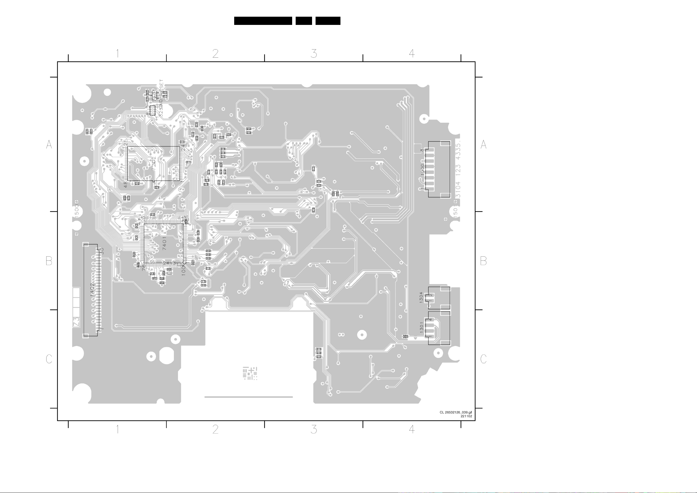
Electrical Diagrams and Print-Layouts
Layout Servo Board 43353 (Top Side)
32VAE8015 / 8020 7.
1000 A4
1301 C4
1304 B4
1402 B1
2116 A3
2125 B2
2202 A1
2207 A1
2208 A2
2218 A2
2219 A2
2221 A2
2222 A2
2223 A2
2224 A2
2225 A2
2226 A2
2227 A2
2228 A2
2229 A2
2230 A2
2231 A2
2232 A2
2233 A2
2234 A2
2315 C3
2402 B1
2405 B2
2413 B2
2422 B1
2423 B1
2424 B1
2425 B1
2426 B1
2427 B2
2428 B2
2430 B2
2431 B2
2432 B1
2446 B2
2447 A1
3121 A3
3122 A3
3130 B2
3216 A1
3217 A1
3246 A2
3250 A2
3251 A2
3252 A2
3259 A1
3264 A3
3265 A3
3274 A1
3275 A2
3277 A1
3325 C3
3328 C3
3370 C4
3408 B1
3409 B1
3463 B2
3468 B2
3469 B2
3471 A1
4203 A1
4205 A1
4210 A3
4400 A2
5202 A2
5401 B1
7201 A1
7202 A1
7401 B1
Page 33

Electrical Diagrams and Print-Layouts
Layout Servo Board 43353 (Bottom Side)
33VAE8015 / 8020 7.
1100 B3
1200 A2
1201 A2
1202 A3
1203 A4
1300 C1
1302 B1
1303 A1
1401 B4
2002 A1
2003 B1
2004 A1
2005 A1
2008 A2
2009 A1
2010 A1
2011 A1
2012 A1
2013 A1
2014 A2
2015 A1
2016 A1
2017 A1
2018 A2
2019 A1
2020 A1
2100 A2
2101 B3
2102 A3
2104 A3
2105 A3
2106 A3
2110 A2
2111 B3
2121 B2
2122 B2
2126 B2
2127 B2
2200 A3
2203 A4
2209 A2
2210 A2
2211 A3
2212 A3
2214 A3
2220 A3
2300 C2
2301 B1
2302 C2
2303 C2
2304 C2
2305 C2
2309 B3
2310 C1
2311 B3
2312 B3
2313 B2
2314 C1
2316 C2
2317 B3
2318 C1
2319 B2
2320 B1
2321 B1
2322 B1
2323 B1
2324 B1
2325 B3
2326 B3
2327 B3
2328 B3
2329 A2
2331 B1
2332 C1
2333 C1
2334 C1
2335 B2
2336 B2
2337 B2
2338 B2
2339 C1
2400 B3
2401 B3
2406 B3
2407 B3
2408 B3
2409 B3
2414 B3
2415 C4
2416 C4
2417 B4
2418 B4
2419 B4
2420 B4
2421 B4
2429 B4
2434 B3
2435 B4
2436 B4
2437 B4
2438 B4
2439 B4
2440 B4
2441 B4
3005 A1
3006 A1
3100 A3
3101 B3
3102 B3
3103 A2
3105 B3
3107 B2
3108 B2
3114 B3
3115 B3
3129 A2
3131 B2
3132 B2
3200 A4
3201 A4
3203 A4
3204 A4
3205 A4
3210 A3
3214 A4
3220 A4
3221 A3
3222 A3
3224 A3
3225 A3
3226 A4
3227 A3
3231 A4
3235 A4
3236 A4
3237 A3
3238 A2
3241 A3
3244 A3
3245 A3
3249 A3
3253 A2
3254 A2
3255 A2
3256 A2
3257 A2
3258 A2
3260 A3
3261 A3
3262 A3
3266 A3
3267 A4
3268 A4
3269 A2
3270 A2
3271 A2
3272 A3
3276 A4
3300 B2
3302 B2
3303 B2
3304 B2
3305 C2
3307 C1
3308 B2
3309 B2
3310 C2
3311 C2
3312 C2
3313 C2
3314 B2
3315 B2
3316 B2
3317 B1
3318 B2
3319 B1
3320 A3
3321 B3
3323 A3
3324 B2
3326 B2
3327 B1
3329 C2
3330 A3
3331 B2
3332 B2
3335 C1
3336 B1
3337 B1
3338 A3
3339 B1
3340 B2
3341 A3
3342 B1
3343 A3
3344 B2
3345 A3
3346 A2
3347 A2
3348 A2
3351 B2
3352 B2
3353 B1
3354 C1
3355 C1
3356 C1
3357 C1
3358 C1
3359 C1
3361 C2
3362 C1
3364 A2
3365 A2
3366 B2
3367 B2
3368 B2
3369 B2
3400 A4
3401 B3
3407 B3
3410 B3
3415 B4
3416 B4
3417 B4
3418 A4
3419 B4
3420 B4
3430 B4
3431 B4
3439 B3
3440 B3
3448 C4
3449 B4
3450 B4
3451 A4
3461 B3
3470 B3
4000 B1
4001 A1
4201 A4
4202 A3
4206 A4
4209 A3
4300 B1
4301 B2
4305 C2
4306 C1
5100 A2
5102 A3
5104 B3
5201 A3
5300 C2
5301 C2
5302 B1
5400 B3
5402 B3
6301 C1
7000 A2
7001 A2
7101 B3
7200 A4
7203 A3
7204 A4
7205 A3
7301 C2
7302 B2
7304 B1
7306 A1
7308 C1
7309 C1
7310 C1
7311 C1
7312 C1
7402 B4
Page 34

Electrical Diagrams and Print-Layouts
34VAE8015 / 8020 7.
Personal Notes: Personal Notes:
Page 35

Alignments
8. Alignments
No alignments necessary
9. Circuit Descriptions, Abbreviation List, and Data Sheets
EN 35VAE8015 / 8020 8.
Index of this chapter:
1. Introduction
2. Block diagram
3. DVD-Mechanism
4. Optical Pickup Unit
5. Printed Wiring Board
6. Abbreviation list
7. IC Data Sheets
9.1 Introduction
The Video Engine consist of a DVD-Mechanism with dual laser
Optical Pickup Unit (OPU), a tray loader with fan unit and a
PWB containing all electronics to control the module. The
electronics of the module is responsible for all basic servo
tasks. It reads from and writes data onto the disc.
9.2 Block Diagram
LOADER
Tilt Motor
M M
L1+, L1L2+, L2-
ROHM ROHM
Tilt Motor Driver
BA5944FP
TOC
TOS
TTEN
Disc Motor
Disc Motor Driver
BA6665FM
SPIDRE
SIGNAL
PROCESSOR
Tray Sense
Tray Motor
M
11P 4P4P1303 1300 1301 1302
U,V,W coil
U+,UV+,VW+,WHall+,Hall-
TACHO1
TACHO2
TACHO3
TZA1031
7101
TR+
TR-
PCS-
pre_amp
SINH
COSPH
REFSIN
REFCOS
FEN
REN
TLN
MIRN
TILTN
PW
A1,2
CALF
XDN
PCS
+SIN, -SIN
+COS, -COS
ROHM
Sledge
offset
RFN/RFB
PCS
TRAYSW
M
8P
SL-
SL+
Servo Driver
BA5938FM
73027306 7301 7304
ACT-EMFP
ACT-EMFN
RAC-SW
ADC
flash
ADC
DAC
FOC+
FOC-
RAD+
RAD-
RFP
RFN
PPN
LASP
PD1
PD2
Q1..Q6
laser 650nm
IIC
EPLD
EPM3032AT
C44-10
scan
SAA7830
7203
Actuator
RADIAL
FOCUS
RA
SL
FO
TRAYIN
TRAYOUT
MACE 3
SERVO & uP
The PWB is a high tech module (multi layer, full SMC) with very
high component density. Despite of this, it is designed in such
a way, that repair on component level still is possible. Detailed
diagnostics and fault finding is possible via ComPair.
Some specifications:
• Record DVD+RW
– Loss less linking
– Recording speed: 1.2 x
• Playback DVD
– DVD+R(W), DVD (SL/DL), DVD-R, DVD-RW (V1.1)
– Playback speed: 1.2 x
• Playback CD
– CD-DA, CD-R, CD-RW, CD-ROM, VCD/SVCD
– Playback speed: 3 x
FS diode
EFMCLKP
EFMCLKN
EFMDATAP
EFMDATAN
MEN
CE1
FWRN,PSEN-U
DA[0..7]
UA[0..19]
650nm PD
TZA1032 TZA1030
LADIC
Micro
IIC
OSTR
FTC
IRQn
TSDEN
tilt sensor
DA[0..7]
ALE
RD-U
WR-U
INT_HDR65
CS_HDR65
MOTOR
OPU64
TZA1030
DROPPI
multibus 0-11
780nm LDGU+OPIC
IIC
EEprom
OPU Flex 45p
1100
VBIAS
SAA7831
7402
HDR 65
ENCODER/DECODER
SIDA
SICL
SILD
WOBBLE PROCESSOR
AWESOME
7401
SRAM
32k
7204
Flash Rom
7202
ADC
moto1,moto2
DATA-IN
DATA-OUT
V4
FLAG
SYNC
PPNO
RFP,RFN
RF-REF
PPNO
BCA
STAB
M
-5V
MEN
Fan
control
7312
2P1304
FAN_IN
IIS
SIDA
SICL
SILD
S2B
RXD
TXD
SUR
CPR
AIRQn
ARESETn
DLOAD
+12V
PGND
3V3
4V3
+5V
-5V
GND
3V3
to OPU64
APPLICATION
1402
1000
POWER
4V6
3V3
7001
MONO BOARD
Figure 9-1 Block diagram Basic Engine
CL 26532126_003 .eps
081102
Page 36

EN 36 VAE8015 / 80209.
Circuit Descriptions, Abbreviation List, and Data Shee ts
This section describes briefly the functional behaviour of the
engine. It performs all basic servo functions:
• It reads data from the disc,
• It writes data to the disc,
• It controls all other functions like tray control, start/stop the
disc, tracking, jumping, and communication to the host.
9.2.1 Initialisation process
After power-up or reset, a self-test will automatically start.
9.2.2 Starting up the drive
After the internal initialisation process has been finished, the
engine will wait for the first S2B user command. E.g.
“Tray_out".
9.2.3 Disc recognition process
The process of disc recognition when a disc is loaded is entirely
performed within the engine. Information about the disc type is
send to the MPEG application (back-end).
9.2.4 Write / Read process
Depending on the disc loaded and actions to be performed,
Record, Play, Search, etc. a specific sequence of commands is
executed depending on the implementation of the application.
9.2.5 Shock behaviour during recording
Shock recovery during recording is performed by the
application if the shock was too large to be absorbed by the
engine. If the engine detects unacceptable servo behaviour,
the laser will go into low power mode to protect overwriting of
neighbour tracks. This action is signalised by the internal
engine controller and reported to the application. The
application can react on this with a shock recovery procedure.
9.2.6 Function overview VAE801x and MPEG application
The VAE801x performs all basic servo functions. It reads data
from the disc and writes data to the disc, and controls all other
functions like tray control, start/stop the disc, tracking, jumping,
and communication to the host.
9.3 DVD-Mechanism
The DVD-M has an optical pickup unit (OPU) consisting of two
lasers, one for CD with a wavelength of 780 nm, and one for
DVD with a wavelength of 650 nm.
The TZA1032 (LADIC) controls the data from these lasers, and
the supply to them.
9.4 Optical Pickup Unit
Figure 9-3 Optical Pickup Unit (OPU)
The OPU 64 (Optical Pickup Unit) consists of the following
components:
•DVD+RW Optics.
• High-power red laser.
• Tilt sensor.
• Flexible connections.
• LADIC: Laser Driver IC.
• DROPPI: DVD Rewritable OPU Pre-Processor IC.
• EEPROM with OPU adjustment data.
OPU-64 Flex foil pinning specifications:
• 45 pins.
• Actuator signals: Rad +/-, Foc +/-
• Pre-processed signals.
• PPN: normalized, balanced PP output.
• RFP, RFN, RFB: differential RF output.
• Clocks: OPC-strobe, EFMClk-N/P, SCL.
• Data: EFMData-N/P, SDA.
• Power supplies:
– +3V3E: ‘clean’ power supply for LADIC
– +5V, -5V: for DROPPI
• TSDEN: tilt sensor power
•V
: Laser bias voltage (~ -1.5 V)
BIAS
CL 26532126_004.eps
081102
9.4.1 DROPPI
The DROPPI (DVD Rewritable OPU Pre-Processor IC) is a
multi-purpose analogue pre-processor IC for use in the OPU of
an optical bit engine. The device supports many photo detector
configurations and output signal modes for RF and servo
signals.
Some features of the DROPPI:
• Two inputs:
– Current: DVD photo-diode.
– Voltage: CD PDIC.
• Only one wideband signal across flex foil:
– RF (differential signal).
• Other signals have relatively low bandwidth:
– Wobble signal.
Figure 9-2 DVD-M assy
CL 26532126_005.eps
081102
– Servo signals.
Page 37

Circuit Descriptions, Abbreviation List, and Data Sheets
EN 37VAE8015 / 8020 9.
9.4.2 LADIC
The LADIC (Laser Driver IC, type number TZA1032) fulfils
three main functions:
• It drives the laser with a sequence of programmable write
strategy pulses with high timing accuracy and high peak
current levels.
• It encodes the input modulated data to a sequence of write
strategy pulses. This encoding is flexible with respect to
input modulation code (EFM, EFM+, 17 pp, etc.). The write
strategy is programmable with high flexibility for CD-R/RW
and DVD-R/RW. For this purpose the TZA1032 includes
two Random Access Memories (RAM) which can be
loaded (non real-time) via the I2C-bus from microcontroller.
• It controls the exact light power levels coming from the
laser and controls the exact power absorbed by the disc
during recording.
The TZA1032 features three independent power supplies.
These are the analogue and digital power supplies and a local
power supply for the laser driver function. The supplies can be
delivered separately to obtain maximum output performance of
the TZA1032 in environments with large and highly dynamic
current flows.
Some features of the LADIC:
• Single IC.
• Simple interface (EFM(+) Decoder, WSG, I2C
Programming).
• Black-box laser.
• Temperature compensation.
• Dynamic power level control (“Alpha” control, OPC).
• Multi-application.
– Highly programmable (control and write strategy),
– Wide driver & frequency range.
• Under 500 mW dissipation in IC.
9.5 Printed Wiring Board
OPU64
LADIC
650 nm
DROPPI
WRITE
WOBBLE
SPIDRE
PPN
RF
REN, FEN,..,
PP
RF
Q1..Q6
TS1, TS2
T
Figure 9-4 Signal path
9.5.1 SPIDRE
The SPIDRE (Signal Processing IC for Dvd REwritable) is a
multi purpose analogue pre-processor IC specifically intended
for writing applications. Its main task is normalisation of the
servo signals that go to the MACE3 servo processor (signals
like 'focus servo', 'radial servo', 'track loss servo', and 'tilt
sensor').
It is possible to optimise the dynamic range of this pre-amp/
processor combination for the LF servo and RF data paths. The
gain in both channels is separately programmable. This will
guarantee an optimal playability for all kind of discs.
The SPIDRE is optimised to work with the optical pick-up unit
pre-processor IC TZA1030 (DROPPI) and decoder IC HDR65.
AWESOME
AD
SERVO
clock
data
HDR65
READ
MACE3
CL 26532126_002 .eps
I2S
to
Datapath
081102
Some features of the SPIDRE:
• A “Writer add-on”.
• Double-Writer prepared (both CDR/RW and DVDRW).
• Direct connection to HDR65/MACE3.
• High Performance:
– 16 x DVD-ROM read.
– 64 x CD-ROM read.
– 16 x CDR/RW write.
– 4 x DVD+RW write.
• Normalisation of servo signals.
• Programmable RF gain and AGC functionality.
• Separate push-pull signal (with own AGC).
• Three wire serial interface for programming of the device
by a decoder IC or microcontroller.
9.5.2 MACE3 Servo and microprocessor
The MACE3 IC (Mini All Cd Engine, type number is SAA7830)
is a combined servo processor and micro controller (80C51).
See also the internal block diagram at the end of this chapter.
The servo front-end
The servo processor handles the signals for focusing, tracking,
and access, but also generates the control signals for the
loader block.
In a CD/DVD system, there are several control loops active.
Some of them are needed to adjust the servo error signals
(once per disc rotation). It also adjusts offsets, signal
amplitudes, and loop gains (AGCs), to enlarge system
robustness and to avoid expensive potentiometer adjustments
in production.
The other loops determine the laser spot position on the disc in
the radial, axial (focus), and tangential directions. It also has to
take care that the spot accesses a required position as fast as
possible. This access system consists of two parts, namely the
actuator and the sled, which are (within a certain range)
mechanically and electrically independent. Therefore, during
an access, the servo has to control as well the actuator as the
sled.
The analogue signals from the diode pre-processor are
converted into a digital representation using A/D converters.
The digital codes are then applied to logic circuitry to obtain the
various control signals.
PCS (Position Control Sledge)
The PCS module is used to get fast sledge access. To achieve
this, it is important that the sledge motor can rotate as fast as
possible. But of course there is a limit to this maximum
rotational speed. In order to let the sledge move even faster the
ratio of the gearing can be reduced. However, if this ratio gets
too low, the cogging/detent torque of the sledge motor will push
the laser 'off track'.
There is a solution to this: Hold the sledge motor in its position
by controlling the voltage on the motor continuously.
PCS is implemented in the following way:
A normal DC motor is used, combined with hall sensors. A DC
sled motor has a magnetic ring mounted around the shaft.
Above this magnetic ring are two hall sensors positioned 90
degrees apart. The two hall outputs, which go to the PCS
control block, are 'sin phi' and 'cos phi'. The system tries to
minimise the phase difference between the measured hall sine/
cosine inputs and a reference sin/cosine waveform.
When the sledge is in tracking, the sin/cosine wave is constant,
so the sledge is kept at its current position. When after a while,
the radial actuator drifts away, the capture point crawls a bit
further on the hall sine. So the PCS makes a micro-step. When
doing an access the servo processor keeps on stepping the
sine/cosine table, thus generating a sine/cosine wave, which
the sledge will follow.
OPC (Optimum Power Calibration)
This device has an integrated Optimum Power Calculation
block for use in CD-R, CD-RW, and DVD-RAM applications. It
Page 38

EN 38 VAE8015 / 80209.
Circuit Descriptions, Abbreviation List, and Data Shee ts
reads three analogue signals (A1, A2 and CALF), representing
Max, Min, and Average values of the EFM signal respectively.
It also takes the Power (PW) signal from the laser controller
and then feeds an analogue signal (ALPHA0) out to control the
laser power. The conversion frequency is 88KHz per channel.
Basically, the OPC procedure tries to find out the optimum
laser power to be used on a specific disc. It consists of three
phases:
1. WRITE - Random EFM data is written to the test area of the
disc at increasing levels of laser power (controlled by
ALPHA0).
2. READ - The data on A1, A2, and CALF is read back from
the test area and stored in memory.
3. CALCULATION - the embedded 8051 then calculates the
setting of ALPHA0 where the least jitter is encountered.
Some pre-processing is carried out by the OPC logic to
reduce the processor’s load.
This sequence is done twice - first a coarse calibration,
followed by a fine-tuning.
The microprocessor
multi
bus
(5 lines)
S2B
Flash
ROM
AWESOME
HDR65
fast serial bus
fast serial bus
SPIDRE
CL 26532126_001.eps
to
Datapath
081102
OPU64
LADIC
DROPPI
EEPROM
MACE3
I2C
8-bit parallel bus
Figure 9-5 Control path
The micro controller processes the S2B commands from the
DVD+RW interface (back-end), and controls the various
processes in the OPU via I2C. Communication with the
HDR65, SPIDRE, and memories is done via an eight bit
parallel bus.
Some features:
• Dedicated hardwired DSP.
• 8051-based microprocessor.
• External Flash ROM and SRAM memory.
The demodulator part detects the frame synchronisation
signals and decodes the EFM (14 bit) and EFM+ (16 bit) data
and sub-code words into 8-bit symbols. Via the serial output
interface, the I2S data (audio and video) go to the DVD+RW
interface (back-end).
The spindle-motor interface provides both motor control signals
from the demodulator and, in addition, contains a tachometer
loop that accepts tachometer pulses from the motor unit. They
drive the motor IC (item 7301).
The SAA7831 has two independent microcontroller interfaces.
The first is a serial I2C-bus and the second is a standard 8-bit
multiplexed parallel interface. Both of these interfaces provide
access to 32 8-bit registers for control and status.
Some HDR65 features:
• Playback speeds up to 48 x CD and 8 x DVD; recording up
to 8 x CD and 4 x DVD
• Matched filter with digital equalizer, noise filter, and digital
PLL.
• EFM and EFM+ modulator and demodulator.
• Decoding, de-interleaving, and error correction according
to CD and DVD standards.
• Wobble processing for DVD-R(W) and CD.
• Motor control for CAV and CLV regulation on both recorded
and unrecorded discs.
• Automated encode start/stop mechanism, supporting bitaccurate linking (only DVD).
• Write data/clock interface compatible with LADIC.
• Versatile serial input/output interface for different formats.
• 8 bit parallel data input/output interface.
9.5.4 AWESOME
The AWESOME gate array chip (uPD65882, item 7401) is a
fully digital DVD+RW add-on for the HDR65. A combination of
both ICs can do CD and DVD decoding and CD, DVD-R(W),
and DVD+RW encoding. It contains logic for:
• Wobble processing:
– Address detection,
– Write clock generation,
– Start and stop.
• ADIP decoding.
• Spindle motor control to do CLV on wobble.
• Link bits insertion (according to DVD+RW standard).
• Output to SPIDRE pre-processor for wobble-AGC
It also contains multiplexing logic for the motor signals and a
merge of the internal serial bus to the analogue pre-processor
(SPIDRE) with the serial bus of the HDR65.
Note: AWESOME stands for: Adip decoding, Wobble
processing, Error correction, Synchronous start/stop and
Occasionally Mend Errors.
9.5.3 HDR65
The HDR65 has the following functions:
• Encoder for DVD+RW. This part creates the EFM+ (16 bit)
signals from the I2S data stream.
• Decoder for DVD and CD. This part processes the HF-
signal from the SPIDRE. It converts the EFM(+) signals to
data, and performs error detection and error correction.
• Output to SPIDRE pre-processor for RF-AGC.
This IC decodes EFM or EFM+HF signals directly from the
laser pre-amplifier, including analogue front-end, PLL data
recovery, demodulation, and error correction.
The analogue front-end input converts the HF input to the
digital domain via an 8-bit ADC, preceded by an AGC circuit to
obtain the optimum performance from the converter. An
external resonator clocks this block. This subsystem recovers
the data from the channel stream. It corrects asymmetry,
performs noise filtering and equalisation, and finally recovers
the bit clock and data from the channel using a digital PLL.
Wobble
land
mark
(data)
CL 26532126_020.eps
(Re)Writable Disk
wobbled
pregroove
laser
beam
Figure 9-6 Pre-groove wobble on (re)writable discs
empty
track
written
track
251102
Page 39
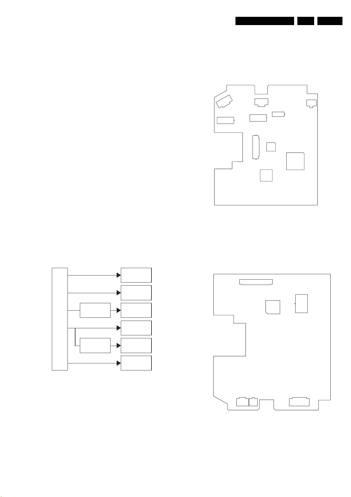
Circuit Descriptions, Abbreviation List, and Data Sheets
EN 39VAE8015 / 8020 9.
All recordable DVD media types feature a microscopic wobble
groove embedded in the plastic substrate. This wobble
provides the recorder with the timing information needed to
place the data accurately on the disc. During recording, the
drive's laser follows this groove, to ensure consistent spacing
of data in a spiral track. The walls of the groove are modulated
in a consistent sinusoidal pattern, so that a drive can read and
compare it to an oscillator for precise rotation of the disc. This
modulated pattern is called a wobble groove, because the walls
of the groove appear to wobble from side to side. This signal is
only used during recording, and therefore has no effect on the
playback process. Among the DVD family of formats, only
recordable media use wobble grooves.
For lossless linking it is necessary to write any data block in the
correct position with high accuracy (within
1 micron). For this purpose the groove is mastered with a high
wobble frequency (817 kHz at n=1), which
ensures that the writing can be started and stopped at an
accurately defined position. The writing clock as
obtained from this groove is very accurate. At the same time,
address information is stored in this wobbled
groove by locally inverting the sign of the wobbled waveform.
Some characteristics:
• Only exists on (re)writable media.
• Pregroove wobble-detector present in recorders.
• Pregroove wobble-detector not present in players.
• Wobble-frequency is different for different standards:
– DVD+R(W): 820 kHz
– DVD-R(W), DVD-RAM: 141 kHz
• The wobble is phase modulated by inverting wobble
cycles.
• The information contained in the wobble modulation is
called Address-in-Pregroove or ADIP.
9.5.5 Power Supply
+12V
+5V
+4V6
+3V3
REGULATOR
FAN
DRIVER ICs
SPIDRE
OPU
OPU
program will receive a reset, and the data of the Flash ROM is
copied into the uP-RAM.
When the MACE IC is reset, also the HDR65 (SAA7831, item
7402) and AWESOME (uPD65882, item 7401) will get a reset
via the 'SYS-RSTn', an output signal from the MACE.
9.5.6 PWB connections
1100
7302
1302
7306
7101
7203
7402
CL 26532126_007.eps
1300
7301
Figure 9-8 A-side connections
• OPU-64: 45 pins flex foil (item 1100).
• Disk motor and hall elements: 11 pins flex foil (item 1300).
• Sledge motor and hall output: 8 pins flex foil (item 1302).
• Tilt motor: 4 pins flex foil (item 1303).
1402
7401
7202
1303
191102
-5V
(POWER SUPPLY)
MODULE INTERFACE
V
BIAS
REGULATOR
+3V3
SPIDRE
OPU
OPU
MACE3
HDR65
AWESOME
CL 26532126_006.eps
081102
Figure 9-7 Power supply overview
The main power supplies to the module are 3.3 V, 5 V, and 12
V (input via connector 1000).
The MACE3, HDR65, and AWESOME ICs use the 3.3 V.
An on-board linear regulator is used to generate the -1.5 V
required by the laser (V
). The other on-board linear
BIAS
regulator is used to generate the 3V3E required by the OPU.
The SPIDRE and OPU use the +5 V and -5 V. The motor, fan,
and servo drivers use the 12 V.
Power 'on' reset
At power 'on', a reset IC (AMD810, item 7201) generates a
positive reset pulse of typicac 240 ms. As a result, the micro
1301 1304 1000
CL 26532126_008.eps
191102
Figure 9-9 Z-side connections
• Tray motor: 4 pins wired (item 1301).
• Fan: 2 pins wired (item 1304).
• Digital PWB (back-end): 30 pins flex foil (item 1402).
• Power supply: 8 pins wired (item 1000).
Page 40

EN 40 VAE8015 / 80209.
Circuit Descriptions, Abbreviation List, and Data Shee ts
9.6 Abbreviation list
ADC Analogue to Digital Converter
ADIP ADdress In Pre-groove
AGC Automatic Gain Control
CD Compact Disc
CLV Constant Linear Velocity
DROPPI Dvd Rewritable Opu Pre-Processor IC
AM Amplitude Modulation
BE Basic Engine
ComPair Computer aided rePair
CD-DA CD Digital Audio
CS Chip Select
DAC Digital to Analogue Converter
DAIO Digital Audio Input Output
DENC Digital Encoder
DFU Direction For Use: description for the
end user
DNR Dynamic Noise Reduction
DRAM Dynamic RAM
DSD Direct Stream Digital
DSP Digital Signal Processing
DVD Digital Versatile Disc
EEPROM Electrical Erasable Programmable
ROM
EFM Eight to Fourteen bit Modulation
FDS Full Diagnostic Software
HF High Frequency
I2C Integrated Ic bus (signals at 5V level)
I2S Integrated Ic Sound bus (signals at
3.3V level)
IC Integrated Circuit
IF Intermediate Frequency
IRQ Interrupt ReQuest
LADIC LAser Driver IC
LLD Loss Less Decoder
LPCM Linear Pulse Code Modulation
LRCLK Left/Right CLocK
MACE Mini All Cd Engine
MPEG Motion Pictures Experts Group
NC Not Connected
NVM Non Volatile Memory: IC containing
DVD related data e.g. alignments
OPC Optimum Power Calibration
OPU Optical Pickup Unit
PCB Printed Circuit Board (see PWB)
PCS Position Control Sledge
PLL Phase Locked Loop
PCM Pulse Code Modulation
PCM_CLK Audio system clock for DAC
PCM_OUTx Audio serial output data
PSU Power Supply Unit
PWB Printed Wiring Board (see PCB)
RAM Random Access Memory
RGB Red, Green and Blue colour space
ROM Read Only Memory
RF Radio Frequency
S2B Serial to Basic engine, communication
bus between host- and servo
processor
SCL Serial Clock I2C
SCLK Audio serial bit clock
SDA Serial Data I2C
SDRAM Synchronous DRAM
SMC Surface Mounted Components
S/PDIF Sony Philips Digital InterFace
SPIDRE Signal Processing Ic for Dvd
REwritable
SRAM Static Random Access Memory
STBY STandBY
SVCD Super Video CD
SW SoftWare
THD Total Harmonic Distortion
TTL Transistor Transistor Logic (5V logic)
uP Microprocessor
VCD Video CD
Y/C Luminance (Y) and Chrominance (C)
signal
YUV Component video
Page 41

Circuit Descriptions, Abbreviation List, and Data Sheets
9.7 IC Data Sheets
In this paragraph, the internal block diagrams and pinning are
given of ICs that are drawn as a 'black box' in the electrical
diagrams (with the exception of 'memory' and 'logic' ICs).
9.7.1 Diagram 2, SAA7830 (IC7203)
VRIN
D1_TILTN
D2_TLN
D3_REN
D4_FEN
S1_MIRN
S2_Pw
IREFT
FTCh
FTCl
CALF
SINPHI
COSPHI
XDET
ACTEMFP
ACTEMFN
UREF
UOPB
ALPHA0
DEB_OUT
MON_A
MON_D
SCCLK
OSCIN
OSCOUT
A1
A2
PW
Servo
Front-end
OPC/PCS
Front-end
Debug
interface
Clock
PLL
Test
Digital Servo
PCS
OPC
80C51
MicroRAM 736
AuxRAM 1k5
SDA
SCL
SRV_int_LGR
OPC_int
FOK
CLO
TEN
TPWM
RA
FO
SL
DSDEN
OTD
RP
TL_FTL
DEFI
DEFOn
LLP
LDON
P1.0/Int2_home
P1.1/Int3_ALEh
P1.2/PXT2E
P1.3/PXT2
P1.4/PXT0
P1.5/PXT1
P1.6/WRnh
P1.7/RDnh
P4.0/H0/A16
P4.1/H1/A17
P4.2/H2/CE1
P4.3/H3/CE2
P4.4/H4
P4.5/H5
P4.6/H6
P4.7/H7
EN 41VAE8015 / 8020 9.
TEST1
TEST2
ATEST
RxD1
TxD1
INT0
INT1
RxD2
TxD2
WRn
RDn
Figure 9-10 Internal Block Diagram MACE3
1
2
3
4
5
6
7
8
9
10
11
12
13
14
15
16
17
18
19
20
21
22
23
24
25
26
27
28
29
30
31
32
33
34
35
36
nc1
nc2
PCODE
TEST1
TEST2
ATEST
CRIN
CROUT
nc3
IREF
Vssaop
Vddaop
SINPHI
COSPHI
auxPw
XDN
ACT_EMFP
ACT_EMFN
A1
A2
CALF
UREF
Uopb
ALPHA0
Vssas
Vddas
D1_TILTN
D2_TLN
D3_REN
D4_FEN
S1_MIRN
S2_PW
VRIN
FTCh
FTCl
nc4
144
nc11
143
nc10
142
EWN
CE3
140
139
141
138T1137
136
135
CE2
CE1
Vss3P1
Vdd3P1
RWN_BOOTS
130
129
133
132
131
Vss3P7
INT_HDR65
scclk
Vdd3P7
128
deb_out
134
INT_PLUM
LOW_ADDR
MACE3
A8-15
127
mon_A
mon_D
ALE
EAn
AD0-7
PSENn
123
126
125
124
122
121
OTD
PORE
Vss3C3
Vdd3C3
INTERN
120
LLP
118
119
ATIP_in
HRESET
CL 26532126_013.eps
117
115
116
P3.2_INT0
P3.1_TXD1
P3.0_RXD1
113
114
Vss3P6
Vdd3P6
P3.3_INT1
081102
110
111
112
P3.5_TXD2
P3.4_RXD2
109
nc9
P3.6_WRn
P3.7_RDn
SRSTn
EAN_WAITN
ALE_ASTB
Vss3P5
Vdd3P5
UDA7
UDA6
UDA5
UDA4
UDA3
UDA2
UDA1
UDA0
Vss3C2
Vdd3C2
UA0_P1.0
UA1_P1.1
UA2_P1.2
UA3_P1.3
UA4_P1.4
UA5_P1.5
UA6_P1.6
UA7_P1.7
PSENN_CS
Vss3P4
Vdd3P4
UA8
UA9
UA10
UA11
UA12
UA13
nc8
108
107
106
105
104
103
102
101
100
99
98
97
96
95
94
93
92
91
90
89
88
87
86
85
84
83
82
81
80
79
78
77
76
75
74
nc7
73
nc5
37
39
38
P5.4_FOK_RP
P5.5_TL_FTL
P5.6_DEFIN
P5.7_DEFON
42
41
40
Vdd3P2
43
44
Vss3P2
P5.3
45
P5.1_SDA
P5.2_CLO
46
P5.0_SCL
49SL48RA47
52
Figure 9-11 Pinning MACE3
STEP_A0
TOSTOC_EN
TOC51TOS50FO
55
54
53
REFSIN
RAC_SW
57
56
REFCOS
Vdd3C1
59
58
P4.6_PXT2
P4.7_PXT2EN
Vss3C1
62
61
60
Vdd3P3
P4.4_PXT1
P4.5_PXT0
65
64
63
Vss3P3
67
66
P4.2_A18
P4.3_A19
68
P4.1_A17
71
nc6
UA1470UA1569P4.0_A16
72
CL 26532126_012.eps
191102
Page 42

EN 42 VAE8015 / 802010.
10. Spare Parts List
Spare Parts List
Miscellaneous
Various
0000 7104 099 28362 SUB CHASSIS 8 TEST CD
0000 7104 099 91691 MPTD PRINTED TEST DISC
0000 7104 099 97941 MPTD PRINTED TEST DISC
0000 7104 099 91041 BURN-IN TEST DISC DL
0000 7104 099 97931 MPTD THIN TEST DISC
0000 7104 099 98502 NLT 01.00 LINK TEST DISC
0000 7104 099 98582 BLANK DVD+RW DISC
0000 7104 099 91041 BLANK DVD+R DISC
CVP02.1
CVP02.1
LVP04.15
CVP02.60
DVDRO
RICOH
RICOH
Mechanical Parts
Various
0001 3104 147 17471 LOADER ASSY
0100 9305 022 82001 DVDM/01, LADIC
0100 9305 022 82002 DVDM/02, LADIC
0100 9305 022 82003 DVDM/03, LADIC
0011 3104 148 01780 FAN
0104 3104 144 06540 SUSPENSION
0105 3104 144 06540 SUSPENSION
0106 3104 144 06540 SUSPENSION
0107 3104 144 06540 SUSPENSION
0108 3104 140 40650 DVDM MOUNTING SCREW
0109 3104 140 40650 DVDM MOUNTING SCREW
0110 3104 140 40650 DVDM MOUNTING SCREW
0111 3104 140 40650 DVDM MOUNTING SCREW
0000 3104 144 07200 TILT GEAR
0000 3104 141 23380 TILT BLADE SPRING
0000 3104 148 01520 TILT MOTOR ASSY
0000 3104 147 17481 SLEDGE MOTOR ASSY
0034 3104 148 01960 LOADING TRAY MOTOR
0000 3104 144 07244 OPU RACK SLEDGE
0000 3104 141 22833 OPU RACK SPRING
0000 3104 157 12392 OPU FLEX
0002 3104 128 08262 PCB ASSY VAE8010, 8015
0002 3104 128 08322 PCB ASSY VAE8020/02/03
M3,OPU6464.3 EU
M3,OPU6464.4 US
M4,OPU6410.1
Electrical Parts
Various
0000 2422 025 17276 S2B CONNECTOR
1100 2422 025 17751 CON BM H 45P F 0.5 FFC
1201 2422 540 98428 RESONATOR 8.467MHz
1300 4822 267 51454 CONN. 11P FEMALE
1302 2422 025 16158 CON BM H 8P F 1.00 FFC
1303 2422 025 17427 CON BM H 4P F 1.00 FFC
1401 2422 540 98428 RESONATOR 8.467MHz
1402 2422 025 17276 CON BM H 30P F 1.00 FFC
2002 5322 126 11583 10nF 10% 50V 0603
2003 4822 124 23002 10µF 16V
2004 5322 126 11583 10nF 10% 50V 0603
2005 4822 124 23002 10µF 16V
2008 5322 126 11583 10nF 10% 50V 0603
2009 4822 124 23002 10µF 16V
2010 5322 126 11583 10nF 10% 50V 0603
2011 4822 124 23002 10µF 16V
2012 5322 126 11583 10nF 10% 50V 0603
2013 4822 124 23002 10µF 16V
2014 4822 124 12084 1µF 20% SM 50V
2015 2238 586 59812 0603 50V 100NP80M
2016 4822 124 23002 10µF 16V
2017 5322 126 11583 10nF 10% 50V 0603
2018 2238 586 59812 0603 50V 100NP80M
0.3 R
0.3 R
0.3 R
SMT R
2019 4822 124 23002 10µF 16V
2020 2238 586 59812 0603 50V 100NP80M
2100 2238 586 59812 0603 50V 100NP80M
2101 5322 126 11583 10nF 10% 50V 0603
2102 2238 586 59812 0603 50V 100NP80M
2104 5322 126 11583 10nF 10% 50V 0603
2105 5322 126 11583 10nF 10% 50V 0603
2106 4822 122 33735 27nF 10% 63V
2110 2238 586 59812 0603 50V 100NP80M
2111 2238 586 59812 0603 50V 100NP80M
2116 2238 586 59812 0603 50V 100NP80M
2121 5322 126 11579 3.3nF 10% 63V
2122 5322 126 11582 6.8nF 10% 63V
2125 5322 126 11583 10nF 10% 50V 0603
2127 5322 126 11583 10nF 10% 50V 0603
2200 2238 586 59812 0603 50V 100NP80M
2202 2238 586 59812 0603 50V 100NP80M
2203 4822 124 23002 10µF 16V
2207 3198 017 44740 0603 10V 470nF COL
2208 2238 586 59812 0603 50V 100NP80M
2209 2238 586 59812 0603 50V 100NP80M
2210 2238 586 59812 0603 50V 100NP80M
2211 2238 586 59812 0603 50V 100NP80M
2212 5322 126 11583 10nF 10% 50V 0603
2214 2238 586 59812 0603 50V 100NP80M
2218 2238 586 59812 0603 50V 100NP80M
2219 2238 586 59812 0603 50V 100NP80M
2220 2238 586 59812 0603 50V 100NP80M
2221 2238 586 59812 0603 50V 100NP80M
2222 2238 586 59812 0603 50V 100NP80M
2223 2238 586 59812 0603 50V 100NP80M
2224 2238 586 59812 0603 50V 100NP80M
2225 2238 586 59812 0603 50V 100NP80M
2226 2238 586 59812 0603 50V 100NP80M
2227 2238 586 59812 0603 50V 100NP80M
2228 2238 586 59812 0603 50V 100NP80M
2232 2238 586 59812 0603 50V 100NP80M
2233 4822 122 33753 150pF 5% 50V
2234 4822 122 33753 150pF 5% 50V
2300 5322 126 11583 10nF 10% 50V 0603
2301 4822 124 23002 10µF 16V
2302 3198 017 34730 0603 16V 47nF COL
2303 3198 030 74780 EL SM 35V 4U7 PM20 COL
2304 5322 126 11583 10nF 10% 50V 0603
2305 4822 124 23002 10µF 16V
2309 3198 016 31020 0603 25V 1nF
2310 3198 016 31020 0603 25V 1nF
2311 4822 126 14494 22nF 10% 25V 0603
2312 2238 786 11554 0603 16V 2N2 PM5 R
2313 2238 586 59812 0603 50V 100NP80M
2314 3198 016 31020 0603 25V 1nF
2315 2238 586 59812 0603 50V 100NP80M
2316 2238 586 59812 0603 50V 100NP80M
2317 5322 126 11583 10nF 10% 50V 0603
2318 3198 016 31020 0603 25V 1nF
2319 2238 586 59812 0603 50V 100NP80M
2320 3198 016 31020 0603 25V 1nF
2321 3198 016 31020 0603 25V 1nF
2322 2238 586 59812 0603 50V 100NP80M
2323 4822 126 14494 22nF 10% 25V 0603
2324 5322 124 41945 22µF 20% 35V
2325 2238 586 59812 0603 50V 100NP80M
2326 3198 017 31530 0603 50V 15nF COL R
2327 2238 586 59812 0603 50V 100NP80M
2328 3198 017 31530 0603 50V 15nF COL R
2329 2238 586 59812 0603 50V 100NP80M
2331 2238 586 59812 0603 50V 100NP80M
2332 2238 586 59812 0603 50V 100NP80M
2333 5322 124 41945 22µF 20% 35V
2334 2238 586 59812 0603 50V 100NP80M
2335 2238 786 11554 0603 16V 2N2 PM5 R
2336 3198 017 34730 0603 16V 47nF COL
2337 3198 017 34730 0603 16V 47nF COL
2338 2238 786 11554 0603 16V 2N2 PM5 R
2339 4822 124 23002 10µF 16V
2400 4822 124 23002 10µF 16V
2401 5322 126 11583 10nF 10% 50V 0603
2402 2238 586 59812 0603 50V 100NP80M
2405 2238 586 59812 0603 50V 100NP80M
2406 2238 586 59812 0603 50V 100NP80M
2407 2238 586 59812 0603 50V 100NP80M
2409 2238 586 59812 0603 50V 100NP80M
2413 2238 586 59812 0603 50V 100NP80M
2414 2238 786 11554 0603 16V 2N2 PM5 R
2421 4822 122 33761 22pF 5% 50V
2422 2238 586 59812 0603 50V 100NP80M
2423 2238 586 59812 0603 50V 100NP80M
2424 2238 586 59812 0603 50V 100NP80M
R
2425 2238 586 59812 0603 50V 100NP80M
2426 2238 586 59812 0603 50V 100NP80M
2427 2238 586 59812 0603 50V 100NP80M
2428 2238 586 59812 0603 50V 100NP80M
2429 2238 586 59812 0603 50V 100NP80M
2430 2238 586 59812 0603 50V 100NP80M
2431 2238 586 59812 0603 50V 100NP80M
2432 2238 586 59812 0603 50V 100NP80M
2434 4822 122 33741 10pF 10% 50V
2435 4822 122 33761 22pF 5% 50V
2436 4822 122 33761 22pF 5% 50V
2437 4822 122 33761 22pF 5% 50V
2438 4822 122 33761 22pF 5% 50V
2439 4822 122 33761 22pF 5% 50V
2440 4822 122 33761 22pF 5% 50V
2441 4822 122 33761 22pF 5% 50V
2446 5322 126 11583 10nF 10% 50V 0603
2447 2238 586 59812 0603 50V 100NP80M
3000 4822 051 30479 47Ω 5% 0.062W
3005 4822 051 30121 120Ω 5% 0.062W
3006 2322 704 64309 RST SM 0603 RC22H 43Ω
3100 4822 051 30103 10k 5% 0.062W
3101 4822 051 30103 10k 5% 0.062W
3103 5322 117 13029 47k 1% 0.063W 0603 RC22H
3105 4822 051 30681 680Ω 5% 0.062W
3107 4822 051 30101 100Ω 5% 0.062W
3108 4822 051 30101 100Ω 5% 0.062W
3114 4822 051 30101 100Ω 5% 0.062W
3115 4822 051 30101 100Ω 5% 0.062W
3121 4822 051 30681 680Ω 5% 0.062W
3122 4822 051 30152 1k5 5% 0.062W
3129 4822 051 30154 150k 5% 0.062W
3130 4822 051 30101 100Ω 5% 0.062W
3132 4822 117 12917 1Ω 5% 0.062W CASE0603
3200 4822 051 30103 10k 5% 0.062W
3201 4822 051 30103 10k 5% 0.062W
3204 4822 117 12917 1Ω 5% 0.062W CASE0603
3205 4822 051 30103 10k 5% 0.062W
3210 4822 117 13573 NETW 4 X 47Ω 5% MNR14
3214 4822 051 30103 10k 5% 0.062W
3216 4822 051 30103 10k 5% 0.062W
3217 4822 051 30103 10k 5% 0.062W
3221 4822 051 30472 4k7 5% 0.062W
3222 4822 051 30103 10k 5% 0.062W
3224 4822 051 30105 1M 5% 0.062W
3225 4822 051 30331 330Ω 5% 0.062W
3226 4822 117 13573 NETW 4 X 47Ω 5% MNR14
3227 4822 117 13525 24k 1% 0.62W RC22H 0603
3231 4822 117 13573 NETW 4 X 47Ω 5% MNR14
3235 4822 051 30103 10k 5% 0.062W
3236 4822 051 30103 10k 5% 0.062W
3237 4822 051 30223 22k 5% 0.062W
3238 4822 051 30222 2k2 5% 0.062W
3241 4822 051 30103 10k 5% 0.062W
3244 4822 051 30103 10k 5% 0.062W
3245 4822 051 30472 4k7 5% 0.062W
3246 4822 051 30479 47Ω 5% 0.062W
3249 4822 051 30103 10k 5% 0.062W
3250 4822 051 30479 47Ω 5% 0.062W
3251 4822 051 30222 2k2 5% 0.062W
3252 4822 051 30222 2k2 5% 0.062W
3253 4822 051 30273 27k 5% 0.062W
3254 4822 051 30273 27k 5% 0.062W
3255 4822 051 30273 27k 5% 0.062W
3256 4822 051 30273 27k 5% 0.062W
3257 4822 051 30273 27k 5% 0.062W
3258 4822 051 30273 27k 5% 0.062W
3259 4822 117 13573 NETW 4 X 47Ω 5% MNR14
3260 4822 117 13573 NETW 4 X 47Ω 5% MNR14
3261 4822 051 30103 10k 5% 0.062W
3262 4822 117 11817 1k2 1% 1/16W
3264 4822 117 13632 100k 1% 0603 0.62W
3265 4822 117 13632 100k 1% 0603 0.62W
3266 4822 051 30103 10k 5% 0.062W
3267 4822 051 30103 10k 5% 0.062W
3268 4822 051 30103 10k 5% 0.062W
3269 4822 051 30102 1k 5% 0.062W
3270 4822 051 30102 1k 5% 0.062W
3271 4822 051 30102 1k 5% 0.062W
3272 4822 051 30103 10k 5% 0.062W
3274 4822 051 30103 10k 5% 0.062W
3275 4822 051 30103 10k 5% 0.062W
3276 4822 051 30103 10k 5% 0.062W
3277 4822 051 30102 1k 5% 0.062W
3300 4822 051 30272 2k7 5% 0.062W
PM1
Page 43

Spare Parts List
EN 43VAE8015 / 8020 10.
3302 4822 051 30272 2k7 5% 0.062W
3303 4822 051 30102 1k 5% 0.062W
3304 4822 051 30102 1k 5% 0.062W
3305 4822 117 13608 4.7Ω 5% 0603 0.0016W
3307 5322 117 13068 82Ω 1% 0.063W 0603
3308 4822 051 20108 1Ω 5% 0.1W
3309 4822 051 20108 1Ω 5% 0.1W
3310 4822 117 12917 1Ω 5% 0.062W CASE0603
3311 4822 117 12917 1Ω 5% 0.062W CASE0603
3312 4822 117 12917 1Ω 5% 0.062W CASE0603
3314 4822 051 20108 1Ω 5% 0.1W
3315 4822 051 20108 1Ω 5% 0.1W
3316 4822 051 20228 2Ω2 5% 0.1W
3317 4822 051 20228 2Ω2 5% 0.1W
3318 4822 051 20228 2Ω2 5% 0.1W
3319 4822 051 20228 2Ω2 5% 0.1W
3320 4822 051 30332 3k3 5% 0.062W
3321 4822 051 30563 56k 5% 0.062W
3323 4822 051 30222 2k2 5% 0.062W
3324 5322 117 13049 470Ω 1% 0.063W 0603
3325 5322 117 13049 470Ω 1% 0.063W 0603
3326 5322 117 13049 470Ω 1% 0.063W 0603
3327 4822 051 30103 10k 5% 0.062W
3328 5322 117 13049 470Ω 1% 0.063W 0603
3329 4822 117 13632 100k 1% 0603 0.62W
3330 4822 051 30332 3k3 5% 0.062W
3331 4822 051 30103 10k 5% 0.062W
3332 2322 704 62003 RST SM 0603 RC22H 20k
3335 5322 117 13068 82Ω 1% 0.063W 0603
3336 4822 117 12864 82k 5% 0.6W
3337 4822 051 30273 27k 5% 0.062W
3338 4822 051 30103 10k 5% 0.062W
3339 4822 117 12864 82k 5% 0.6W
3340 4822 051 30332 3k3 5% 0.062W
3341 4822 051 30102 1k 5% 0.062W
3342 4822 051 30273 27k 5% 0.062W
3343 4822 051 30103 10k 5% 0.062W
3344 4822 051 30332 3k3 5% 0.062W
3345 4822 051 30102 1k 5% 0.062W
3346 5322 117 13049 470Ω 1% 0.063W 0603
3347 5322 117 13049 470Ω 1% 0.063W 0603
3348 4822 117 13632 100k 1% 0603 0.62W
3351 4822 051 30472 4k7 5% 0.062W
3352 4822 051 30153 15k 5% 0.062W
3353 4822 051 30123 12k 5% 0.062W
3354 4822 117 11817 1k2 1% 1/16W
3355 4822 051 30332 3k3 5% 0.062W
3356 4822 051 30472 4k7 5% 0.062W
3357 4822 117 13632 100k 1% 0603 0.62W
3358 4822 051 30102 1k 5% 0.062W
3359 2322 704 62002 RST SM 0603 RC22H 2k
3361 4822 051 30563 56k 5% 0.062W
3362 4822 051 30103 10k 5% 0.062W
3364 4822 051 30272 2k7 5% 0.062W
3365 4822 051 30272 2k7 5% 0.062W
3367 4822 051 30471 470Ω 5% 0.062W
3369 4822 051 30471 470Ω 5% 0.062W
3370 4822 051 30103 10k 5% 0.062W
3400 4822 117 11817 1k2 1% 1/16W
3401 2350 035 10152 RST NETW SM ARV24
3407 4822 117 13525 24k 1% 0.62W RC22H 0603
3408 4822 051 30103 10k 5% 0.062W
3409 4822 051 30103 10k 5% 0.062W
3410 2350 035 10152 RST NETW SM ARV24
3415 4822 051 30101 100Ω 5% 0.062W
3416 4822 051 30105 1M 5% 0.062W
3417 4822 051 30331 330Ω 5% 0.062W
3418 4822 117 13578 4X10k 5% MNR14
3419 4822 117 13573 NETW 4 X 47Ω 5% MNR14
3420 2350 035 91001 RST NETW SM ARV24 4X
3430 4822 117 13578 4X10k 5% MNR14
3431 4822 117 13573 NETW 4 X 47Ω 5% MNR14
3439 4822 051 30109 10Ω 5% 0.062W
3440 4822 051 30109 10Ω 5% 0.062W
3448 2350 035 91001 RST NETW SM ARV24 4X
3449 4822 117 13573 NETW 4 X 47Ω 5% MNR14
3450 4822 117 13573 NETW 4 X 47Ω 5% MNR14
3451 4822 117 11817 1k2 1% 1/16W
3463 4822 051 30101 100Ω 5% 0.062W
3468 4822 051 30101 100Ω 5% 0.062W
RC22H
RC22H
RC22H
RC22H
RC22H
PM1 R
RC22H
RC22H
RC22H
PM1 R
4X1k5 PM5 R
4X1k5 PM5 R
jumper R
jumper R
3469 4822 051 30101 100Ω 5% 0.062W
3470 4822 051 30102 1k 5% 0.062W
3471 4822 117 12925 47k 1% 0.063W 0603
5100 2422 549 43303 ADJ.COIL (100µH +/-6%)
5102 2422 549 43303 ADJ.COIL (100µH +/-6%)
5104 2422 549 43303 ADJ.COIL (100µH +/-6%)
5201 2422 549 43769 IND FXD SM EMI 100mH z
5202 2422 549 43769 IND FXD SM EMI 100mH z
5300 2422 549 43769 IND FXD SM EMI 100mH z
5301 2422 549 43769 IND FXD SM EMI 100mH z
5302 2422 549 43769 IND FXD SM EMI 100mH z
5400 2422 549 43303 ADJ.COIL (100µH +/-6%)
5401 2422 549 43769 IND FXD SM EMI 100mH z
5402 2422 549 43769 IND FXD SM EMI 100mH z
30R R
30R R
30R R
30R R
30R R
30R R
30R R
6301 4822 130 11397 BAS316
7000 9322 150 89668 IC SM LM337D2T (ONSE) R
7001 9322 121 67668 IC SM LF33CD (ST00) R
7101 9352 688 06157 IC SM TZA1031HL (PHSE) Y
7200 4822 130 60373 BC856B
7201 9322 155 26685 IC SM ADM810SART
7202 9965 000 16590 FLASH FW15.07.xx
7202 9965 000 16595 FLASH FW20.09.xx
7202 9965 000 16596 FLASH FW20.01.xx
7202 9965 000 16597 FLASH FW20.02.xx
7203 9352 687 34557 IC SM SAA7830HL (PHSE) Y
7204 9322 036 99685 IC SM CY7C1399B-15ZC
7205 4822 130 60373 BC857B
7301 9322 139 85668 BA6665FM
7302 4822 209 17229 BA5938FM
7304 4822 209 30095 LM833D
7306 9322 166 66668 IC SM BA5944FP (RHM0) R
7308 9340 547 21215 FET POW SM BSH205
7309 5322 130 60159 BC846B
7310 5322 130 60159 BC846B
7311 5322 130 60159 BC846B
7312 9322 144 97668 IC SM LD1117DT (ST00) R
7401 9322 180 17671 IC SM AWESOME2 (NEC0)
7401 9322 189 16671 IC SM AWESOME3 (NEC0)
7402 9352 687 36557 IC SM SAA7831HL (PHSE) Y
(ANA0) Y
VAE8010,8015
VAE8020/01/02
VAE8020/03
VAE8020/05
(CYPR) R
(PHSE) R
Y
Y
 Loading...