

Philips UDA1361TS Datasheet

INTEGRATED CIRCUITS
DATA SH EET
UDA1361TS
96 kHz sampling 24-bit stereo
audio ADC
Product specification
File under Integrated Circuits, IC01
2001 Jan 17
Philips Semiconductors Product specification
96 kHz sampling 24-bit stereo audio ADC UDA1361TS
FEATURES
General
• Low power consumption
• 256, 384, 512 and 768fs system clock
• 2.4 to 3.6 V power supply
• Supports sampling frequency of 5 to 110 kHz
• Small package size (SSOP16)
• Integrated high-pass filter to cancel DC offset
• Power-down mode
• Supports 2 V (RMS) input signals
• Easy application
• Master or slave operation.
Multiple format output interface
• I2S-bus and MSB-justified format compatible
• Up to 24 significant bits serial output.
Advanced audio configuration
GENERAL DESCRIPTION
The UDA1361TS is a single chip stereo Analog-to-Digital
Converter (ADC) employing bitstream conversion
techniques. The low power consumption and low voltage
requirements make the device eminently suitable for use
in low-voltage low-powerportable digital audio equipment
which incorporates recording functions.
TheUDA1361TSsupportstheI2S-busdataformatandthe
MSB-justified data format with word lengths of up to
24 bits.
• Stereo single-ended input configuration
• High linearity, dynamic range and low distortion.
ORDERING INFORMATION
TYPE
NUMBER
UDA1361TS SSOP16 plastic shrink small outline package; 16 leads; body width 4.4 mm SOT369-1
NAME DESCRIPTION VERSION
PACKAGE
2001 Jan 17 2
Philips Semiconductors Product specification
96 kHz sampling 24-bit stereo audio ADC UDA1361TS
QUICK REFERENCE DATA
SYMBOL PARAMETER CONDITIONS MIN. TYP. MAX. UNIT
Supplies
V
DDA
V
DDD
I
DDA
I
DDD
T
amb
Analog
V
i(rms)
(THD + N)/S total harmonic
S/N signal-to-noise ratio V
α
cs
analog supply voltage 2.4 3.0 3.6 V
digital supply voltage 2.4 3.0 3.6 V
analog supply current fs= 48 kHz
operating mode − 10.5 − mA
Power-down mode − 0.5 − mA
digital supply current fs= 48 kHz
operating mode − 3.5 − mA
Power-down mode − 0.45 − mA
ambient temperature −40 − +85 °C
input voltage (RMS value) at 0 dB(FS) equivalent − 1.1 − V
at −1 dB(FS) signal output − 1.0 − V
fs= 48 kHz
distortion-plus-noise to signal ratio
at −1dB −−88 −83 dB
at −60 dB; A-weighted −−40 −34 dB
f
= 96 kHz
s
at −1dB −−85 −80 dB
at −60 dB; A-weighted −−40 −37 dB
= 0 V; A-weighted
i
f
= 48 kHz − 100 − dB
s
f
= 96 kHz − 100 − dB
s
channel separation − 100 − dB
2001 Jan 17 3
Philips Semiconductors Product specification
96 kHz sampling 24-bit stereo audio ADC UDA1361TS
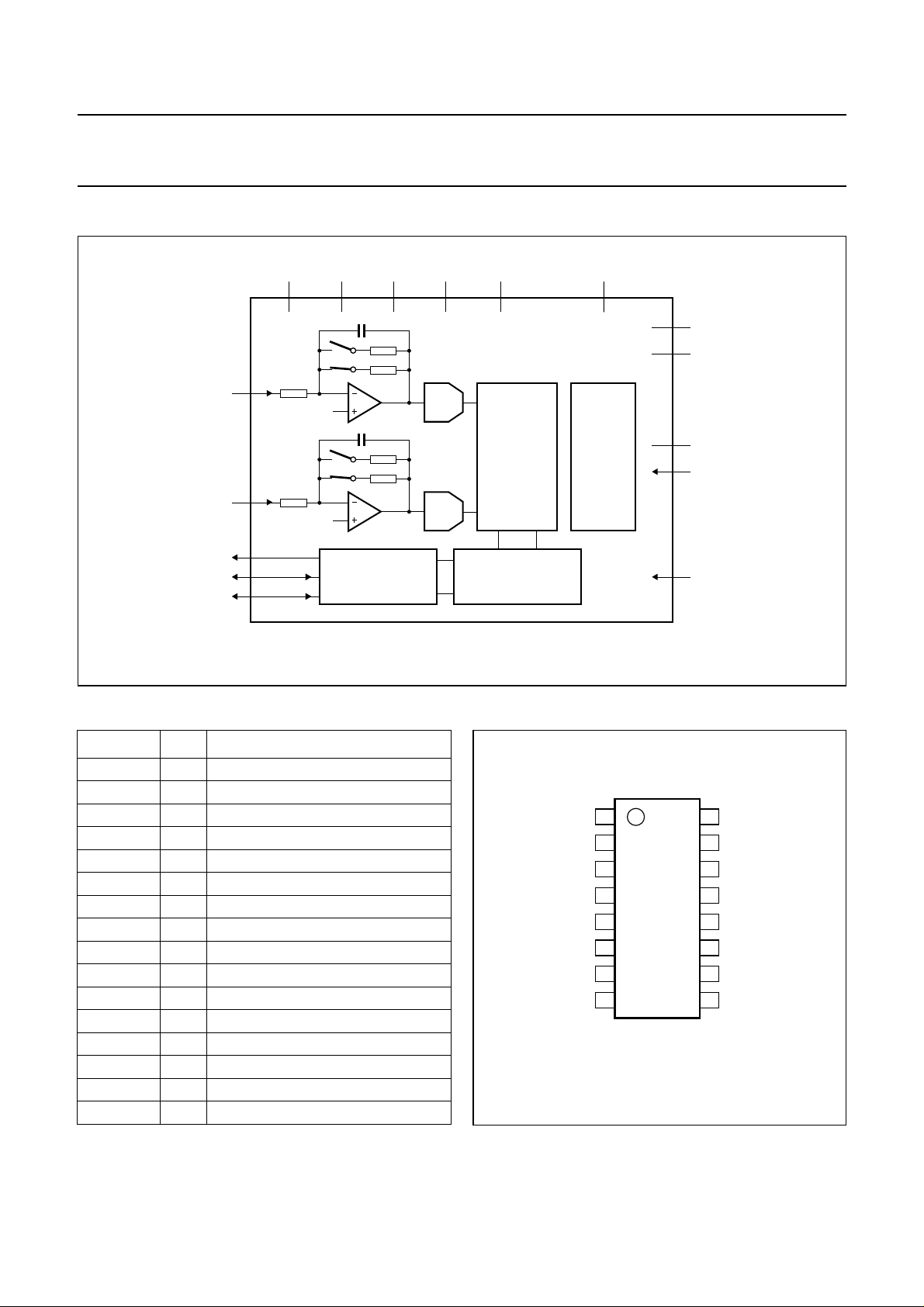
BLOCK DIAGRAM
handbook, full pagewidth
PINNING
V
INL
V
INR
DATAO
BCK
WS
DDA
V
SSA
16
V
1
3
13
11
12
V
RP
15
DIGITAL
INTERFACE
V
RN
5
ADC
Σ∆
ADC
Σ∆
V
ref
4
2
UDA1361TS
DECIMATION
FILTER
DC-CANCELLATION
FILTER
SYSCLK
8
CLOCK
CONTROL
10
14
MGT451
9
V
DDD
V
SSD
MSSEL
7
PWON
6
SFOR
Fig.1 Block diagram.
SYMBOL PIN DESCRIPTION
V
INL
V
ref
V
INR
V
RN
V
RP
1 left channel input
2 reference voltage
3 right channel input
4 negative reference voltage
5 positive reference voltage
SFOR 6 data format selection input
PWON 7 power control input
SYSCLK 8 system clock 256, 384, 512 or 768f
V
V
DDD
SSD
9 digital supply voltage
10 digital ground
BCK 11 bit clock input/output
WS 12 word select input/output
DATAO 13 data output
MSSEL 14 master/slave select
V
V
SSA
DDA
15 analog ground
16 analog supply voltage
s
handbook, halfpage
V
1
INL
V
2
ref
V
3
INR
V
4
RN
RP
UDA1361TS
5
6
7
8
V
SFOR
PWON
SYSCLK
Fig.2 Pin configuration.
MGT452
16
15
14
13
12
11
10
9
V
DDA
V
SSA
MSSEL
DATAO
WS
BCK
V
SSD
V
DDD
2001 Jan 17 4
Philips Semiconductors Product specification
96 kHz sampling 24-bit stereo audio ADC UDA1361TS
FUNCTIONAL DESCRIPTION
System clock
The UDA1361TS accommodates master and slave
modes. The system devices must provide the system
clock regardless of master or slave mode. In the master
mode a system clock frequency of 256fsis required. In the
slave mode a system frequency of 256, 384, 512 or 768f
is automatically detected (for a system clock of 768fs the
sampling frequency must be limited to 55 kHz). The
system clock must be locked in frequency to the digital
interface input signals.
Input level
The overall system gain is proportional to V
DDA
, or more
accurately the potential difference between the reference
voltages V
VRP
and V
. The −1 dB input level at which
VRN
THD + N/S is specified corresponds to −1 dB(FS) digital
output (relative to the full-scale swing). With an input gain
switch, the input level can be calculated as follows:
–
V
at 0 dB gain:
at 6 dB gain:
V
1 dB–()
i
1 dB–()
V
i
VRPVVRN
---------------------------------3
–
V
VRPVVRN
----------------------------------
23×
V (RMS)==
V (RMS)==
In applications where a 2 V (RMS) input signal is used, a
12 kΩ resistor must be connected in series with the input
of the ADC. This forms a voltage divider together with the
internal ADC resistor and ensures that only 1 V (RMS)
maximum is input to the IC.
Table 1 Application modes using input gain stage
RESISTOR
(12 kΩ)
INPUT GAIN
SWITCH
MAXIMUM
INPUT
VOLTAGE (RMS)
Present 0 dB 2 V
Present 0 dB 1 V
s
Absent 0 dB 1 V
Absent 6 dB 0.5 V
Multiple format output interface
The serial interface provides the following data output
formats in both master and slave modes
(see Figs 3, 4 and 5).
• I2S-bus with data word length of up to 24 bits
• MSB-justifiedserialformatwithdatawordlengthofupto
24 bits.
The master mode drives pins WS (word select; 1fs) and
BCK (bit clock; 64fs). WS and BCK are received in slave
mode.
Table 2 Master/slave select
MSSEL MASTER/SLAVE SELECT
L slave mode
H master mode
M (reserved for digital test)
Table 3 Select data format
Usingthisapplicationfora2 V (RMS) input signal,thegain
switch must be set to 0 dB. When a 1 V (RMS) input signal
is input to the ADC in the same application the gain switch
must be set to 6 dB.
Anoverviewofthemaximuminputvoltageallowedagainst
the presence of an external resistor and the setting of the
gain switch is given in Table . The power supply voltage is
assumed to be 3 V.
2001 Jan 17 5
SFOR DATA FORMAT
2
LI
S-bus data format
H MSB-justified data format
M (reserved for analog test)
Decimation filter
The decimation from 64fsis performed in two stages. The
first stage realizes a 4th-order sinx/x characteristic. This
filter decreases the sample rate by 8.
The second stage, a FIR filter, consists of 3 half-band
filters, each decimating by a factor of 2.
Philips Semiconductors Product specification
96 kHz sampling 24-bit stereo audio ADC UDA1361TS
Table 4 Decimation filter characteristic
ITEM CONDITION VALUE (dB)
Pass-band ripple 0 to 0.45f
Pass-band droop 0.45f
Stop band >0.55 f
S
S
Dynamic range 0 to 0.45 f
S
S
±0.01
−0.2
−70
>135
DC cancellation filter
A IIR high-pass filter is provided to remove unwanted
DC components. The filter characteristics are given in
Table 5.
Table 5 DC cancellation filter characteristic
ITEM CONDITION VALUE (dB)
Pass-band ripple − none
Pass-band gain − 0
Droop at 0.00045f
Attenuation
at 0.00000036f
S
S
−0.031
>40
at DC
Dynamic range 0 to 0.45f
S
>135
Mute
On recovery from Power-down, the serial data output
DATAO is held LOW until valid data is available from the
decimation filter. This time tracks with the sampling
frequency:
12288
=
t
, t = 256 ms when f
---------------f
s
= 48 kHz.
s
Power-down mode/input voltage control
The PWON pin can control the power saving together with
the optional gain switch for 2 or 1 V (RMS) input.
The UDA1361TS supports 2 V (RMS) input using a series
resistor of 12 kΩ. For the definition of the pin settings for
1 or 2 V (RMS) mode, it is assumed that this resistor is
present as a default component.
Table 6 Power-down/input voltage control
PWON POWER-DOWN OR GAIN
L Power-down mode
M 0 dB gain
H 6 dB gain
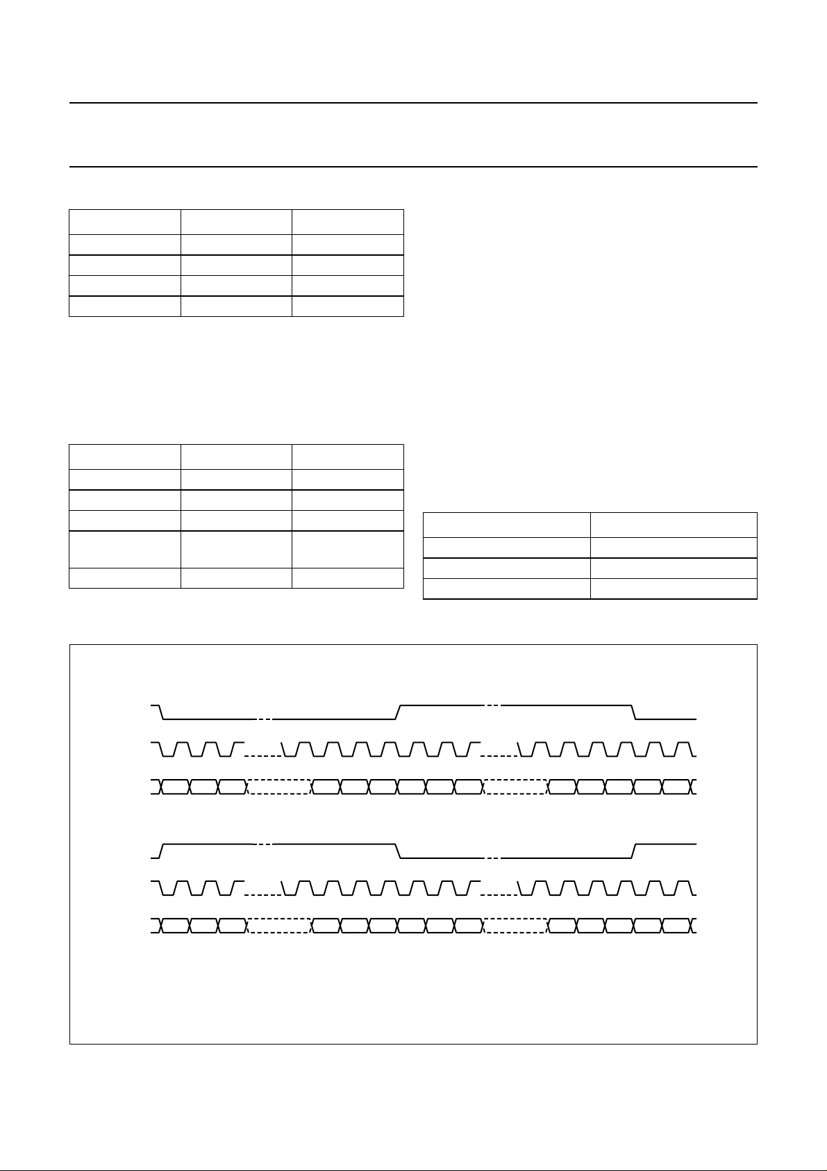
Serial interface formats
handbook, full pagewidth
WS
BCK
DATA
WS
BCK
DATA
MSB B2 MSBLSB LSB MSBB2
MSB B2 MSBLSB LSB MSB B2B2
LEFT
LEFT
RIGHT
2
S-BUS
321321
RIGHT
321321
≥8 ≥8
INPUT FORMAT I
≥8 ≥8
MSB-JUSTIFIED FORMAT
Fig.3 Serial interface formats.
MGT453
2001 Jan 17 6
 Loading...