

Philips UDA1360TS Datasheet
INTEGRATED CIRCUITS
DATA SH EET
UDA1360TS
Low-voltage low-power stereo
audio ADC
Preliminary specification
File under Integrated Circuits, IC01
1998 Oct 02
Philips Semiconductors Preliminary specification
Low-voltage low-power stereo audio ADC UDA1360TS
FEATURES
General
• Low power consumption
• 2.7 to 3.6 V power supply
• supports 256 and 384f
• Small package size (SSOP16)
• Integrated high-pass filter to cancel DC offset
• Power-down mode
• Supports 2 V (RMS) input signals
• Easy application
• Non-inverting ADC plus decimation filter.
Multiple format output interface
2
• I
S-bus and MSB-justified format compatible
• Up to 20 significant bits serial output.
Advanced audio configuration
system clock
s
GENERAL DESCRIPTION
The UDA1360TS is a single chip stereo Analog-to-Digital
Converter (ADC) employing bitstream conversion
techniques. The low power consumption and low voltage
requirements make the device eminently suitable for use
in low-voltage low-power portable digital audio equipment
which incorporates recording functions.
The UDA1360TS supports the I
2
S-bus data format and the
MSB-justified data format with word lengths of up to
20 bits.
• Stereo single-ended input configuration
• High linearity, dynamic range and low distortion.
QUICK REFERENCE DATA
SYMBOL PARAMETER CONDITIONS MIN. TYP. MAX. UNIT
Supplies
V
V
I
DDA
I
DDD
T
DDA
DDD
amb
analog supply voltage 2.7 3.0 3.6 V
digital supply voltage 2.7 3.0 3.6 V
analog supply current − 9 − mA
digital supply current − 3.5 − mA
operating ambient temperature −20 − +85 °C
ADC
V
i(rms)
(THD + N)/S total harmonic distortion plus
S/N signal-to-noise ratio V
α
cs
input voltage (RMS value) see Table 1 − 1.0 − V
at 0 dB −−85 −80 dB
noise-to-signal ratio
at −60 dB; A-weighted −−37 −33 dB
= 0 V; A-weighted − 97 − dB
I
channel separation − 100 − dB
ORDERING INFORMATION
TYPE
NUMBER
NAME DESCRIPTION VERSION
PACKAGE
UDA1360TS SSOP16 plastic shrink small outline package; 16 leads; body width 4.4 mm SOT369-1
1998 Oct 02 2
Philips Semiconductors Preliminary specification
Low-voltage low-power stereo audio ADC UDA1360TS
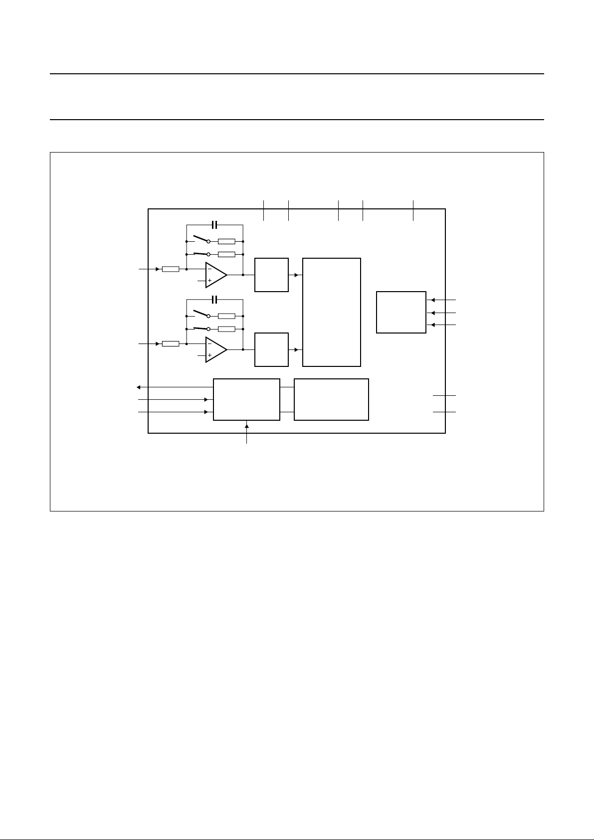
BLOCK DIAGRAM
V
handbook, full pagewidth
V
DDA
V
SSA
16
15 5 4 2
V
ref(n)
ref(p)
UDA1360TS
V
ref
VINL
VINR
DATAO
BCK
WS
1
3
13
11
12
DIGITAL
INTERFACE
SFOR
ADC
(Σ∆)
8
SYSCLK
DECIMATION
FILTER
ADC
(Σ∆)
DC-CANCELLATION
FILTER
6
CLOCK
CONTROL
14
10
MGM967
FSEL
7
PWON
9
V
DDD
V
SSD
Fig.1 Block diagram.
1998 Oct 02 3
Philips Semiconductors Preliminary specification
Low-voltage low-power stereo audio ADC UDA1360TS
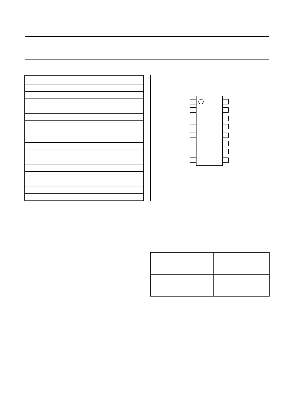
PINNING
SYMBOL PIN DESCRIPTION
VINL 1 left channel input
V
ref
VINR 3 right channel input
V
ref(n)
V
ref(p)
SFOR 6 data format selection input
PWON 7 power control input
SYSCLK 8 system clock input 256 or 384f
V
DDD
V
SSD
BCK 11 bit clock input
WS 12 word selection input
DATAO 13 data output
FSEL 14 system clock frequency select
V
SSA
V
DDA
2 reference voltage
4 ADC negative reference voltage
5 ADC positive reference voltage
9 digital supply voltage
10 digital ground
15 analog ground
16 analog supply voltage
handbook, halfpage
s
VINL
V
ref
VINR
V
ref(n)
V
ref(p)
SFOR
PWON
SYSCLK
1
2
3
4
UDA1360TS
5
6
7
8
MGM968
16
15
14
13
12
11
10
9
V
DDA
V
SSA
FSEL
DATAO
WS
BCK
V
SSD
V
DDD
Fig.2 Pin configuration.
FUNCTIONAL DESCRIPTION
System clock
The UDA1360TS accommodates slave mode only, this
means that in all applications the system devices must
provide the system clock. The system frequency is
selectable via the static FSEL pin, and the system clock
must be locked in frequency to the digital interface input
signals.
The options are 256f
(FSEL = LOW) and 384f
s
s
(FSEL = HIGH).
Analog-to-Digital Converter (ADC)
The stereo ADC of the UDA1360TS consists of two
3rd-order Sigma-Delta modulators. They have a modified
Ritchie-coder architecture in a differential switched
capacitor implementation. The over-sampling ratio is 128.
Input level
The overall system gain is proportional to V
. The 0 dB
DDA
input level is defined as that which gives a −1 dBFS digital
output (relative to the full-scale swing). In addition, an input
gain switch is incorporated with the above definitions.
The UDA1360TS front-end is equipped with a selectable
0 or 6 dB gain, in order to supports 2 V (RMS) input using
a series resistor of 12 kΩ.
For the definition of the pin settings for 1 or 2 V (RMS)
mode given in Table 1, it is assumed that this resistor is
present as a default component.
If the 2 V (RMS) signal input is not needed, the external
resistor should not be used.
Table 1 Application modes using input gain stage
RESISTOR
(12 kΩ)
INPUT GAIN
SWITCH
MAXIMUM INPUT
VOLTAGE
Present 0 dB 2 V (RMS)
Present 6 dB 1 V (RMS)
Absent 0 dB 1 V (RMS)
Absent 6 dB 0.5 V (RMS)
Multiple format output interface
The UDA1360TS supports the following data output
formats;
2
• I
S-bus with data word length of up to 20 bits
• MSB-justified serial format with data word length of up to
20 bits.
The output format can be set by the static SFOR pin. When
SFOR is LOW, the I2S-bus is selected, when SFOR is set
HIGH the MSB-justified format is selected.
1998 Oct 02 4
Philips Semiconductors Preliminary specification
Low-voltage low-power stereo audio ADC UDA1360TS
The data formats are illustrated in Fig.4. Left and right data
channel words are time multiplexed.
Decimation filter
The decimation from 128f
is performed in two stages.
s
The first stage realizes 3rd-order sinx/x characteristic. This
filter decreases the sample rate by 16. The second stage
(an FIR filter) consists of 3 half-band filters, each
decimating by a factor of 2.
Table 2 DC cancellation filter characteristics
ITEM CONDITION
VALUE
(dB)
Pass-band ripple none
Pass-band gain 0
Droop at 0.00045f
s
Attenuation at DC at 0.00000036f
Dynamic range 0 to 0.45f
s
0.031
>40
s
>110
Mute
On recovery from power-down, the serial data output
DATAO is held LOW until valid data is available from the
decimation filter. This time tracks with the sampling
frequency:
t
12288
---------------f
279 ms==
s
; where fs= 44.1 kHz.
Power-down mode
The PWON pin can control the power saving together with
the optional gain switch for 2 V (RMS) or 1 V (RMS) input.
When the PWON pin is set LOW, the ADC is set to
power-down. When PWON is set to HIGH or to half the
power supply, then either 6 dB gain or 0 dB gain in the
analog front-end is selected.
Application modes
The UDA1360TS can be set to different modes using two
3-level pins and one 2-level pin. The selection of modes is
given in Table 3.
Table 3 Mode selection summary
PIN V
SS
1
⁄2V
DD
V
DD
SFOR I2S-bus test mode MSB
PWON power-down 0 dB gain 6 dB gain
FSEL 256f
s
− 384f
s
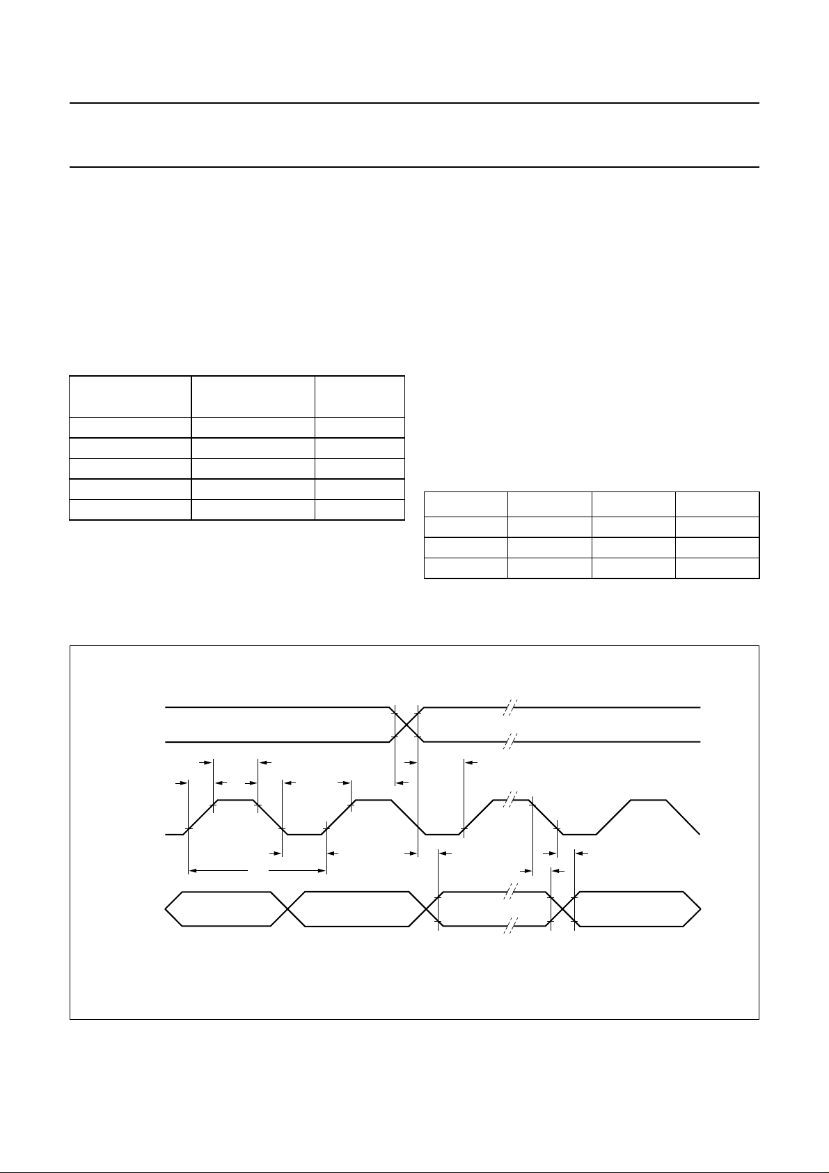
handbook, full pagewidth
WS
t
BCK(H)
t
f
t
BCK(L)
T
cy
t
h;WS
t
d;DAT(WS)
BCK
DATAO
t
r
Fig.3 Serial interface timing.
1998 Oct 02 5
t
s;WS
t
h;DAT
t
d;DAT
MGM969
 Loading...