

查询UDA1352HL供应商
INTEGRATED CIRCUITS
DATA SH EET
UDA1352HL
48 kHz IEC 60958 audio DAC
Preliminary specification
Supersedes data of 2002 May 22
2003 Mar 25

Philips Semiconductors Preliminary specification
48 kHz IEC 60958 audio DAC UDA1352HL
CONTENTS
1 FEATURES
1.1 General
1.2 Control
1.3 IEC 60958 input
1.4 Digital sound processing and DAC
2 APPLICATIONS
3 GENERAL DESCRIPTION
4 ORDERING INFORMATION
5 QUICK REFERENCE DATA
6 BLOCK DIAGRAM
7 PINNING
8 FUNCTIONAL DESCRIPTION
8.1 Operating modes
8.2 Clock regeneration and lock detection
8.3 Crystal oscillator
8.4 Mute
8.5 Auto mute
8.6 Data path
8.7 Control
9 L3-BUS DESCRIPTION
9.1 General
9.2 Device addressing
9.3 Register addressing
9.4 Data write mode
9.5 Data read mode
9.6 Initialization string
10 I2C-BUS DESCRIPTION
10.1 Characteristics of the I2C-bus
10.2 Bit transfer
10.3 Byte transfer
10.4 Data transfer
10.5 Start and stop conditions
10.6 Acknowledgment
10.7 Device address
10.8 Register address
10.9 Write and read data
10.10 Write cycle
10.11 Read cycle
11 SPDIF SIGNAL FORMAT
11.1 SPDIF channel encoding
11.2 SPDIF hierarchical layers for audio data
11.3 SPDIF hierarchical layers for digital data
11.4 Timing characteristics
12 REGISTER MAPPING
12.1 Clock settings (write)
12.2 I2S-bus output settings (write)
12.3 I2S-bus input settings (write)
12.4 Power-down settings (write)
12.5 Volume control left and right (write)
12.6 Sound feature mode, treble and bass boost
settings (write)
12.7 De-emphasis and mute (write)
12.8 DAC source and clock settings (write)
12.9 SPDIF input settings (write)
12.10 Supplemental settings (write)
12.11 PLL coarse ratio (write)
12.12 Interpolator status (read-out)
12.13 SPDIF status (read-out)
12.14 Channel status (read-out)
12.15 PLL status (read-out)
13 LIMITING VALUES
14 THERMAL CHARACTERISTICS
15 CHARACTERISTICS
16 TIMING CHARACTERISTICS
17 APPLICATION INFORMATION
18 PACKAGE OUTLINE
19 SOLDERING
19.1 Introduction to soldering surface mount
packages
19.2 Reflow soldering
19.3 Wave soldering
19.4 Manual soldering
19.5 Suitability of surface mount IC packages for
wave and reflow soldering methods
20 DATA SHEET STATUS
21 DEFINITIONS
22 DISCLAIMERS
23 PURCHASE OF PHILIPS I2C COMPONENTS
2003 Mar 25 2
Philips Semiconductors Preliminary specification
48 kHz IEC 60958 audio DAC UDA1352HL
1 FEATURES
1.1 General
• 2.7 to 3.6 V power supply
• Integrated digital filter and Digital-to-Analog
Converter (DAC)
• 256fs system clock output
• 20-bit data path in interpolator
• High performance
• No analog post filtering required for DAC
• Supported sampling frequencies of 28 up to 55 kHz.
1.2 Control
• Controlled by either static pins, I2C-bus or L3-bus
microcontroller interfaces.
• Bass boost and treble control in L3-bus or I2C-bus
modes
• Interpolating filter (fsto 64fs or 128fs) using cascaded
recursive and FIR filters
• Fifth-order noise shaper (operating either at 64f
or 128fs) generates the bitstream for the DAC
• Filter Stream DAC (FSDAC).
s
1.3 IEC 60958 input
• On-chip amplifier converts IEC 60958 input to CMOS
levels
• Lock status indication at pin LOCK
• Pulse Code Modulation (PCM) input signal status
indication at pin PCMDET
• Right and left channels each have 40 key
channel-status bits available via L3-bus or I2C-bus
interfaces.
1.4 Digital sound processing and DAC
• Automatic de-emphasis when using IEC 60958 input
with audio sample frequencies (fs) of 32.0, 44.1 and
48.0 kHz
• Soft mute using a cosine roll-off circuit selectable via
pin MUTE, L3-bus or I2C-bus interfaces
• Left and right independent dB linear volume control
having 0.25 dB steps from 0 to −50 dB, 1 dB steps to
−60, −66 and −∞ dB
4 ORDERING INFORMATION
TYPE
NUMBER
UDA1352HL LQFP48 plastic low profile quad flat package; 48 leads; body 7 × 7 × 1.4 mm SOT313-2
NAME DESCRIPTION VERSION
2 APPLICATIONS
• Digital audio systems.
3 GENERAL DESCRIPTION
The UDA1352HL is a single-chip IEC 60958 audio
decoder with an integrated stereo DAC employing
bitstream conversion techniques.
A lock status signal is available on pin LOCK, to indicate
when the IEC 60958 decoder is locked. A PCM detection
status signalis available on pin PCMDET to indicate when
PCM data is present at the input.
By default, the DAC output and the data output interface
are muted when the decoder is out-of-lock. However, this
setting can be overridden in the L3-bus or I2C-bus modes.
The UDA1352HL in package LQFP48 is the full featured
version. Also available is the UDA1352TS in package
SSOP28 which has the IEC 60958 input only to the DAC.
PACKAGE
2003 Mar 25 3
Philips Semiconductors Preliminary specification
48 kHz IEC 60958 audio DAC UDA1352HL
5 QUICK REFERENCE DATA
V
DDD=VDDA
ground; unless otherwise specified.
SYMBOL PARAMETER CONDITIONS MIN. TYP. MAX. UNIT
Supplies
V
DDD
V
DDA
I
DDA(DAC)
I
DDA(PLL)
I
DDD(C)
I
DDD
P
48
General
t
rst
T
amb
Digital-to-analog converter
V
o(rms)
∆V
o
(THD+N)/S total harmonic
S/N
48
α
cs
= 3.0 V; IEC 60958 input with fs= 48 kHz; T
=25°C; RL=5kΩ; all voltages measured with respect to
amb
digital supply voltage 2.7 3.0 3.6 V
analog supply voltage 2.7 3.0 3.6 V
analog supply current of DAC power-on − 3.3 − mA
power-down; clock off − 35 −µA
analog supply current of PLL at fs= 48 kHz − 0.5 − mA
digital supply current of core at fs= 48 kHz − 9 − mA
digital supply current at fs= 48 kHz − 0.6 − mA
power consumption at
fs=48kHz
DAC in Playback mode − 40 − mW
DAC in Power-down mode − tbf − mW
reset active time − 250 −µs
ambient temperature −40 − +85 °C
output voltage (RMS value) fi= 1.0 kHz tone at 0 dBFS; note 1 850 900 950 mV
unbalance of output voltages fi= 1.0 kHz tone − 0.1 0.4 dB
f
= 1.0 kHz tone at fs=48kHz
i
distortion-plus-noise to signal
ratio
signal-to-noise ratio at
at 0 dBFS −−82 −77 dB
at −40 dBFS; A-weighted −−60 −52 dB
fi= 1.0 kHz tone; code = 0; A-weighted 95 100 − dB
fs=48kHz
channel separation fi= 1.0 kHz tone − 110 − dB
Note
1. The output voltage of the DAC is proportional to the DAC power supply voltage.
2003 Mar 25 4
Philips Semiconductors Preliminary specification
48 kHz IEC 60958 audio DAC UDA1352HL
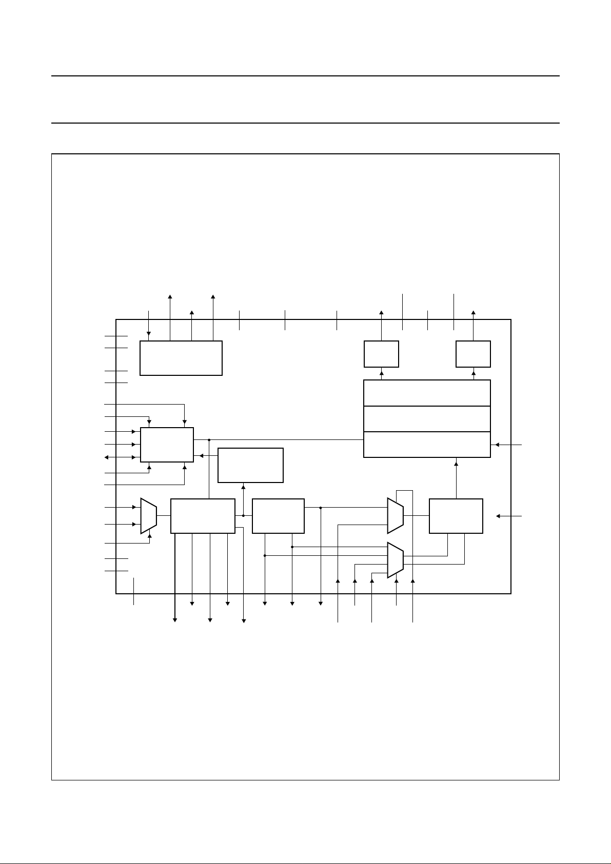
6 BLOCK DIAGRAM
handbook, full pagewidth
V
DDA(PLL)
V
SSA(PLL)
V
DDD(C)
V
SSD(C)
DA0
DA1
L3MODE
L3CLOCK
L3DATA
SELSTATIC
SELIIC
SPDIF0
SPDIF1
SELCHAN
V
DDD
V
SSD
35
34
2
4
42
37
10
6
5
38
47
16
17
14
46
3
TIMING CIRCUIT
OR I
INTERFACE
SLICER
11, 29,
30, 41, 48
n.c.
XTALOUT
CLKOUTXTALIN
1215
CLOCK
AND
L3-BUS
2
C-BUS
43
PCMDET
OSCOUT
32
IEC 60958
DECODER
23
LOCK
PREEM1
TEST
44
25
NON-PCM DATA
SYNC
DETECTOR
33
45 31
PREEM0
USERBIT
V
SSA(DACO)
UDA1352HL
DATA
OUTPUT
INTERFACE
36
BCKO
WSO
V
DDA(DACA)
V
DDA(DACO)
28
39
40
DATAO
DATAI
19
7
VOUTL
DAC
AUDIO FEATURE PROCESSOR
8
9
BCKI
WSI
V
SSA(DACA)
18
20
NOISE SHAPER
INTERPOLATOR
21
SELCLK
SELSPDIF
22
V
ref
27
26
DATA
INPUT
INTERFACE
VOUTR
24
DAC
13
MGU597
MUTE
1
RESET
Fig.1 Block diagram.
2003 Mar 25 5
Philips Semiconductors Preliminary specification
48 kHz IEC 60958 audio DAC UDA1352HL
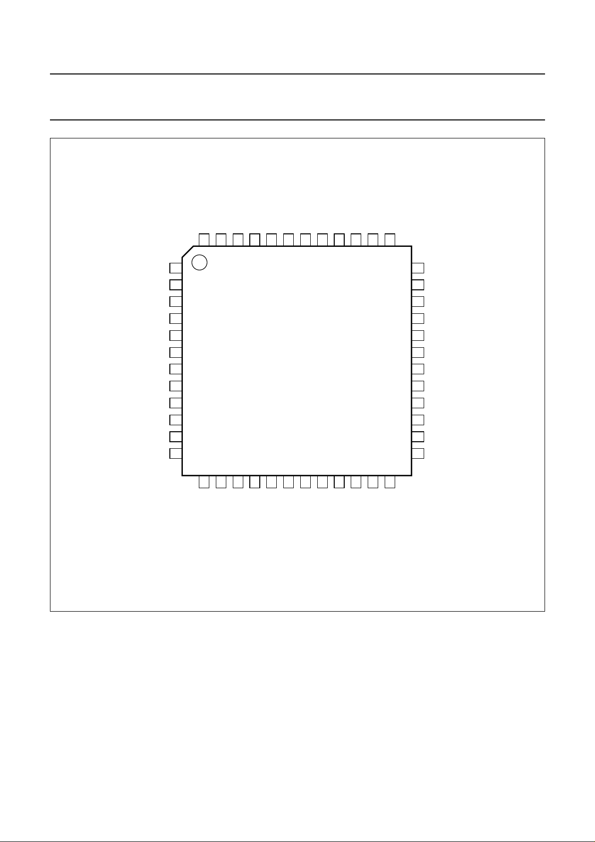
7 PINNING
SYMBOL PIN TYPE
(1)
DESCRIPTION
RESET 1 DID reset input
V
DDD(C)
V
SSD
V
SSD(C)
L3DATA 5 IIC L3-bus or I
L3CLOCK 6 DIS L3-bus or I
DATAI 7 DISD I
BCKI 8 DISD I
WSI 9 DISD I
2 DS digital supply voltage for core
3 DGND digital ground
4 DGND digital ground for core
2
C-bus interface data input and output
2
C-bus interface clock input
2
S-bus data input
2
S-bus bit clock input
2
S-bus word select input
L3MODE 10 DIS L3-bus interface mode input
n.c. 11 − not connected
XTALOUT 12 AIO crystal oscillator output
MUTE 13 DID mute control input
SELCHAN 14 DID IEC 60958 channel selection input
XTALIN 15 AIO crystal oscillator input
SPDIF0 16 AIO IEC 60958 channel 0 input
SPDIF1 17 AIO IEC 60958 channel 1 input
V
DDA(DACA)
V
DDA(DACO)
18 AS analog supply voltage for DAC
19 AS analog supply voltage for DAC
VOUTL 20 AIO DAC left channel analog output
SELCLK 21 DID clock source for PLL selection input
SELSPDIF 22 DIU IEC 60958 data selection input
LOCK 23 DO SPDIF and PLL lock indicator output
VOUTR 24 AIO DAC right channel analog output
TEST 25 DID test pin; must be connected to digital ground (V
V
ref
V
SSA(DACA)
V
SSA(DACO)
26 AIO DAC reference voltage
27 AGND analog ground for DAC
28 AGND analog ground for DAC
n.c. 29 − not connected
n.c. 30 − not connected
USERBIT 31 DO user data bit output
CLKOUT 32 DO clock output (256f
)
s
PREEM1 33 DO IEC 60958 input pre-emphasis output 1
V
SSA(PLL)
V
DDA(PLL)
BCKO 36 DO I
34 AGND analog ground for PLL
35 AS analog supply voltage for PLL
2
S-bus bit clock output
DA1 37 DISU A1 device address selection input
SELSTATIC 38 DIU static pin control selection input
DATAO 39 DO I
WSO 40 DO I
2
S-bus data output
2
S-bus word select output
) in application
SSD
2003 Mar 25 6

Philips Semiconductors Preliminary specification
48 kHz IEC 60958 audio DAC UDA1352HL
SYMBOL PIN TYPE
(1)
DESCRIPTION
n.c. 41 − not connected
DA0 42 DISD A0 device address selection input
PCMDET 43 DO PCM detection indicator output
OSCOUT 44 DO internal oscillator output
PREEM0 45 DO IEC 60958 input pre-emphasis output 0
V
DDD
SELIIC 47 DID I
46 DS digital supply voltage
2
C-bus or L3-bus mode selection input
n.c. 48 − not connected
Note
1. See Table 1.
Table 1 Pin types
TYPE DESCRIPTION
DS digital supply
DGND digital ground
AS analog supply
AGND analog ground
DI digital input
DIS digital Schmitt-triggered input
DID digital input with internal pull-down resistor
DISD digital Schmitt-triggered input with internal pull-down resistor
DIU digital input with internal pull-up resistor
DISU digital Schmitt-triggered input with internal pull-up resistor
DO digital output
DIO digital input and output
DIOS digital Schmitt-triggered input and output
IIC input and open-drain output for I
2
C-bus
AIO analog input or output
2003 Mar 25 7
Philips Semiconductors Preliminary specification
48 kHz IEC 60958 audio DAC UDA1352HL
handbook, full pagewidth
RESET
V
DDD(C)
V
SSD
V
SSD(C)
L3DATA
L3CLOCK
DATAI
BCKI
WSI
L3MODE
n.c.
XTALOUT
n.c.
48
1
2
3
4
5
6
7
8
9
10
11
12
13
MUTE
DDD
SELIIC
V
47
46
14
15
XTALIN
SELCHAN
PREEM0
OSCOUT
45
44
UDA1352HL
16
17
SPDIF0
SPDIF1
PCMDET
DA0
43
42
18
19
DDA(DACA)
DDA(DACO)
V
V
n.c.
41
20
VOUTL
WSO
DATAO
40
39
21
22
SELCLK
SELSPDIF
SELSTATIC
DA1
38
37
23
24
LOCK
VOUTR
36
35
34
33
32
31
30
29
28
27
26
25
MGU596
BCKO
V
DDA(PLL)
V
SSA(PLL)
PREEM1
CLKOUT
USERBIT
n.c.
n.c.
V
SSA(DACO)
V
SSA(DACA)
V
ref
TEST
Fig.2 Pin configuration.
2003 Mar 25 8

Philips Semiconductors Preliminary specification
48 kHz IEC 60958 audio DAC UDA1352HL
8 FUNCTIONAL DESCRIPTION
8.1 Operating modes
The UDA1352HL is a low-cost multi-purpose IEC 60958
decoder DAC with a variety of operating modes.
In operating modes 1, 2, 3, 4, 6, 7 and 8,the UDA1352HL
is the master clock generator for both the outgoing and
providing data for the UDA1352HL via the data input
interface in mode 4 will be a slave to the clock generated
by the UDA1352HL.
In mode 5 the UDA1352HL locks to signal WSI from the
digital data input interface. To conform to IEC 60958, the
audiosample frequencyofthe datainput interface mustbe
between 28 and 55 kHz.
incoming digital data streams. Consequently, any device
Table 2 Mode survey
MODE FUNCTION SCHEMATIC
1 IEC 60958 input
DAC output
SPDIF IN DAC
The system locks onto the SPDIF signal.
PLL
I2S-BUS
OUTPUT
EXTERNAL DSP
2
S-BUS
I
INPUT
XTAL
MGU598
2 IEC 60958 input
2
I
S-bus digital interface output
The system locks onto the SPDIF signal
Digital output with BCKO and WSO as
master.
SPDIF IN DAC
PLL
I2S-BUS
OUTPUT
EXTERNAL DSP
2
I
S-BUS
INPUT
XTAL
MGU599
2003 Mar 25 9
Philips Semiconductors Preliminary specification
48 kHz IEC 60958 audio DAC UDA1352HL
MODE FUNCTION SCHEMATIC
3 IEC 60958 input
I2S-bus digital interface output
DAC output
The system locks onto the SPDIF signal
Digital output with BCKO and WSO as
master.
4 IEC 60958 input
I2S-bus digital interface output
I2S-bus digital interface input
DAC output
The system locks onto the SPDIF signal
Digital output with BCKO and WSO as master
Digital input with BCKI and WSI as slave
(must be synchronized with the PLL output
clock).
SPDIF IN DAC
PLL XTAL
I2S-BUS
OUTPUT
EXTERNAL DSP
SPDIF IN DAC
PLL
I2S-BUS
OUTPUT
EXTERNAL DSP
2
S-BUS
I
INPUT
2
S-BUS
I
INPUT
MGU600
XTAL
MGU601
5I2S-bus digital interface input
DAC output
The system locks onto the WSI signal
Digital input with BCKI and WSI as slave.
2003 Mar 25 10
SPDIF IN DAC
PLL
I2S-BUS
OUTPUT
EXTERNAL DSP
2
S-BUS
I
INPUT
XTAL
MGU602
Philips Semiconductors Preliminary specification
48 kHz IEC 60958 audio DAC UDA1352HL
MODE FUNCTION SCHEMATIC
6I2S-bus digital interface input
DAC output
The crystal oscillator generates the system
clock and master clock output
Digital input with BCKI and WSI as slave.
7 IEC 60958 input
I2S-bus digital interface output
I2S-bus digital interface input
DAC output
SPDIF input to digital interface output locks
onto the SPDIF signal
DAC locks onto the crystal oscillator
Digital output with BCKO and WSO as master
Digital input with BCKI and WSI as slave
(must be synchronized with the PLL output
clock).
8 Crystal oscillator output applied to IEC 60958
input
2
I
S-bus digital interface output
SPDIF IN DAC
PLL XTAL
2
I2S-BUS
OUTPUT
EXTERNAL DSP
SPDIF IN DAC
PLL XTAL
I2S-BUS
OUTPUT
EXTERNAL DSP
SPDIF IN DAC
I
S-BUS
INPUT
2
I
S-BUS
INPUT
MGU603
MGU604
The crystal oscillator generates the master
clock
PLL regenerates BCKO and WSO from input
clock by setting the pre-scaler ratio
Digital outputwith BCKOand WSO as master
(invalid DATA)
Digital input with BCKI and WSI as slave.
2003 Mar 25 11
PLL XTAL
2
I2S-BUS
OUTPUT
I
S-BUS
INPUT
MGU605
Philips Semiconductors Preliminary specification
48 kHz IEC 60958 audio DAC UDA1352HL
8.2 Clock regeneration and lock detection
The UDA1352HL has an on-board PLL for regenerating a
system clock from the IEC 60958 input bitstream.
Remark: If there is no input signal, the PLL generates a
minimum frequency and the output spectrum shifts
accordingly. Since the analog output does not have an
analog mute, this means noise that is out of band under
normal conditions can move into the audio band.
When theon-board clocklocks to theincoming frequency,
the PLL lock indicator bit is set and can be read via the
L3-bus or I2C-bus interfaces.
By default, PLL lock status and PCM detection status
indicator signals are internally combined. Pin LOCK goes
HIGH when the IEC 60958 decoder and the on-board
clock are both locked to the incoming bitstream and if the
incoming bitstream data is PCM. However, if the IC is
locked but the incoming signal is not PCM data, or it is
burst preamble,pin LOCK goes LOW. Thecombined lock
andPCM detectionstatuscan beoverriddenby the L3-bus
or I2C-bus register bit settings.
Thelock indicationoutputsignal canbe used, forexample,
for muting purposes. It can be used to drive an external
analog muting circuit to prevent out of band noise from
becoming audible when the PLL runs at its minimum
frequency (e.g. when there is no SPDIF input signal).
Muting in these modes can only be disabled by setting
bit MT in the device register to logic 0.
A logic 1 on pin MUTE will always mute the audio output
signal in either the L3-bus or I2C-bus mode, or static pin
mode. This is in contrast to the UDA1350 and the
UDA1351 in which pin MUTE has no effect in the L3-bus
mode.
20
MGU119
t (ms)
handbook, halfpage
1
mute
factor
0.8
0.6
0.4
0.2
0
01051525
When valid PCM data is detected in the incoming
bitstream, pin PCMDET goes HIGH.
8.3 Crystal oscillator
The UDA1352HL uses an on-board crystal oscillator to
generate a clock signal. The clock signal can be used as
the internal clock, and is used directly by the DAC in
modes 6 and 7. This clock signal can also be output at
pin OSCOUT and can be applied to the SPDIF inputs.
By setting the UDA1352HL as a frequency synthesizer
(mode 8), a setof frequencies can be obtained, as shown
in Table 53.
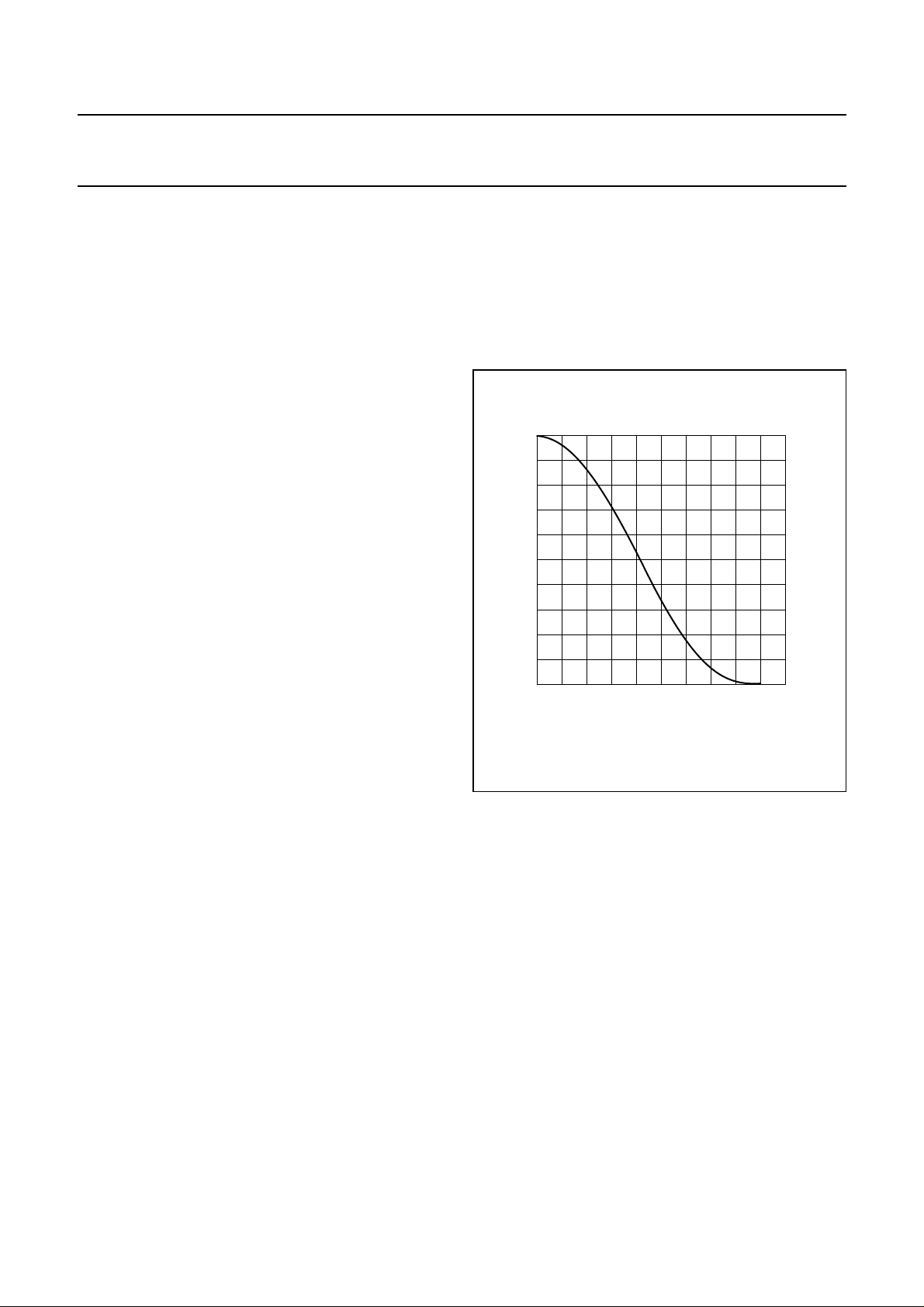
8.4 Mute
The UDA1352HL uses a cosine roll-off mute in the DSP
data path part of the DAC. Muting the DAC (by pin MUTE
or via bit MT in L3-bus or I2C-bus modes), results in a soft
mute,as showninFig.3. Thecosineroll-off softmutetakes
23 ms corresponding to 32 × 32 samples at a sampling
frequency of 44.1 kHz.
When operating in either the L3-bus or I2C-bus mode, the
device will mute the audio output on start-up by default.
Fig.3 Mute as a function of raised cosine roll-off.
2003 Mar 25 12
Philips Semiconductors Preliminary specification
48 kHz IEC 60958 audio DAC UDA1352HL
8.5 Auto mute
By default, the DAC outputs are muted until the
UDA1352HL is locked, regardless of the level on
pin MUTEor thestate of bit MT.This allowsonly valid data
to be passed to the outputs. Thismute is performed in the
SPDIF interface and is a hard mute, not a cosine roll-off
mute.
The UDA1352HL can be prevented from muting in
out-of-lock situations by setting bit MUTEBP in register
address 01H to logic 1 via the L3-bus or I2C-bus
interfaces.
8.6 Data path
The UDA1352HL data path consists of the IEC 60958
decoder, audio feature processor, digital interpolator,
noise shaper and the DACs.
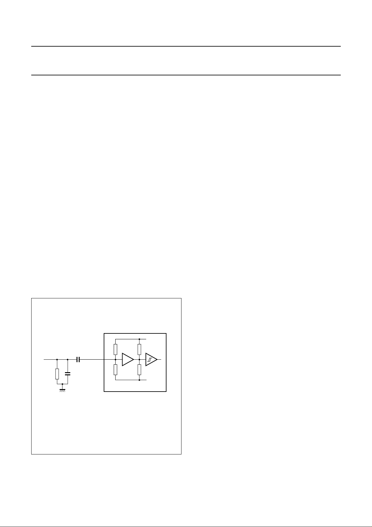
8.6.1 IEC 60958 INPUT
The IEC 60958decoder features anon-chip amplifier with
hysteresis, which amplifies the SPDIF input signal to
CMOS level (see Fig.4).
All 24 bits of data for left and right channels are extracted
from theinput bitstreamplus 40 channel-status bitsfor left
and right channels. These bits can be read via the L3-bus
or I2C-bus interfaces.
The UDA1352HL supports the following sample
frequencies and data rates:
• fs= 32.0 kHz, resulting in a data rate of 2.048 Mbits/s
• fs= 44.1 kHz, resulting in a data rate of 2.8224 Mbits/s
• fs= 48.0 kHz, resulting in a data rate of 3.072 Mbits/s.
The UDA1352HL supports timing levels I, II and III, as
specified by theIEC 60958 standard. The accuracy ofthe
above sampling frequencies depends on the timing levels
used. Timing levels I, II and III are described in
Section 11.4.1.
8.6.2 AUDIO FEATURE PROCESSOR
The audio feature processor automatically provides
de-emphasis for the IEC 60958 data stream in the static
pin control mode and default mute at start-up in either the
L3-bus or I2C-bus mode.
When usedin L3-bus or I2C-bus modes,the audio feature
processor provides the following additional features:
• Independent left and right channel volume control
• Bass boost control
• Treble control
• Selection of sound processing modes for bass boost
and treble filters: flat, minimum and maximum
• Soft mute control with raised cosine roll-off
• De-emphasis of the incoming data stream selectable at
a sampling frequency of either 32.0, 44.1 or 48.0 kHz.
handbook, halfpage
16,
17
UDA1352HL
MGU611
75 Ω
SPDIF0,
SPDIF1
10 nF
180 pF
Fig.4 IEC 60958 input circuit and typical
application.
2003 Mar 25 13
Philips Semiconductors Preliminary specification
48 kHz IEC 60958 audio DAC UDA1352HL
8.6.3 INTERPOLATOR
The UDA1352HL has an on-board interpolating filter that
convertsthe incoming datastreamfrom 1fsto 64fsor 128f
by cascading a recursive filter and a Finite Impulse
Response (FIR) filter.
Table 3 Interpolator characteristics
PARAMETER CONDITIONS VALUE (dB)
Pass-band ripple 0 to 0.45f
Stop band >0.55f
Dynamic range 0 to 0.45f
s
s
s
±0.03
−50
114
DC gain −−5.67
8.6.4 NOISE SHAPER
The fifth-order noise shaper operates either at
64fsor 128fs. It shifts in-band quantization noise to
frequencieswell abovetheaudio band.Thisnoise shaping
technique enables high signal-to-noise ratios to be
achieved. The noise shaper output is converted to an
analog signal using a filter stream DAC.
8.6.5 FILTER STREAM DAC
8.7 Control
The UDA1352HL can be controlled by static pins (when
pin SELSTATIC is HIGH), via the I2C-bus (when
s
pin SELSTATIC is LOW and pin SELIIC is HIGH) or via
the L3-bus (when pins SELSTATIC and SELIIC are
both LOW). For optimum use ofthe UDA1352HLfeatures,
theL3-bus orI2C-busmodes arerecommended since only
basic functionsare available in the static pin controlmode.
Notethat thestaticpin controlmode and L3-busor I2C-bus
modes are mutually exclusive. In the static pin control
mode, pins L3MODE and L3DATA are used to select the
format for the data output and input interface (see Fig.5).
The Filter Stream DAC (FSDAC) is a semi-digital
reconstruction filter that converts the 1-bit data stream of
the noise shaper to an analog output voltage.
The filter coefficients are implemented as current sources
andare summedatvirtual groundof the outputoperational
amplifier. In this way, very high signal-to-noise
performance and low clock jitter sensitivity is achieved.
A post filter is notneeded dueto theinherent filterfunction
of the DAC. On-board amplifiers convert the FSDAC
output current to an output voltage signal capable of
driving a line output.
The output voltage of the FSDAC is scaled proportionally
to the power supply voltage.
2003 Mar 25 14
Philips Semiconductors Preliminary specification
48 kHz IEC 60958 audio DAC UDA1352HL
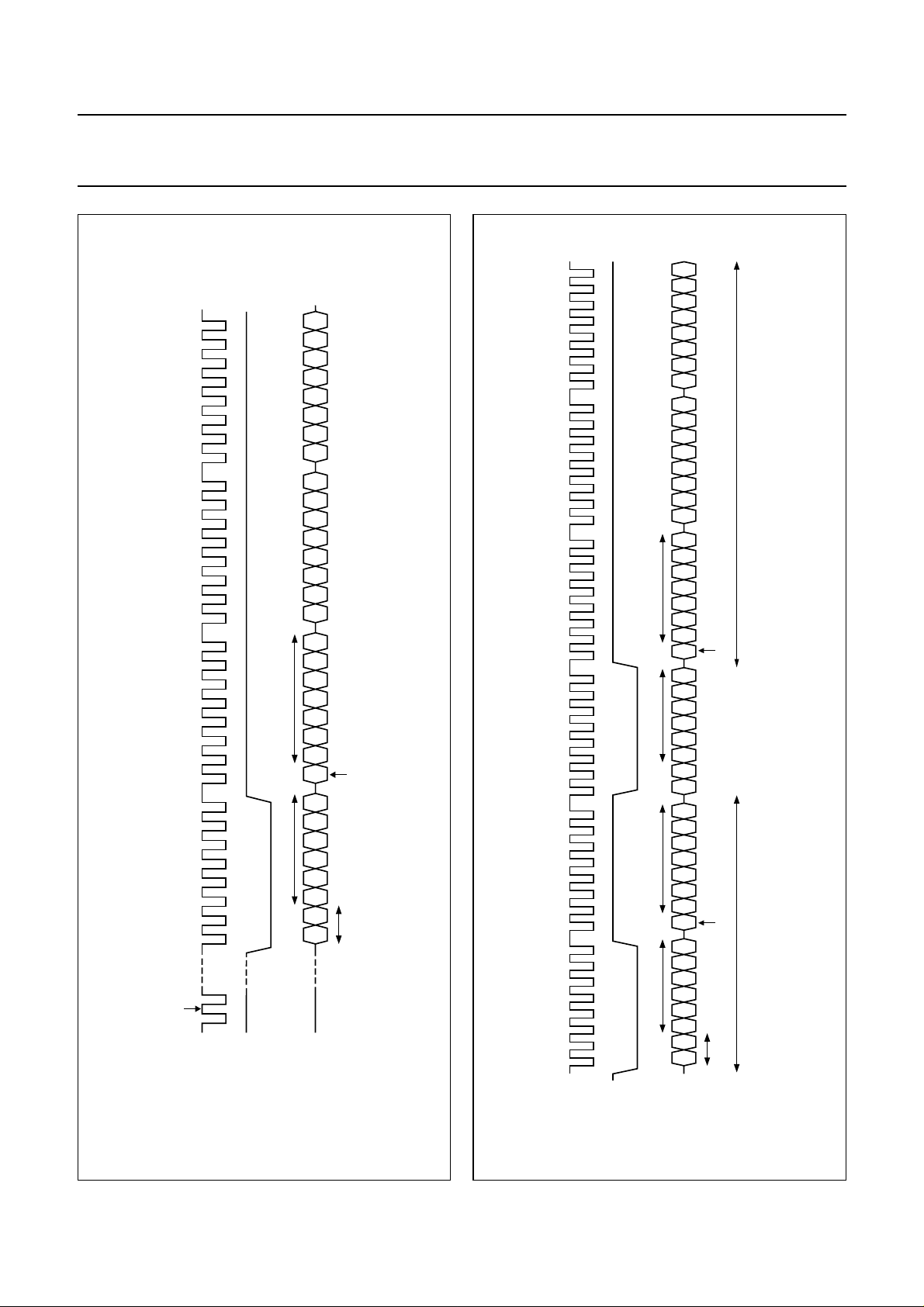
MGS752
B15 LSB
B19 LSB
B23 LSB
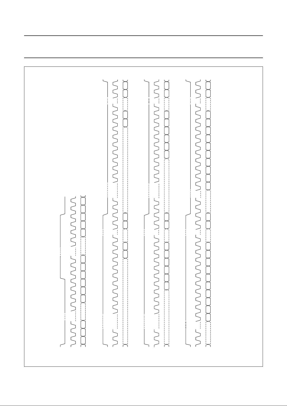
handbook, full pagewidth
RIGHT
> = 8
3
21> = 812 3
RIGHT
1518 1720 19 2 1
16
MSB B2 B3 B4 B5 B6
LSB
B19
LSB-JUSTIFIED FORMAT 20 BITS
1518 1720 19 2 1
16
15 2 1
16
MSB B2
RIGHT
LSB
B15
LSB-JUSTIFIED FORMAT 16 BITS
15 2 1
B2
16
MSB
MSB MSBB2
RIGHT
1518 1720 1922 212324 21
16
1518 1720 1922 212324 2 1
16
B5 B6 B7 B8 B9 B10
B3 B4
B2
MSB
LSB
B23
LSB-JUSTIFIED FORMAT 24 BITS
Fig.5 Digital data interface formats.
This text is here in white to force landscape pages to be rotated correctly when browsing through the pdf in the Acrobat reader.This text is here in
_white to force landscape pages to be rotated correctly when browsing through the pdf in the Acrobat reader.This text is here inThis text is here in
white to force landscape pages to be rotated correctly when browsingthrough the pdf inthe Acrobat reader. white to force landscape pages to be ...
2003 Mar 25 15
LEFT
WS
BCK
MSB B2
DATA
S-BUS FORMAT
2
I
LEFT
WS
BCK
DATA
LEFT
WS
BCK
MSB B2 B3 B4 B5 B6
DATA
LEFT
WS
BCK
B5 B6 B7 B8 B9 B10
B3 B4
B2
MSB
DATA
Philips Semiconductors Preliminary specification
48 kHz IEC 60958 audio DAC UDA1352HL
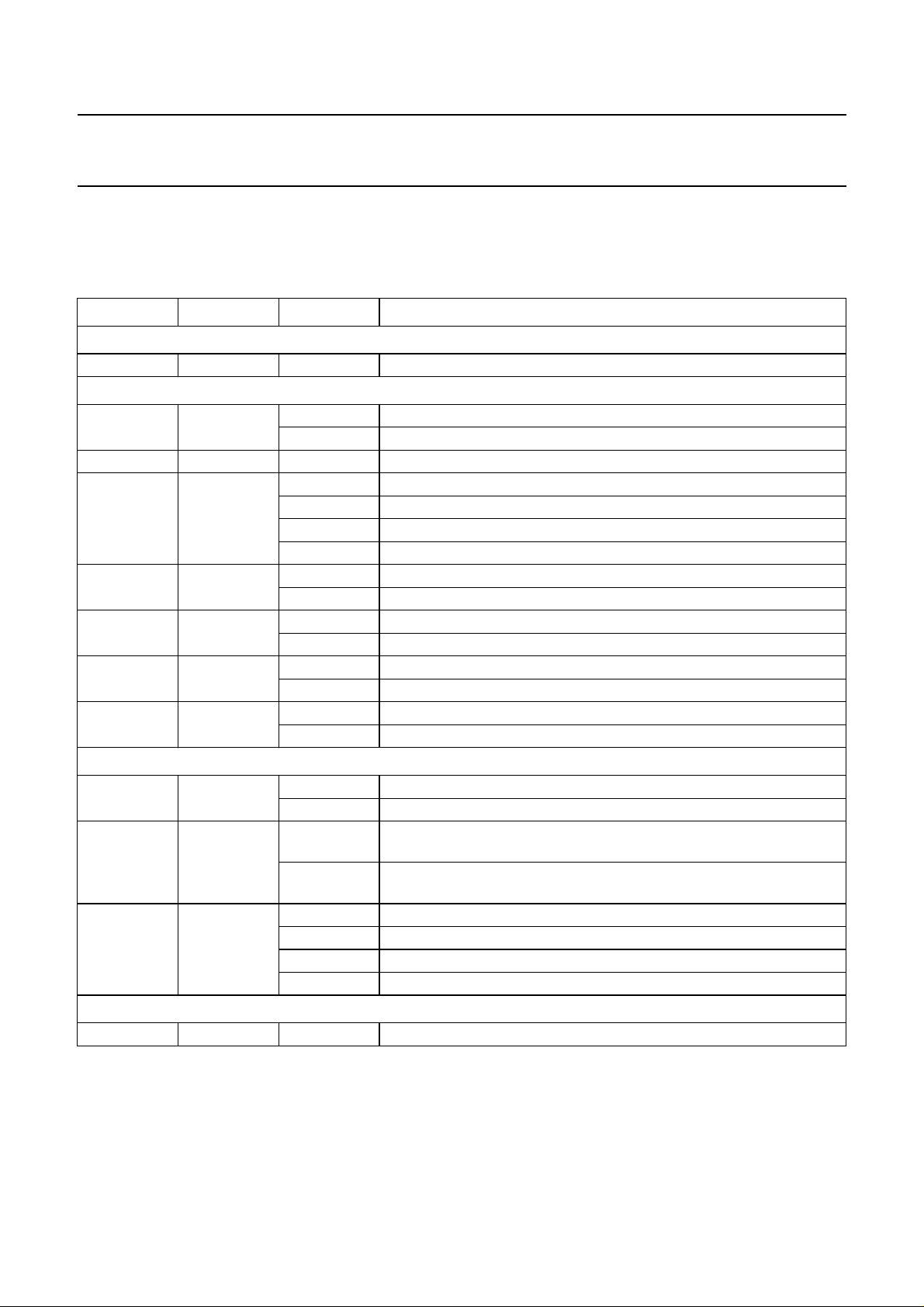
8.7.1 STATIC PIN CONTROL MODE
The functions of the static pins in static pin control mode are described in Table 4.
Table 4 Pin descriptions in static pin control mode
PIN NAME VALUE FUNCTION
Mode selection pin
38 SELSTATIC 1 select static pin control mode; must be connected to V
Input pins
1 RESET 0 normal operation
1 reset
6 L3CLOCK 0 must be connected to V
10 and 5 L3MODEand
L3DATA
00 select I2S-bus format for digital data interface
01 select LSB-justified format 16 bits for digital data interface
SSD
10 select LSB-justified format 20 bits for digital data interface
11 select LSB-justified format 24 bits for digital data interface
13 MUTE 0 no mute
1 mute active
14 SELCHAN 0 select input SPDIF 0 (channel 0)
1 select input SPDIF 1 (channel 1)
21 SELCLK 0 slave to fs from IEC 60958; master on data output and input interfaces
1 slave to f
from digital data input interface
s
22 SELSPDIF 0 select data from digital data interface to DAC output
1 select data from IEC 60958 decoder to DAC output
Status pins
43 PCMDET 0 non-PCM data or burst preamble detected
1 PCM data detected
23 LOCK 0 clock regeneration and IEC 60958 decoder out-of-lock or non-PCM
data detected
1 clock regeneration and IEC 60958 decoder locked and PCM data
detected
33 and 45 PREEM1and
PREEM0
00 IEC 60958 input; no pre-emphasis
01 IEC 60958 input; fs= 32.0 kHz with pre-emphasis
10 IEC 60958 input; f
11 IEC 60958 input; f
= 44.1 kHz with pre-emphasis
s
= 48.0 kHz with pre-emphasis
s
Test pin
25 TEST 0 must be connected to V
SSD
DDD
2003 Mar 25 16

Philips Semiconductors Preliminary specification
48 kHz IEC 60958 audio DAC UDA1352HL
8.7.2 L3-BUS OR I2C-BUS MODES
The L3-bus or I2C-bus modes allow maximum flexibility for controlling the UDA1352HL.
The default values forall nonpin-controlled settingsare identical tothe defaultvalues atstart-up in the L3-bus orI2C-bus
modes. The default values are given in Section 12.
It should be noted that in either L3-bus or I2C-bus mode, several base-line functions are still controlled by static pins
(see Table 5). However, in L3-bus or I2C-bus modes, on start-up, the output is muted only by bit MT in register
address 13H via the L3-bus or I2C-bus interfaces.
2
Table 5 Pin descriptions in L3-bus or I
PIN NAME VALUE FUNCTION
Mode selection pins
38 SELSTATIC 0 select L3-bus mode or I
47 SELIIC 0 select L3-bus mode; must be connected to V
Input pins
1 RESET 0 normal operation
5 L3DATA − must be connected to the L3-bus
6 L3CLOCK − must be connected to the L3-bus
10 L3MODE − must be connected to the L3-bus
13 MUTE 0 no mute
Status pins
43 PCMDET 0 non-PCM data or burst preamble detected
23 LOCK 0 clock regeneration and IEC 60958 decoder out-of-lock or non-PCM
33 and 45 PREEM1and
PREEM0
Test pins
25 TEST 0 must be connected to V
C-bus modes
2
C-bus mode; must be connected to V
SSD
1 select I2C-bus mode; must be connected to V
DDD
1 reset
− must be connected to the SDA line of the I2C-bus
− must be connected to the SCL line of the I
2
C-bus
1 mute active
1 PCM data detected
data detected
1 clock regeneration and IEC 60958 decoder locked and PCM data
detected
00 IEC 60958 input; no pre-emphasis
01 IEC 60958 input; f
10 IEC 60958 input; f
11 IEC 60958 input; f
= 32.0 kHz with pre-emphasis
s
= 44.1 kHz with pre-emphasis
s
= 48.0 kHz with pre-emphasis
s
SSD
SSD
2003 Mar 25 17
Philips Semiconductors Preliminary specification
48 kHz IEC 60958 audio DAC UDA1352HL
9 L3-BUS DESCRIPTION
9.1 General
The UDA1352HL has an L3-bus microcontroller interface
allowing all the digital sound processing features and
various system settings to be controlled by a
microcontroller.
The controllable settings are:
• Restoring of L3-bus default values
• Power-on
• Selection offilter mode, and settings fortreble and bass
boost
• Volume settings for left and right channels
• Selection of soft mute via cosine roll-off and bypass of
auto mute
• Selection of de-emphasis (mode 4 to mode 8 only).
The readable settings are:
• Mute status of interpolator
• PLL locked
• SPDIF input signal locked
• Audio sample frequency
• Valid PCM data detected
• Pre-emphasis of the IEC 60958 input signal
• Clock accuracy.
Theexchange ofdata andcontrol informationbetween the
microcontroller and the UDA1352HL is LSB first and is
accomplished through the serial hardware L3-bus
interface comprising the following pins:
• L3DATA: data line
• L3MODE: mode line
• L3CLOCK: clock line.
The L3-bus format has two modes of operation:
• Address mode
• Data transfer mode.
The address mode is used to select a device for a
subsequent data transfer. The address mode is
characterized by L3MODE being LOW and a burst of
8 pulseson L3CLOCK,accompanied by8 bits (seeFig.6).
The data transfer mode is characterized by L3MODE
being HIGH and is used to transfer one or more bytes
representing a register address, instruction or data.
Remark: when the device is powered-up, the L3-bus
interfacemust receiveat leastone L3CLOCKpulse before
data can be sent to the device (see Fig.6). This is only
required once after the device is powered-up.
9.2 Device addressing
The device address is one byte comprising:
• DataOperating Mode (DOM)bits 0 and 1 specifyingthe
type of data transfer (see Table 6)
• Address bits 2 to 7 specifying a 6-bit device address.
Bits 2 and 3 of the address are selected via external
pins DA0 and DA1, allowing up to four UDA1352HL
devices to be independently controlled in a single
application.
The primary address of the UDA1352HL is ‘001000’ (LSB
to MSB) and the default address is ‘011000’.
Table 6 Selection of data transfer
DOM
TRANSFER
BIT 0 BIT 1
0 0 not used
1 0 not used
0 1 write data or prepare read
1 1 read data
9.3 Register addressing
The device register address is one byte comprising:
• Bit 0 specifying that data is to be either read or written
• Address bits 1 to 7 specifying the 7-bit register address.
There are three types of register addressing:
• To write data: bit 0 is logic 0 specifying that data will be
written to the device register, followed by bits 1 to 7
specifying the device register address (see Fig.6)
• To prepareread: bit 0 islogic 1, specifying that data will
be read from the device register (see Fig.7)
• To read data: the device returns the device register
address prior to sending data from that register. When
bit 0 is logic 0, the register address is valid;when bit 0is
logic 1, the register address is invalid.
There are two types of data transfers:
• Write action: data transfer to the device
• Read action: data transfer from the device.
2003 Mar 25 18
Philips Semiconductors Preliminary specification
48 kHz IEC 60958 audio DAC UDA1352HL
MBL565
MGS753
data byte 1 data byte 2
data byte 1 data byte 2
register address
device address
10
0
L3 wake-up pulse after power-up
L3CLOCK
L3MODE
L3DATA
write
DOM bits
Fig.6 Data write mode (for L3-bus version 2).
requesting
register address
0/1
valid/invalid
Fig.7 Data read mode.
register address device address
1
read
prepare read sent by the device
device address
111
0
DOM bits
This text is here in white to force landscape pages to be rotated correctly when browsing through the pdf in the Acrobat reader.This text is here in
_white to force landscape pages to be rotated correctly when browsing through the pdf in the Acrobat reader.This text is here inThis text is here in
white to force landscape pages to be rotated correctly when browsingthrough the pdf inthe Acrobat reader. white to force landscape pages to be ...
2003 Mar 25 19
L3CLOCK
L3MODE
L3DATA
Philips Semiconductors Preliminary specification
48 kHz IEC 60958 audio DAC UDA1352HL
9.4 Data write mode
The data write mode is explained in the signal diagram of
Fig.6. To write data to a device requires four bytes to be
sent (see Table 7):
1. One byte starting with ‘01’ specifying a write action,
followed by the device address (‘011000’ for the
UDA1352HL default)
2. One byte starting with ‘0’ specifying a write action,
followed by seven bits specifying the device register
address in binary format, with A6 being the MSB
and A0 being the LSB
3. First of two data bytes with D15 being the MSB
4. Second of two data bytes with D0 being the LSB.
Note that to write data to a different register within the
same devicerequires the device address to be sentagain.
9.5 Data read mode
The data read mode is explained in the signal diagram of
Fig.7. To read data from a device requires a prepare read
followed bya data read.Six bytes are used,(see Table 8):
Table 7 L3-bus write data
1. One byte starting with ‘01’ specifying a prepare read
action to the device, followed by the device address
2. One byte starting with ‘1’ specifying a read action,
followed by seven bits specifying the device register
addressfrom whichdata needs tobe read,followed by
seven bits specifying the source register address in
binary format, with A6 being the MSB and A0 being
the LSB
3. One byte starting with ‘11’ instructing the device to
write data to the microcontroller, followed by the
device address
4. One byte, sent by the device to the bus, starting with
either a logic 0 to indicate that the requesting register
is valid, or a logic 1 to indicate that the requesting
register is invalid, followed by the requesting register
address
5. First of two data bytes, sent by the device to the bus,
with D15 being the MSB
6. Second of two bytes, sent by the device to the bus,
with D0 being the LSB.
BYTE
1 address device address 0 1 DA0 DA1 1000
2 data transfer register address 0 A6 A5 A4 A3 A2 A1 A0
3 data transfer data byte 1 D15 D14 D13 D12 D11 D10 D9 D8
4 data transfer data byte 2 D7 D6 D5 D4 D3 D2 D1 D0
Table 8 L3-bus read data
BYTE
1 address device address 0 1 DA0 DA1 1000
2 data transfer register address 1 A6 A5 A4 A3 A2 A1 A0
3 address device address 1 1 DA0 DA1 1000
4 data transfer requesting register
5 data transfer data byte 1 D15 D14 D13 D12 D11 D10 D9 D8
6 data transfer data byte 2 D7 D6 D5 D4 D3 D2 D1 D0
L3-BUS
MODE
L3-BUS
MODE
ACTION
ACTION
address
FIRST IN TIME LAST IN TIME
BIT 0 BIT 1 BIT 2 BIT 3 BIT 4 BIT 5 BIT 6 BIT 7
FIRST IN TIME LAST IN TIME
BIT 0 BIT 1 BIT 2 BIT 3 BIT 4 BIT 5 BIT 6 BIT 7
0 or 1 A6 A5 A4 A3 A2 A1 A0
2003 Mar 25 20

Philips Semiconductors Preliminary specification
48 kHz IEC 60958 audio DAC UDA1352HL
9.6 Initialization string
For correct and reliable operation, theUDA1352HL mustbe initializedin theL3-bus mode.This isrequired toensure that
the PLL alwaysstarts up, under all conditions, after the device is powered up. The initialization string is given in Table 9.
Table 9 L3-bus initialization string and set defaults after power-up
BYTE
1 address initialization
2 data transfer register address 01000000
L3-BUS
MODE
ACTION
device address 0 1 DA0 DA1 1000
string
FIRST IN TIME LAST IN TIME
BIT 0 BIT 1 BIT 2 BIT 3 BIT 4 BIT 5 BIT 6 BIT 7
3 data transfer data byte 1 00000000
4 data transfer data byte 2 00000001
5 address set defaults device address 0 1 DA0 DA1 1000
6 data transfer register address 01111111
7 data transfer data byte 1 00000000
8 data transfer data byte 2 00000000
2
C-BUS DESCRIPTION
10 I
10.1 Characteristics of the I
2
C-bus
The I2C-bus allows 2-way, 2-line communication between different ICs or modules, using a serial data line (SDA) anda
serial clock line (SCL). Both lines must be connected to the VDD via a pull-up resistor when connected to the output
stages of a microcontroller. For a 400 kHz IC you must follow Philips Semiconductors recommendations for this type of
bus, (e.g. a pull-up resistor can be used for loads on the bus of up to 200 pF, and a current source or switched resistor
must be used for loads from 200 to 400 pF). Data transfer can only be initiated when the bus is not busy.
10.2 Bit transfer
One data bit is transferred during each clock pulse (see Fig.8). The data on the SDA line must remain stable during the
HIGHperiod ofthe clockpulse aschangesin thedata lineat thistime will beinterpreted ascontrol signals.The maximum
clock frequency is 400 kHz.To runat thisfrequency requires allinputs andoutputs connectedto this high-speed I2C-bus
to be designed according to specification
handbook, full pagewidth
SDA
SCL
“The I2C-bus and how to use it”
data line
stable;
data valid
change
of data
allowed
, (order code 9398 393 40011).
MBC621
Fig.8 Bit transfer on the I2C-bus.
2003 Mar 25 21

Philips Semiconductors Preliminary specification
48 kHz IEC 60958 audio DAC UDA1352HL
10.3 Byte transfer
Each byte (8 bits) is transferred with the MSB first
(see Table 10).
Table 10 Byte transfer
MSB BIT NUMBER LSB
76543210
10.4 Data transfer
A device generating a message is a transmitter, a device
receiving a message is the receiver. The device that
controls themessage is themaster and the devices which
are controlled by the master are the slaves.
handbook, full pagewidth
SDA
SCL
S
10.5 Start and stop conditions
Both data and clock lines will remain HIGH when the bus
is not busy. A HIGH-to-LOW transition of the data line,
while theclock is HIGH,is defined asa start condition (S);
see Fig.9. ALOW-to-HIGH transition ofthe data line while
the clock is HIGH is defined as a stop condition (P).
SDA
SCL
P
START condition
Fig.9 START and STOP conditions on the I2C-bus.
10.6 Acknowledgment
Thereis nolimit tothe numberof data bitstransferred from
the transmitter to receiver between the start and stop
conditions. Each byte of eight bits is followed by one
acknowledge bit (see Fig.10). At the acknowledge bit, the
data line is released by the master and the master
generates an extra acknowledge related clock pulse.
A slave receiver which is addressed must generate an
acknowledge after receiving each byte. Also a master
must generate an acknowledge after receiving each byte
that has been clocked out of the slave transmitter.
STOP condition
MBC622
The acknowledging device must pull-down the SDA line
during theHIGH periodof the acknowledge clock pulseso
that the SDA line is stable LOW. Set-up and hold times
must betaken into account. A master receiver must signal
an end of data to the transmitter by not generating an
acknowledge onthe last bytethat has beenclocked out of
the slave. In this event, the transmitter must leave the data
line HIGH to enable the master to generate a stop
condition.
2003 Mar 25 22

Philips Semiconductors Preliminary specification
48 kHz IEC 60958 audio DAC UDA1352HL
handbook, full pagewidth
DATA OUTPUT
BY TRANSMITTER
not acknowledge
DATA OUTPUT
BY RECEIVER
acknowledge
SCL FROM
MASTER
S
START
condition
Fig.10 Acknowledge on the I2C-bus.
10.7 Device address
Before any data is transmitted on the I2C-bus, the target
device is always addressed first after the start procedure.
The targetdevice is addressedusing one byte having one
of four addresses set by pins DA0 and DA1.
The UDA1352HL acts as a slave receiver or a slave
transmitter. Therefore, the clock signal SCL is only an
input signal and the data signal SDA is bidirectional.
The UDA1352HL device address is shown in Table 11.
2
Table 11 I
C-bus device address
9821
clock pulse for
acknowledgement
MBC602
10.8 Register address
The register addressesin the I
2
C-bus mode arethe same
as those in the L3-bus mode.
10.9 Write and read data
The I2C-bus configuration for a write and read cycle are
shown in Tables 12 and 13, respectively. The write cycle
writes pairs of bytes to the internal registers for the digital
sound feature control and system setting. These register
locations can also be read for device status information.
DEVICE ADDRESS R/
W
A6 A5 A4 A3 A2 A1 A0 −
1 0 0 1 1 DA1 DA0 0/1
2003 Mar 25 23

Philips Semiconductors Preliminary specification
48 kHz IEC 60958 audio DAC UDA1352HL
(1)
DATA n
(1)
2
This text is here in white to force landscape pages to be rotated correctly when browsing through the pdf in the Acrobat reader.This text is here in
_white to force landscape pages to be rotated correctly when browsing through the pdf in the Acrobat reader.This text is here inThis text is here in
white to force landscape pages to be rotated correctly when browsingthrough the pdf inthe Acrobat reader. white to force landscape pages to be ...
10.10 Write cycle
The writecycle is used to write data to theinternal registers. Thedevice and registeraddresses are onebyte each, the setting data is always twobytes.
C-bus configuration for a write cycle is shown in Table 12.
UDA1352HL asserts an acknowledge.
The write cycle format is as follows:
1. The microcontroller begins by asserting a start condition (S).
2. The first byte (8 bits) contains the device address ‘1001 110’ and the R/W bit is set to logic 0 (write).
3. The UDA1352HL asserts an acknowledge (A).
4. The microcontroller writes the 8-bit address (ADDR) of the UDA1352HL register to which data will be written.
5. The UDA1352HL acknowledges (A) this register address.
The I
6. The microcontroller sendstwo bytes of data with the Most Significant (MS) byte first followed by theLeast Significant (LS) byte; aftereach byte the
C-bus mode.
2
DAT A 1 DA T A 2
ADDRESS
C-bus allowing the microcontroller to generate a stop condition (P).
2
REGISTER
R/W
DEVICE
ADDRESS
7. After every pair of bytes that are transmitted, the register address is auto incremented; after each byte the UDA1352HL asserts an acknowledge.
8. The UDA1352HL frees the I
Table 12 Master transmitter writes to the UDA1352HL registers in I
S 1001 110 0 A ADDR A MS1 A LS1 A MS2 A LS2 A MSn A LSn A P
acknowledge from UDA1352HL
Note
1. Auto increment of register address.
2003 Mar 25 24

Philips Semiconductors Preliminary specification
48 kHz IEC 60958 audio DAC UDA1352HL
(1)
DATA n
(1)
C-bus configuration for a read cycle is shown in Table 13.
2
C-bus allowing the microcontroller to generate a stop condition (P).
2
C-bus mode.
2
R/W DATA 1 DATA 2
DEVICE
ADDRESS
ADDRESS
REGISTER
R/W
acknowledge from UDA1352HL acknowledge from master
This text is here in white to force landscape pages to be rotated correctly when browsing through the pdf in the Acrobat reader.This text is here in
_white to force landscape pages to be rotated correctly when browsing through the pdf in the Acrobat reader.This text is here inThis text is here in
white to force landscape pages to be rotated correctly when browsingthrough the pdf inthe Acrobat reader. white to force landscape pages to be ...
10.11 Read cycle
The read cycle is used to read the data values from the internal registers. The I
2003 Mar 25 25
The read cycle format is as follows:
1. The microcontroller begins by asserting a start condition (S).
2. The first byte (8 bits) contains the device address ‘1001 110’ and the R/W bit is set to logic 0 (write).
3. The UDA1352HL asserts an acknowledge (A).
4. The microcontroller writes the 8-bit address (ADDR) of the UDA1352HL register from which data will be read.
5. The UDA1352HL acknowledges (A) this register address.
6. The microcontroller generates a repeated start (Sr).
8. The UDA1352HL asserts an acknowledge (A).
7. The microcontroller generates the device address ‘1001 110’ again, but this time the R/W bit is set to logic 1 (read).
9. The UDA1352HL sends two bytes of data with the Most Significant (MS) byte first followed by the Least Significant (LS) byte; after each byte the
DEVICE
microcontroller asserts an acknowledge.
10. After every pairof bytes that are transmitted,the register address is auto incremented; after each byte the microcontroller asserts an acknowledge.
11. The microcontroller stops this cycle by generating a negative acknowledge (NA).
12. The UDA1352HL frees the I
Table 13 Master transmitter reads the UDA1352HL registers in I
ADDRESS
S 1001 110 0 A ADDR A Sr 1001 110 1 A MS1 A LS1 A MS2 A LS2 A MSn A LSn NA P
Note
1. Auto increment of register address.

Philips Semiconductors Preliminary specification
48 kHz IEC 60958 audio DAC UDA1352HL
11 SPDIF SIGNAL FORMAT
11.1 SPDIF channel encoding
The digital signal is coded using Bi-phase Mark Code
(BMC) which is a type of phase-modulation. In this
scheme, a logic 1 in the data corresponds to two
zero-crossings in the coded signal, and a logic 0
corresponds to one zero-crossing. An example of the
encoding is given in Fig.11.
handbook, halfpage
clock
data
BMC
MGU606
Fig.11 Bi-phase mark encoding.
11.2 SPDIF hierarchical layers for audio data
A two-channel PCM signal uses one sub-frame per
channel.
Each sub-frame contains a single 20-bit audio sample
which can extend to 24 bits (see Fig.13).
Data bits 4 to 31 in each sub-frameare modulatedusing a
BMC scheme. Sync preamble bits 0 to 3 contain a
violation of the BMC scheme to allow them to be easily
identified.
Table 14 Preamble values
PRECEDING
PREAMBLE WORD
PARITY BIT
VALUE
BMW
0 1110 1000 1110 0010 1110 0100
1 0001 0111 0001 1101 0001 1011
11.3 SPDIF hierarchical layers for digital data
For transmitting non-PCM data, the IEC 60958 protocol
allocates the time slot bits shown in Table 15 to each
sub-frame.
From an abstract point of view, an SPDIF signal can be
represented as shown in Fig.12. Audio or digital data is
transmitted in sequential blocks. Each block comprises
192 frames. Each frame contains two sub-frames.
Each sub-frame is precededby apreamble word,of which
there are three types: B, M and W. Preamble B signifies
the start of channel 1 at the start of a data block,
M signifies thestart ofchannel 1 that is not atthe startof a
data block, andW signifies the start of channel 2. Each of
these preamble words can have one of two values
depending on the value of the parity bit in the previous
frame.
Preambles are easily identifiable because these
sequences can neveroccur in the channel parts of a valid
SPDIF stream, see Table 14.
The SPDIFsignal formatused for audio data (PCMmode)
and digital data (non-PCM mode) are different. However,
both formats have a validity bit that indicates whether the
sample isvalid, a user databit, a channel status bit, and a
parity bit in each sub-frame.
Table 15 Bit allocation of digital data
FIELD
IEC 60958TIME
SLOT BITS
DESCRIPTION
0 to 3 preamble IEC 60958 preamble
4 to 7 auxiliary bits not used; all logic 0
8 to 11 unused data bits not used; all logic 0
12 to 27 part of 16-bit
data
part of the digital
bitstream
28 validity bit according to IEC 60958
29 user data bit according to IEC 60958
30 channel status
according to IEC 60958
bit
31 parity bit according to IEC 60958
As shown in Table 15 and Fig.14, the non-PCM encoded
data occurs within the 16-bit data stream area of the
IEC 60958 sub-frame in time-slots 12 (LSB) to 27 (MSB).
2003 Mar 25 26

Philips Semiconductors Preliminary specification
48 kHz IEC 60958 audio DAC UDA1352HL
handbook, full pagewidth
channel 1MMMWW WBchannel 2 channel 1
channel 2 channel 1 channel 2 channel 1 channel 2
handbook, full pagewidth
03478 27 28 31
sync
preamble
L
S
B
auxiliary
sub-frame
L
S
B
sub-frame
frame 0 frame 191frame 191
Fig.12 SPDIF block format.
block
validity flag
user data
channel status
parity bit
MGU607
M
S
B
CUV
MGU608
Paudio sample word
Fig.13 Sub-frame format in PCM mode.
unused
data
11 12
L
S
B
handbook, full pagewidth
03478 27 28 31
sync
preamble
L
S
B
auxiliary
L
S
B
Fig.14 Sub-frame format in non-PCM mode.
2003 Mar 25 27
validity flag
user data
channel status
parity bit
M
S
B
CUV
MGU609
P16-bit data stream

Philips Semiconductors Preliminary specification
48 kHz IEC 60958 audio DAC UDA1352HL
11.3.1 BITSTREAM FORMAT
The non-PCM data is transmitted in time-slots 12 to 27 as data bursts comprising four 16-bit preamble words
(called Pa, Pb, Pc and Pd) followed by the so-called burst-payload. The burst preamble words are defined in Table 16.
Table 16 Burst preamble words
PREAMBLE WORD LENGTH OF THE FIELD CONTENTS VALUE
Pa 16 bits sync word 1 F872H
Pb 16 bits sync word 2 4E1FH
Pc 16 bits burst information see Table 17
Pd 16 bits length code number of bits
11.3.2 BURST INFORMATION
The burst information in preamble Pc is defined according to IEC 60958. The preamble Pc fields are described in
Table 17.
Table 17 Burst information fields in preamble Pc
Pc BITS VALUE CONTENT
0 to 4 0 NULL data − none
1 AC-3 data R_AC-3 1536
2 reserved −−
3 pause bit 0 of Pa refer to IEC 60958
4 MPEG-1 layer 1 data bit 0 of Pa 384
5 MPEG-1 layer 1, 2 or 3 data or MPEG-2
without extension
6 MPEG-2 with extension bit 0 of Pa 1152
7 reserved −−
8 MPEG-2, layer 1 low sampling rate bit 0 of Pa 768
9 MPEG-2, layer 2 or 3 low sampling rate bit 0 of Pa 2304
10 reserved −−
11 to 13 reserved (DTS) − refer to IEC 61937
14 to 31 reserved −−
5 to 6 0 reserved −−
7 0 error flag indicating a valid burst-payload −−
1 error flag indicating an invalid
burst-payload
8to12 − data type dependant information −−
13 to 15 0 bitstream number −−
REFERENCE
POINT R
bit 0 of Pa 1152
−−
DATA BURST
REPETITION PERIOD
(IEC 60958 FRAMES)
2003 Mar 25 28

Philips Semiconductors Preliminary specification
48 kHz IEC 60958 audio DAC UDA1352HL
11.3.3 MINIMUM BURST SPACING
A data burst is defined as not exceeding 4096 frames,
followed by a synchronisation sequence of 96 bits
comprising two frames, and four sub-frames, each
containing 16 zeroes, followed by burst preamble words
Pa and Pb.Thissynchronisation sequenceallows thestart
of a new burst-payload to be detected including burst
preamble words Pc and Pd that contain additional
bitstream information.
handbook, full pagewidth
(I
WSO
2
S-bus format)
WSO
(other formats)
USERBIT
11.3.4 USER DATA BIT
The data that is present in the user data bit in each
sub-frame is available as a bitstream output at
pin USERBIT. The USERBIT output data is synchronized
with the I2S-bus word select output at pin WSO (see
Fig.15).
channel 1 channel 2channel 2
channel 1 channel 2channel 2
channel 1 channel 2channel 2
MGU610
Fig.15 USERBIT output timing.
2003 Mar 25 29

Philips Semiconductors Preliminary specification
48 kHz IEC 60958 audio DAC UDA1352HL
11.4 Timing characteristics
11.4.1 FREQUENCY REQUIREMENTS
The SPDIF specificationIEC 60958 supportsthe following
three levels of clock accuracy:
• Level I: High accuracy; requires the transmitted
sampling frequency to have a tolerance of within
50 × 10
−6
• Level II: Normalaccuracy; requiresall receivers tohave
aninput samplingfrequency ofwithin 1000 × 10−6ofthe
nominal sampling frequency
• Level III: Variable pitch shifted clock mode; allows a
sampling frequency deviation of 12.5% of the nominal
sampling frequency.
11.4.2 RISE AND FALL TIMES
Rise and fall times (see Fig.16) are defined as:
t
Rise time =
Fall time =
r
-------------------tLtH+()
t
f
-------------------tLtH+()
100%×
100%×
Rise and fall times should be in the range:
• 0% to 20% when the data bit is a logic 1
• 0% to 10% when two consecutive data bits are both
logic 0.
handbook, halfpage
90%
50%
10%
t
H
t
r
t
L
t
f
MGU612
Fig.16 Rise and fall times.
11.4.3 D
UTY CYCLE
The duty cycle (see Fig.16) is defined as:
t
Duty cycle =
H
-------------------tLtH+()
100%×
The duty cycle should be in the range:
• 40% to 60% when the data bit is a logic 1
• 45% to 55% when two consecutive data bits are both
logic 0.
2003 Mar 25 30

Philips Semiconductors Preliminary specification
48 kHz IEC 60958 audio DAC UDA1352HL
12 REGISTER MAPPING
Table 18 Register map of control settings (write)
REGISTER ADDRESS FUNCTION
System settings
00H clock settings
01H I2S-bus output settings
2
02H I
03H power-down settings
Interpolator
10H volume control left and right
12H sound feature mode, treble and bass boost
13H de-emphasis and mute
14H DAC source and clock settings
SPDIF input settings
30H SPDIF input settings
Supplemental settings
40H supplemental settings
PLL settings
62H PLL coarse ratio
Software reset
7FH restore L3-bus default values
S-bus input settings
Table 19 Register map of status bits (read-out)
REGISTER ADDRESS FUNCTION
Interpolator
18H interpolator status
SPDIF input
59H SPDIF status
5AH channel status bits left [15:0]
5BH channel status bits left [31:16]
5CH channel status bits left [39:32]
5DH channel status bits right [15:0]
5EH channel status bits right [31:16]
5FH channel status bits right [39:32]
PLL
68H PLL status
2003 Mar 25 31

Philips Semiconductors Preliminary specification
48 kHz IEC 60958 audio DAC UDA1352HL
12.1 Clock settings (write)
Table 20 Register address 00H
BIT 15 14 13 12 11 10 9 8
Symbol −−−−−−XTAL_DIV1 XTAL_DIV0
Default −−−−−−00
BIT76543210
Symbol −−−−XRATIO1 XRATIO0 CLKOUT_
SEL
Default −−−−0000
Table 21 Description of register bits
BIT SYMBOL DESCRIPTION
15 to 10 − reserved
9 to 8 XTAL_DIV[1:0] Crystal clock divider ratio settings. A 2-bit value to set the division ratio
between the internal crystal oscillator frequency and the DAC sampling
frequency in crystal operation mode (DAC clock is fixed at 64f
is 00; note 1. See Table 22 for alternative values.
7to4 − reserved
3 to 2 XRATIO[1:0] Pre-scaler ratio settings. A 2-bit value to set the pre-scaler ratio in frequency
synthesizer mode (FREQ_SYNTH0 is logic 1). Default valueis 00, see Table 23.
1 CLKOUT_SEL Clock output select. A 1-bit value. When set to logic 1, the internal crystal
oscillator signal is used as the clock signal and is also available from
pin CLKOUT. When set to logic 0, the clock signal is recovered from the SPDIF
or WSI input signal. Default value is logic 0.
0 FREQ_SYNTH0 Frequency synthesizer mode. A 1-bit value. When set to logic 1, frequency
synthesizer mode is enabled. When set to logic 0, the frequency synthesizer
mode is disabled. Default value is logic 0.
FREQ_
SYNTH0
). Default value
s
Note
1. These bits cannot be read.
Table 22 Crystal clock divider ratio settings
XTAL_DIV1 XTAL_DIV0 CRYSTAL CLOCK AND RATIO
0 0 128f
0 1 256f
1 0 384f
1 1 512f
; ratio 1:2 (default)
s
; ratio 1:4
s
; ratio 1:6
s
; ratio 1:8
s
2003 Mar 25 32

Philips Semiconductors Preliminary specification
48 kHz IEC 60958 audio DAC UDA1352HL
Table 23 Pre-scaler ratio settings
XRATIO1 XRATIO0 PRE-SCALER RATIO
0 0 1:36 (default)
0 1 1:625
1 0 1:640
1 1 1:1125
2
12.2 I
Table 24 Register address 01H
Symbol −−−−−−−MUTEBP
Default −−−−−−−0
Symbol −−−−−SFORO2 SFORO1 SFORO0
Default −−−−−00 0
S-bus output settings (write)
BIT 15 14 13 12 11 10 9 8
BIT 7 6 5 4 3 2 1 0
Table 25 Description of register bits
BIT SYMBOL DESCRIPTION
15 to 9 − reserved
8 MUTEBP Mute bypass setting. A 1-bit value. When set to logic 1, the mute bypass
setting is enabled; in out-of-lock situations or when non-PCM data is detected,
the output data is not muted. When set to logic 0, the output is muted in
out-of-lock situations. Default value is logic 0.
7to3 − reserved
2 to 0 SFORO[2:0] Digital data output formats. A 3-bit value to set the digital output format.
Default value 000; see Table26.
Table 26 Digital data output formats
SFORO2 SFORO1 SFORO0 FORMAT
000I
0 0 1 LSB-justified, 16 bits
0 1 0 LSB-justified, 18 bits
0 1 1 LSB-justified, 20 bits
1 0 0 LSB-justified, 24 bits
1 0 1 MSB-justified
1 1 0 reserved
111
2
S-bus (default)
2003 Mar 25 33

Philips Semiconductors Preliminary specification
48 kHz IEC 60958 audio DAC UDA1352HL
12.3 I2S-bus input settings (write)
Table 27 Register address 02H
BIT 15 14 13 12 11 10 9 8
Symbol −−−−−−−−
Default −−−−−−−−
BIT7 6543210
Symbol −−−−−SFORI2 SFORI1 SFORI0
Default −−−−−000
Table 28 Description of register bits
BIT SYMBOL DESCRIPTION
15 to 3 − reserved
2 to 0 SFORI[2:0] Digital data input formats. A 3-bit value to set the digital input format. Default value 000;
see Table 29.
Table 29 Digital data input formats
SFORI2 SFORI1 SFORI0 FORMAT
2
000I
0 0 1 LSB-justified, 16 bits
0 1 0 LSB-justified, 18 bits
0 1 1 LSB-justified, 20 bits
1 0 0 LSB-justified, 24 bits
1 0 1 MSB-justified
1 1 0 reserved
111
S-bus (default)
2003 Mar 25 34

Philips Semiconductors Preliminary specification
48 kHz IEC 60958 audio DAC UDA1352HL
12.4 Power-down settings (write)
Table 30 Register address 03H
BIT 15 14 13 12 11 10 9 8
Symbol −−−PON_XTAL −−−−
Default −−−0−−−−
BIT76543210
Symbol −−−PON_
SPDIFIN
Default −−−1−−11
Table 31 Description of register bits
BIT SYMBOL DESCRIPTION
15 to 13 − reserved
12 PON_XTAL Crystal oscillator operation. A 1-bit value. When set to logic 0, the crystal oscillator is
disabled. When set to logic 1, the crystal oscillator is enabled. Default value is logic 0.
11 to 5 − reserved
4 PON_SPDIFIN Power control SPDIF input. A 1-bit value. When logic 0, power to the IEC 60958 bit
slicer is disabled. When set to logic 1, the power is enabled. Default value is logic 1.
3to2 − reserved
1 EN_INT Interpolator clock control. A 1-bit value. When set to logic 0, the interpolator clock is
disabled. When set to logic 1, the interpolator clock is enabled. Default value is logic 1.
0 PONDAC Power control DAC. A 1-bit value to switch the DAC into power-on or power-down
mode. When set to logic 0, the DAC is in power-down mode. When set to logic 1, the
DAC is in power-on mode. Default value is logic 1.
−−EN_INT PONDAC
2003 Mar 25 35

Philips Semiconductors Preliminary specification
48 kHz IEC 60958 audio DAC UDA1352HL
12.5 Volume control left and right (write)
Table 32 Register address 10H
BIT 15 14 13 12 11 10 9 8
Symbol VCL_7 VCL_6 VCL_5 VCL_4 VCL_3 VCL_2 VCL_1 VCL_0
Default 00000000
BIT76543210
Symbol VCR_7 VCR_6 VCR_5 VCR_4 VCR_3 VCR_2 VCR_1 VCR_0
Default 00000000
Table 33 Description of register bits
BIT SYMBOL DESCRIPTION
15 to 8 VCL_[7:0] Volume setting left channel. An 8-bit value to program the left channel volume
attenuation. Ranges are 0 to −50 dB in steps of 0.25 dB, and −50 to −60 dB in steps
of 1 dB, followed by −66 dB and −∞ dB. Default value 0000 0000; see Table 34.
7 to 0 VCR_[7:0] Volume setting right channel. An 8-bit value to program the right channel volume
attenuation. Ranges are 0 to −50 dB in steps of 0.25 dB, and −50 to −60 dB in steps
of 1 dB, followed by −66 dB and −∞ dB. Default value 0000 0000; see Table 34.
Table 34 Volume settings left and right channel
VCL_7 VCL_6 VCL_5 VCL_4 VCL_3 VCL_2 VCL_1 VCL_0
VCR_7 VCR_6 VCR_5 VCR_4 VCR_3 VCR_2 VCR_1 VCR_0
000000000 (default)
00000001−0.25
00000010−0.5
:::::::::
11000111−49.75
11001000−50
11001100−51
11010000−52
:::::::::
11110000−60
11110100−66
11111000−∞
11111100−∞
:::::::::
11111111−∞
VOLUME (dB)
2003 Mar 25 36

Philips Semiconductors Preliminary specification
48 kHz IEC 60958 audio DAC UDA1352HL
12.6 Sound feature mode, treble and bass boost settings (write)
Table 35 Register address 12H
BIT 15 14 13 12 11 10 9 8
Symbol M1 M0 TR1 TR0 BB3 BB2 BB1 BB0
Default 00000000
BIT76543210
Symbol −−−−−−−−
Default −−−−−−−−
Table 36 Description of register bits
BIT SYMBOL DESCRIPTION
15 to 14 M[1:0] Sound feature mode. A 2-bit value to program the sound processing filter mode for treble,
and bass boost settings. Default value 00; see Table 37.
13 to 12 TR[1:0] Treble settings. A 2-bit value to program the treble setting. The sound processing filter
mode is selected by the sound feature mode bits. Default value 00; see Table 38.
11 to 8 BB[3:0] Bass boost settings. A 4-bit value to program the bass boost setting. The sound
processing filter mode is selected by the sound feature mode bits. Default value 0000;
see Table 39.
7to0 − reserved
Table 37 Sound feature mode
M1 M0 MODE SELECTION
0 0 flat set (default)
0 1 minimum set
10
1 1 maximum set
Table 38 Treble settings
TR1 TR0 FLAT SET (dB) MINIMUM SET (dB) MAXIMUM SET (dB)
0 0000
0 1022
1 0044
1 1066
2003 Mar 25 37

Philips Semiconductors Preliminary specification
48 kHz IEC 60958 audio DAC UDA1352HL
Table 39 Bass boost settings
BB3 BB2 BB1 BB0 FLAT SET (dB) MINIMUM SET (dB) MAXIMUM SET (dB)
0000 0 0 0
0001 0 2 2
0010 0 4 4
0011 0 6 6
0100 0 8 8
0101 0 10 10
0110 0 12 12
0111 0 14 14
1000 0 16 16
1001 0 18 18
1010 0 18 20
1011 0 18 22
1100 0 18 24
1101 0 18 24
1110 0 18 24
1111 0 18 24
2003 Mar 25 38

Philips Semiconductors Preliminary specification
48 kHz IEC 60958 audio DAC UDA1352HL
12.7 De-emphasis and mute (write)
Table 40 Register address 13H
BIT 15 14 13 12 11 10 9 8
Symbol QMUTE MT GS −−DE_2 DE_1 DE_0
Default 0 1 0 −−000
BIT76543210
Symbol −−−−−−−−
Default −−−−−−−−
Table 41 Description of register bits
BIT SYMBOL DESCRIPTION
15 QMUTE Quick mute function. A 1-bit value to set the quick mute mode. When set to logic 0, the
soft mute mode is selected. When set to logic 1, the quick mute mode is selected.
Default value 0.
14 MT Mute. A 1-bit value to set the mute function. When set to logic 0, the audio output is not
muted (unless pin MUTE is logic 1). When set to logic 1, the audio output is muted.
Default value 1.
13 GS Gain select. A 1-bit value to set the gain of the interpolator path. When set to logic 0, the
gain is 0 dB. When set to logic 1, the gain is 6 dB. Default value 0.
12 to 11 − reserved
10 to 8 DE_[2:0] De-emphasis select. A 3-bit value to enable digital de-emphasis. This setting is only
effective in operating modes 4 to 8. In modes 1 and 3, de-emphasis is applied
automatically. Default value 000; see Table 42.
7to0 − reserved
Table 42 De-emphasis select
DE_2 DE_1 DE_0 FUNCTION
0 0 0 no de-emphasis (default)
0 0 1 32 kHz
0 1 0 44.1 kHz
0 1 1 48 kHz
2003 Mar 25 39

Philips Semiconductors Preliminary specification
48 kHz IEC 60958 audio DAC UDA1352HL
12.8 DAC source and clock settings (write)
Table 43 Register address 14H
BIT 15 14 13 12 11 10 9 8
Symbol DA_POL_
INV
Default 0 1 −−−−10
BIT76543210
Symbol −−−−−−−−
Default 0 −−−−−−−
Table 44 Description of register bits
BIT SYMBOL DESCRIPTION
15 DA_POL_INV DAC polarity control. A 1-bit value to control the signal polarity of the DAC
14 AUDIO_FS Sample frequency range selection. A 1-bit value to select the sampling
13 to 10 − reserved
9 to 8 DAC_SEL[1:0] DAC input selection. A 2-bit value to select the data and clock sources for
7to0 − reserved
AUDIO_FS −−−−DAC_SEL1 DAC_SEL0
output signal.When set to logic 0, the DAC outputis not inverted. When set to
logic 1, the DAC output is inverted. Default value 0.
frequency range. When set to logic 0, the frequency range is approximately
8 to 50 kHz; the frequency range in modes 6 and 7 is 8 to 28 kHz. When set
to logic 1, the frequency range is approximately 28 to 55 kHz. Default value 1.
the DAC and the input source for the PLL. The DAC data source is either the
IEC 60958 input or the digital input interface. Default value 10; see Table 45.
Table 45 DAC input selection
DAC_SEL1 DAC_SEL0 DAC INPUT DAC CLOCK PLL INPUT
2
0 0 input from I
0 1 input from I
S-bus PLL SPDIF
2
S-bus PLL WSI
1 0 input from IEC 60958 PLL SPDIF
1 1 input from I
2
S-bus crystal SPDIF
2003 Mar 25 40

Philips Semiconductors Preliminary specification
48 kHz IEC 60958 audio DAC UDA1352HL
12.9 SPDIF input settings (write)
Table 46 Register address 30H
BIT 15 14 13 12 11 10 9 8
Symbol −−−−−−−−
Default −−−−−−−−
BIT76543210
Symbol −−−−COMBINE_
PCM
Default −−−−1100
Table 47 Description of register bits
BIT SYMBOL DESCRIPTION
15 to 4 − reserved
3 COMBINE_PCM Combine PCM detection to lock indicator. A 1-bitvalue to combine the PCM
detection status with the SPDIF and PLL lock indicator. Whenset to logic 0, the
lock indicator does not include PCM detection status. When set to logic 1, the
PCM detection status is combined with the lock indicator. Default value 1.
2 BURST_
DET_EN
1 − When writing new settings via the L3-bus or I
0 SLICE_SEL Slicer input selection. A 1-bit value to select an IEC 60958 input signal.
Burst preamble settings. A 1-bit value to enable auto mute when burst
preambles are detected. When set to logic 0, muting is disabled. When set to
logic 1, muting is enabled; the output is muted when preambles are detected.
Default value 1.
stay at logic 0 (default value) to guarantee correct operation.
When set to logic 0, the input signal is from pin SPDIF0. When set to logic 1,
the input signal is from pin SPDIF1. Default value 0.
BURST_
DET_EN
2
C-bus interfaces, this bit should
− SLICE_
SEL
2003 Mar 25 41

Philips Semiconductors Preliminary specification
48 kHz IEC 60958 audio DAC UDA1352HL
12.10 Supplemental settings (write)
Table 48 Register address 40H
BIT 15 14 13 12 11 10 9 8
Symbol OSCOUT_
EN
Default 0 0 0 0 0 0 0 0
BIT76543210
Symbol −−−−−−−−
Default 0 0 0 0 0 0 0 0
Table 49 Description of register bits
BIT SYMBOL DESCRIPTION
15 OSCOUT_EN Crystal oscillator output control. A 1-bit value to enable the crystal oscillator
14 to 11,
9to0
10 EV2 Pll pull-in range selection. A 1-bit value to adjust the PLL pull-in range.
− When writing new settings via the L3-bus or I
−−−−EV2 −−
output frompin OSCOUT when the crystaloscillator is enabled (bit PON_XTAL
is logic 1 in register address 03H). When set to logic 0, pin OSCOUT is
disabled. When bits OSCOUT_EN and PON_XTAL are both set to logic 1, the
crystal oscillator output appears at pin OSCOUT. Default value 0.
2
C-bus interfaces, these bits
should stay at logic 0 (default value) to guarantee correct operation.
When in frequency synthesizer mode (mode 8), this bit should be set to logic 1
to guarantee correct operation. Default value 0.
2003 Mar 25 42

Philips Semiconductors Preliminary specification
48 kHz IEC 60958 audio DAC UDA1352HL
12.11 PLL coarse ratio (write)
Table 50 Register address 62H
BIT 15 14 13 12 11 10 9 8
Symbol CR15 CR14 CR13 CR12 CR11 CR10 CR9 CR8
Default 0 0 0 0 0 0 1 1
BIT76543210
Symbol CR7 CR6 CR5 CR4 CR3 CR2 CR1 CR0
Default 0 0 0 0 0 0 0 0
Table 51 Description of register bits
BIT SYMBOL DESCRIPTION
15 to 0 CR[15:0] Coarse ratio setting for PLL. A 16-bit value to program the coarse ratio for the PLL in
mode 8. Default setting 0300H; see Table 52.
Table 52 Coarse ratio setting for PLL, notes 1 and 2.
CR15 to CR0 COARSE RATIO
− CR15 × 215+ ... + CR15 × 2
Notes
1. In frequency synthesizer mode (mode 8), combinations of input frequency (f
supported. In all other modes, CR[15:0] must be set to the default value 0300H.
2. In frequency synthesizer mode (mode 8), EV2 (bit 10 in register address 40H) must be set to logic 1.
Table 53 Possible combinations of fi, Pre-scaler Ratio (PR) and Course Ratio (CR)
fi (kHz) PR CR WS FREQUENCY (kHz)
12000 1/625 320 8000
12000 1/625 441 11025
12000 1/625 882 22050
12000 1/625 1280 32000
12000 1/625 1764 44100
12000 1/625 1920 48000
12288 1/640 320 8000
12288 1/640 441 11025
12288 1/640 882 22050
12288 1/640 1280 32000
12288 1/640 1764 44100
12288 1/640 1920 48000
), PR and CR as given in Table 53 are
i
0
2003 Mar 25 43

Philips Semiconductors Preliminary specification
48 kHz IEC 60958 audio DAC UDA1352HL
12.12 Interpolator status (read-out)
Table 54 Register address 18H
BIT 15 14 13 12 11 10 9 8
Symbol −−−−−−−−
BIT76543210
Symbol −−−−−MUTE_
STATE
Table 55 Description of register bits
BIT SYMBOL DESCRIPTION
15 to 3 − reserved
2 MUTE_STATE Mute status bit. A 1-bit value to indicate the status of the mute function.
Logic 0 indicates the audio output is not muted. Logic 1 indicates the mute
sequence has been completed and the audio output is muted.
1to0 − reserved
−−
12.13 SPDIF status (read-out)
Table 56 Register address 59H
BIT 15 14 13 12 11 10 9 8
Symbol −−−−−−−−
BIT76543210
Symbol −−−−SLICE_
STAT
Table 57 Description of register bits
BIT SYMBOL DESCRIPTION
15 to 4 − reserved
3 SLICE_STAT Slicer source status. A 1-bit value to indicate which SPDIF input pin is
selected for the input source. Logic 0 indicates the IEC 60958 input is from
pin SPDIF0. Logic 1 indicates the IEC 60958 input is from pin SPDIF1.
2 BURST_DET Burst preamble detection. A 1-bit value to indicate whether burst preamble
words aredetected in the SPDIF stream or not.Logic 0 indicates nopreamble
words are detected. Logic 1 indicates the burst-payload is detected.
1 B_ERR Bit error detection. A 1-bit value to indicate whether there are bit errors
detected in the SPDIF stream or not.Logic 0 indicates no errors are detected.
Logic 1 indicates bi-phase errors are detected.
0 SPDIFIN_LOCK SPDIF lock indicator. A 1-bit value to indicate whether the SPDIF decoder
block is in lock or not. Logic 0 indicates the decoder block is out-of-lock.
Logic 1 indicates the decoder block is in lock.
BURST_
DET
B_ERR SPDIFIN_
LOCK
2003 Mar 25 44

Philips Semiconductors Preliminary specification
48 kHz IEC 60958 audio DAC UDA1352HL
12.14 Channel status (read-out)
For details of channel status information, please refer to publication “
IEC 60958 digital audio interface”
.
12.14.1 CHANNEL STATUS BITS LEFT [15:0]
Table 58 Register address 5AH
BIT 15 14 13 12 11 10 9 8
Symbol SPDI_
BIT15
SPDI_
BIT14
SPDI_
BIT13
SPDI_
BIT12
SPDI_
BIT11
SPDI_
BIT10
SPDI_
BIT9
SPDI_
BIT8
BIT76543210
Symbol SPDI_
BIT7
12.14.2 C
HANNEL STATUS BITS LEFT [31:16]
SPDI_
BIT6
SPDI_
BIT5
SPDI_
BIT4
SPDI_
BIT3
SPDI_
BIT2
SPDI_
BIT1
SPDI_
BIT0
Table 59 Register address 5BH
BIT 15 14 13 12 11 10 9 8
Symbol SPDI_
BIT31
SPDI_
BIT30
SPDI_
BIT29
SPDI_
BIT28
SPDI_
BIT27
SPDI_
BIT26
SPDI_
BIT25
SPDI_
BIT24
BIT76543210
Symbol SPDI_
BIT23
SPDI_
BIT22
SPDI_
BIT21
SPDI_
BIT20
SPDI_
BIT19
SPDI_
BIT18
SPDI_
BIT17
SPDI_
BIT16
12.14.3 C
HANNEL STATUS BITS LEFT [39:32]
Table 60 Register address 5CH
BIT 15 14 13 12 11 10 9 8
Symbol −−−−−−−−
BIT76543210
Symbol SPDI_
BIT39
12.14.4 C
HANNEL STATUS BITS RIGHT [15:0]
SPDI_
BIT38
SPDI_
BIT37
SPDI_
BIT36
SPDI_
BIT35
SPDI_
BIT34
SPDI_
BIT33
SPDI_
BIT32
Table 61 Register address 5DH
BIT 15 14 13 12 11 10 9 8
Symbol SPDI_
BIT15
SPDI_
BIT14
SPDI_
BIT13
SPDI_
BIT12
SPDI_
BIT11
SPDI_
BIT10
SPDI_
BIT9
SPDI_
BIT8
BIT76543210
Symbol SPDI_
BIT7
SPDI_
BIT6
SPDI_
BIT5
SPDI_
BIT4
SPDI_
BIT3
SPDI_
BIT2
SPDI_
BIT1
SPDI_
BIT0
2003 Mar 25 45

Philips Semiconductors Preliminary specification
48 kHz IEC 60958 audio DAC UDA1352HL
12.14.5 CHANNEL STATUS BITS RIGHT [31:16]
Table 62 Register address 5EH
BIT 15 14 13 12 11 10 9 8
Symbol SPDI_
BIT31
BIT76543210
Symbol SPDI_
BIT23
SPDI_
BIT30
SPDI_
BIT22
SPDI_
BIT29
SPDI_
BIT21
SPDI_
BIT28
SPDI_
BIT20
SPDI_
BIT27
SPDI_
BIT19
SPDI_
BIT26
SPDI_
BIT18
SPDI_
BIT25
SPDI_
BIT17
SPDI_
BIT24
SPDI_
BIT16
12.14.6 C
Table 63 Register address 5FH
Symbol −−−−−−−−
Symbol SPDI_
Table 64 Description of register bits (two times 40 bits indicating the left and right channel status)
39 to 36 − reserved but currently undefined
35 to 33 SPDI_BIT[35:33] Word length. A 3-bit value indicating the word length; see Table 65.
31 to 30 SPDI_BIT[31:30] reserved
29 to 28 SPDI_BIT[29:28] Clock accuracy. A 2-bit value indicating the clock accuracy; see Table 66.
27 to 24 SPDI_BIT[27:24] Sampling frequency. A 4-bit value indicating the sampling frequency; see Table 67.
23 to 20 SPDI_BIT[23:20] Channel number. A 4-bit value indicating the channel number; see Table 68.
19 to 16 SPDI_BIT[19:16] Source number. A 4-bit value indicating the source number; see Table 69.
15 to 8 SPDI_BIT[15:8] General information. An 8-bit value indicating general information; see Table 70.
HANNEL STATUS BITS RIGHT [39:32]
BIT 15 14 13 12 11 10 9 8
BIT76543210
SPDI_
BIT39
BIT SYMBOL DESCRIPTION
32 SPDI_BIT[32] Audio sample word length. A 1-bit value to indicate the maximum audio sample
7 to 6 SPDI_BIT[7:6] Mode. A 2-bit value indicating mode 0; see Table 71.
5 to 3 SPDI_BIT[5:3] Audio sampling. A 3-bit value indicating the type of audio sampling; see Table 72.
2 SPDI_BIT2 Software copyright. A 1-bit value indicating the copyright status of the software.
1 SPDI_BIT1 Audio sample word. A 1-bit value indicating the type of audio sample word. Logic 0
0 SPDI_BIT0 Channel status. A 1-bit value indicating consumer use of the status block. This bit is
BIT38
word length. Logic 0 indicates the maximum length is 20 bits. Logic 1 indicates the
maximum length is 24 bits.
Logic 0 indicates copyright is asserted. Logic 1 indicates no copyright is asserted.
indicates the audio sample word represents linear PCM samples. Logic 1 indicates
the audio sample word is used for other purposes.
logic 0.
SPDI_
BIT37
SPDI_
BIT36
SPDI_
BIT35
SPDI_
BIT34
SPDI_
BIT33
SPDI_
BIT32
2003 Mar 25 46

Philips Semiconductors Preliminary specification
48 kHz IEC 60958 audio DAC UDA1352HL
Table 65 Word length
SPDI_BIT35 SPDI_BIT34 SPDI_BIT33
SPDI_BIT32 = 0 SPDI_BIT32 = 1
0 0 0 word length not indicated (default) word length not indicated (default)
0 0 1 16 bits 20 bits
0 1 0 18 bits 22 bits
0 1 1 reserved reserved
1 0 0 19 bits 23 bits
1 0 1 20 bits 24 bits
1 1 0 17 bits 21 bits
1 1 1 reserved reserved
Table 66 Clock accuracy
SPDI_BIT29 SPDI_BIT28 CLOCK ACCURACY
0 0 level II
01levelI
1 0 level III
1 1 reserved
Table 67 Sampling frequency
SPDI_BIT27 SPDI_BIT26 SPDI_BIT25 SPDI_BIT24 SAMPLING FREQUENCY
000044.1 kHz
0001reserved
001048kHz
001132kHz
::::other states reserved
1111
WORD LENGTH
2003 Mar 25 47

Philips Semiconductors Preliminary specification
48 kHz IEC 60958 audio DAC UDA1352HL
Table 68 Channel number
SPDI_BIT23 SPDI_BIT22 SPDI_BIT21 SPDI_BIT20 CHANNEL NUMBER
0000don’t care
0001A(left for stereo transmission)
0010B(right for stereo transmission)
0011C
0100D
0101E
0110F
0111G
1000H
1001I
1010J
1011K
1100L
1101M
1110N
1111O
Table 69 Source number
SPDI_BIT19 SPDI_BIT18 SPDI_BIT17 SPDI_BIT16 SOURCE NUMBER
0000don’t care
00011
00102
00113
01004
01015
01106
01117
10008
10019
101010
101111
110012
110113
111014
111115
2003 Mar 25 48

Philips Semiconductors Preliminary specification
48 kHz IEC 60958 audio DAC UDA1352HL
Table 70 Category code groups
SPDI_BIT[15:8] FUNCTION
000 00000 general
Lxx xx001 laser optical products; note 1
Lxx xx010 digital-to-digital converters and signal processing products
Lxx xx011 magnetic tape or disc based products
Lxx xx100 broadcast reception of digitally encoded audio signals with video signals
Lxx x1110 broadcast reception of digitally encoded audio signals without video signals
Lxx xx101 musical instruments, microphones and other sources without copyright information
Lxx 00110 analog-to-digital converters for analog signals without copyright information
Lxx 10110 analog-to-digital converters for analog signals which include copyright information in the
form of ‘Cp- and L-bit status’
Lxx x1000 solid state memory based products
L10 00000 experimental products not for commercial sale
Lxx xx111 reserved
Lxx x0000 reserved, except 000 0000 and L10 00000
Note
1. Bit-L indicates the generation status of the digital audio signal. For more details, please refer to publication
“
IEC 60958 digital audio interface”
Table 71 Mode
SPDI_BIT7 SPDI_BIT6 MODE
0 0 mode 0
0 1 reserved
10
11
Table 72 Audio sampling
SPDI_BIT5 SPDI_BIT4 SPDI_BIT3
0 0 0 2 audio samples without
0 0 1 2 audio samples with 50/15 µs
0 1 0 reserved (2 audio samples with
0 1 1 reserved (2 audio samples with
: : : other states reserved
111
.
pre-emphasis
pre-emphasis
pre-emphasis)
pre-emphasis)
AUDIO SAMPLE
SPDI_BIT1 = 0 SPDI_BIT1 = 1
default state for applications other
than linear PCM
other states reserved
2003 Mar 25 49

Philips Semiconductors Preliminary specification
48 kHz IEC 60958 audio DAC UDA1352HL
12.15 PLL status (read-out)
Table 73 Register address 68H
BIT 15 14 13 12 11 10 9 8
Symbol −−−−−−−PLL_
LOCK
BIT76543210
Symbol −−−VCO_
TIMEOUT
Table 74 Description of register bits
BIT SYMBOL DESCRIPTION
15 to 9 − reserved
8 PLL_LOCK PLL lock. A 1-bit value indicating the PLL lock status; used with bit 4 to
indicate PLL status; see Table 75.
7to5 − reserved
4 VCO_TIMEOUT VCO time-out. A 1-bit value indicating the VCO time-out status; used with
bit 8 to indicate PLL status; see Table 75.
3to0 − reserved
−−−−
Table 75 Lock status indicators of the PLL
PLL_LOCK VCO_TIMEOUT FUNCTION
0 0 PLL out-of-lock
0 1 PLL time-out
1 0 PLL in lock
1 1 PLL time-out
2003 Mar 25 50

Philips Semiconductors Preliminary specification
48 kHz IEC 60958 audio DAC UDA1352HL
13 LIMITING VALUES
In accordance with the Absolute Maximum Rating System (IEC 60134).
SYMBOL PARAMETER CONDITIONS MIN. MAX. UNIT
V
DD
T
xtal
T
stg
T
amb
V
esd
I
lu(prot)
I
sc(DAC)
Notes
1. All V
2. JEDEC class 2 compliant.
3. JEDEC class B compliant.
4. DAC operation after short-circuiting cannot be warranted.
supply voltage note 1 2.7 5.0 V
crystal temperature −25 +150 °C
storage temperature −65 +125 °C
ambient temperature −40 +85 °C
electrostatic discharge voltage Human Body Model (HBM); note 2 −2000 +2000 V
Machine Model (MM); note 3 −200 +200 V
latch-up protection current T
short-circuit current of DAC T
and VSS connections must be made to the same power supply.
DD
= 125 °C; VDD= 3.6 V − 200 mA
amb
=0°C; VDD= 3 V; note 4
amb
output short-circuited to V
output short-circuited to V
SSA(DAC)
DDA(DAC)
− 20 mA
− 100 mA
14 THERMAL CHARACTERISTICS
SYMBOL PARAMETER CONDITIONS VALUE UNIT
R
th(j-a)
thermal resistance from junction to ambient in free air 85 K/W
15 CHARACTERISTICS
V
DDD=VDDA
= 3.0 V; IEC 60958 input with fs= 48 kHz; T
=25°C; RL=5kΩ; all voltages measured with respect to
amb
ground; unless otherwise specified.
SYMBOL PARAMETER CONDITIONS MIN. TYP. MAX. UNIT
Supplies; note 1
V
DDA
V
DDA(DAC)
V
DDA(PLL)
V
DDD
V
DDD(C)
I
DDA(DAC)
analog supply voltage 2.7 3.0 3.6 V
analog supply voltage for DAC 2.7 3.0 3.6 V
analog supply voltage for PLL 2.7 3.0 3.6 V
digital supply voltage 2.7 3.0 3.6 V
digital supply voltage for core 2.7 3.0 3.6 V
analog supply current of DAC power-on − 3.3 − mA
power-down; clock off − 35 −µA
I
DDA(PLL)
I
DDD(C)
I
DDD
P
48
analog supply current of PLL at fs=48kHz − 0.5 − mA
digital supply current of core at fs=48kHz − 9 − mA
digital supply current at fs=48kHz − 0.6 − mA
power consumption at
fs=48kHz
DAC in Playback mode − 40 − mW
DAC in Power-down mode − tbf − mW
2003 Mar 25 51

Philips Semiconductors Preliminary specification
48 kHz IEC 60958 audio DAC UDA1352HL
SYMBOL PARAMETER CONDITIONS MIN. TYP. MAX. UNIT
Digital inputs
V
IH
V
IL
I
input leakage current −−10 µA
LI
C
i
R
pu(int)
R
pd(int)
HIGH-level input voltage 0.8V
LOW-level input voltage −0.5 − +0.2V
input capacitance −−10 pF
internal pull-up resistance 16 33 78 kΩ
internal pull-down resistance 16 33 78 kΩ
Digital outputs
V
OH
V
OL
I
O(max)
HIGH-level output voltage IOH= −2 mA 0.85V
LOW-level output voltage IOL=2mA −−0.4 V
maximum output current − 3 − mA
Digital-to-analog converter; note 2
V
o(rms)
output voltage (RMS value) fi= 1.0 kHz tone at
850 900 950 mV
0 dBFS; note 3
∆V
o
V
ref
(THD+N)/S total harmonic
unbalance of output voltages fi= 1.0 kHz tone − 0.1 0.4 dB
reference voltage measured with respect to
V
SSA
f
= 1.0 kHz tone at
i
distortion-plus-noise to signal
ratio
fs= 48 kHz
at 0 dBFS −−82 −77 dB
0.45V
at −40 dBFS; A-weighted −−60 −52 dB
S/N
α
cs
48
signal-to-noise ratio at
fs=48kHz
fi= 1.0 kHz tone; code = 0;
A-weighted
95 100 − dB
channel separation fi= 1.0 kHz tone − 110 − dB
SPDIF inputs
V
i(p-p)
AC input voltage
0.2 0.5 3.3 V
(peak-to-peak value)
R
i
V
hys
input resistance − 6 − kΩ
hysteresis voltage − 40 − mV
Crystal oscillator
f
C
xtal
L
crystal frequency − 12.288 − MHz
load capacitance − 22 − pF
Notes
1. All supply pins VDD and VSS must be connected to the same external power supply unit.
2. When theDAC mustdrive a higher capacitive load(above 50 pF),a series resistorof 100 Ωmust be used to prevent
oscillations in the output stage of the operational amplifier.
3. The output voltage of the DAC is proportional to the DAC power supply voltage.
− V
DDD
−− V
DDD
0.50V
DDA
DDA
DDD
0.55V
+ 0.5 V
DDD
DDA
V
V
2003 Mar 25 52

Philips Semiconductors Preliminary specification
48 kHz IEC 60958 audio DAC UDA1352HL
16 TIMING CHARACTERISTICS
V
DDD=VDDA
otherwise specified.
SYMBOL PARAMETER CONDITIONS MIN. TYP. MAX. UNIT
Device reset
t
rst
PLL lock time
t
lock
Serial interface input/output data timing (see Fig.17)
f
BCKI
f
BCKO
t
BCKH
t
BCKL
t
r
t
f
t
su(WS)
t
h(WS)
t
su(DATAI)
t
h(DATAI)
t
h(DATAO)
t
d(DATAO-BCK)
t
d(DATAO-WS)
L3-bus microcontroller interface (see Figs 18 and 19)
T
cy(CLK)(L3)
t
CLK(L3)H
t
CLK(L3)L
t
su(L3)A
t
h(L3)A
t
su(L3)D
t
h(L3)D
t
(stp)(L3)
t
su(L3)DA
t
h(L3)DA
t
d(L3)D
t
dis(L3)R
= 2.4 to 3.6 V; T
= −40 to +85 °C; RL=5kΩ; all voltages measured with respect to ground; unless
amb
reset active time − 250 −µs
time-to-lock fs= 32.0 kHz − 85.0 − ms
f
= 44.1 kHz − 63.0 − ms
s
= 48.0 kHz − 60.0 − ms
f
s
I2S-bus bit clock input frequency
1
⁄T
cy(BCKI)
;
−−128fsHz
note 1
I2S-bus bit clock output frequency
1
⁄T
cy(BCKO)
;
64f
s
64fs64fsHz
note 1
bit clock HIGH time 30 −−ns
bit clock LOW time 30 −−ns
rise time −−20 ns
fall time −−20 ns
word select set-up time 10 −−ns
word select hold time 10 −−ns
data input set-up time 10 −−ns
data input hold time 10 −−ns
data output hold time 0 −−ns
data output to bit clock delay −−30 ns
data output to word select delay −−30 ns
L3CLOCK cycle time 500 − ns
L3CLOCK HIGH time 250 − ns
L3CLOCK LOW time 250 − ns
L3MODE set-up time in address mode 190 − ns
L3MODE hold time in address mode 190 − ns
L3MODE set-up time in data transfer mode 190 − ns
L3MODE hold time in data transfer mode 190 − ns
L3MODE stop time in data transfer mode 190 − ns
L3DATA set-up time in address and data transfer
190 − ns
mode
L3DATA hold time in address and data transfermode 30 − ns
L3DATA delay time in data transfer mode 0 − 50 ns
L3DATA disable time for read data 0 − 50 ns
2003 Mar 25 53

Philips Semiconductors Preliminary specification
48 kHz IEC 60958 audio DAC UDA1352HL
SYMBOL PARAMETER CONDITIONS MIN. TYP. MAX. UNIT
2
I
C-bus interface timing; see Fig.20
f
SCL
t
LOW
t
HIGH
t
r
t
f
t
HD;STA
t
SU;STA
t
SU;STO
t
BUF
t
SU;DAT
t
HD;DAT
t
SP
C
L(bus)
Notes
1. T
cy(BCK)
2. Cb is the total capacitance of one bus line in pF.
SCL clock frequency 0 − 400 kHz
SCL LOW time 1.3 −−µs
SCL HIGH time 0.6 −−µs
rise time SDA and SCL note 2 20 + 0.1Cb− 300 ns
fall time SDA and SCL note 2 20 + 0.1Cb− 300 ns
hold time START condition − 0.6 −−µs
set-up time repeated START condition − 0.6 −−µs
set-up time STOP condition − 0.6 −−µs
bus free time between a STOP and START condition − 1.3 −−µs
data set-up time − 100 −−ns
data hold time − 0 −−µs
pulse width of spikes to be suppressed by the input
− 0 − 50 ns
filter
capacitive load for each bus line −−−400 pF
is the bit cycle time.
handbook, full pagewidth
WS
BCK
DATAO
DATAI
t
BCKH
t
r
T
cy(BCK)
t
f
t
BCKL
t
h(WS)
t
d(DATAO-WS)
t
su(WS)
t
h(DATAO)
t
su(DATAI)
t
d(DATAO-BCK)
t
h(DATAI)
MGS756
Fig.17 Serial interface input/output data timing.
2003 Mar 25 54

Philips Semiconductors Preliminary specification
48 kHz IEC 60958 audio DAC UDA1352HL
handbook, full pagewidth
L3MODE
L3CLOCK
L3DATA
t
h(L3)A
t
CLK(L3)L
t
su(L3)DA
t
CLK(L3)H
t
BIT 0
su(L3)A
Fig.18 Timing for address mode.
t
h(L3)DA
t
su(L3)A
t
h(L3)A
T
cy(CLK)(L3)
BIT 7
MGL723
handbook, full pagewidth
L3MODE
L3CLOCK
L3DATA
write
L3DATA
read
t
t
su(L3)D
stp(L3)
t
h(L3)DA
BIT 0
t
CLK(L3)H
t
CLK(L3)L
t
d(L3)R
Fig.19 Timing for data transfer mode.
2003 Mar 25 55
t
su(L3)DA
T
cy(CLK)L3
t
h(L3)D
BIT 7
t
dis(L3)R
MBL566

Philips Semiconductors Preliminary specification
48 kHz IEC 60958 audio DAC UDA1352HL
handbook, full pagewidth
SDA
SCL
t
f
t
SU;STA
t
HD;STA
Sr
t
SP
t
SU;STO
t
t
r
BUF
P
S
MSC610
t
HD;DAT
t
SU;DAT
t
HIGH
t
f
S
t
LOW
t
HD;STA
t
r
Fig.20 Timing of the I2C-bus transfer.
2003 Mar 25 56

Philips Semiconductors Preliminary specification
48 kHz IEC 60958 audio DAC UDA1352HL
17 APPLICATION INFORMATION
DDA
V
L29
BLM31A601S
C14
C43
J33
123
100 µF
100 nF
RST
DDD
V
(16 V)
(50 V)
NORM
SSA(DACA)
V
DDA(DACA)
V
n.c.n.c.n.c.
n.c. n.c.
RESET
C13
C44
Vref
26
27
18
48
30 4129
111
10 µF
(16 V)
100 nF
(50 V)
X18
R44
C15
VOUTL
left_out
100 Ω
47 µF
20
R43
(16 V)
right_out
X19
R46
C16
VOUTR
X14
100 Ω
R45
10 kΩ
47 µF
(16 V)
24
X13
10 kΩ
J28
V
DDD
no mute
mute
231
MUTE
13
J29
123
V
SPDIF1
SPDIF0
DDD
SELCHAN
14
J30
S-bus
2
I
231
DDD
V
SELCLK
SPDIF
21
J31
123
DDD
V
S-bus
2
SPDIF
I
SELSPDIF
22
UDA1352HL
STATIC
J14
231
DDD
V
SELSTATIC
C-bus
2
L3-bus or
I
J17
38
C-bus
2
I
123
DDD
V
SELIIC
L3-bus
47
4233 37
45
23
31
43
1
J32
1
2
DDD
V
DA1PREEM0 PREEM1
R48
R49
R39
R40
USERBIT LOCK DA0
R47
PCMDET
0
3
1 kΩ
1 kΩ
1 kΩ
1 kΩ
J15
1
V8
V9
V5
V6
V
1
2
DDD
MGU613
0
3
handbook, full pagewidth
V7
1 kΩ
L28
V
This text is here in white to force landscape pages to be rotated correctly when browsing through the pdf in the Acrobat reader.This text is here in
_white to force landscape pages to be rotated correctly when browsing through the pdf in the Acrobat reader.This text is here inThis text is here in
white to force landscape pages to be rotated correctly when browsingthrough the pdf inthe Acrobat reader. white to force landscape pages to be ...
C42
(50 V)
100 nF
C12
(16 V)
100 µF
BLM31A601S
DDA
TEST
253534
DDA(PLL)
V
SSA(PLL)
V
19
DDA(DACO)
V
L30
BLM31A601S
DDA
V
28
SSA(DACO)
V
C47
(50 V)
100 nF
C17
(16 V)
100 µF
15
XTALIN
C36
XTALOUT
B1
12.288 MHz
C35
12
44
OSCOUT
X10
32
CLKOUT
X9
6
10
L3MODE
L3CLOCK
5
L3DATA
C45
X11
16
SPDIF0
10 nF
(50 V)
C48
180 pF
R41
(50 V)
75 Ω
X16
17
SPDIF1
C46
X17
10 nF
(50 V)
C49
R42
(50 V)
180 pF
75 Ω
X12
2
DDD(C)
V
V
C38
C9
L27
BLM31A601S
DDD
V
4
SSD(C)
(50 V)
100 nF
(16 V)
100 µF
V
R1
DDD
46
V
C41
C11
1 Ω
DDD(E)
V
3
SSD
100 nF
100 µF
9
8
7
40
36
39
(50 V)
(16 V)
WSI
BCKI
DATAI
WSO
BCKO
DATAO
DDAVDDDVDDD(E)
V
C5
100 µF
C3
100 µF
+3 V
HLMP-1385 (5x)
(16 V)
(16 V)
GND
Fig.21 Application diagram.
2003 Mar 25 57

Philips Semiconductors Preliminary specification
48 kHz IEC 60958 audio DAC UDA1352HL
18 PACKAGE OUTLINE
LQFP48: plastic low profile quad flat package; 48 leads; body 7 x 7 x 1.4 mm
c
y
X
SOT313-2
36
37
pin 1 index
48
1
e
w M
b
p
D
H
D
DIMENSIONS (mm are the original dimensions)
mm
A
A1A2A3bpcE
max.
0.20
1.6
0.05
1.45
1.35
0.25
0.27
0.17
0.18
0.12
UNIT
25
24
Z
E
e
A
H
E
E
A
2
A
A
1
w M
b
p
13
12
Z
D
v M
A
detail X
B
v M
B
0 2.5 5 mm
scale
(1)
(1) (1)(1)
D
7.1
6.9
eH
H
D
7.1
6.9
0.5
9.15
8.85
E
9.15
8.85
LL
p
0.75
0.45
0.12 0.10.21
Z
0.95
0.55
L
L
D
(A )
3
p
Zywv θ
E
0.95
0.55
o
7
o
0
θ
Note
1. Plastic or metal protrusions of 0.25 mm maximum per side are not included.
OUTLINE
VERSION
IEC JEDEC JEITA
REFERENCES
SOT313-2 MS-026136E05
2003 Mar 25 58
EUROPEAN
PROJECTION
ISSUE DATE
00-01-19
03-02-25

Philips Semiconductors Preliminary specification
48 kHz IEC 60958 audio DAC UDA1352HL
19 SOLDERING
19.1 Introduction to soldering surface mount
packages
Thistext givesavery briefinsightto acomplextechnology.
A more in-depth account of soldering ICs can be found in
our
“Data Handbook IC26; Integrated Circuit Packages”
(document order number 9398 652 90011).
There is no soldering method that is ideal for all surface
mount IC packages. Wave soldering can still be used for
certainsurface mountICs,but itisnot suitableforfine pitch
SMDs. In these situations reflow soldering is
recommended.
19.2 Reflow soldering
Reflow soldering requires solder paste (a suspension of
fine solder particles, flux and binding agent) to be applied
tothe printed-circuitboard byscreenprinting, stencillingor
pressure-syringe dispensing before package placement.
Several methods exist for reflowing; for example,
convection or convection/infrared heating in a conveyor
type oven. Throughput times (preheating, soldering and
cooling) vary between 100 and 200 seconds depending
on heating method.
Typical reflow peak temperatures range from
215 to 250 °C. The top-surface temperature of the
packages should preferable be kept below 220 °C for
thick/large packages, and below 235 °C for small/thin
packages.
19.3 Wave soldering
Conventional single wave soldering is not recommended
forsurface mountdevices(SMDs) orprinted-circuitboards
with a high component density, as solder bridging and
non-wetting can present major problems.
To overcome these problems the double-wave soldering
method was specifically developed.
If wave soldering isused the following conditions must be
observed for optimal results:
• Use a double-wave soldering method comprising a
turbulent wavewith high upward pressure followed by a
smooth laminar wave.
• For packages with leads on two sides and a pitch (e):
– larger than or equal to 1.27 mm, the footprint
longitudinal axis is preferred to be parallel to the
transport direction of the printed-circuit board;
– smaller than 1.27 mm, the footprint longitudinal axis
must be parallel to the transport direction of the
printed-circuit board.
The footprint must incorporate solder thieves at the
downstream end.
• Forpackages withleadson foursides,the footprintmust
be placedat a 45° angleto the transport direction of the
printed-circuit board. The footprint must incorporate
solder thieves downstream and at the side corners.
During placement and beforesoldering, thepackage must
be fixed with a droplet of adhesive. The adhesive can be
applied by screen printing, pin transfer or syringe
dispensing. The package can be soldered after the
adhesive is cured.
Typical dwell time is 4 seconds at 250 °C.
A mildly-activated flux will eliminate the need for removal
of corrosive residues in most applications.
19.4 Manual soldering
Fix the component by first soldering two
diagonally-opposite end leads. Use a low voltage (24 V or
less) soldering iron applied to the flat part of the lead.
Contact time must be limited to 10 seconds at up to
300 °C.
When using a dedicated tool, all other leads can be
soldered in one operation within 2 to 5 seconds between
270 and 320 °C.
2003 Mar 25 59

Philips Semiconductors Preliminary specification
48 kHz IEC 60958 audio DAC UDA1352HL
19.5 Suitability of surface mount IC packages for wave and reflow soldering methods
PACKAGE
(1)
SOLDERING METHOD
WAVE REFLOW
(2)
BGA, LBGA, LFBGA, SQFP, TFBGA, VFBGA not suitable suitable
DHVQFN, HBCC, HBGA, HLQFP, HSQFP, HSOP, HTQFP,
not suitable
(3)
suitable
HTSSOP, HVQFN, HVSON, SMS
(4)
PLCC
LQFP, QFP, TQFP not recommended
SSOP, TSSOP, VSO not recommended
, SO, SOJ suitable suitable
(4)(5)
suitable
(6)
suitable
Notes
1. Formore detailedinformation on theBGA packagesrefer to the
“(LF)BGAApplication Note
”(AN01026); ordera copy
from your Philips Semiconductors sales office.
2. All surface mount (SMD) packages are moisture sensitive. Depending upon the moisture content, the maximum
temperature (with respect to time) and body size of the package, there is a risk that internal or external package
cracks may occur due to vaporization of the moisture in them (the so called popcorn effect). For details, refer to the
Drypack information in the
“Data Handbook IC26; Integrated Circuit Packages; Section: Packing Methods”
.
3. These packages are not suitable for wave soldering. On versions with the heatsink on the bottom side, the solder
cannot penetrate between the printed-circuit board and the heatsink. On versions with the heatsink on the top side,
the solder might be deposited on the heatsink surface.
4. If wave soldering is considered, then the package must be placed at a 45° angle to the solder wave direction.
The package footprint must incorporate solder thieves downstream and at the side corners.
5. Wave solderingis suitable forLQFP, TQFP and QFP packageswith a pitch(e) larger than0.8 mm; it isdefinitely not
suitable for packages with a pitch (e) equal to or smaller than 0.65 mm.
6. Wave soldering is suitable for SSOP and TSSOP packages with a pitch (e) equal to or larger than 0.65 mm; it is
definitely not suitable for packages with a pitch (e) equal to or smaller than 0.5 mm.
2003 Mar 25 60

Philips Semiconductors Preliminary specification
48 kHz IEC 60958 audio DAC UDA1352HL
20 DATA SHEET STATUS
LEVEL
DATA SHEET
STATUS
(1)
PRODUCT
STATUS
(2)(3)
DEFINITION
I Objective data Development This data sheet contains data from the objective specification for product
development. Philips Semiconductors reserves the right to change the
specification in any manner without notice.
II Preliminary data Qualification This data sheet contains data from the preliminary specification.
Supplementary data will be published at a later date. Philips
Semiconductors reserves the right to change the specification without
notice, in order to improve the design and supply the best possible
product.
III Product data Production This data sheet contains data from the product specification. Philips
Semiconductors reserves the right to make changes at any time in order
to improve the design, manufacturing and supply. Relevant changes will
be communicated via a Customer Product/Process Change Notification
(CPCN).
Notes
1. Please consult the most recently issued data sheet before initiating or completing a design.
2. The product status of the device(s) described in this data sheet may have changed since this data sheet was
published. The latest information is available on the Internet at URL http://www.semiconductors.philips.com.
3. For datasheets describingmultiple type numbers, the highest-levelproduct statusdetermines the datasheet status.
21 DEFINITIONS
22 DISCLAIMERS
Short-form specification The data in a short-form
specification is extracted from a full data sheet with the
same type number and title. For detailed information see
the relevant data sheet or data handbook.
Limiting valuesdefinition Limiting values givenare in
accordance with the Absolute Maximum Rating System
(IEC 60134). Stress above one or more of the limiting
values may cause permanent damage to the device.
These are stress ratings only and operation of the device
atthese oratany otherconditions above thosegiven inthe
Characteristics sectionsof the specification isnot implied.
Exposure to limiting values for extended periods may
affect device reliability.
Application information Applications that are
described herein for any of these products are for
illustrative purposes only. Philips Semiconductors make
norepresentation orwarranty thatsuchapplications willbe
suitable for the specified use without further testing or
modification.
Life support applications These products are not
designed for use in life support appliances, devices, or
systems where malfunction of these products can
reasonably be expected to result in personal injury. Philips
Semiconductorscustomers usingor sellingtheseproducts
for use in such applications do so at their own risk and
agree to fully indemnify Philips Semiconductors for any
damages resulting from such application.
Right to make changes Philips Semiconductors
reserves the right to make changes in the products including circuits, standard cells, and/or software described or contained herein in order to improve design
and/or performance. When theproduct isin fullproduction
(status ‘Production’), relevant changes will be
communicated via a Customer Product/Process Change
Notification (CPCN). Philips Semiconductors assumes no
responsibility or liability for the use of any of these
products, conveys no licence or title under any patent,
copyright, or mask work right to these products, and
makes no representations or warranties that these
products are free from patent, copyright, or mask work
right infringement, unless otherwise specified.
2003 Mar 25 61

Philips Semiconductors Preliminary specification
48 kHz IEC 60958 audio DAC UDA1352HL
23 PURCHASE OF PHILIPS I2C COMPONENTS
Purchase of Philips I2C components conveys a license under the Philips’ I2C patent to use the
components inthe I2C systemprovided the systemconforms to theI2C specificationdefined by
Philips. This specification can be ordered using the code 9398 393 40011.
2003 Mar 25 62

Philips Semiconductors Preliminary specification
48 kHz IEC 60958 audio DAC UDA1352HL
NOTES
2003 Mar 25 63

Philips Semiconductors – a w orldwide compan y
Contact information
For additional information please visit http://www.semiconductors.philips.com. Fax: +31 40 27 24825
For sales offices addresses send e-mail to: sales.addresses@www.semiconductors.philips.com.
© Koninklijke Philips Electronics N.V. 2003
All rights are reserved. Reproduction in whole or in part is prohibited without the prior written consent of the copyright owner.
The information presented in this document does not form part of any quotationor contract, is believed to be accurate andreliable and may be changed
without notice. No liability will be accepted by the publisher for any consequence of its use. Publication thereof does not convey nor imply any license
under patent- or other industrial or intellectual property rights.
Printed in The Netherlands 753503/02/pp64 Date of release: 2003 Mar 25 Document order number: 9397 750 10619
SCA75
 Loading...