

INTEGRATED CIRCUITS
DATA SH EET
UDA1351H
96 kHz IEC 958 audio DAC
Preliminary specification
File under Integrated Circuits, IC01
2000 Feb 18

Philips Semiconductors Preliminary specification
96 kHz IEC 958 audio DAC UDA1351H
CONTENTS
1 FEATURES
1.1 General
1.2 Control
1.3 IEC 958 input
1.4 Digital output and input interfaces
1.5 Digital sound processing and DAC
2 APPLICATIONS
3 GENERAL DESCRIPTION
4 QUICK REFERENCE DATA
5 ORDERING INFORMATION
6 BLOCK DIAGRAM
7 PINNING
8 FUNCTIONAL DESCRIPTION
8.1 Operating modes
8.2 Clock regeneration and lock detection
8.3 Mute
8.4 Auto mute
8.5 Data path
8.5.1 IEC 958 input
8.5.2 Digital data output and input interface
8.5.3 Audio feature processor
8.5.4 Interpolator
8.5.5 Noise shaper
8.5.6 The Filter Stream DAC (FSDAC)
8.6 Control
8.6.1 Static pin control mode
8.6.2 L3 control mode
8.7 L3 interface
8.7.1 General
8.7.2 Device addressing
8.7.3 Register addressing
8.7.4 Data write mode
8.7.5 Data read mode
8.7.6 Initialization string
8.7.7 Overview of L3 interface registers
8.7.8 Writable registers
8.7.9 Readable registers
9 LIMITING VALUES
10 THERMAL CHARACTERISTICS
11 CHARACTERISTICS
12 TIMING CHARACTERISTICS
13 APPLICATION INFORMATION
14 PACKAGE OUTLINE
15 SOLDERING
15.1 Introduction to soldering surface mount
packages
15.2 Reflow soldering
15.3 Wave soldering
15.4 Manual soldering
15.5 Suitability of surface mount IC packages for
wave and reflow soldering methods
16 DEFINITIONS
17 LIFE SUPPORT APPLICATIONS
2000 Feb 18 2

Philips Semiconductors Preliminary specification
96 kHz IEC 958 audio DAC UDA1351H
1 FEATURES
1.1 General
• 2.7 to 3.6 V power supply
• Integrated digital filter and Digital-to-Analog
Converter (DAC)
• Master-mode data output interface for off-chip sound
processing
• 256fssystem clock output
• 20-bit data-path in interpolator
• High performance
• No analog post filtering required for DAC
• Supports sampling frequencies from 28 up to 100 kHz
• The UDA1351His fully pin and function compatible with
the UDA1350AH.
1.2 Control
• Controlled either by means of static pins or via the
L3 microcontroller interface.
1.3 IEC 958 input
1.5 Digital sound processing and DAC
• Pre-emphasis information of IEC 958 input bitstream
available in L3 interface register and on pins
• Automatic de-emphasis when using IEC 958 input with
32.0, 44.1 and 48.0 kHz audio sample frequencies
• Soft mute by means of a cosine roll-off circuit selectable
via pin MUTE or the L3 interface
• Interpolating filter (fsto 128fs) by means of a cascade of
a recursive filter and a FIR filter
• Third-order noise shaper operating at 128fs generates
bitstream for the DAC
• Filter stream digital-to-analog converter.
• On-chip amplifier for converting IEC 958 input to CMOS
levels
• Selectable IEC 958 input channel, one out of two
• Lock indication signal available on pin LOCK
• Lock indication signal combined on-chip with the Pulse
Code Modulation (PCM) status bit; in case non-PCM
has been detected pin LOCK indicates out-of-lock
• Key channel-status bits available via L3 interface (lock,
pre-emphasis, audio sample frequency, 2 channel PCM
indication and clock accuracy).
1.4 Digital output and input interfaces
• When the UDA1351H is clock master of the data output
interfaces:
– BCKO and WSO signals are output
–I2S-bus or LSB-justified 16, 20 and 24 bits formats
are supported.
• When the UDA1351H is clock slave of the data input
interface:
– BCK and WS signals are input
–I2S-bus or LSB-justified 16, 20 and 24 bits formats
are supported.
2 APPLICATIONS
• Digital audio systems.
3 GENERAL DESCRIPTION
The UDA1351H is a single chip IEC 958 audio decoder
with an integrated stereo digital-to-analog converter
employing bitstream conversion techniques.
Besides the UDA1351H, which is the full featured version
in QFP44 package, there also exists the UDA1351TS.
The UDA1351TS has IEC 958 input to the DAC only and
is in SSOP28 package.
The UDA1351H can operate in various operating modes:
• IEC 958 input to the DAC including on-chip signal
processing
• IEC 958 input via the digital data output interface to the
external Digital Signal Processor (DSP)
• IEC 958 input to the DAC and a DSP
• IEC 958 input via a DSP to the DAC including on-chip
signal processing
• External source data input to the DAC including on-chip
signal processing.
2000 Feb 18 3
Philips Semiconductors Preliminary specification
96 kHz IEC 958 audio DAC UDA1351H
The IEC 958 input audio data including the accompanying
pre-emphasis information is available on the output data
interface.
By default the DAC output and the data output interface
are muted when the decoder is out-of-lock. However, this
setting can be overruled in the L3 control mode.
Alock indication signal isavailable on pin LOCK indicating
that the IEC 958 decoder is locked.
4 QUICK REFERENCE DATA
SYMBOL PARAMETER CONDITIONS MIN. TYP. MAX. UNIT
Supplies
V
DDD
V
DDA
I
DDA(DAC)
digital supply voltage 2.7 3.0 3.6 V
analog supply voltage 2.7 3.0 3.6 V
analog supply current of DAC power-on − 8.0 − mA
power-down − 750 −µA
I
DDA(PLL)
analog supply current of PLL at 48 kHz − 0.7 − mA
at 96 kHz − 1.0 − mA
I
DDD(C)
digital supply current of core at 48 kHz − 16.0 − mA
at 96 kHz − 24.5 − mA
I
DDD
digital supply current at 48 kHz − 2.0 − mA
at 96 kHz − 3.0 − mA
P power consumption at 48 kHz DAC in playback mode − 80 − mW
DAC in Power-down mode − 58 − mW
power consumption at 96 kHz DAC in playback mode − 109 − mW
DAC in Power-down mode − 87 − mW
General
t
rst
T
amb
reset active time − 250 −µs
ambient temperature −40 − +85 °C
Digital-to-analog converter
V
o(rms)
(THD + N)/S total harmonic distortion-plus-noise to
output voltage (RMS value) note 1 − 900 − mV
= 1.0 kHz tone at 48 kHz
f
i
signal ratio
at 0 dB −−90 −85 dB
at −40 dB; A-weighted −−60 −55 dB
f
= 1.0 kHz tone at 96 kHz
i
at 0 dB −−85 −80 dB
at −40 dB; A-weighted −−58 −53 dB
S/N signal-to-noise ratio at 48 kHz f
= 1.0 kHz tone;
i
95 100 − dB
code = 0; A-weighted
signal-to-noise ratio at 96 kHz f
= 1.0 kHz tone;
i
95 100 − dB
code = 0; A-weighted
α
∆V
cs
o
channel separation fi= 1.0 kHz tone − 96 − dB
unbalance of output voltages fi= 1.0 kHz tone 0.4 0.1 − dB
Note
1. The DAC output voltage is proportionally to the DAC power supply voltage.
2000 Feb 18 4

Philips Semiconductors Preliminary specification
96 kHz IEC 958 audio DAC UDA1351H
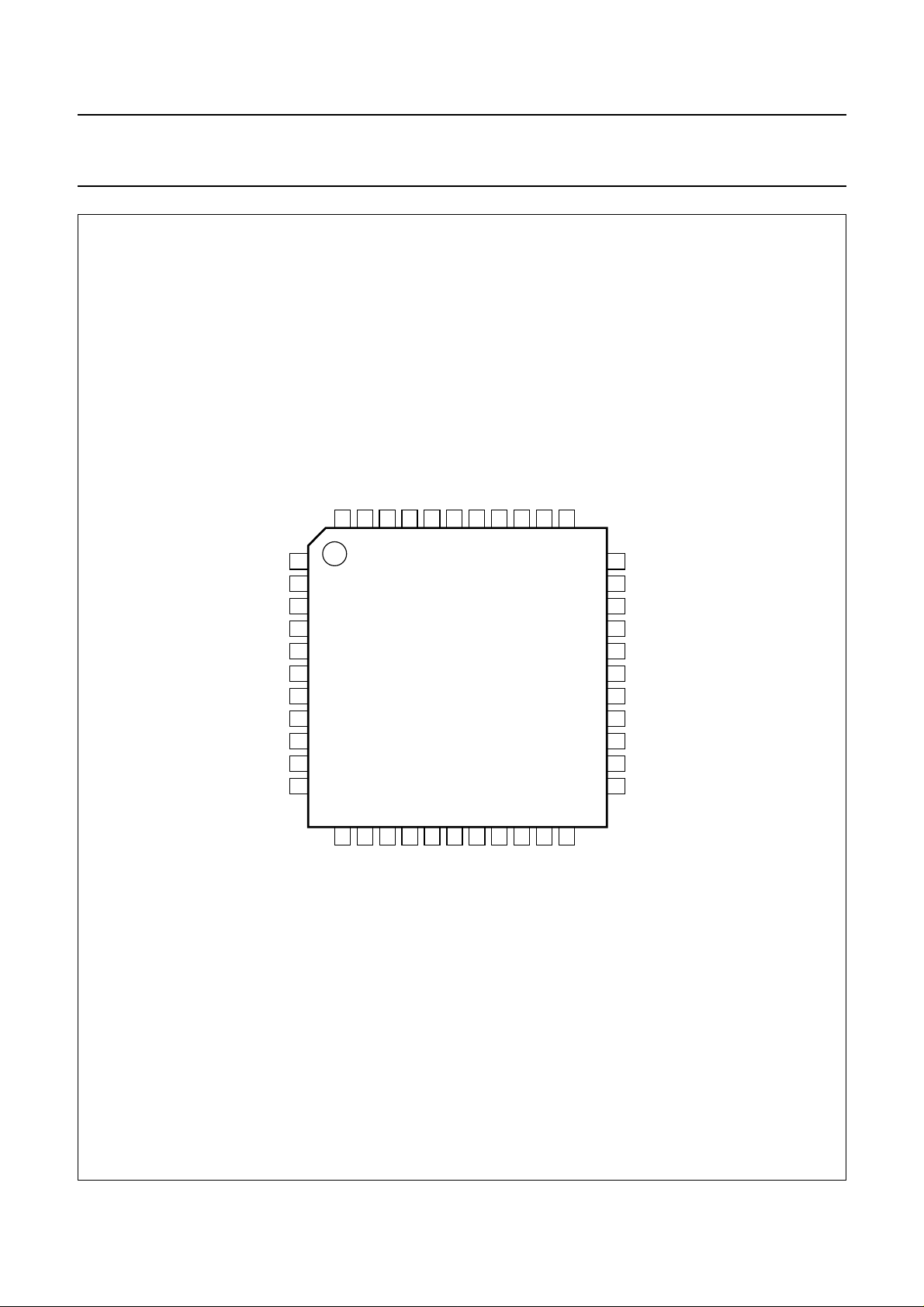
5 ORDERING INFORMATION
TYPE
NUMBER
NAME DESCRIPTION VERSION
PACKAGE
UDA1351H QFP44 plastic quad flat package; 44 leads (lead length 1.3 mm);
body 10 × 10 × 1.75 mm
6 BLOCK DIAGRAM
handbook, full pagewidth
V
DDA(DAC)
V
DDA(PLL)
V
SSA(PLL)
TEST1
V
DDD(C)
V
SSD(C)
L3MODE
L3CLOCK
L3DATA
SELSTATIC
SPDIF0
SPDIF1
SELCHAN
V
DDD
V
SSD
32
31
34
2
4
10
6
5
35
15
16
13
43
3
CLKOUT
CLOCK
AND
TIMING CIRCUIT
L3
INTERFACE
SLICER
11, 14,
28, 38,
40, 41
n.c.
29
IEC 958
DECODER
21
PREEM1
LOCK
30
42
PREEM0
TC
23
TEST2
39
DATA
OUTPUT
INTERFACE
33
BCKO
RTCB
UDA1351H
WSO
44
37
36
DATAO
V
SSA
DATAI
V
26
7
BCKI
VOUTL
DDA
27
AUDIO FEATURE PROCESSOR
8
9
SELCLK
WSI
18
DAC
NOISE SHAPER
INTERPOLATOR
19
SELSPDIF
V
SSA(DAC)
17
20
V
ref
VOUTR
25
24
DAC
DATA
INPUT
INTERFACE
22
SOT307-2
12
1
MGL976
MUTE
RESET
Fig.1 Block diagram.
2000 Feb 18 5

Philips Semiconductors Preliminary specification
96 kHz IEC 958 audio DAC UDA1351H
7 PINNING
SYMBOL PIN TYPE
(1)
DESCRIPTION
RESET 1 DISD reset input
V
DDD(C)
V
SSD
V
SSD(C)
2 DS digital supply voltage for core
3 DGND digital ground
4 DGND digital ground for core
L3DATA 5 DIOS L3 interface data input and output
L3CLOCK 6 DIS L3 interface clock input
DATAI 7 DISD I
BCKI 8 DISD I
WSI 9 DISD I
2
S-bus data input
2
S-bus bit clock input
2
S-bus word select input
L3MODE 10 DIS L3 interface mode input
n.c. 11 − not connected
MUTE 12 DID mute control input
SELCHAN 13 DID IEC 958 channel selection input
n.c. 14 − not connected
SPDIF0 15 AI IEC 958 channel 0 input
SPDIF1 16 AI IEC 958 channel 1 input
V
DDA(DAC)
17 AS analog supply voltage for DAC
VOUTL 18 AO DAC left channel analog output
SELCLK 19 DID clock source for PLL selection input
SELSPDIF 20 DIU IEC 958 data selection input
LOCK 21 DO SPDIF and PLL lock indicator output
VOUTR 22 AO DAC right channel analog output
TC 23 DID test pin; must be connected to digital ground (V
V
ref
V
SSA(DAC)
V
SSA
V
DDA
24 A DAC reference voltage
25 AGND analog ground for DAC
26 AGND analog ground
27 AS analog supply voltage
SSD
)
n.c. 28 − not connected
CLKOUT 29 DO clock output (256f
)
s
PREEM1 30 DO IEC 958 input pre-emphasis output 1
V
SSA(PLL)
V
DDA(PLL)
BCKO 33 DO I
31 AGND analog ground for PLL
32 AS analog supply voltage for PLL
2
S-bus bit clock output
TEST1 34 DIU test pin 1: must be connected to digital supply voltage (V
SELSTATIC 35 DIU static pin control selection input
DATAO 36 DO I
WSO 37 DO I
2
S-bus data output
2
S-bus word select output
n.c. 38 − not connected
TEST2 39 DISD test pin 2; must be connected to digital ground (V
SSD
)
n.c. 40 − not connected
DDD
)
2000 Feb 18 6
Philips Semiconductors Preliminary specification
96 kHz IEC 958 audio DAC UDA1351H
SYMBOL PIN TYPE
(1)
DESCRIPTION
n.c. 41 − not connected
PREEM0 42 DO IEC 958 input pre-emphasis output 0
V
DDD
43 DS digital supply voltage
RTCB 44 DID test pin; must be connected to digital ground (V
Note
1. See Table 1.
Table 1 Pin type references
PIN TYPE DESCRIPTION
DS digital supply
DGND digital ground
AS analog supply
AGND analog ground
DI digital input
DIS digital Schmitt-triggered input
DID digital input with internal pull-down resistor
DISD digital Schmitt-triggered input with internal pull-down resistor
DIU digital input with internal pull-up resistor
DO digital output
DIO digital input and output
DIOS digital Schmitt-triggered input and output
A analog reference voltage
AI analog input
AO analog output
SSD
)
2000 Feb 18 7
Philips Semiconductors Preliminary specification
96 kHz IEC 958 audio DAC UDA1351H
handbook, full pagewidth
DDD
RTCB
44
V
43
PREEM0
n.c.
42
41
n.c.
40
n.c.
TEST2
39
38
WSO
37
DATAO
SELSTATIC
36
35
TEST1
34
RESET
V
DDD(C)
V
SSD
V
SSD(C)
L3DATA
L3CLOCK
DATAI
BCKI
WSI
L3MODE
n.c.
22
VOUTR
33
BCKO
V
32
V
31
30
PREEM1
CLKOUT
29
28
n.c.
V
27
V
26
V
25
24
V
TC
23
MGL977
DDA(PLL)
SSA(PLL)
DDA
SSA
SSA(DAC)
ref
1
2
3
4
5
6
7
8
9
10
11
12
13
MUTE
SELCHAN
14
n.c.
UDA1351H
15
16
SPDIF0
SPDIF1
17
18
VOUTL
DDA(DAC)
V
19
20
SELCLK
SELSPDIF
21
LOCK
Fig.2 Pin configuration.
2000 Feb 18 8
Philips Semiconductors Preliminary specification
96 kHz IEC 958 audio DAC UDA1351H
8 FUNCTIONAL DESCRIPTION
8.1 Operating modes
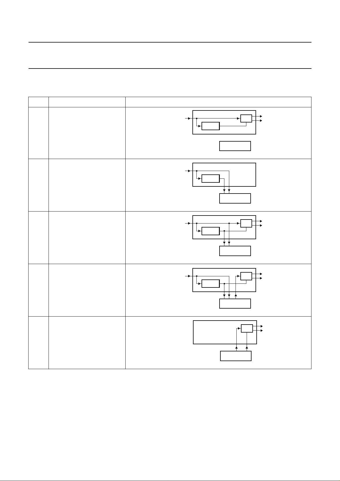
MODE DESCRIPTION SCHEMATIC
1 IEC 958 input to the DAC
input
IEC 958
DAC
CLOCK
2 IEC 958 input via the data
output interface to the DSP
3 IEC 958 input to the DAC and
via the data output interface to
the DSP
4 IEC 958 input via the data
output interface to the external
DSP and via the data input
interface to the DAC
input
IEC 958
input
IEC 958
input
IEC 958
CLOCK
CLOCK
CLOCK
DSP
DSP
DSP
DSP
MGS758
MGS759
DAC
MGS760
DAC
MGS761
5 Data input interface signal to
the DAC
DSP
DAC
MGS762
The UDA1351H is a low cost multi-purpose IEC 958 decoder DAC with a variety of operating modes.
In modes 1, 2, 3 and 4 the UDA1351H is clock master; it generates the clock for both the outgoing and incoming digital
data streams. Consequently, any device providing data for the UDA1351H via the data input interface in mode 4 will be
slave to the clock generated by the UDA1351H.
In mode 5 the UDA1351H locks to signal WSI from the digital data input interface. Conforming to IEC 958, the audio
sample frequency of the data input interface must be between 28.0 and 100.0 kHz.
2000 Feb 18 9

Philips Semiconductors Preliminary specification
96 kHz IEC 958 audio DAC UDA1351H
8.2 Clock regeneration and lock detection
The UDA1351H contains an on-board PLL for
regenerating a system clock from the IEC 958 input
bitstream or the incoming digital data stream via the data
input interface. In addition to the system clock for the
on-board digital sound processing the PLL also generates
a 256fsclock output for use in the application. In the
absence of an input signal the clock will generate a
minimum frequency to warrant system functionality.
Note: in case of no input signal, the PLL generates a
minimum frequency and the output spectrum shifts
accordingly. Since the analog output does not have a
analog mute, this means noise which is out of band noise
under normal operation conditions, can move into the
audio band.
When the on-board clock has locked to the incoming
frequency the lock indicator bit will be set and can be read
via the L3 interface. Internally the PLL lock indication is
combinedwith the PCM status bitof the input datastream.
When both the IEC 958 decoder and the on-board clock
have locked to the incoming signal and the input data
stream is PCM data, then pin LOCK will be asserted.
However, when the IC is locked but the PCM status bit
reports non-PCM data then pin LOCK is returned to LOW
level.
8.3 Mute
The UDA1351H is equipped with a cosine roll-off mute in
the DSP data path of the DAC part. Muting the DAC, by
pin MUTE (in static mode) or via bit MT (in L3 mode) will
result in a soft mute as presented in Fig.3. The cosine
roll-off soft mute takes 32 × 32 samples = 24 ms at a
sampling frequency of 44.1 kHz.
handbook, halfpage
1
mute
factor
0.8
0.6
0.4
0.2
0
01 3
2
MGS755
t (ms)
The lock indication output can be used, for example, for
muting purposes. The lock signal can be used to drive an
external analog muting circuit to prevent out of band noise
to become audible in case the PLL runs at its minimum
frequency (e.g. when there is no SPDIF input signal).
Fig.3 Mute as a function of raised cosine roll-off.
When operating in the L3 control mode the device will
mute on start-up. In L3 mode it is necessary to explicitly
switch off the mute for audio output bymeans of the MT bit
in the L3 register.
In the L3 mode pin MUTE does not have any function (the
same holds for several other pins) and can either be left
open-circuit (since it has an internal pull-down resistor) or
be connected to ground.
2000 Feb 18 10

Philips Semiconductors Preliminary specification
96 kHz IEC 958 audio DAC UDA1351H
8.4 Auto mute
By default the outputs of the digital data output interface
and the DAC will be muted until the IC is locked,
regardless the level on pin MUTE (in static mode) or the
state of bit MT of the sound feature register (in L3 mode).
In this way only valid data will be passed to the outputs.
This mute is done in the SPDIF interface and is a hard
mute, not a cosine roll-off mute.
If needed this muting can be bypassed by setting
bit AutoMTtologic 0viathe L3 interface. As a result the IC
will no longer mute during out-of-lock situations.
8.5 Data path
The UDA1351H data path consists of the slicer and the
IEC 958 decoder, the digital data output and input
interfaces, the audio feature processor, digital interpolator
and noise shaper and the digital-to-analog converters.
8.5.1 IEC 958 INPUT
The UDA1351H IEC 958 decoder can select 1 out of 2
IEC 958 input channels. An on-chip amplifier with
hysteresis amplifies the IEC 958 input signal to CMOS
level (see Fig.4).
The extracted key parameters are:
• Pre-emphasis
• Audio sample frequency
• Two-channel PCM indicator
• Clock accuracy.
Both the lock indicator and the key channel status bits are
accessible via the L3 interface.
The UDA1351H supports the following sample
frequencies and data bit rates:
• fs= 32.0 kHz, resulting in a data rate of 2.048 Mbits/s
• fs= 44.1 kHz, resulting in a data rate of 2.8224 Mbits/s
• fs= 48.0 kHz, resulting in a data rate of 3.072 Mbits/s
• fs= 64.0 kHz, resulting in a data rate of 4.096 Mbits/s
• fs= 88.2 kHz, resulting in a data rate of 5.6448 Mbits/s
• fs= 96.0 kHz, resulting in a data rate of 6.144 Mbits/s.
The UDA1351H supports timing level I, II and III as
specified by the IEC 958 standard.
handbook, halfpage
15,
16
UDA1351H
MGL975
75 Ω
10 nF
180 pF
SPDIF0,
SPDIF1
Fig.4 IEC 958 input circuit and typical application.
All 24 bits of data for left and right are extracted from the
input bitstream as well as several of the IEC 958 key
channel-status bits.
2000 Feb 18 11
 Loading...