

Philips UDA1350ATS Datasheet
INTEGRATED CIRCUITS
DATA SH EET
UDA1350ATS
IEC 60958 audio DAC
Product specification
Supersedes data of 2000 Mar 29
File under Integrated Circuits, IC01
2001 Mar 27

Philips Semiconductors Product specification
IEC 60958 audio DAC UDA1350ATS
CONTENTS
1 FEATURES
1.1 General
1.2 Control
1.3 IEC 60958 input
1.4 Digital sound processing and DAC
2 APPLICATIONS
3 GENERAL DESCRIPTION
4 QUICK REFERENCE DATA
5 ORDERING INFORMATION
6 BLOCK DIAGRAM
7 PINNING
8 FUNCTIONAL DESCRIPTION
8.1 Clock regeneration and lock detection
8.2 Mute
8.3 Auto mute
8.4 Data path
8.4.1 IEC 60958 input
8.4.2 Audio feature processor
8.4.3 Interpolator
8.4.4 Noise shaper
8.4.5 Filter stream DAC
8.5 Control
8.5.1 Static pin control mode
8.5.2 L3 control mode
8.6 L3 interface
8.6.1 General
8.6.2 Device addressing
8.6.3 Register addressing
8.6.4 Data write mode
8.6.5 Data read mode
8.6.6 Initialisation string
8.6.7 Overview of L3 interface registers
8.6.8 Writable registers
8.6.9 Readable registers
9 LIMITING VALUES
10 THERMAL CHARACTERISTICS
11 CHARACTERISTICS
12 TIMING CHARACTERISTICS
13 APPLICATION INFORMATION
14 PACKAGE OUTLINE
15 SOLDERING
15.1 Introduction to soldering surface mount
packages
15.2 Reflow soldering
15.3 Wave soldering
15.4 Manual soldering
15.5 Suitability of surface mount IC packages for
wave and reflow soldering methods
16 DATA SHEET STATUS
17 DEFINITIONS
18 DISCLAIMERS
2001 Mar 27 2

Philips Semiconductors Product specification
IEC 60958 audio DAC UDA1350ATS
1 FEATURES
1.1 General
• 2.7 to 3.6 V power supply
• Integrated digital filter and Digital-to-Analog Converter
(DAC)
• 256fssystem clock output
• 20-bit data path in interpolator
• High performance
• No analog post filtering required for DAC.
1.2 Control
2 APPLICATIONS
• Digital audio systems.
• Controlled either by means of static pins or via the
L3 microcontroller interface.
1.3 IEC 60958 input
• On-chip amplifier for converting IEC 60958 input to
CMOS levels
• Lock indication signal available on pin LOCK
• Lock indication signal combined on-chip with the Pulse
Code Modulation (PCM) status bit; in case non-PCM
has been detected pin LOCK indicates out-of-lock
• Key channel-status bits available via L3 interface (lock,
pre-emphasis, audio sample frequency, two channel
PCM indication and clock accuracy).
1.4 Digital sound processing and DAC
• Automatic de-emphasis when using IEC 60958 input
with 32.0, 44.1 and 48.0 kHz audio sample frequencies
• Soft muteby means of a cosine roll-off circuit selectable
via pin MUTE or the L3 interface
• dB linear volume control with 1 dB steps from 0 dB to
−60 dB and −∞ dB
• Bass boost and treble control in L3 control mode
• Interpolating filter (fsto 128fs) by means of a cascade of
a recursive filter and a FIR filter
• Third order noise shaper operating at 128fsgenerates
the bitstream for the DAC
• Filter stream digital-to-analog converter.
3 GENERAL DESCRIPTION
Available in two versions:
• UDA1350ATS:
– only IEC 60958 input to DAC in SSOP28 package.
• UDA1350AH:
– full featured version in QFP44 package.
The UDA1350ATS is a single chip IEC 60958 audio
decoder with an integrated stereo digital-to-analog
converter employing bitstream conversion techniques.
Alock indication signalis available onpin LOCK indicating
thatthe IEC 60958 decoderis locked. Thispinis also used
to indicate whetherPCM data is applied tothe input or not.
In the event non-PCM data has been detected, the device
indicates out-of-lock.
By default the DAC output and the data output interface
are muted when the decoder is out-of-lock. However, this
setting can be overruled in the L3 control mode.
2001 Mar 27 3
Philips Semiconductors Product specification
IEC 60958 audio DAC UDA1350ATS
4 QUICK REFERENCE DATA
SYMBOL PARAMETER CONDITIONS MIN. TYP. MAX. UNIT
Supplies
V
DDD
V
DDA
I
DDA(DAC)
I
DDA(PLL)
I
DDD
I
DDD(C)
P power consumption DAC in playback mode − 80 − mW
General
t
rst
T
amb
Digital-to-Analog Converter
V
o(rms)
(THD + N)/S total harmonic
S/N signal-to-noise ratio f
α
cs
∆V
o
digital supply voltage 2.7 3.0 3.6 V
analog supply voltage 2.7 3.0 3.6 V
analog supply current of DAC power-on − 8.0 − mA
power-down − 750 −µA
analog supply current of PLL − 0.7 − mA
digital supply current − 2.0 − mA
digital supply current of core − 16.0 − mA
DAC in Power-down mode − 58 − mW
reset active time − 250 −µs
ambient temperature −40 − +85 °C
output voltage (RMS value) note 1 − 900 − mV
f
= 1.0 kHz tone
i
distortion-plus-noise to signal
ratio
at 0 dB −−90 −85 dB
at −40 dB; A-weighted −−60 −55 dB
= 1.0 kHz tone;
i
95 100 − dB
code = 0; A-weighted
channel separation fi= 1.0 kHz tone − 96 − dB
unbalance of output voltages fi= 1.0 kHz tone − 0.1 0.4 dB
Note
1. The output voltage of the DAC is proportional to the DAC power supply voltage.
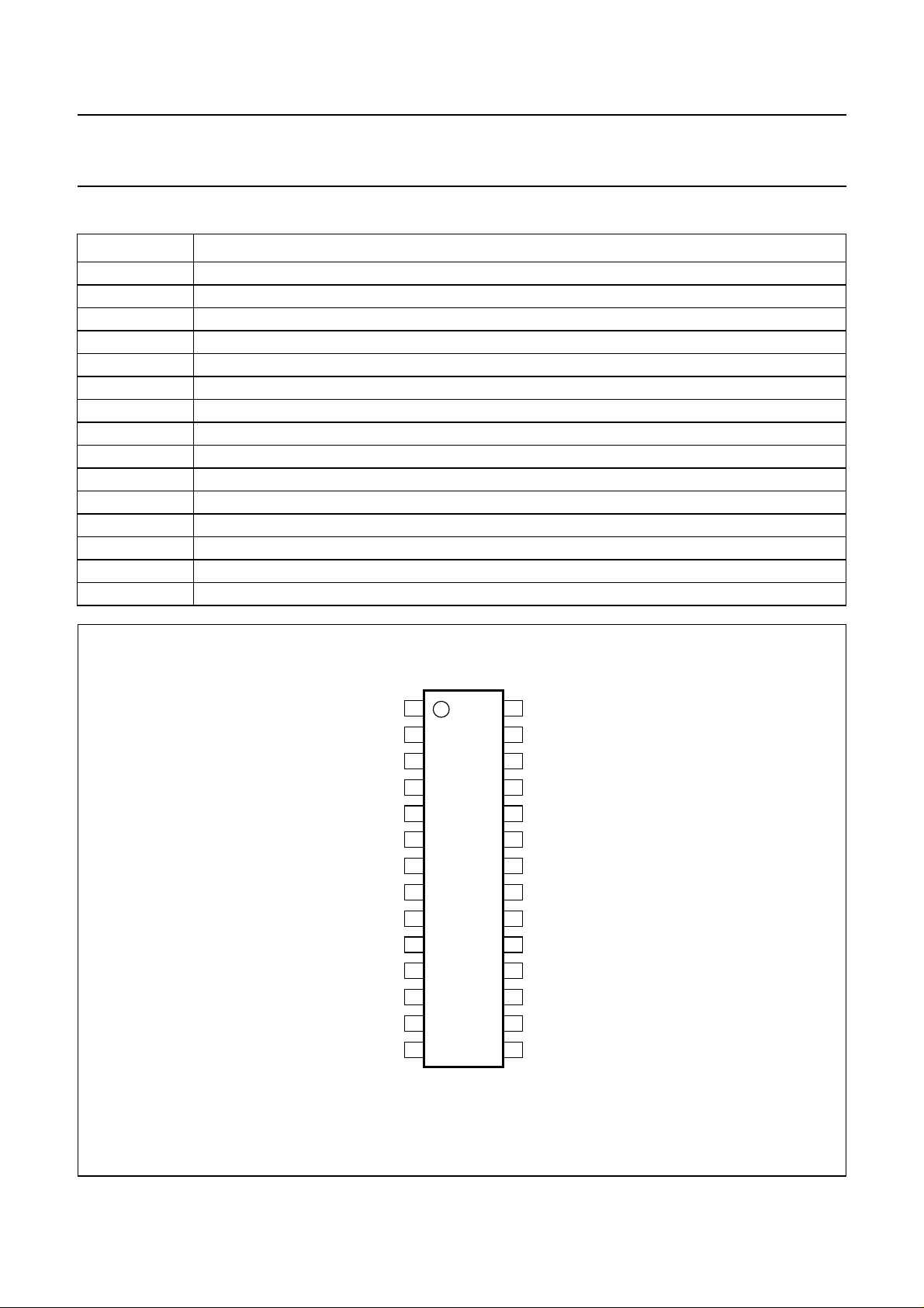
5 ORDERING INFORMATION
TYPE
NUMBER
NAME DESCRIPTION VERSION
PACKAGE
UDA1350ATS SSOP28 plastic shrink small outline package; 28 leads SOT341-1
2001 Mar 27 4
Philips Semiconductors Product specification
IEC 60958 audio DAC UDA1350ATS
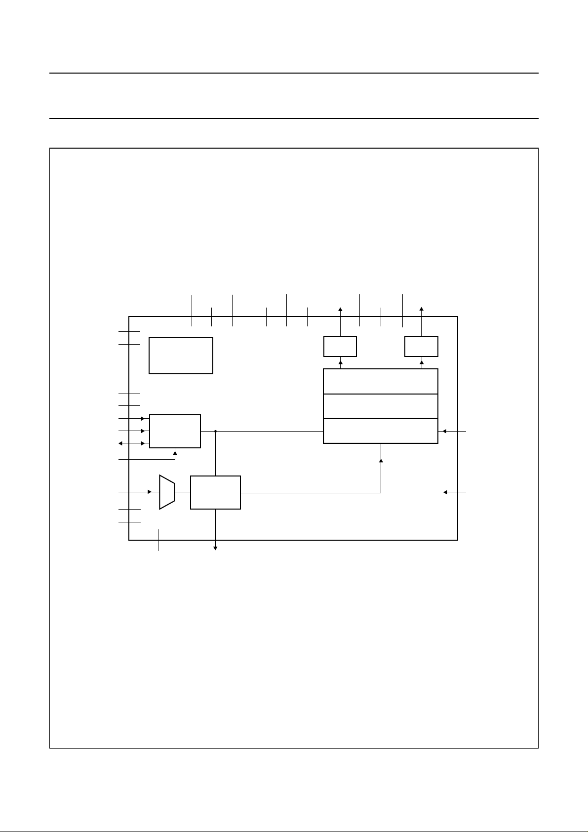
6 BLOCK DIAGRAM
handbook, full pagewidth
V
DDA(PLL)
V
SSA(PLL)
V
DDD(C)
V
SSD(C)
L3MODE
L3CLOCK
L3DATA
SELSTATIC
SPDIF
V
DDD
V
SSD
24
23
TIMING CIRCUIT
6
12
10
9
8
26
13
3
7
n.c.
TEST1 TEST3
CLOCK
AND
L3
INTERFACE
SLICER
1, 2, 27
TEST2
18
4
IEC 60958
DECODER
16
LOCK
TEST4
28
25
UDA1350ATS
V
SSA
V
DDA(DAC)
15
DAC
NOISE SHAPER
INTERPOLATOR
V
SSA(DAC)
14
V
DDA
VOUTL
21
22
AUDIO FEATURE PROCESSOR
V
ref
VOUTR
19
DAC
17
11
MUTE
5
RESET
MGL847
20
Fig.1 Block diagram.
2001 Mar 27 5
Philips Semiconductors Product specification
IEC 60958 audio DAC UDA1350ATS
7 PINNING
SYMBOL PIN TYPE
(1)
DESCRIPTION
n.c. 1 − not connected
n.c. 2 − not connected
V
DDD
TEST1 4 DID test pin 1; must be connected to digital ground (V
3 DS digital supply voltage
SSD
)
RESET 5 DISD reset input
V
DDD(C)
V
SSD
6 DS digital supply voltage for core
7 DGND digital ground
L3DATA 8 DIOS L3 interface data input and output
L3CLOCK 9 DIS L3 interface clock input
L3MODE 10 DIS L3 interface mode input
MUTE 11 DID mute control input
V
SSD(C)
12 DGND digital ground for core
SPDIF 13 AI IEC 60958 channel input
V
DDA(DAC)
14 AS analog supply voltage for DAC
VOUTL 15 AO analog DAC left channel output
LOCK 16 DO SPDIF and PLL lock indicator output
VOUTR 17 AO analog DAC right channel output
TEST2 18 DID test pin 2; must be connected to digital ground (V
V
ref
V
SSA(DAC)
V
SSA
V
DDA
V
SSA(PLL)
V
DDA(PLL)
19 A DAC reference voltage
20 AGND analog ground for DAC
21 AGND analog ground
22 AS analog supply voltage
23 AGND analog ground for PLL
24 AS analog supply voltage for PLL
SSD
)
TEST4 25 DIU test pin 4; must be connected to the digital supply voltage (V
SELSTATIC 26 DIU static pin control selection input
n.c. 27 − not connected
TEST3 28 DISD test pin 3; must be connected to digital ground (V
SSD
)
DDD
)
Note
1. See Table 1.
2001 Mar 27 6
Philips Semiconductors Product specification
IEC 60958 audio DAC UDA1350ATS
Table 1 Pin type references
PIN TYPE DESCRIPTION
DS digital supply
DGND digital ground
AS analog supply
AGND analog ground
DI digital input
DIS digital Schmitt-triggered input
DID digital input with internal pull-down resistor
DISD digital Schmitt-triggered input with internal pull-down resistor
DIU digital input with internal pull-up resistor
DO digital output
DIO digital input and output
DIOS digital Schmitt-triggered input and output
A analog reference voltage
AI analog input
AO analog output
handbook, halfpage
V
DDA(DAC)
n.c.
n.c.
V
DDD
TEST1
RESET
V
DDD(C)
V
SSD
L3DATA
L3CLOCK
L3MODE
MUTE
V
SSD(C)
SPDIF
1
2
3
4
5
6
7
UDA1350ATS
8
9
10
11
12
13
14
MGL845
TEST3
28
27
n.c.
26
SELSTATIC
25
TEST4
24
V
V
23
V
22
V
21
V
20
V
19
TEST2
18
VOUTR
17
LOCK
16
VOUTL
15
DDA(PLL)
SSA(PLL)
DDA
SSA
SSA(DAC)
ref
Fig.2 Pin configuration.
2001 Mar 27 7
Philips Semiconductors Product specification
IEC 60958 audio DAC UDA1350ATS
8 FUNCTIONAL DESCRIPTION
The UDA1350ATS is a low cost audio IEC 60958 decoder
withan on-board DAC.Theminimum audio inputsampling
frequency conforming to the IEC60958 standard is
28.0 kHz and the maximum audio sampling frequency is
54.0 kHz.
8.1 Clock regeneration and lock detection
The UDA1350ATS contains an on-board PLL for
regenerating a system clock from the IEC 60958 input
bitstream.
Note: If there is no input signal, the PLL generates a
minimum frequency and the output spectrum shifts
accordingly. Since the analog output does not have an
analog mute, this means noise that is out of band under
normal conditions can move into the audio band.
When the on-board clock has locked to the incoming
frequency, the lockindicator bit will be setand can be read
via the L3 interface. Internally, the PLL lock indication is
combined with thePCM status bit of theinput data stream.
Whenboth the IEC 60958decoder and theon-board clock
have locked to the incoming signal and the input data
stream is PCM data, pin LOCK will be asserted. However,
when the IC is locked but the PCM status bit reports
non-PCM data, pin LOCK is returned to LOW level.
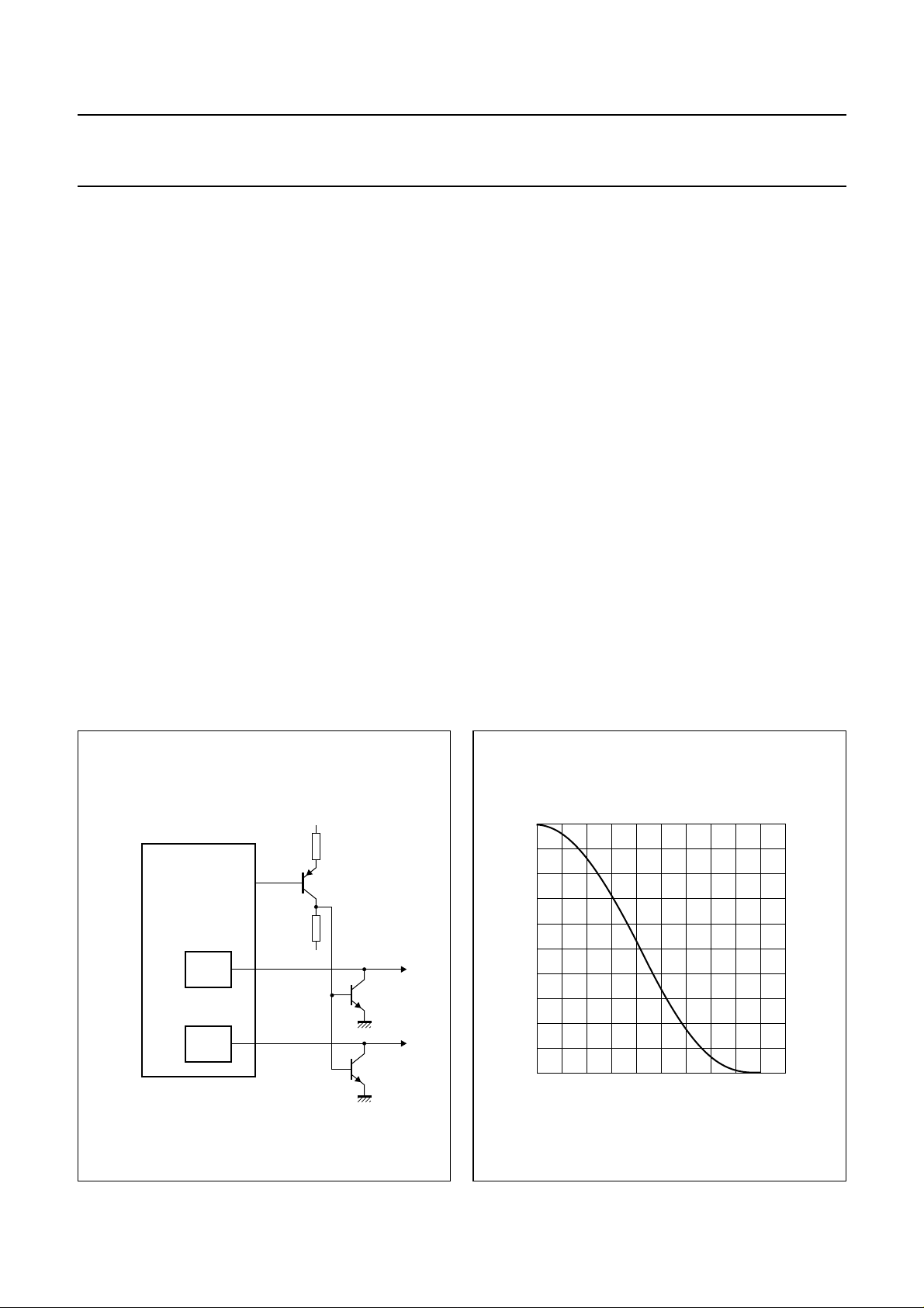
The lock indication output can be used, for example, for
muting purposes. The lock signal can be used to drive an
external analog muting circuit to preventout of band noise
from becoming audible when the PLL runs at its minimum
frequency (e.g. when there is no SPDIF input signal).
An example of the mute circuit is illustrated in Fig.3 where
VDD is the positive power supply and VSS is the negative
power supply.
8.2 Mute
The UDA1350ATS is equipped with a cosine roll-off mute
in the DSP data path of the DAC part. Muting the DAC, by
pin MUTE (in static mode) or via bit MT (in L3 mode) will
result in a soft mute as presented in Fig.4. The cosine
roll-off soft mute takes 32 × 32 samples = 24 ms at
44.1 kHz sampling frequency.
When operating in the L3 control mode the device will
mute on start-up. In L3 mode it is necessary to explicitly
switch off themute for audio output bymeans of the MT bit
in the L3 register.
In the L3 mode pin MUTE does not have any function (the
same holds for several other pins) and can either be left
open-circuit (since it has an internal pull-down resistor) or
be connected to ground.
LOCK
VOUTL
VOUTR
MGU352
V
DD
V
SS
handbook, halfpage
UDA1350ATS
DAC
LEFT
DAC
RIGHT
16
15
17
Fig.3 Example of external analog mute circuit.
2001 Mar 27 8
handbook, halfpage
1
mute
factor
0.8
0.6
0.4
0.2
0
01051525
MGU119
20
t (ms)
Fig.4 Mute as a function of raised cosine roll-off.
Philips Semiconductors Product specification
IEC 60958 audio DAC UDA1350ATS
8.3 Auto mute
By default the outputs of the digital data output interface
and the DAC will be muted until the IC is locked,
regardless the level on pin MUTE (in static mode) or the
state of bit MT of the sound feature register (in L3 mode).
In this way only valid data will be passed to the outputs.
This mute is done in the SPDIF interface and is a hard
mute, not a cosine roll-off mute.
If needed this muting can be bypassed by setting
bit AutoMTtologic 0 via the L3 interface.Asa result the IC
will no longer mute during out-of-lock situations.
8.4 Data path
The UDA1350ATS data path consists of the IEC 60958
decoder, the audio feature processor, digital interpolator
and noise shaper and the digital-to-analog converters.
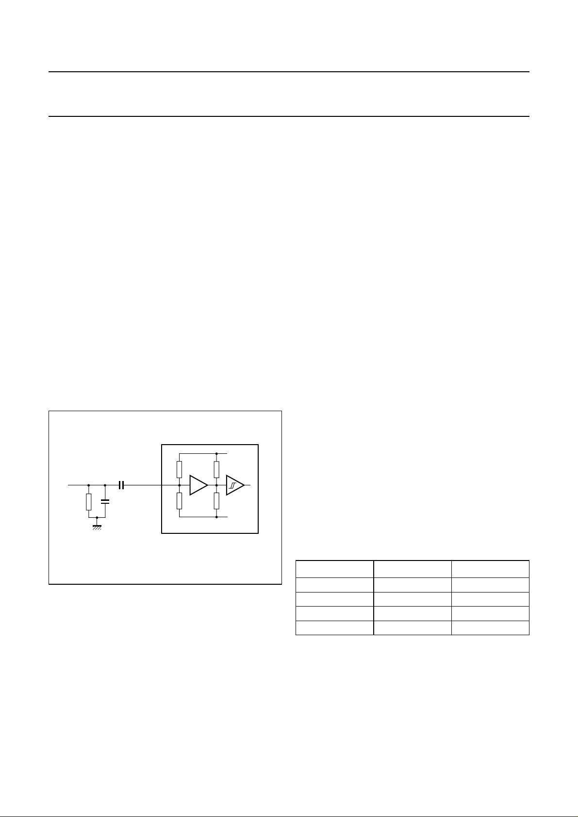
8.4.1 IEC 60958 INPUT
The UDA1350ATS IEC 60958 decoder features an
on-chip amplifier with hysteresis which amplifies the
IEC 60958 input signal to CMOS level (see Fig.5).
handbook, halfpage
75 Ω
10 nF
180 pF
13SPDIF
UDA1350ATS
MGS874
Fig.5 IEC 60958 input circuit and typical application.
All 24 bits of data for left and right are extracted from the
input bitstream as well as several of the IEC 60958 key
channel-status bits.
Both the lock indicator and the key channel status bits are
accessible via the L3 interface.
The UDA1350ATS supports the following sample
frequencies and data bit rates:
fs= 32.0 kHz, resulting in a data rate of 2.048 Mbits/s
fs= 44.1 kHz, resulting in a data rate of 2.8224 Mbits/s
fs= 48.0 kHz, resulting in a data rate of 3.072 Mbits/s.
The UDA1350ATS supports timing level I, II and III as
specified by the IEC 60958 standard.
8.4.2 AUDIO FEATURE PROCESSOR
The audio feature processor automatically provides
de-emphasis for the IEC 60958 data stream in the static
pin control mode and default mute at start-up in the
L3 control mode.
Whenused in theL3 control mode itprovides the following
additional features:
• Volume control using 6 bits
• Bass boost control using 4 bits
• Treble control using 2 bits
• Mode selection of the sound processing bass boost and
treble filters: flat, minimum and maximum
• Soft mute control with raised cosine roll-off
• De-emphasis selection of the incoming data stream for
fs= 32.0, 44.1 and 48.0 kHz.
8.4.3 INTERPOLATOR
TheUDA1350ATS includes an on-boardinterpolatingfilter
which converts the incoming data streamfrom 1fsto 128f
by cascading a recursive filter and a FIR filter.
Table 2 Interpolator characteristics
PARAMETER CONDITIONS VALUE (dB)
Pass-band ripple 0 to 0.45f
Stop band >0.65f
Dynamic range 0 to 0.45f
s
s
s
±0.03
−50
115
DC gain −−3.5
s
The extracted key parameters are:
• Pre-emphasis
• Audio sample frequency
• Two-channel PCM indicator
• Clock accuracy.
2001 Mar 27 9
8.4.4 NOISE SHAPER
The third-order noise shaper operates at 128fs. It shifts
in-band quantization noise to frequencies well above the
audio band. This noise shaping technique enables high
signal-to-noise ratios to be achieved. The noise shaper
output is converted into an analog signal using a filter
stream digital-to-analog converter.
Philips Semiconductors Product specification
IEC 60958 audio DAC UDA1350ATS
8.4.5 FILTER STREAM DAC
The Filter Stream DAC (FSDAC) is a semi-digital
reconstruction filter that converts the 1-bit data stream of
the noise shaper to an analog output voltage. The filter
coefficients are implemented as current sources and are
summed at virtual ground of the output operational
amplifier. In this way very high signal-to-noise
performance and low clock jitter sensitivity is achieved. A
postfilter is not needed dueto the inherentfilter function of
the DAC. On-board amplifiers convert the FSDAC output
current to anoutput voltagesignal capable of driving a line
output.
The output voltage of the FSDAC is scaled proportionally
with the power supply voltage.
8.5 Control
The UDA1350ATS can be controlled by means of static
pins or via the L3 interface. For optimum use of the
features of the UDA1350ATS the L3 control mode is
recommended since only basic functions are available in
the static pin control mode.
It should be noted that the static pin control mode and
L3 control mode are mutual exclusive. In the static pin
control mode pins L3MODE and L3DATA are used to
select the format for the data output and input interface.
8.5.1 STATIC PIN CONTROL MODE
The default values for all non-pin controlled settings are
identical to the default values at start-up in the L3 control
mode.
Table 3 Pin description of static pin control mode
PIN NAME VALUE FUNCTION
Mode selection pin
26 SELSTATIC 1 select static pin control mode; must be connected to V
DDD
Input pins
5 RESET 0 normal operation
1 reset
8 L3DATA 0 must be connected to V
9 L3CLOCK 0 must be connected to V
10 L3MODE 0 must be connected to V
SSD
SSD
SSD
11 MUTE 0 normal operation
1 mute active
Status pins
16 LOCK 0 clock regeneration and IEC 60958 decoder out-of-lock or non-PCM data
detected
1 clock regeneration and IEC 60958 decoder locked and PCM data detected
Test pins
4 TEST1 0 must be connected to digital ground (V
18 TEST2 0 must be connected to digital ground (V
25 TEST4 1 must be connected to digital supply voltage (V
28 TEST3 0 must be connected to digital ground (V
SSD
SSD
SSD
)
)
)
DDD
)
2001 Mar 27 10
 Loading...