

Philips UDA1345TS Datasheet
INTEGRATED CIRCUITS
DATA SH EET
UDA1345TS
Economy audio CODEC
Product specification
Supersedes data of 2000 Apr 18
File under Integrated Circuits, IC01
2000 Dec 19

Philips Semiconductors Productspecification
Economy audio CODEC UDA1345TS
CONTENTS
1 FEATURES
1.1 General
1.2 Multiple format input interface
1.3 DAC digital sound processing
1.4 Advanced audio configuration
2 GENERAL DESCRIPTION
3 ORDERING INFORMATION
4 QUICK REFERENCE DATA
5 BLOCK DIAGRAM
6 PINNING
7 FUNCTIONAL DESCRIPTION
7.1 Analog-to-Digital Converter (ADC)
7.2 Analog front-end
7.3 Decimation filter (ADC)
7.4 Interpolation filter (DAC)
7.5 Double speed
7.6 Noise shaper (DAC)
7.7 The Filter Stream DAC (FSDAC)
7.8 Power control
7.9 L3MODE or static pin control
7.10 L3 microcontroller mode
7.10.1 Pinning definition
7.10.2 System clock
7.10.3 Multiple format input/output interface
7.10.4 ADC input voltage control
7.10.5 Overload detection (ADC)
7.10.6 DC cancellation filter (ADC)
7.11 Static pin mode
7.11.1 Pinning definition
7.11.2 System clock
7.11.3 Mute and de-emphasis
7.11.4 Multiple format input/output interface
7.11.5 ADC input voltage control
7.12 L3 interface
7.12.1 Address mode
7.12.2 Data transfer mode
8 LIMITING VALUES
9 THERMAL CHARACTERISTICS
10 DC CHARACTERISTICS
11 AC CHARACTERISTICS (ANALOG)
12 AC CHARACTERISTICS (DIGITAL)
13 APPLICATION INFORMATION
14 PACKAGE OUTLINE
15 SOLDERING
15.1 Introduction to soldering surface mount
packages
15.2 Reflow soldering
15.3 Wave soldering
15.4 Manual soldering
15.5 Suitability of surface mount IC packages for
wave and reflow soldering methods
16 DATA SHEET STATUS
17 DEFINITIONS
18 DISCLAIMERS
2000 Dec 19 2

Philips Semiconductors Productspecification
Economy audio CODEC UDA1345TS
1 FEATURES
1.1 General
• Low power consumption
• 2.4 to 3.6 V power supply range with 3.0 V typical
• 5 V tolerant TTL compatible digital inputs
• 256, 384 and 512fs system clock
• Supports sampling frequencies from 8 to 100 kHz
• Non-inverting ADC plus integrated high-pass filter to
cancel DC offset
• The ADC supports 2 V (RMS) input signals
• Overload detector for easy record level control
• Separate power control for ADC and DAC
• Integrated digital interpolation filter plus non-inverting
DAC
• Functions controllable either by L3 microcontroller
interface or via static pins
• The UDA1345TSis pinand function compatible withthe
UDA1344TS
• Small package size (SSOP28).
1.2 Multiple format input interface
• I2S-bus, MSB-justified up to 24 bits and LSB-justified
16, 18 and 20 bits format compatible
• Three combined data formatswith MSB data output and
LSB 16, 18 and 20 bits data input
• 1fs input and output format data rate.
1.3 DAC digital sound processing
The sound processing features of the UDA1345TS can
only be used in L3 microcontroller mode:
• Digital dB-linear volume control (low microcontroller
load) via L3 microcontroller with 1 dB steps
• Digital de-emphasis for 32, 44.1 and 48 kHz
• Soft mute via cosine roll-off (in 1024 samples).
1.4 Advanced audio configuration
• Stereo single-ended input configuration
• Stereo line output (under microcontroller volume
control), no post filter required
• High linearity, dynamic range and low distortion.
2 GENERAL DESCRIPTION
The UDA1345TS is a single-chip stereo Analog-to-Digital
Converter (ADC) and Digital-to-Analog Converter (DAC)
with signal processing features employing bitstream
conversion techniques. The low power consumption and
low voltage requirements make the device eminently
suitable for use in low-voltage low-power portable digital
audio equipment which incorporates recording and
playback functions.
The UDA1345TS supports the I2S-bus data format with
word lengths of upto 24 bits, theMSB justified dataformat
with word lengths of up to 20 bits and the LSB justified
serial data format with word lengths of 16, 18 and 20 bits.
The UDA1345TS also supports three combined data
formats with MSB justified data output and LSB 16, 18
and 20 bits data input.
The UDA1345TS can be used either with static pin control
or under L3 microcontroller interface. In L3 mode the
UDA1345TS has basic sound features in playback mode
such as de-emphasis, volume control and soft mute.
Note: in contrast to the UDA1344TS, the UDA1345TS
does not have bass-boost and treble.
3 ORDERING INFORMATION
TYPE NUMBER
NAME DESCRIPTION VERSION
UDA1345TS SSOP28 plastic shrink small outline package; 28 leads; body width 5.3 mm SOT341-1
2000 Dec 19 3
PACKAGE
Philips Semiconductors Productspecification
Economy audio CODEC UDA1345TS
4 QUICK REFERENCE DATA
SYMBOL PARAMETER CONDITIONS MIN. TYP. MAX. UNIT
Supplies
V
DDA(ADC)
V
DDA(DAC)
V
DDD
I
DDA(ADC)
I
DDA(DAC)
I
DDO(DAC)
I
DDD
T
amb
Analog-to-digital converter
V
i(rms)
(THD + N)/S total harmonic distortion-plus-noise to
S/N signal-to-noise ratio V
α
cs
Digital-to-analog converter
V
o(rms)
(THD + N)/S total harmonic distortion plus
α
cs
S/N signal-to-noise ratio code = 0; A-weighted
ADC analog supply voltage 2.4 3.0 3.6 V
DAC analog supply voltage 2.4 3.0 3.6 V
digital supply voltage 2.4 3.0 3.6 V
ADC analog supply current operating mode − 10 14 mA
ADC power-down − 600 800 mA
ADC power-down all − 300 800 mA
DAC analog supply current operating mode − 4 7.0 mA
DAC power-down − 50 150 µA
DAC operational amplifier supply current operating mode − 2.0 3.0 mA
DAC power-down − 200 400 µA
digital supply current operating mode − 58mA
ADC and DAC power-down − 350 500 µA
ambient temperature −40 − +85 °C
input voltage (RMS value) notes 1 and 2 − 1.0 − V
at 0 dB
signal ratio
= 44.1 kHz −−85 −80 dB
f
s
f
=96kHz −−80 −75 dB
s
at −60 dB; A-weighted
fs= 44.1 kHz −−36 −30 dB
=96kHz −−34 −30 dB
f
s
= 0 V; A-weighted
i
f
= 44.1 kHz 90 96 − dB
s
= 96 kHz 90 94 − dB
f
s
channel separation − 100 − dB
output voltage (RMS value) note 3 − 900 − mV
at 0 dB
noise-to-signal ratio
fs= 44.1 kHz −−85 −80 dB
=96kHz −−80 −71 dB
f
s
at −60 dB; A-weighted
= 44.1 kHz −−37 −30 dB
f
s
=96kHz −−35 −30 dB
f
s
channel separation − 100 − dB
= 44.1 kHz 90 100 − dB
f
s
f
= 96 kHz 90 98 − dB
s
2000 Dec 19 4

Philips Semiconductors Productspecification
Economy audio CODEC UDA1345TS
SYMBOL PARAMETER CONDITIONS MIN. TYP. MAX. UNIT
Power performance
P
ADDA
P
DA
P
AD
P
PD
Notes
1. The input voltage can be up to 2 V (RMS) when the current through the ADC input pin is limited to approximately
1 mA by using a series resistor.
2. The input voltage to the ADC scales proportionally with the power supply voltage.
3. The output voltage of the DAC scales proportionally with the power supply voltage.
powerconsumption in recordand playback
− 64 − mW
mode
power consumption in playback only mode − 36 − mW
power consumption in record only mode − 46 − mW
power consumption in Power-down mode − 2.2 − mW
2000 Dec 19 5
Philips Semiconductors Productspecification
Economy audio CODEC UDA1345TS
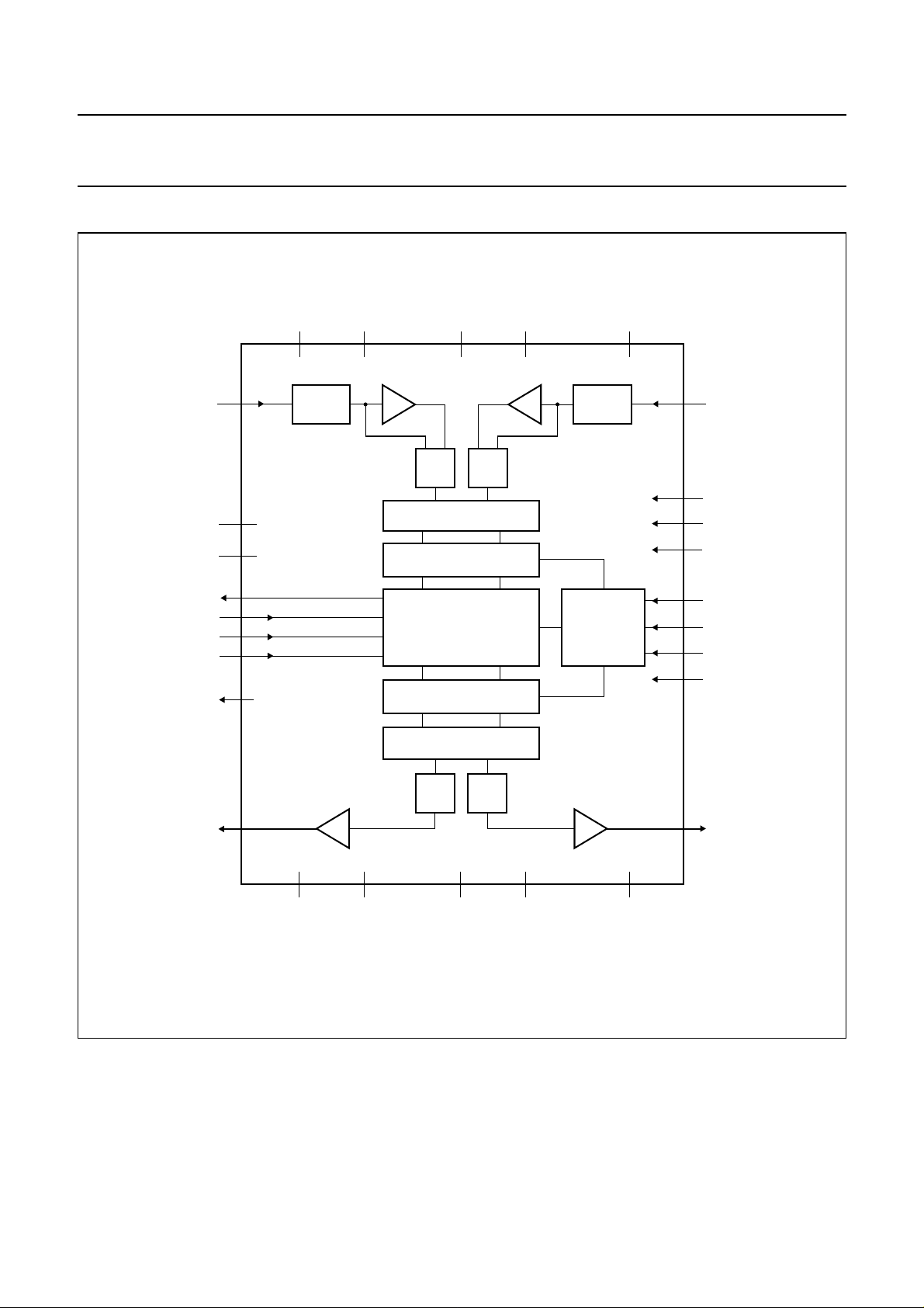
5 BLOCK DIAGRAM
handbook, full pagewidth
VINL
V
DDD
V
SSD
DATAO
BCK
WS
DATAI
MP1
V
DDA(ADC)VSSA(ADC)
21
3 5
10
11
18
16
17
19
9
0 dB/6 dB
SWITCH
DC-CANCELLATION FILTER
V
ADCP
ADC
DECIMATION FILTER
DIGITAL INTERFACE
INTERPOLATION FILTER
V
76 4
ADC
ADCN
V
ref(A)
0 dB/6 dB
SWITCH
L3-BUS
INTERFACE
21
20
13
14
15
12
UDA1345TS
NOISE SHAPER
VINR
8
MC1
MC2
MP5
MP2
MP3
MP4
SYSCLK
DAC
VOUTL
26
25 27 23 22
V
DDO
V
SSO
V
DDA(DAC)VSSA(DAC)
Fig.1 Block diagram.
2000 Dec 19 6
DAC
V
ref(D)
24
VOUTR
28
MGS875
Philips Semiconductors Productspecification
Economy audio CODEC UDA1345TS
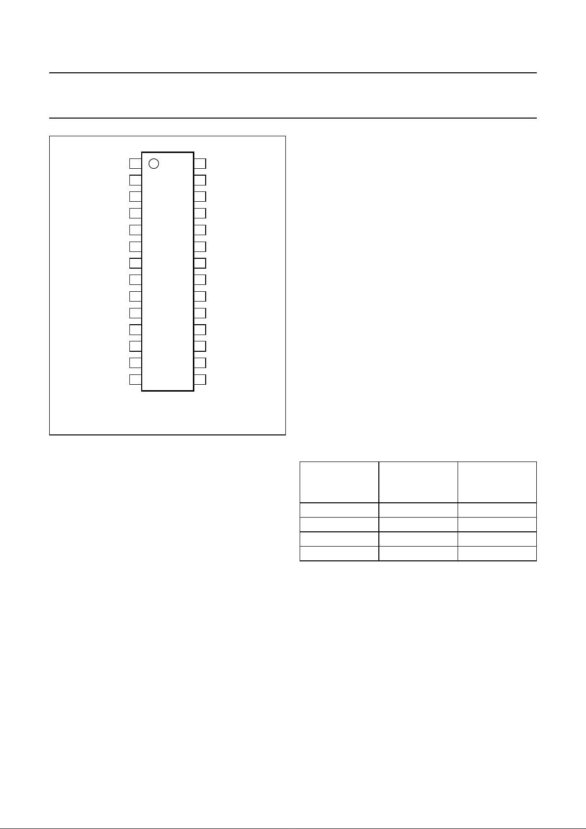
6 PINNING
SYMBOL PIN TYPE DESCRIPTION
V
SSA(ADC)
V
DDA(ADC)
VINL 3 analog input pad ADC input left
V
ref(A)
VINR 5 analog input pad ADC input right
V
ADCN
V
ADCP
MC1 8 5 V tolerant digital input pad with internal pull-down pad mode control 1 (pull-down)
MP1 9 5V tolerant slew rate controlled digital output pad multi purpose pin 1
V
DDD
V
SSD
SYSCLK 12 5 V tolerant digital Schmitt triggered input pad system clock 256, 384 or 512f
MP2 13 3-level input pad multi purpose pin 2
MP3 14 5 V tolerant digital Schmitt triggered input pad multi purpose pin 3
MP4 15 3-level input pad multi purpose pin 4
BCK 16 5 V tolerant digital Schmitt triggered input pad bit clock input
WS 17 5 V tolerant digital Schmitt triggered input pad word select input
DATAO 18 5 V tolerant slew rate controlled digital output pad data output
DATAI 19 5 V tolerant digital Schmitt triggered input pad data input
MP5 20 5 V tolerant digital Schmitt triggered input pad multi purpose pin 5 (pull down)
MC2 21 5 V tolerant digital input pad with internal pull-down pad mode control 2 (pull-down)
V
SSA(DAC)
V
DDA(DAC)
VOUTR 24 analog output pad DAC output right
V
DDO
VOUTL 26 analog output pad DAC output left
V
SSO
V
ref(D)
1 analog ground pad ADC analog ground
2 analog supply pad ADC analog supply voltage
4 analog pad ADC reference voltage
6 analog pad ADC negative reference voltage
7 analog pad ADC positive reference voltage
10 digital supply pad digital supply voltage
11 digital ground pad digital ground
s
22 analog ground pad DAC analog ground
23 analog supply pad DAC analog supply voltage
25 analog supply pad operational amplifier supply voltage
27 analog ground pad operational amplifier ground
28 analog pad DAC reference voltage
2000 Dec 19 7
Philips Semiconductors Productspecification
Economy audio CODEC UDA1345TS
7.1 Analog-to-Digital Converter (ADC)
handbook, halfpage
V
SSA(ADC)
V
DDA(ADC)
1
2
VINL
3
V
4
ref(A)
VINR
5
V
V
SYSCLK
ADCN
ADCP
MC1
MP1
V
DDD
V
SSD
MP2
MP3
6
7
UDA1345TS
8
9
10
11
12
13
Fig.2 Pin configuration.
MGS876
28
27
26
25
24
23
22
21
20
19
18
17
16
1514
V
ref(D)
V
SSO
VOUTL
V
DDO
VOUTR
V
DDA(DAC)
V
SSA(DAC)
MC2
MP5
DATAI
DATAO
WS
BCK
MP4
The stereo ADC of the UDA1345TS consists of two
5th-order Sigma-Delta modulators. They have a modified
Ritchie-coder architecture in a differential switched
capacitor implementation. The oversampling ratio is 64.
7.2 Analog front-end
The analog front-end isequipped with aselectable 0 dB or
6 dB gain block (the pin to select this mode is given in
Section 7.10). This block can be used in applications in
which both 1 V (RMS) and 2 V (RMS) input signals can be
input to the UDA1345TS.
In applications in which a 2 V (RMS) input signal is used,
a12kΩresistor must be used inseries with theinput ofthe
ADC.This forms a voltage divider together with the internal
ADC resistor and ensures that only 1 V (RMS) maximum
is input to the IC. Using this application for a 2 V (RMS)
input signal, the switch must be set to 0 dB. When a
1 V (RMS) input signal is input to the ADC in the same
application, the gain switch must be set to 6 dB.
An overview of the maximum input voltages allowed
againstthepresence of an external resistor andthe setting
of the gain switch is given in Table 1; the power supply
voltage is assumed to be 3 V.
7 FUNCTIONAL DESCRIPTION
The UDA1345TS accommodates slave mode only, this
means that in all applications the system devices must
provide the system clocks (being the system clock itself
and the digital audio interface signals).
Thesystem clock must be locked in frequency to the audio
digital interface input signals.
The BCK clock can be up to 128fs, or in other words the
BCK frequency is 128 times the Word Select (WS)
frequency or less: f
= < 128 × fWS.
BCK
Important: the WS edge MUST fall on the negative edge
oftheBCK at all times for properoperationof the digital I/O
data interface.
Note: the sampling frequency range is from 8 to 100 kHz,
however for the 512fs clock mode the sampling range is
from 8 to 55 kHz.
Table 1 Application modes using input gain stage
RESISTOR
(12 kΩ)
INPUT GAIN
SWITCH
MAXIMUM
INPUT
VOLTAGE
Present 0 dB 2 V (RMS)
Present 6 dB 1 V (RMS)
Absent 0 dB 1 V (RMS)
Absent 6 dB 0.5 V (RMS)
7.3 Decimation filter (ADC)
Thedecimationfrom 64fsto1fsis performed in two stages.
The first stage realizes a 4th-order characteristic.
sin x
----------- x
This filter decreases the sample rate by 8. The second
stage consists of 2 half-band filters and a recursive filter,
each decimating by a factor of 2.
2000 Dec 19 8

Philips Semiconductors Productspecification
Economy audio CODEC UDA1345TS
Table 2 Digital decimation filter characteristics
ITEM CONDITIONS VALUE (dB)
Pass-band ripple 0 − 0.45f
Stop band >0.55f
Dynamic range 0 − 0.45f
Overall gain when
DC −1.16
s
s
s
±0.05
−60
114
a 0 dB signal is
input to ADC to
digital output
Note:thedigitaloutputlevel is inversely proportional to the
ADC analog power supply. This means that with a
constant analog input level and increasing power supply
the digital output level will decrease proportionally.
7.4 Interpolation filter (DAC)
The digital filter interpolates from 1 to 128fsby means of a
cascade of a recursive filter and an FIR filter.
Table 3 Digital interpolation filter characteristics
ITEM CONDITIONS VALUE (dB)
Passband ripple 0 − 0.45f
Stopband >0.55f
s
Dynamic range 0 − 0.45f
s
s
±0.03
−65
116.5
Gain DC −3.5
7.7 The Filter Stream DAC (FSDAC)
The FSDAC is a semi-digital reconstruction filter that
converts the 1-bit data stream of the noise shaper to an
analog output voltage. The filter coefficients are
implemented as current sources and are summed at
virtual ground of the output operational amplifier. In this
way very high signal-to-noise performance and low clock
jitter sensitivity is achieved. A post filter is not needed due
to the inherent filter function of the DAC. On-board
amplifiers convert the FSDAC output current to an output
voltage signal capable of driving a line output.
The output voltage of the FSDAC is scaled proportionally
with the power supply voltage.
7.8 Power control
Intheeventthatthe DAC is powered-up or powered-down,
a cosine roll-off mute will be performed (when powering
down) or a cosine roll-up de-mute (when powering up) will
be performed. This is in order to prevent clicks when
powering up or down. This power-on/off mute takes
32 × 4 = 128 samples.
7.9 L3MODE or static pin control
The UDA1345TS can be used under L3 microcontroller
interface mode or under static pin control. The mode can
be set via the Mode Control (MC) pins MC1 (pin 8) and
MC2 (pin 21). The function of these pins is given in
Table 4.
7.5 Double speed
SInce the device supports a sampling range of
8 to 100 kHz, the device can support double speed (e.g.
for 44.1 kHz and 48 kHz sampling frequency) by just
doubling the system speed. In double speed all features
are available.
7.6 Noise shaper (DAC)
The 3rd-order noise shaper operates at 128fs. It shifts
in-band quantization noise to frequencies well above the
audio band. This noise shaping technique enables high
signal-to-noise ratios to be achieved. The noise shaper
output is converted into an analog signal using a filter
stream digital-to-analog converter.
2000 Dec 19 9
Table 4 Mode Control pins MC1 and MC2
MODE MC2 MC1
L3MODE LOW LOW
Test modes LOW HIGH
HIGH LOW
Static pin mode HIGH HIGH
Important: in L3MODE the UDA1345TS is completely pin
and function compatible with the UDA1340M and the
UDA1344TS.
Note: the UDA1345TS does NOT supportbass-boost and
treble.
 Loading...