

Philips UDA1344TS-N2 Datasheet

DATA SH EET
Preliminary specification
Supersedes data of 2000 Jan 27
File under Integrated Circuits, IC01
2000 Feb 04
INTEGRATED CIRCUITS
UDA1344TS
Low-voltage low-power stereo
audio CODEC with DSP features
2000 Feb 04 2
Philips Semiconductors Preliminary specification
Low-voltage low-power stereo audio
CODEC with DSP features
UDA1344TS
FEATURES
General
• Low power consumption
• 3.0 V power supply
• System clock of 256fs, 384fsand 512f
s
• Supports sampling frequencies from 8 to 55 kHz
• Non-inverting ADC plus integrated high-pass filter to
cancel DC offset
• ADC supports 2 V (RMS) input signals
• Overload detector for easy record level control
• Separate power control for ADC and DAC
• Integrated digital interpolation filter plus non-inverting
DAC
• Functions controllable either via L3 microcontroller
interface or via static pins
• UDA1344TS is pin and function compatible with
UDA1340M
• Small package size (SSOP28)
• Easy application.
Multiple format input interface
• I2S-bus, MSB-justified or LSB-justified
16, 18 and 20 bits format compatible
• Three combined data formats withMSB-justified output
and LSB-justified 16, 18 and 20 bits input
• 1fsinput and output format data rate.
DAC digital sound processing
The sound processing features of the UDA1344TS can be
used in the L3 mode only:
• Digital tone control, bass boost and treble
• Digital dB-linear volume control (low microcontroller
load) via L3 microcontroller
• Digital de-emphasis for 32, 44.1 and 48 kHz
• Soft mute.
Advanced audio configuration
• Stereo single-ended input configuration
• Stereo line output (under microcontroller volume
control), no post filter required
• High linearity, dynamic range and low distortion.
GENERAL DESCRIPTION
The UDA1344TS is a single-chip stereo Analog-to-Digital
Converter (ADC) and Digital-to-Analog Converter (DAC)
with signal processing features employing bitstream
conversion techniques. The low power consumption and
low voltage requirements make the device eminently
suitable for use in low-voltage low-power portable digital
audio equipment which incorporates recording and
playback functions.
The UDA1344TS supports the I2S-bus data format with
wordlengths of up to 20 bits, the MSB-justified data format
with word lengths of up to 20 bits and the LSB-justified
data format with word lengths of 16, 18 and 20 bits. The
UDA1344TS also supports three combined data formats
with MSB-justified data output and LSB-justified
16, 18 and 20 bits data input.
The UDA1344TS can be controlled either via static pins or
via the L3 interface. In the L3 mode the UDA1344TS has
special Digital Sound Processing (DSP) features in
playback mode such as de-emphasis, volume control,
bass boost, treble and soft mute.
ORDERING INFORMATION
TYPE
NUMBER
PACKAGE
NAME DESCRIPTION VERSION
UDA1344TS SSOP28 plastic shrink small outline package; 28 leads; body width 5.3 mm SOT341-1
2000 Feb 04 3
Philips Semiconductors Preliminary specification
Low-voltage low-power stereo audio
CODEC with DSP features
UDA1344TS
QUICK REFERENCE DATA
Notes
1. The input voltage can be up to 2 V (RMS) when the current through the ADC input pin is limited to approximately
1 mA by using a series resistor.
2. The input voltage to the ADC is inversely proportional to the supply voltage.
3. The output voltage of the UDA1344TS differs from the output voltage of the UDA1340M.
4. The output of the DAC scales proportionally with the supply voltage.
SYMBOL PARAMETER CONDITIONS MIN. TYP. MAX. UNIT
Supplies
V
DDA(ADC)
ADC analog supply voltage 2.7 3.0 3.6 V
V
DDA(DAC)
DAC analog supply voltage 2.7 3.0 3.6 V
V
DDO
operational amplifier supply voltage 2.7 3.0 3.6 V
V
DDD
digital supply voltage 2.7 3.0 3.6 V
I
DDA(ADC)
ADC analog supply current operating − 9.0 11.0 mA
ADC power-down − 3.5 5.0 mA
I
DDA(DAC)
DAC analog supply current operating − 4.0 6.0 mA
DAC power-down − 25 75 µA
I
DDO
operational amplifier supply current operating − 4.0 6.0 mA
DAC power-down − 250 350 µA
I
DDD
digital supply current operating − 6.0 9.0 mA
DAC power-down − 2.5 4.0 mA
ADC power-down − 3.5 5.0 mA
T
amb
ambient temperature −40 − +85 °C
Analog-to-digital converter
V
i(rms)
input voltage (RMS value) notes 1 and 2 − 1.0 − V
(THD + N)/S total harmonic distortion-plus-noise to
signal ratio
at 0 dB −−85 −80 dB
at −60 dB; A-weighted −−35 −30 dB
S/N signal-to-noise ratio V
i
= 0 V; A-weighted − 95 − dB
α
cs
channel separation − 100 − dB
Digital-to-analog converter
V
o(rms)
output voltage (RMS value) notes 3 and 4 − 900 − mV
(THD + N)/S total harmonic distortion-plus-noise to
signal ratio
at 0 dB −−90 −85 dB
at −60 dB; A-weighted −−37 − dB
S/N signal-to-noise ratio code = 0; A-weighted − 100 − dB
α
cs
channel separation − 100 − dB
Power performance
P
ADDA
power consumption in record and
playback mode
− 69 − mW
P
DA
power consumption in playback mode − 42 − mW
P
AD
power consumption in record mode − 37.5 − mW
P
PD
power consumption in power-down mode − 17 − mW
2000 Feb 04 4
Philips Semiconductors Preliminary specification
Low-voltage low-power stereo audio
CODEC with DSP features
UDA1344TS
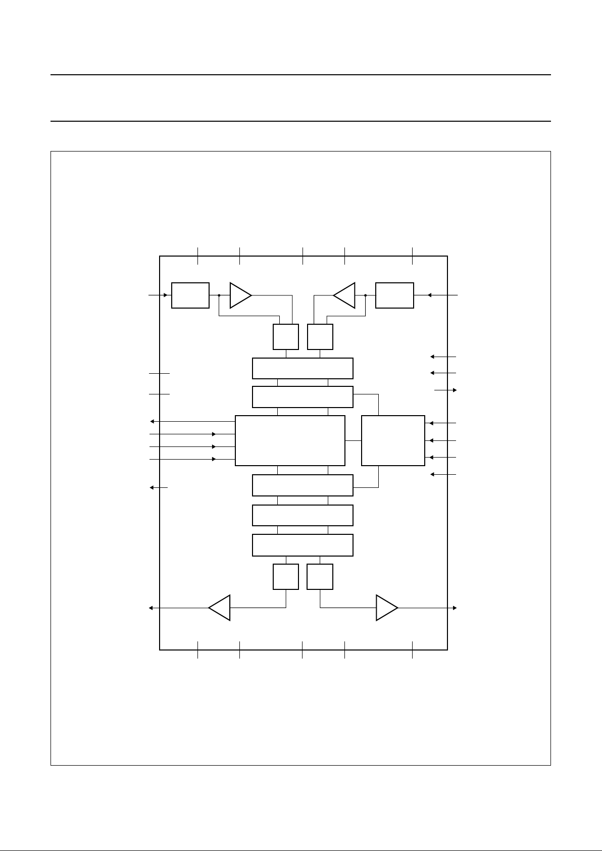
BLOCK DIAGRAM
Fig.1 Block diagram.
handbook, full pagewidth
MGL441
ADC
0 dB/6 dB
SWITCH
0 dB/6 dB
SWITCH
3
5
10
11
18
16
17
19
25 27 23 22
12
15
14
13
20
21
8
VINL
V
DDD
V
SSD
DATAO
BCK
WS
DATAI
MP1
VOUTL
28
24
9
26
VOUTR
SYSCLK
MP4
MP3
MP2
MP5
MC2
MC1
VINR
21
76 4
DECIMATION FILTER
DC-CANCELLATION FILTER
DIGITAL INTERFACE
L3-BUS
INTERFACE
ADC
DAC
V
ref(D)
V
DDO
V
SSO
DAC
INTERPOLATION FILTER
NOISE SHAPER
DSP FEATURES
V
DDA(ADC)VSSA(ADC)
V
ADCP
V
ADCN
V
ref(A)
UDA1344TS
V
DDA(DAC)VSSA(DAC)
2000 Feb 04 5
Philips Semiconductors Preliminary specification
Low-voltage low-power stereo audio
CODEC with DSP features
UDA1344TS
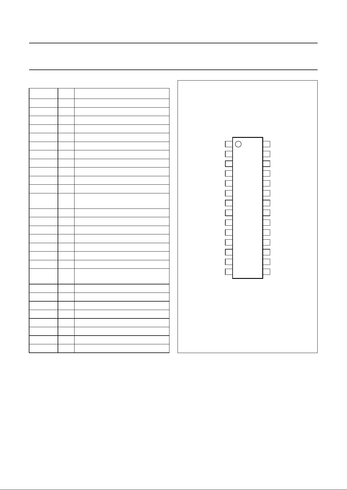
PINNING
SYMBOL PIN DESCRIPTION
V
SSA(ADC)
1 ADC analog ground
V
DDA(ADC)
2 ADC analog supply voltage
VINL 3 ADC input left
V
ref(A)
4 ADC reference voltage
VINR 5 ADC input right
V
ADCN
6 ADC negative reference voltage
V
ADCP
7 ADC positive reference voltage
MC1 8 mode control 1 input (pull-down)
MP1 9 multi purpose pin 1 output
V
DDD
10 digital supply voltage
V
SSD
11 digital ground
SYSCLK 12 system clock input:
256f
s
, 384fsor 512f
s
MP2 13 multi purpose pin 2 input
MP3 14 multi purpose pin 3 input
MP4 15 multi purpose pin 4 input
BCK 16 bit clock input
WS 17 word select input
DATAO 18 data output
DATAI 19 data input
MP5 20 multi purpose pin 5 output
(pull-down)
MC2 21 mode control 2 input (pull-down)
V
SSA(DAC)
22 DAC analog ground
V
DDA(DAC)
23 DAC analog supply voltage
VOUTR 24 DAC output right
V
DDO
25 operational amplifier supply voltage
VOUTL 26 DAC output left
V
SSO
27 operational amplifier ground
V
ref(D)
28 DAC reference voltage
Fig.2 Pin configuration.
handbook, halfpage
V
SSA(ADC)
V
DDA(ADC)
VINL
V
ref(A)
VINR
V
ADCN
V
ADCP
MC1
MP1
V
DDD
V
SSD
SYSCLK
MP2
MP3
V
ref(D)
V
SSO
VOUTL
V
DDO
V
DDA(DAC)
V
SSA(DAC)
VOUTR
MC2
MP5
DATAI
DATAO
WS
BCK
MP4
1
2
3
4
5
6
7
8
9
10
11
12
13
28
27
26
25
24
23
22
21
20
19
18
17
16
1514
UDA1344TS
MGL442
2000 Feb 04 6
Philips Semiconductors Preliminary specification
Low-voltage low-power stereo audio
CODEC with DSP features
UDA1344TS
FUNCTIONAL DESCRIPTION
The UDA1344TS accommodates slave mode only, this
means that in all applications the system devices must
provide the system clock. The system clock must be
locked in frequency to the digital interface input signals.
The BCK clock can be up to 128fs, or in other words the
BCK frequency is 128 times the Word Select (WS)
frequency or less: f
BCK
= < 128 × fWS.
Remarks:
1. The WS edge MUST fall on the negative edge of the
BCKclockatalltimesforproperoperationofthedigital
I/O data interface
2. The sampling frequency range is from 5 to 55 kHz
3. For MSB- and LSB-justified formats it is important to
have a WS signal with a duty factor of 50%.
Analog-to-Digital Converter (ADC)
The stereo ADC of the UDA1344TS consists of two
3rd-order Sigma-Delta modulators. They have a modified
Ritchie-coder architecture in a differential switched
capacitor implementation. The oversampling ratio is 128.
In contrast to the UDA1340M, the UDA1344TS supports
1 V (RMS) input signals and can be set, via an external
resistor, to support 2 V (RMS) input signals.
Analog front-end
The analog front-end is equippedwith a selectable 0 dBor
6 dB gain block. The pin to select the gain switch is given
in Section “L3 mode”. This block can be used in
applications in which both 1 V (RMS) and 2 V (RMS) input
signals are available.
In applications in which a 2 V (RMS) input signal is used,
a12kΩresistormust be connected in serieswith the input
of the ADC. This makes a voltage divider with the internal
ADC resistor and makes sure only 1 V (RMS) maximum is
inputto the IC. Using this application for a 2 V (RMS) input
signal, the gain switch must be set to 0 dB. When a
1 V (RMS) input signal is input to the ADC in the same
application, the gain switch must be set to 6 dB.
An overview of the maximum input voltages allowed
againstthepresenceofanexternalresistor and the setting
of the gain switch is given in Table 1.
Table 1 Application modes using input gain stage
Decimation filter (ADC)
The decimation from 128fsto 1fsis performed in 2 stages.
Thefirst stage realizes 3rd-order characteristic.This
filter decreases the sample rate by 16.
The second stage, a Finite Impulse Response (FIR) filter,
consists of 3 half-band filters, each decimating by a factor
of 2.
Table 2 Decimation filter characteristics
DC-cancellation filter (ADC)
AnoptionalInfiniteImpulse-Response(IIR)high-passfilter
is provided to remove unwanted DC components.
The operation is selected by the microcontroller via the
L3 interface. The filter characteristics are given in Table 3.
Table 3 DC-cancellation filter characteristics
RESISTOR
(12 kΩ)
INPUT GAIN
SWITCH
MAXIMUM
INPUT
VOLTAGE
Present 0 dB 2 V (RMS)
Present 6 dB 1 V (RMS)
Absent 0 dB 1 V (RMS)
Absent 6 dB 0.5 V (RMS)
ITEM CONDITIONS VALUE (dB)
Pass-band ripple 0 − 0.45f
s
±0.05
Stop band >0.55f
s
−60
Dynamic range 0 − 0.45f
s
108
Overall gain with
0 dB input to the
ADC
DC −1.16
ITEM CONDITIONS VALUE (dB)
Pass-band ripple − none
Pass-band gain − 0
Droop at 0.00045f
s
0.031
Attenuation at DC at 0.00000036f
s
>40
Dynamic range 0 − 0.45f
s
>110
sin x
x
----------- -
2000 Feb 04 7
Philips Semiconductors Preliminary specification
Low-voltage low-power stereo audio
CODEC with DSP features
UDA1344TS
Mute (ADC)
On recovery from power-down or switching on of the
system clock, the serial data output on pin DATAO is held
at LOW level until valid data is available from the
decimation filter. This time depends on whether the
DC-cancellation filter is selected:
• DC cancel off:
; t = 23.2 ms at f
s
= 44.1 kHz
• DC cancel on:
; t = 279 ms at f
s
= 44.1 kHz.
Interpolation filter (DAC)
The digital filter interpolates from 1f
s
to 128fsby means of
a cascade of a recursive filter and an FIR filter.
Table 4 Interpolation filter characteristics
Noise shaper (DAC)
The 3rd-order noise shaper operates at 128fs. It shifts
in-band quantization noise to frequencies well above the
audio band. This noise shaping technique enables high
signal-to-noise ratios to be achieved. The noise shaper
output is converted into an analog signal using a Filter
Stream Digital-to-Analog Converter (FSDAC).
Filter stream DAC
The FSDAC is a semi-digital reconstruction filter that
converts the 1-bit data stream of the noise shaper to an
analog output voltage. The filter coefficients are
implemented as current sources and are summed at
virtual ground of the output operational amplifier. In this
way very high signal-to-noise performance and low clock
jitter sensitivity is achieved. A post-filter is not needed due
to the inherent filter function of the DAC. On-board
amplifiers convert the FSDAC output current to an output
voltage signal capable of driving a line output.
The output voltage of the FSDAC scales proportionally
with the power supply voltage.
ITEM CONDITIONS VALUE (dB)
Pass-band ripple 0 − 0.45f
s
±0.03
Stop band >0.55f
s
−50
Dynamic range 0 − 0.45f
s
108
Gain DC −3.5
t
1024
f
s
------------ -
=
t
12288
f
s
----------------
=
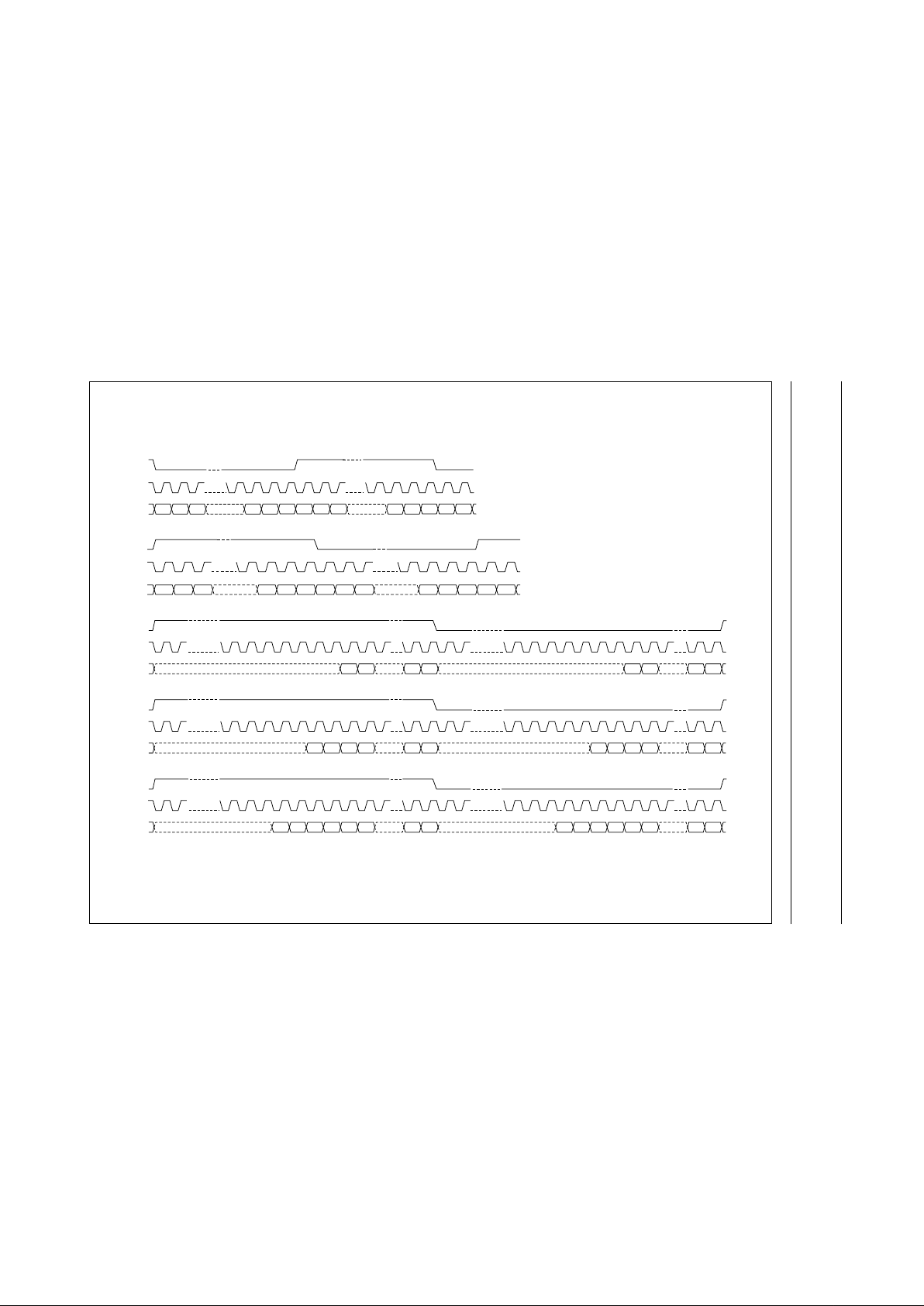
Multiple format input/output interface
The UDA1344TS supports the following data input/output
formats:
• I2S-bus format with data word length of up to 20 bits
• MSB-justifiedserialformatwithdatawordlength of up to
20 bits
• LSB-justified serial format with data word lengths of
16, 18 or 20 bits (in L3 mode only)
• Combined data formats:
– L3 mode: MSB-justified data output and
LSB-justified 16, 18 and 20 bits data input
– Static pin mode: MSB-justified data output and
LSB-justified 16 and 20 bits data input.
The formats are illustrated in Fig.3. Left and right
data-channel words are time multiplexed.
Control mode selection
The UDA1344TS can be used under L3 microcontroller
interface control or static pin control. The mode can be set
via the mode control pins MC1 and MC2 (see Table 5).
Table 5 Mode control pins
Important: in the L3 mode the UDA1344TS is completely
pin and function compatible with the UDA1340M.
PIN MC2 PIN MC1 MODE
LOW LOW L3 mode
LOW HIGH Test mode
HIGH LOW
HIGH HIGH Static pin mode
2000 Feb 04 8
Philips Semiconductors Preliminary specification
Low-voltage low-power stereo audio
CODEC with DSP features
UDA1344TS
This text is here in white to force landscape pages to be rotated correctly when browsing through the pdf in the Acrobat reader.This text is here in
_white to force landscape pages to be rotated correctly when browsing through the pdf in the Acrobat reader.This text is here inThis text is here in
white to force landscape pages to be rotated correctly when browsing through the pdf in the Acrobatreader. white to force landscapepages to be ...
d
book, full pagewidth
16
MSB B2 B3 B4 B5 B6
LEFT
LSB-JUSTIFIED FORMAT 20 BITS
WS
BCK
DATA
RIGHT
1518 1720 19 2 1
B19
LSB
16
MSB B2 B3 B4 B5 B6
1518 1720 19 2 1
B19 LSB
MSB MSBB2
21> = 812 3
LEFT
I
2
S-BUS FORMAT
WS
BCK
DATA
RIGHT
3
> = 8
MSB B2
MBL140
16
MSB
B2
LEFT
LSB-JUSTIFIED FORMAT 16 BITS
WS
BCK
DATA
RIGHT
15 2 1
B15
LSB
16
MSB B2
15 2 1
B15 LSB
16
MSB B2 B3 B4
LEFT
LSB-JUSTIFIED FORMAT 18 BITS
WS
BCK
DATA
RIGHT
1518 17 2 1
MSB B2 B3 B4
B17
LSB
16 1518 17 2 1
B17 LSB
MSB-JUSTIFIED FORMAT
WS
LEFT
RIGHT
321321
MSB B2 MSBLSB LSB MSB B2B2
> = 8 > = 8
BCK
DATA
Fig.3 Serial interface formats.
2000 Feb 04 9
Philips Semiconductors Preliminary specification
Low-voltage low-power stereo audio
CODEC with DSP features
UDA1344TS
Static pin mode
The UDA1344TS is set to static pin mode by setting both
pins MC1 and MC2 to HIGH level.
The controllable features in this mode are:
• System clock frequency selection
• Data input/output format selection
• De-emphasis and mute control
• Power-down and ADC input level selection.
PINNING DEFINITION
The pinning definition in the static pin mode is given in
Table 6.
Table 6 Pinning definition in static pin model
S
YSTEM CLOCK
In the static pin mode the options are 256fs and 384fs as
given in Table 7.
Table 7 System clock selection
M
UTE AND DE-EMPHASIS
The level definition of pin MP2 pin is given in Table 8.
Table 8 Levels for pin MP2
I
NPUT/OUTPUT DATA FORMAT SELECTION
The input/output data format can be selected using
pins MP1 and MP5 as given in Table 9.
Table 9 Data format selection
ADC INPUT VOLTAGE SELECTION AND POWER-DOWN
In the static pin mode the three-level pin MP4 is used to
select 0 or 6 dB gain and power-down.
Table 10 Levels for pin MP4
PIN DESCRIPTION
MP1 data input/output setting
MP2 three-level pin to select no
de-emphasis, de-emphasis or mute
MP3 256f
s
or 384fssystem clock selection
MP4 three-level pin to select
ADC power-down, ADC input
1 V (RMS) or ADC input 2 V (RMS)
MP5 data input/output setting
PIN MP3 SELECTION
LOW 256f
s
clock frequency
HIGH 384f
s
clock frequency
PIN MP2 SELECTION
LOW no de-emphasis and mute
0.5V
DDD
de-emphasis 44.1 kHz
HIGH mute
PIN MP1 PIN MP5 SELECTION
LOW LOW input: MSB-justified
LOW HIGH input: I
2
S-bus
HIGH LOW input: LSB-justified 20 bits;
output: MSB-justified
HIGH HIGH input: LSB-justified 16 bits;
output: MSB-justified
PIN MP4 SELECTION
LOW ADC power-down
0.5V
DDD
6 dB gain
HIGH 0 dB gain
 Loading...