

Philips UDA1343TT Datasheet
INTEGRATED CIRCUITS
DATA SH EET
UDA1343TT
Economy audio CODEC with
features
Product specification
Supersedes data of 2000 Jan 12
File under Integrated Circuits, IC01
2001 Jul 25
Philips Semiconductors Product specification
Economy audio CODEC with features UDA1343TT
FEATURES
General
• Low power consumption
• 2.4 to 3.6 V power supply range, with 3 V typical
• 5 V tolerant TTL compatible digital inputs
• 256, 384 and 512fs system clock
• Supports sampling frequencies from 8 to 110 kHz
• Non-inverting ADC plus integrated high-pass filter to
cancel DC offset
• The ADC supports 2 V (RMS) input signals
• Stereo PGA with 0 to 24 dB gain in 3 dB steps
• Overload detector for easy record level control
• Separate power control for ADC + PGA and DAC
• Integrated digital interpolation filter plus non-inverting
DAC
• Functions controllable by L3 microcontroller interface
• Small package size (TSSOP28)
• ADC and DAC output polarity can be set.
Multiple format input interface
• I2S-bus, MSB-justified up to 24 bits and LSB-justified
16, 18, 20 and 24 bits format compatible
• Four combined data formats with MSB data output and
LSB 16, 18, 20 and 24 bits data input
• 1fs input and output format data rate.
• High linearity, dynamic range and low distortion
• Digital silence detector
• Digital mixer for mixing ADC signal and playback signal
• ADC volume controlin 0.25 dB steps and cosine roll-off
mute.
APPLICATIONS
• Portable equipment which includes audio functions
• Digital video camera.
GENERAL DESCRIPTION
The UDA1343TT is a single-chip stereo Analog-to-Digital
Converter (ADC) and Digital-to-Analog Converter (DAC)
with basic signal processing features employing bitstream
conversion techniques. The low power consumption, the
small package size and low voltage requirements make
the device eminently suitable for use in low-voltage
low-power portable digital audio equipment which
incorporates recording and playback functions.
DAC digital sound processing
• Digital dB-linear volume control (low microcontroller
load) via L3 microcontroller in 0.25 dB steps
• Digital de-emphasis for 32, 44.1, 48 and 96 kHz
• Cosine roll-soft mute.
Advanced audio configuration
• Stereo single-ended input configuration
• Stereo line output (under microcontroller volume
control), no post filter required
ORDERING INFORMATION
TYPE
NUMBER
UDA1343TT TSSOP28 plastic thin shrink small outline package; 28 leads; body width 4.4 mm SOT361-1
2001 Jul 25 2
NAME DESCRIPTION VERSION
TheUDA1343TTis equipped with a digital mixer formixing
the ADC signal directly to the playback signal (forexample
for Karaoke applications). In the mixing mode the ADC
output signal can be output before or after the mixer.
The mixer can also be used as a selector to select
between the ADC or the digital data being played back at
the DAC.
PACKAGE
Philips Semiconductors Product specification
Economy audio CODEC with features UDA1343TT
QUICK REFERENCE DATA
SYMBOL PARAMETER CONDITIONS MIN. TYP. MAX. UNIT
Supplies
V
DDA(ADC)
V
DDA(DAC)
V
DDD
I
DDA(ADC)
I
DDA(DAC)
I
DDO(DAC)
I
DDD
T
amb
Analog-to-digital converter
V
i(rms)
(THD + N)/S totalharmonic distortion-plus-noise to
S/N signal-to-noise ratio V
α
cs
Digital-to-analog converter
V
o(rms)
(THD + N)/S totalharmonic distortion-plus-noise to
α
cs
S/N signal-to-noise ratio code = 0; A-weighted
ADC analog supply voltage 2.4 3.0 3.6 V
DAC analog supply voltage 2.4 3.0 3.6 V
digital supply voltage 2.4 3.0 3.6 V
ADC analog supply current operating mode − 10 − mA
ADC Power-down − 100 −µA
DAC analog supply current operating mode − 4 − mA
DAC Power-down − 50 −µA
DAC operational amplifier supply
current
operating mode − 2.5 − mA
DAC Power-down − 200 −µA
digital supply current operating mode − 5 − mA
ADC plus DAC
− 300 −µA
Power-down
ambient temperature −40 − +85 °C
input voltage (RMS value) notes 1, 2 and 3 − 1.0 − V
at 0 dB
signal ratio
f
= 44.1 kHz −−85 − dB
s
=96kHz −−81 − dB
f
s
at −60 dB; A-weighted
= 44.1 kHz −−37 − dB
f
s
=96kHz −−35 − dB
f
s
= 0 V; A-weighted
i
f
= 44.1 kHz − 97 − dB
s
=96kHz − 95 − dB
f
s
channel separation − 100 − dB
output voltage (RMS value) 860 900 940 mV
at 0 dB
signal ratio
= 44.1 kHz −−85 − dB
f
s
f
=96kHz −−80 − dB
s
at −60 dB; A-weighted
= 44.1 kHz −−37 − dB
f
s
f
=96kHz −−35 − dB
s
channel separation − 100 − dB
= 44.1 kHz − 100 − dB
f
s
f
=96kHz − 98 − dB
s
2001 Jul 25 3

Philips Semiconductors Product specification
Economy audio CODEC with features UDA1343TT
SYMBOL PARAMETER CONDITIONS MIN. TYP. MAX. UNIT
Power performance
P
ADDA
P
DA
P
AD
P
PD
Notes
1. The input voltage can be up to 2 V (RMS) when the current through the ADC input pin is limited to approximately
1 mA by using a series resistor.
2. The input voltage to the ADC scales proportionally with the power supply.
3. The performance figures and input voltage of the ADC are given with the PGA gain set to 0 dB.
power consumption in record and
− 64 − mW
playback mode
power consumption in playback mode − 36 − mW
power consumption in record mode − 46 − mW
power consumption in Power-down
− 2.0 − mW
mode
2001 Jul 25 4

Philips Semiconductors Product specification
Economy audio CODEC with features UDA1343TT
BLOCK DIAGRAM
handbook, full pagewidth
VINL
V
DDD
V
SSD
DATAO
BCK
WS
DATAI
OVERFL
V
DDA(ADC)VSSA(ADC)
21
3 5
PGA PGA
10
11
18
16
17
19
9
DIGITAL INTERFACE
DE-EMPHASIS/VOLUME/MUTE
UDA1343TT
V
ADCP
ADC
DECIMATION FILTER
DC/VOLUME/MUTE
DIGITAL MIXER
INTERPOLATION FILTER
NOISE SHAPER
V
76 4
ADC
ADCN
V
L3-BUS
INTERFACE
DIGITAL
SILENCE
DETECTOR
ref(A)
21
20
13
14
15
12
8
VINR
TEST1
TEST2
RESET
L3MODE
L3CLOCK
L3DATA
SYSCLK
DAC
VOUTL
26
25 27 23 22
V
DDO
V
SSO
V
DDA(DAC)VSSA(DAC)
Fig.1 Block diagram.
2001 Jul 25 5
DAC
V
ref(D)
24
VOUTR
28
MGL886

Philips Semiconductors Product specification
Economy audio CODEC with features UDA1343TT
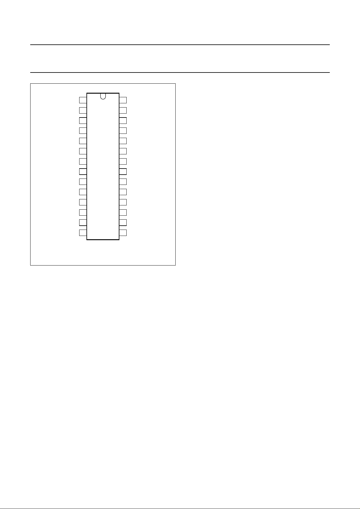
PINNING
SYMBOL PIN TYPE DESCRIPTION
V
SSA(ADC)
V
DDA(ADC)
VINL 3 analog input pad ADC input left
V
ref(A)
VINR 5 analog input pad ADC input right
V
ADCN
V
ADCP
TEST1 8 5 V tolerant digital input pad with internal pull-down pad test pin 1
OVERFL 9 5 V tolerant slew-rate controlled digital output pad ADC overload output
V
DDD
V
SSD
SYSCLK 12 5 V tolerant digital Schmitt triggered input pad system clock input 256, 384 or 512f
L3MODE 13 digital input pad L3MODE input
L3CLOCK 14 5 V tolerant digital Schmitt triggered input pad L3CLOCK input
L3DATA 15 5 V tolerant digital Schmitt triggered input with pull-down,
BCK 16 5 V tolerant digital Schmitt triggered input pad bit clock input
WS 17 5 V tolerant digital Schmitt triggered input pad word select input
DATAO 18 5 V tolerant slew-rate controlled digital output pad data output
DATAI 19 5 V tolerant digital Schmitt triggered input pad data input
RESET 20 5 V tolerant digital Schmitt triggered input pad with
TEST2 21 5 V tolerant digital input pad with internal pull-down pad test pin 2
V
SSA(DAC)
V
DDA(DAC)
VOUTR 24 analog output pad DAC output right
V
DDO
VOUTL 26 analog output pad DAC output left
V
SSO
V
ref(D)
1 analog ground pad ADC analog ground
2 analog supply pad ADC analog supply voltage
4 analog pad ADC reference voltage
6 analog pad ADC negative reference voltage
7 analog pad ADC positive reference voltage
10 digital supply pad digital supply voltage
11 digital ground pad digital ground
L3DATA input
slew rate controlled output pad
reset input
internal pull-down
22 analog ground pad DAC analog ground
23 analog supply pad DAC analog supply voltage
25 analog supply pad operational amplifier supply voltage
27 analog ground pad operational amplifier ground
28 analog pad DAC reference voltage
s
2001 Jul 25 6
Philips Semiconductors Product specification
Economy audio CODEC with features UDA1343TT
Reset
handbook, halfpage
V
SSA(ADC)
V
DDA(ADC)
L3CLOCK
1
2
VINL
3
V
4
ref(A)
VINR
5
V
V
OVERFL
SYSCLK
L3MODE
ADCN
ADCP
TEST1
V
DDD
V
SSD
6
7
UDA1343TT
8
9
10
11
12
13
Fig.2 Pin configuration.
MGL887
28
27
26
25
24
23
22
21
20
19
18
17
16
1514
V
ref(D)
V
SSO
VOUTL
V
DDO
VOUTR
V
DDA(DAC)
V
SSA(DAC)
TEST2
RESET
DATAI
DATAO
WS
BCK
L3DATA
Pin 20 is a reset pin (active HIGH), which resets the
internal digital core of the IC and also resets all feature
values of the L3 interface to their default settings as given
in Tables 8 and 9.
Since the RESET pin is a pull-down pad with
Schmitt-trigger, a Power-On Reset (POR) function can be
made by connecting this pinto the digital power supply via
a capacitor.
Note: care must be taken that during the HIGH period of
the reset signal it is best to have at least 8 SYSCLK clock
cycles to properly reset the device.
Analog-to-Digital Converter (ADC)
The stereo ADC of the UDA1343TT consists of two
5th-order Sigma-Delta modulators. They have a modified
Ritchie-coder architecture in a differential switched
capacitor implementation. The oversampling ratio is 64.
Analog front-end
The overall system gain is proportional to V
. The 0 dB
DDA
input level is defined as that which gives a −1dB
Full-Scale (FS) digital output (relative to the full-scale
swing).
FUNCTIONAL DESCRIPTION
The UDA1343TT accommodates slave mode only, this
means that in all applications the system devices must
provide the system clock and the serial audio clock
signals.
Thesystemclock must be locked infrequencytothe digital
interface input signals.
The BCK clock can be up to 128fs, or in other words the
BCK frequency f
frequency fWS or less: f
is 128 times the Word Select (WS)
BCK
= < 128 × fWS.
BCK
Important: the WS edge MUST fall on the negative edge
of the BCK at all times for correct operation of the digital
I/O data interface.
Note: the sampling frequency range is from 8 to 110 kHz,
however for the 512f
clock mode the sampling range is
s
from 8 to 55 kHz.
The analog front-end is equipped with a Programmable
Gain Amplifier (PGA) which can be controlled via the L3
interface. The control range is from 0 dB to 24 dB gain in
3 dB steps independant for left and right.
In applications in which a 2 V (RMS) input signal is used,
a12kΩresistormust be connectedin series withthe input
of the ADC. This makes a voltage divider with the internal
ADC resistor andmakes sure only 1 V (RMS) maximumis
input to the IC. Using this application for a2 V (RMS) input
signal, the switch must be set to 0 dB. When a 1 V (RMS)
inputsignal is input totheADC in the sameapplication,the
gain switch of the PGA must be set to 6 dB via the L3
interface.
An overview of the maximum input voltages allowed
againstthe presence of an externalresistorand the setting
of the gain switch is given in Table 1.
2001 Jul 25 7
Philips Semiconductors Product specification
Economy audio CODEC with features UDA1343TT
Table 1 Application modes using input gain stage
RESISTOR
(12 kΩ)
PGA GAIN
MAXIMUM
INPUT
VOLTAGE
Present 0 dB 2V (RMS)
Present 6 dB 1V (RMS)
Absent 0 dB 1V (RMS)
Absent 6 dB 0.5 V (RMS)
Decimation filter (ADC)
Thedecimation from 64fsto1fsisperformed in twostages.
The first stage realizes a 4th-order characteristic.
sin x
----------- x
This filter decreases the sample rate by 16. The second
stage consists of 2 half-band filters and a recursive filter,
each decimating by a factor of 2.
Table 2 Digital decimation filter characteristics
ITEM CONDITIONS VALUE (dB)
Pass-band ripple 0 − 0.45f
Stop band >0.55f
Dynamic range 0 − 0.45f
Overall gain with
DC −1.16
s
s
s
±0.05
−50
114
0 dB input to the
ADC
In the ADC path there is a volume control with a range of
0dBto−66 dB and −∞ dB in 0.25 dB steps, and a cosine
roll-off soft mute.
Table 3 Digital interpolation filter characteristics
ITEM CONDITIONS VALUE (dB)
Pass-band ripple 0 − 0.45f
Stop band >0.55f
Dynamic range 0 − 0.45f
s
s
s
±0.03
−65
116.5
Gain DC −3.5
Digital silence detector
The UDA1343 is equipped with a digital silence detector
on the digital data input. This detects whether a certain
amount of consecutive samples are 0. The status of the
digital silence detector can be read from the
microcontroller interface.
The number of samples can be set via the L3 interface to
3200, 4800, 9600 or 19600 samples.
The digital silence detection status can be read from the
microcontroller interface.
Mute
Muting the DAC will result in a cosine roll-off soft mute,
using32 × 4 = 128 samples (at 44.1 kHz thisis 3 ms). The
cosine roll-off curve is illustrated in Fig.3.
handbook, halfpage
1
mute
factor
0.8
MGS755
Note:thedigital output level is inversely proportional tothe
ADC analog power supply. This means that with a
constant analog input level and increasing analog power
supply, the digital output level will decrease proportionally.
Overload detection (ADC)
In practice the output is used to indicate whenever the
output data, ineither the left or rightchannel, is larger than
−1 dB (the actual figure is −1.16 dB) of the maximum
possible digital swing. When this condition is detected the
OVERFL output (pin 9) is forced HIGH for at least 512f
s
cycles (11.6 ms at fs= 44.1 kHz). This time-out is resetfor
each infringement.
Interpolation filter (DAC)
The digital filter interpolates from 1 to 128fsby means of a
cascade of a recursive filter and an FIR filter.
2001 Jul 25 8
0.6
0.4
0.2
0
01 3
2
t (ms)
Fig.3 Mute as a function of raised cosine roll-off.
Philips Semiconductors Product specification
Economy audio CODEC with features UDA1343TT
Double speed
SInce the device supports a sampling range of
8 to 110 kHz, the device can support double speed (e.g.
for 44.1 kHz and 48 kHz) by just doubling the system
speed. In double speed all features are available.
Digital mixer
The UDA1343TT has a digital mixer which can mix the
ADC signal to the playback signal. A functional block
diagram of the mixer mode is given in Fig.4.
When the device is in mixer mode, care is taken to avoid
clipping. This is done by reducing both signals by −6dB
before mixing. After mixing there is master volume and
mute, after which the signal is reamplified digitally by 6 dB.
handbook, full pagewidth
from ADC
and decimator
DIGITAL
DC FILTER
ADC volume + mute master volume + mute
VOLUME +
MUTE
−6 dB
The codec can be set to mixer mode via the L3 interface
by setting the MIX bit HIGH.
In the mixer mode there are 3 volume and mute controls
available; one for the ADC channel, one for the playback
channel and one for the master (equal sum) signal.
All three volume ranges can be controlled in 0.25 dB
steps.
In the mixer mode, the ADC volume control is used for
mixing purposes. The decimator output signal can be
output from the chip before the ADC volume control or
after the ADC volume control. This can be set via the L3
interface using the ADC output select bit.
+
VOLUME +
MUTE
+6 dB
to interpolator
and DAC
ADC_OUT
select (L3)
2
I
S-bus
output
−6 dB
VOLUME +
MUTE
I2S-bus
input
UDA1343TT
2
S-bus volume + mute
I
Fig.4 Mixing feature in the UDA1343TT.
MGL888
2001 Jul 25 9

Philips Semiconductors Product specification
Economy audio CODEC with features UDA1343TT
Digital output signal
The output to the digital output of the UDA1343TT can be
selected from 3 positions, using the two bits ADC_OUT
select in the L3 microcontroller interface. The 3 positions
are as follows:
• Directly from the ADC and decimator (default)
• After volume control and mute in the ADC data path
• After the digital mixer and before master volume control
and mute. It should be noted that this output is before
the +6 dB gain. This is done in order to prevent clipping
at the mixer output at all times.
Noise shaper (DAC)
The 3rd-order noise shaper operates at 128fs. It shifts
in-band quantization noise to frequencies well above the
audio band. This noise shaping technique enables high
signal-to-noise ratios to be achieved. The noise shaper
output is converted into an analog signal using a Filter
Stream Digital-to-Analog Converter (FSDAC).
The Filter Stream DAC (FSDAC)
The FSDAC is a semi-digital reconstruction filter that
converts the 1-bit data stream of the noise shaper to an
analog output voltage. The filter coefficients are
implemented as current sources and are summed at
virtual ground of the output operational amplifier.
In this way very high signal-to-noise performance and low
clock jitter sensitivity is achieved. A post-filter is not
needed due to the inherent filter function of the DAC.
On-board amplifiers convert the FSDAC output current to
an output voltage signal capable of driving a line output.
The output voltage of the FSDAC scales proportionally
with the power supply voltage.
Multiple format input/output audio interface
The digital audio interface supports multiple standards:
• I2S-bus with data word length of up to 24 bits
• MSB-justifiedserial format with data wordlengthof up to
24 bits
• LSB-justified data formats with word lengths of 16, 18,
20 and 24 bits
• Four combined data formats with MSB data output
and 16, 18, 20 and 24 LSB data input.
The digital audio interface formats are illustrated in Fig.5.
2001 Jul 25 10
This text is here in white to force landscape pages to be rotated correctly when browsing through the pdf in the Acrobat reader.This text is here in
d
_white to force landscape pages to be rotated correctly when browsing through the pdf in the Acrobat reader.This text is here inThis text is here in
white to force landscape pages to be rotated correctly when browsing through the pdf in the Acrobat reader. white to force landscape pages to be ...
2001 Jul 25 11
book, full pagewidth
Philips Semiconductors Product specification
Economy audio CODEC with features UDA1343TT
WS
BCK
DATA
WS
BCK
DATA
WS
BCK
DATA
WS
BCK
DATA
MSB B2
MSB B2 MSBLSB LSB MSB B2B2
LEFT
INPUT FORMAT I
LEFT
MSB-JUSTIFIED FORMAT
LEFT
LEFT
RIGHT
3
21> = 812 3
MSB MSBB2
2
S
RIGHT
>=8 >=8
MSB B2 B3 B4
321321
16
15 2 1
MSB
B2
16
1518 17 2 1
> = 8
B15
LSB
LSB JUSTIFIED FORMAT 16 BITS
B17
LSB
LSB JUSTIFIED FORMAT 18 BITS
RIGHT
RIGHT
16
MSB B2
16 1518 17 2 1
MSB B2 B3 B4
15 2 1
B15 LSB
B17 LSB
WS
BCK
DATA
WS
BCK
DATA
MSB
LEFT
16
1518 1720 19 2 1
B19
B23
LSB
LSB
MSB
B2
B3 B4
MSB B2 B3 B4 B5 B6
LSB JUSTIFIED FORMAT 20 BITS
LEFT
16
1518 1720 1922 2124 23 2 1
B2
B3 B4
B5 B6 B7 B8 B9 B10
LSB JUSTIFIED FORMAT 24 BITS
RIGHT
16
MSB B2 B3 B4 B5 B6
RIGHT
16
B5 B6 B7 B8 B9 B10
1518 1720 19 2 1
B19 LSB
1518 1720 1922 2124 23 2 1
B23 LSB
MBK983
Fig.5 The digital audio interface formats.
 Loading...