

Philips UDA1342TS Datasheet
INTEGRATED CIRCUITS
DATA SH EET
UDA1342TS
Audio CODEC
Product specification
Supersedes data of 2000 Mar 29
File under Integrated Circuits, IC01
2000 Jul 31

Philips Semiconductors Product specification
Audio CODEC UDA1342TS
CONTENTS
1 FEATURES
2 APPLICATIONS
3 GENERAL DESCRIPTION
4 QUICK REFERENCE DATA
5 ORDERING INFORMATION
6 BLOCK DIAGRAM
7 PINNING
8 FUNCTIONAL DESCRIPTION
8.1 System clock
8.2 ADC analog front-end
8.2.1 Application with 2 V (RMS) input
8.2.2 Double differential mode
8.3 Decimation filter (ADC)
8.4 Digital mixer (ADC)
8.5 Interpolation filter (DAC)
8.6 Mute
8.7 Digital mixer (DAC)
8.8 Noise shaper
8.9 Filter stream DAC
8.10 Digital interface
8.11 Sampling speed
8.12 Power-on reset
8.13 Control modes
8.14 Static pin mode
8.14.1 System clock setting select
8.14.2 Digital interface format select
8.14.3 ADC input channel select
8.15 L3-bus interface
8.15.1 Introduction
8.15.2 Device addressing
8.15.3 Register addressing
8.15.4 Data write mode
8.15.5 Data read mode
8.16 I2C-bus interface
8.16.1 Addressing
8.16.2 Slave address
8.16.3 Register address
8.16.4 Write cycle
8.16.5 Read cycle
9 REGISTER MAPPING
9.1 Reset
9.2 Quick mode switch
9.3 Bypass mixer DC filter
9.4 DC filter
9.5 ADC mode
9.6 ADC polarity
9.7 System clock frequency
9.8 Data format
9.9 DAC power control
9.10 Input oversampling rate
9.11 DAC polarity
9.12 DAC mixing position switch
9.13 DAC mixer
9.14 Silence detection period
9.15 Multi purpose output
9.16 Mode
9.17 Bass boost
9.18 Treble
9.19 Silence detector switch
9.20 Mute
9.21 Quick mute mode
9.22 De-emphasis
9.23 ADC input amplifier gain
9.24 DAC volume control
9.25 DAC mixer volume control
9.26 ADC mixer gain control
10 LIMITING VALUES
11 HANDLING
12 QUALITY SPECIFICATION
13 THERMAL CHARACTERISTICS
14 DC CHARACTERISTICS
15 AC CHARACTERISTICS
16 TIMING
17 APPLICATION INFORMATION
18 PACKAGE OUTLINE
19 SOLDERING
19.1 Introduction to soldering surface mount
packages
19.2 Reflow soldering
19.3 Wave soldering
19.4 Manual soldering
19.5 Suitability of surface mount IC packages for
wave and reflow soldering methods
20 DATA SHEET STATUS
21 DEFINITIONS
22 DISCLAIMERS
23 PURCHASE OF PHILIPS I2C COMPONENTS
2000 Jul 31 2

Philips Semiconductors Product specification
Audio CODEC UDA1342TS
1 FEATURES General
• 2.7 to 3.6 V power supply
• 5 V tolerant digital inputs
• High pin compatibility with UDA1341TS
• 24 bits data path
• Selectable control via L3-bus interface, I2C-bus
interface or static pin control; choice of 2 device
addresses in L3-bus and I2C-bus mode
• Supports sample frequencies from 16 to 110 kHz
• Separate power control for ADC and DAC
• ADC and Programmable Gain Amplifiers (PGA) plus
integrated high-pass filter to cancel DC offset
• Integrated digital filter plus DAC
• Digital silence detection
• No analog post filtering required for DAC
• Slave mode only applications
• Easy application.
Multiple format data interface
• I2S-bus, MSB-justified and LSB-justified format
compatible
• 1fsto 4fs input and 1fsoutput format data rate.
DAC digital sound processing
• Separate digital logarithmic volume control for left and
right channels in L3-bus mode or I2C-bus mode
• Digital tone control, bass boost and treble in L3-bus
mode or I2C-bus mode
• Digital de-emphasis for sample frequencies of
32, 44.1, 48 and 96 kHz in L3-bus mode or I2C-bus
mode
• Soft or quick mute in L3-bus mode or I2C-bus mode
• Output signalpolarity control in L3-bus mode or I2C-bus
mode
• Digital mixer for ADC output signal and digital serial
input signal.
Advanced audio configuration
• 4 channel (2 × stereo) single-ended inputs with
programmable gain amplifiers and 2 channel
(1 × stereo) single-ended outputs configuration
• Output signal polarity control in L3-bus mode or I2C-bus
mode
• High linearity, wide dynamic range, low distortion
• Double differential input configuration for enhanced
ADC sound quality.
2 APPLICATIONS
• Eminently suitable for MiniDisc (MD) home andportable
applications.
3 GENERAL DESCRIPTION
The UDA1342TS is a single-chip 4 channel
analog-to-digital converter and 2 channel digital-to-analog
converter with signal processing features employing
bitstream conversion techniques. The low power
consumption and low voltage requirements make the
device eminently suitable foruse in low-voltagelow-power
portable digital audio equipment which incorporates
recording and playback functions.
The UDA1342TS supports the I2S-bus data format with
wordlengths of up to24 bits,the MSB-justified data format
with word lengths of up to 24 bits and the LSB-justified
serial data format with word lengths of 16, 20 and 24 bits.
The device also supports a combination of the
MSB-justified output format and the LSB-justified input
format.
2000 Jul 31 3
TheUDA1342TShasspecialsoundprocessingfeaturesin
the playback mode such as de-emphasis, volume, mute,
bass boost and treble, which can be controlled by the
microcontroller via the L3-bus or I2C-bus interface.
Philips Semiconductors Product specification
Audio CODEC UDA1342TS
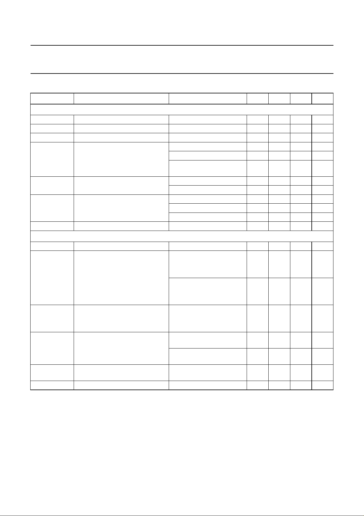
4 QUICK REFERENCE DATA
SYMBOL PARAMETER CONDITIONS MIN. TYP. MAX. UNIT
Supplies
V
DDA(ADC)
V
DDA(DAC)
V
DDD
I
DDA(ADC)
I
DDA(DAC)
I
DDD
T
amb
Analog-to-digital convertor
V
i(rms)
(THD+N)/S
(THD+N)/S
S/N
48
S/N
96
α
cs
ADC analog supply voltage 2.7 3.0 3.6 V
DAC analog supply voltage 2.7 3.0 3.6 V
digital supply voltage 2.7 3.0 3.6 V
ADC analog supply current 1 ADC + 1 PGA enabled − 10.0 − mA
2 ADCs + 2 PGAs enabled − 20.0 − mA
all ADCs + all PGAs
− 200 −µA
power-down
DAC analog supply current operating − 6.0 − mA
DAC power-down − 250 −µA
digital supply current operating − 9.0 − mA
ADC power-down − 4.5 − mA
DAC power-down − 5.5 − mA
ambient temperature −40 − +85 °C
input voltage (RMS value) at 0 dB (FS) digital output − 0.9 − V
total harmonic distortion-plus-noise
48
to signal ratio at fs=48kHz
normal mode
at −1dB −−90 − dB
at −60 dB; A-weighted −−40 − dB
double differential
at −1dB −−93 − dB
at −60 dB; A-weighted −−41 − dB
total harmonic distortion-plus-noise
96
to signal ratio at fs=96kHz
normal mode
at −1dB −−84 − dB
at −60 dB; A-weighted −−39 − dB
signal-to-noise ratio at fs= 48 kHz normal mode;
− 100 − dB
Vi= 0 V; A-weighted
double differential mode;
V
= 0 V; A-weighted
i
signal-to-noise ratio at fs= 96 kHz normal mode;
− 101 − dB
− 99 − dB
Vi= 0 V; A-weighted
channel separation − 100 − dB
2000 Jul 31 4
Philips Semiconductors Product specification
Audio CODEC UDA1342TS
SYMBOL PARAMETER CONDITIONS MIN. TYP. MAX. UNIT
Digital-to-analog convertor
V
o(rms)
output voltage (RMS value) at 0 dB (FS) digital input;
note 1
(THD+N)/S
(THD+N)/S
S/N
48
S/N
96
α
cs
total harmonic distortion-plus-noise
48
to signal ratio at fs=48kHz
total harmonic distortion-plus-noise
96
to signal ratio at fs=96kHz
at 0 dB −−90 − dB
at −60 dB; A-weighted −−40 − dB
at 0 dB −−83 − dB
at −60 dB; A-weighted −−39 − dB
signal-to-noise ratio at fs= 48 kHz code = 0; A-weighted − 100 − dB
signal-to-noise ratio at fs= 96 kHz code = 0; A-weighted − 99 − dB
channel separation − 100 − dB
Note
1. The output voltage of the DAC is proportionally to the DAC power supply voltage.
− 0.9 − V
5 ORDERING INFORMATION
TYPE
NUMBER
NAME DESCRIPTION VERSION
PACKAGE
UDA1342TS SSOP28 plastic shrink small outline package; 28 leads; body width 5.3 mm SOT341-1
2000 Jul 31 5
Philips Semiconductors Product specification
Audio CODEC UDA1342TS
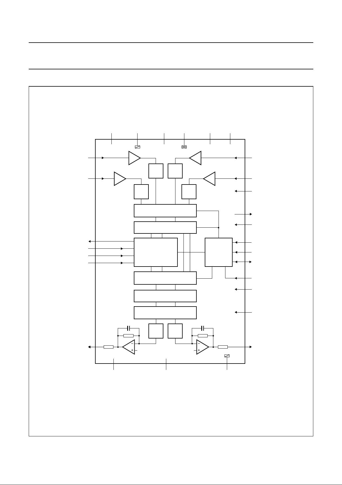
6 BLOCK DIAGRAM
handbook, full pagewidth
VINL2
VINL1
DATAO
BCK
WS
DATAI
V
DDA(ADC)VSSA(ADC)
31
6 8
PGA
2 4
PGA
ADC
UDA1342TS
DC-CANCELLATION FILTER
18
16
17
19
V
ADC
DECIMATION FILTER
DIGITAL MIXER (ADC)
DIGITAL
INTERFACE
DIGITAL MIXER (DAC)
DSP FEATURES
INTERPOLATION FILTER
DDD
10 11
ADC
V
SSD
ADC
PGA
V
ADCPVADCN
75
PGA
L3-BUS/
2
I
C-BUS
INTERFACE
VINR2
VINR1
9
IPSEL
22
STATUS
23
QMUTE
13
L3MODE
14
L3CLOCK
15
L3DATA
21
STATIC
12
SYSCLK
NOISE SHAPER
DAC
VOUTL
26
V
25
DDA(DAC)
28
V
ref
Fig.1 Block diagram.
2000 Jul 31 6
DAC
V
SSA(DAC)
20
TEST1
24
VOUTR
27
MGT016
Philips Semiconductors Product specification
Audio CODEC UDA1342TS
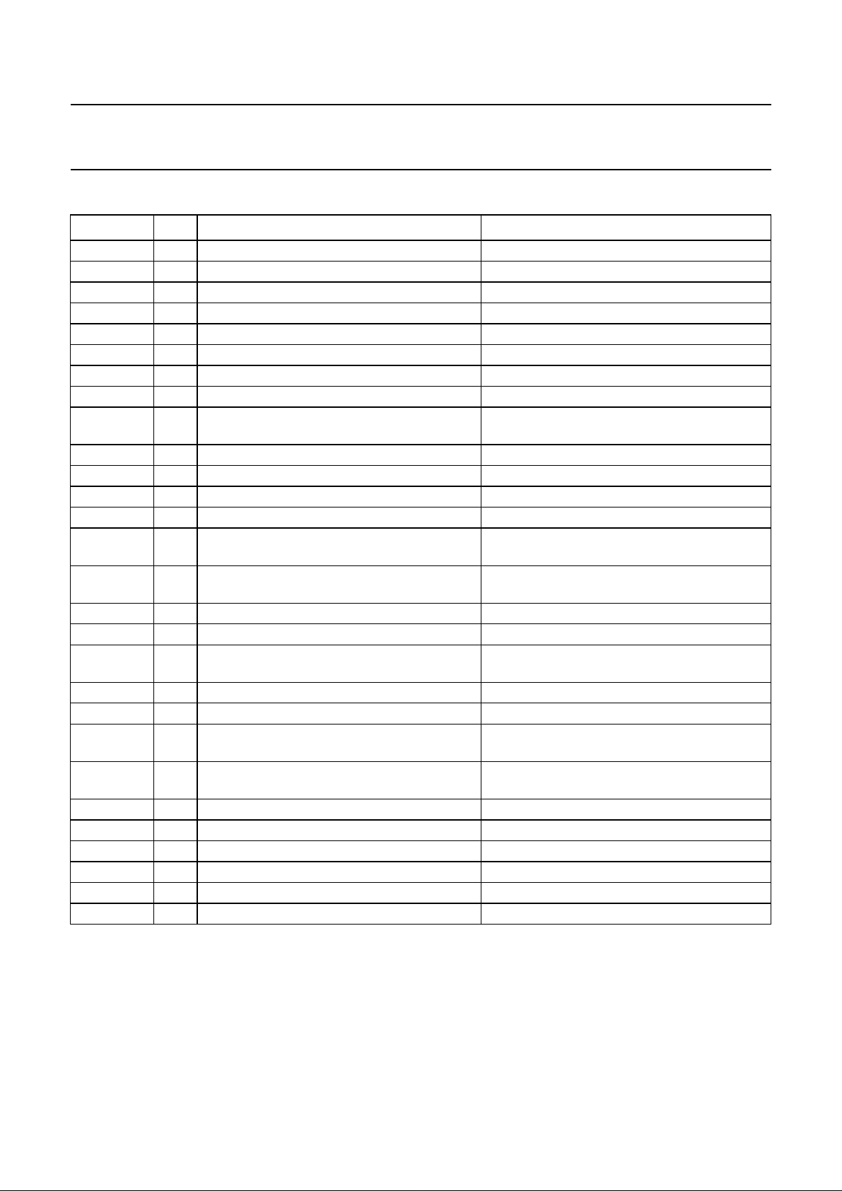
7 PINNING
SYMBOL PIN TYPE DESCRIPTION
V
SSA(ADC)
VINL1 2 analog input pad ADC input left 1
V
DDA(ADC)
VINR1 4 analog input pad ADC input right 1
V
ADCN
VINL2 6 analog input pad ADC input left 2
V
ADCP
VINR2 8 analog input pad ADC input right 2
IPSEL 9 5 V tolerant digital input pad channel select input: input left 1 and right 1 or
V
DDD
V
SSD
SYSCLK 12 5 V tolerant digital input pad system clock input: 256f
L3MODE 13 5 V tolerant digital input pad L3-bus mode input or mode selection input
L3CLOCK 14 5 V tolerant digital input pad L3-bus/I
L3DATA 15 5 V tolerant open drain input/output L3-bus/I
BCK 16 5 V tolerant digital input pad bit clock input
WS 17 5 V tolerant digital input pad word select input
DATAO 18 5 V tolerant 2 mA slew rate controlled digital
DATAI 19 5 V tolerant digital input pad data input
TEST1 20 5 V tolerant digital input pad test control input; to be connected to ground
STATIC 21 5 V tolerant digital input pad mode selection input: static pin control or
STATUS 22 5 V tolerant 2 mA slew rate controlled digital
QMUTE 23 5 V tolerant digital input pad quick mute input
VOUTR 24 analog output pad DAC output right
V
DDA(DAC)
VOUTL 26 analog output pad DAC output left
V
SSA(DAC)
V
ref
1 analog ground pad ADC analog ground
3 analog supply pad ADC analog supply voltage
5 analog pad ADC reference voltage N
7 analog pad ADC reference voltage P
input left 2 and right 2
10 digital supply pad digital supply voltage
11 digital ground pad digital ground
, 384fs, 512fs or 768f
s
2
C-bus clock input or clock selection
input
2
C-bus data input/output or format
selection input
data output
output
L3-bus/I
2
C-bus control
general purpose output
output
25 analog supply pad DAC analog supply voltage
27 analog ground pad DAC analog ground
28 analog pad reference voltage for ADC and DAC
s
2000 Jul 31 7
Philips Semiconductors Product specification
Audio CODEC UDA1342TS
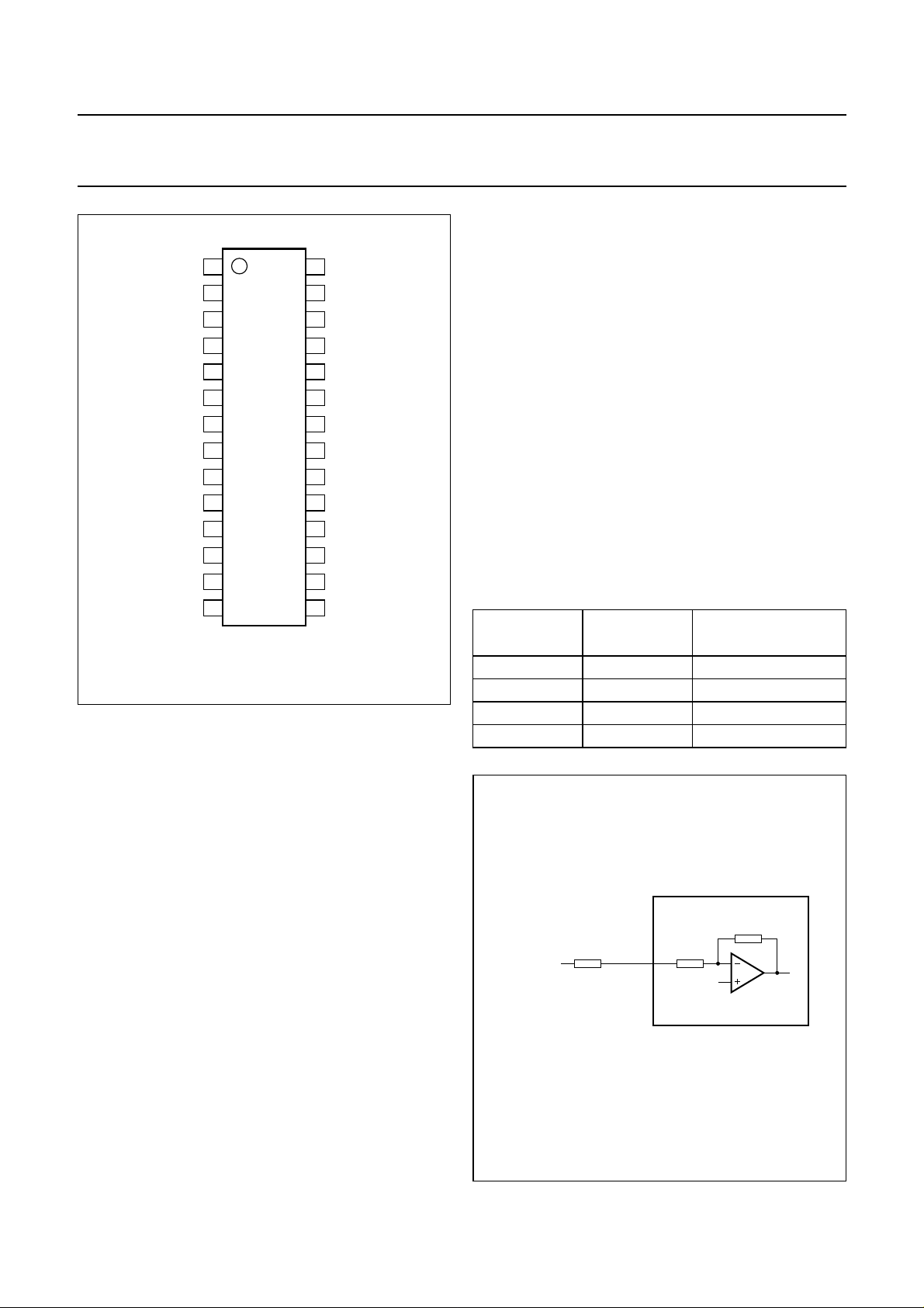
8.2 ADC analog front-end
handbook, halfpage
V
SSA(ADC)
VINL1
V
DDA(ADC)
VINR1
V
ADCN
VINL2
V
ADCP
VINR2
IPSEL
V
V
SYSCLK
L3MODE
L3CLOCK
DDD
SSD
1
2
3
4
5
6
7
UDA1342TS
8
9
10
11
12
13
MGT017
Fig.2 Pin configuration.
8 FUNCTIONAL DESCRIPTION
28
27
26
25
24
23
22
21
20
19
18
17
16
1514
V
ref
V
SSA(DAC)
VOUTL
V
DDA(DAC)
VOUTR
QMUTE
STATUS
STATIC
TEST1
DATAI
DATAO
WS
BCK
L3DATA
The analog front-end of the UDA1342TS consists of two
stereo ADCs with a programmable gain stage (gain from
0 to 24 dB with 3 dB steps)which can be controlledvia the
L3-bus/I2C-bus interface.
8.2.1 APPLICATION WITH 2 V (RMS) INPUT
In applications in which a 2 V (RMS) input signal is used,
a15kΩresistor must be usedinserieswith the input of the
ADC(see Fig.3). This formsa voltage divider together with
the internal ADC resistor and ensures thatonly 1 V (RMS)
maximum is input to the IC. Using this application for a
2 V (RMS) input signal, the gain switch must be set to
0 dB. When a 1 V (RMS)input signal isinput to the ADC in
the same application, the gain switch must be set to 6 dB.
An overview of the maximum input voltages allowed
againstthe presence of an external resistorandthe setting
of the gain switch is given in Table 1.
Table 1 Application modes using input gain stage
RESISTOR
(15 kΩ)
PGA GAIN
MAXIMUM INPUT
VOLTAGE
Present 0 dB 2 V (RMS)
Present 6 dB 1 V (RMS)
Absent 0 dB 1 V (RMS)
Absent 6 dB 0.5 V (RMS)
8.1 System clock
The UDA1342TS operatesin slave mode only, this means
that in allapplications the system must providethe system
clock. The system clock frequency is selectable and
depends on the mode of operation:
• L3-bus/I2C-bus mode: 256fs, 384fs, 512fs or 768f
s
• Static pin mode: 256fs or 384fs.
Thesystemclock must be locked in frequencytothedigital
interface signals.
Remarks:
• The bit clock frequency f
can be up to 128fs, or in
BCK
other words the bit clock frequency is 128 times the
word select frequency fWS or less: f
BCK
≤ 128f
WS
• The WS edge MUST fall on the negative edge of the
BCK signal at all times for proper operation of the digital
interface
• The UDA1342TS operates with sample frequencies
from 16 to 110 kHz, howeverfor a system clock of 768f
s
the sampling frequency must be limited to 55 kHz.
2000 Jul 31 8
handbook, halfpage
input signal
2 V (RMS)
Fig.3 Schematic of ADC front-end.
15 kΩ
VINL1,
VINR1,
VINL2,
VINR2
10 kΩ
V
ref
gain = 0 dB
10 kΩ
2,
4,
6,
8
UDA1342TS
MGT018
Philips Semiconductors Product specification
Audio CODEC UDA1342TS
8.2.2 DOUBLE DIFFERENTIAL MODE
Since the UDA1342TS is equipped with two stereo ADCs,
these two pairs of stereo ADCs can be used to convert a
single stereo signal to a signal with a higher performance
by using the ADCs in the double differential mode.
This mode and the input signals, being channel 1 or 2 as
input to the double differential configuration, can be
selected via the L3-bus/I2C-bus interface.
8.3 Decimation filter (ADC)
Thedecimation from 64fsto1fsisperformed in twostages.
4
xsin
The first stage realizes a characteristic with a
-----------
x
decimation factor of 8. The second stage consists of three
half-bandfilters, each decimating by a factorof 2.The filter
characteristics are shown in Table 2.
Table 2 Decimation filter characteristics
ITEM CONDITION VALUE (dB)
Pass-band ripple 0 to 0.45f
Pass-band droop 0.45f
s
Stop band >0.55f
Dynamic range 0 to 0.45f
s
s
s
±0.01
−0.2
−70
>135
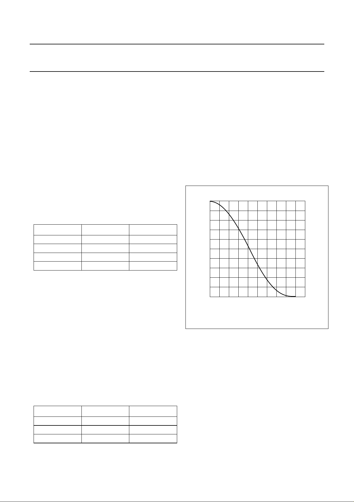
8.6 Mute
Muting the DAC will result in a cosine roll-off soft mute,
using 32 × 32 = 1024 samples in the normal mode: this
results in 24 ms at f
= 44.1 kHz. The cosine roll-off curve
s
is illustrated in Fig.4.
This cosine roll-off functions are implemented in the DAC
data path before the digital mixer and before the master
mute (see Fig.5).
In the L3-bus and I2C-bus mode, the setting of the master
mute can be overruled always by pin QMUTE. This quick
mute uses the same cosine roll-off, but now for only
32 samples: this is 750 µs at fs= 44.1 kHz.
handbook, halfpage
1
mute
factor
0.8
0.6
0.4
MGU119
8.4 Digital mixer (ADC)
The two stereo ADC outputs are mixed with gain
coefficients from +24 to −63.5 dB to be set via the
microcontroller interface.
In front of the mixer there is a DC filter. In order to prevent
clipping, it is needed tofilter out the DC component before
mixing or amplifying the signals.
Themixing function canbe enabled via themicrocontroller
interface.
8.5 Interpolation filter (DAC)
The digital interpolation filter interpolates from 1f
to 64f
s
by means of a cascade of FIR filters. The filter
characteristics are shown in Table 3.
Table 3 Interpolation filter characteristics
ITEM CONDITION VALUE (dB)
Pass-band ripple 0 to 0.45f
Stop band >0.55f
Dynamic range 0 to 0.45f
s
s
s
±0.025
−60
>135
0.2
0
01051525
20
t (ms)
Fig.4 Mute as a function of raised cosine roll-off.
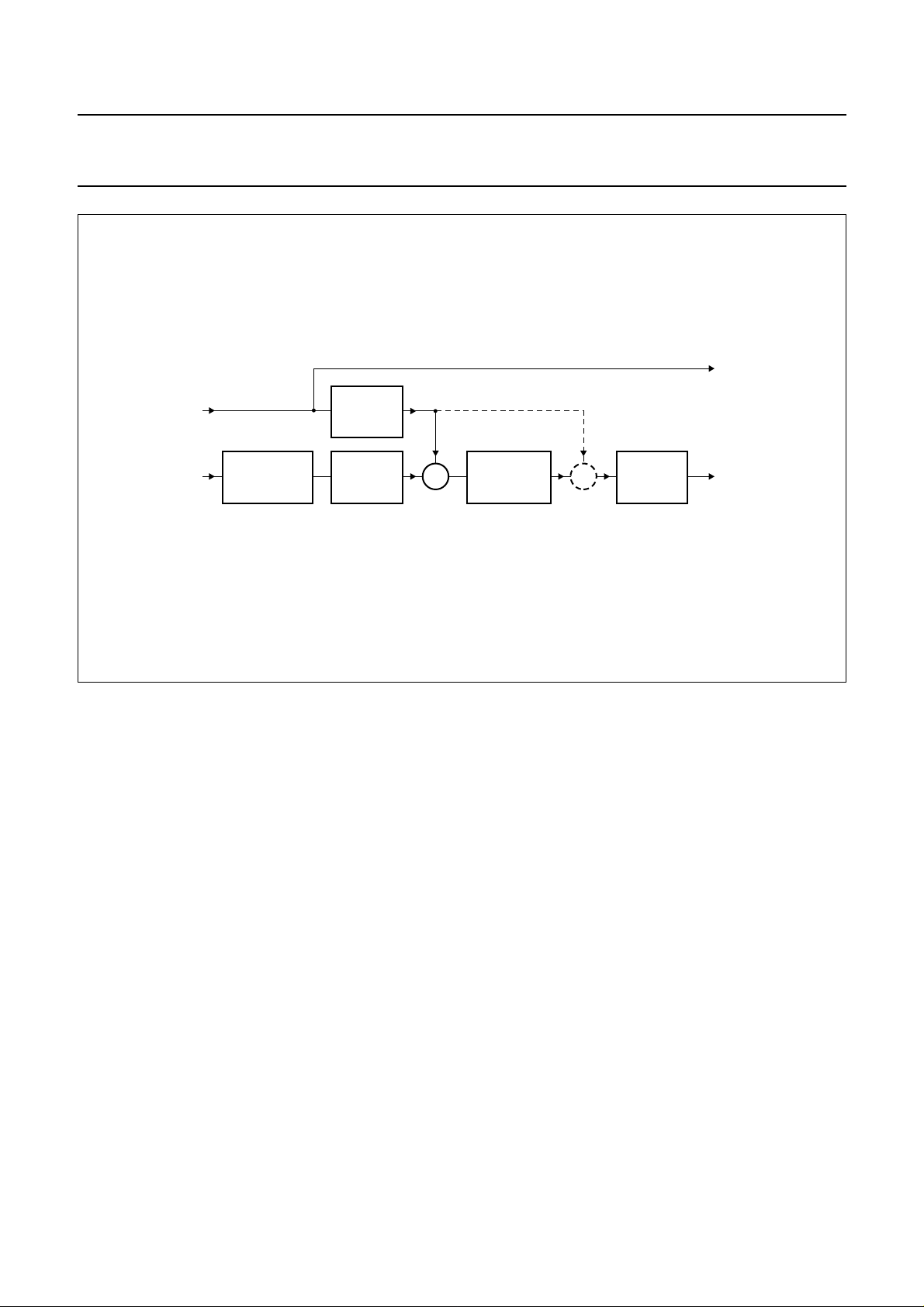
8.7 Digital mixer (DAC)
TheADC output signal and the digitalinterfaceinput signal
can be mixed without an external DSP (see Fig.5).
This mixer can be controlled via the microcontroller
s
interface.
In order to prevent clipping when mixing two 0 dB signals,
thesignals are attenuated digitallyby−6 dB before mixing.
After mixing the signal is gained by 6 dB after the master
volume. This wayclipping at the digital mixeris prevented.
After the 6 dB gain, the signals can clip again, but this
clipping can be removed by decreasing the master
volume.
2000 Jul 31 9
Philips Semiconductors Product specification
Audio CODEC UDA1342TS
handbook, full pagewidth
from
decimation
filter
from
digital
interface
input
DE-EMPHASIS
VOLUME
AND
MUTE
VOLUME
AND
MUTE
+ +
Fig.5 Digital mixer (DAC).
8.8 Noise shaper
The 5th-order noise shaper operates at 64fs. It shifts
in-band quantization noise to frequencies well above the
audio band. This noise shaping technique enables high
signal-to-noise ratios to be achieved. The noise shaper
output is converted into an analog signal using a Filter
Stream Digital-to-Analog Converter (FSDAC).
8.9 Filter stream DAC
The FSDAC is a semi-digital reconstruction filter that
converts the 1-bit data stream of the noise shaper to an
analog output voltage. The filter coefficients are
implemented as current sources and are summed at
virtual ground of the output operational amplifier. In this
way very high signal-to-noise performance and low clock
jitter sensitivity is achieved. A post-filter is not needed due
to the inherent filter function of the DAC. On-board
amplifiers convert the FSDAC output current to an output
voltage signal capable of driving a line output.
to
digital
interface
output
master
BASS BOOST
AND
TREBLE
VOLUME
AND
MUTE
MGT019
to
interpolation
filter
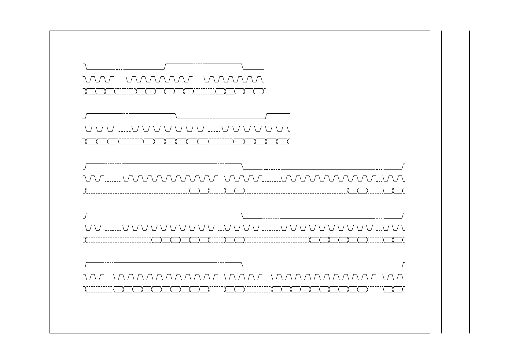
8.10 Digital interface
The UDA1342TS supports the following data input/output
formats for the various modes (see Fig.6).
L3-bus and I2C-bus mode:
• I2S-bus format with data word length of up to 24 bits
• MSB-justifiedserial format with data wordlengthofup to
24 bits
• LSB-justified serial format with data word lengths of
16, 20 or 24 bits
• MSB-justified data output and
LSB-justified 16, 20 and 24 bits data input.
Static pin mode:
• I2S-bus format with data word length of up to 24 bits
• MSB-justified data output and
LSB-justified 16, 20 and 24 bits data input.
The output voltage of the FSDAC is proportionally to the
power supply voltage.
2000 Jul 31 10
This text is here in white to force landscape pages to be rotated correctly when browsing through the pdf in the Acrobat reader.This text is here in
_white to force landscape pages to be rotated correctly when browsing through the pdf in the Acrobat reader.This text is here inThis text is here in
white to force landscape pages to be rotated correctly when browsing through the pdf in the Acrobat reader. white to force landscape pages to be ...
2000 Jul 31 11
handbook, full pagewidth
Philips Semiconductors Product specification
Audio CODEC UDA1342TS
WS
BCK
DATA
WS
BCK
DATA
WS
BCK
DATA
WS
BCK
DATA
MSB B2
MSB B2 MSBLSB LSB MSB B2B2
LEFT
I
LEFT
MSB-JUSTIFIED FORMAT
LEFT
LEFT
MSB B2 B3 B4 B5 B6
RIGHT
3
21> = 812 3
MSB MSBB2
2
S-BUS FORMAT
RIGHT
> = 8 > = 8
321321
16
15 2 1
MSB
B2
16
1518 1720 19 2 1
> = 8
B15
LSB
LSB-JUSTIFIED FORMAT 16 BITS
B19
LSB
LSB-JUSTIFIED FORMAT 20 BITS
RIGHT
16
MSB B2
RIGHT
16
MSB B2 B3 B4 B5 B6
15 2 1
B15 LSB
1518 1720 19 2 1
B19 LSB
WS
BCK
DATA
MSB
LEFT
16
1518 1720 1922 212324 2 1
B23
B2
B3 B4
B5 B6 B7 B8 B9 B10
LSB-JUSTIFIED FORMAT 24 BITS
LSB
MSB
B2
B3 B4
RIGHT
16
B5 B6 B7 B8 B9 B10
1518 1720 1922 212324 21
B23 LSB
MGT020
Fig.6 Serial interface input/output formats.
Philips Semiconductors Product specification
Audio CODEC UDA1342TS
8.11 Sampling speed
The UDA1342TS operates with sample frequencies from
16 to 110 kHz. This range holds for the CODEC as a
whole. The DAC part can be configured in the L3-bus and
I2C-bus mode toaccept 2 times and even 4 times the data
speed (e.g. fsis 96 or 192 kHz), but in these modes not all
of the features can be used.
Some examples of the input oversampling rate settings
are shown in Table 4.
Table 4 Examples of the input oversampling rate settings
SYSTEM
SYSTEM CLOCK
CLOCK
FREQUENCY
SETTING
12.288 MHz (256 × 48 kHz) 256f
22.5792 MHz (512 × 44.1 kHz) 512f
256f
s
s
s
SAMPLING
FREQUENCY
(kHz)
44.1 single speed all
88.2 single speed all
176.4 double speed only master volume and mute
33.8688 MHz (768 × 44.1 kHz) 768f
384f
s
s
44.1 single speed all
88.2 single speed all
176.4 double speed only master volume and mute
Important: in the double speed mode an input signal of
0 dB is allowed, but in the quad speed mode the input
signal must be limited to −6 dB to prevent the system from
clipping.
INPUT OVER-
SAMPLING
FEATURES SUPPORTED
RATE
48 single speed all
96 double speed only master volume and mute
192 quad speed no features
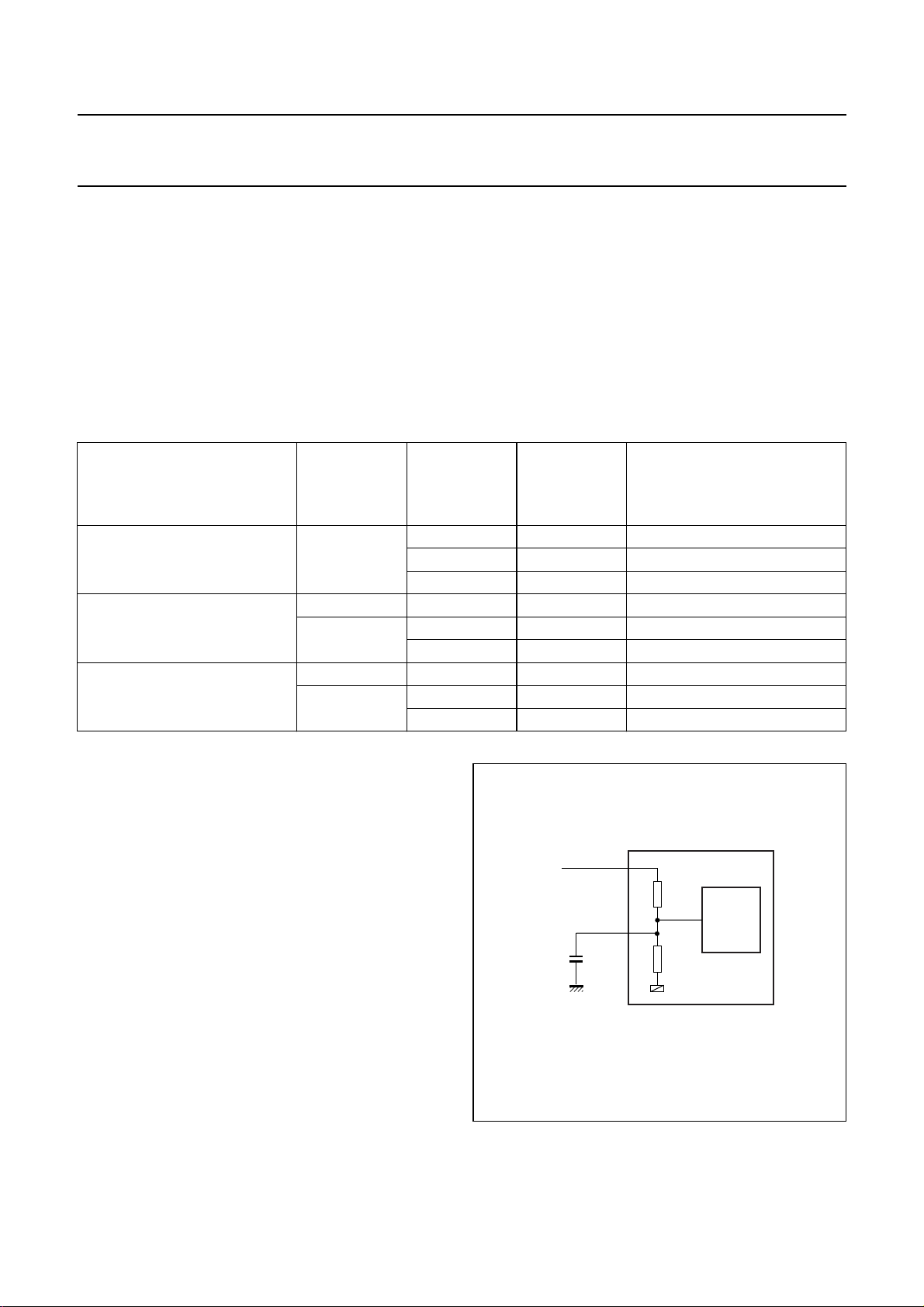
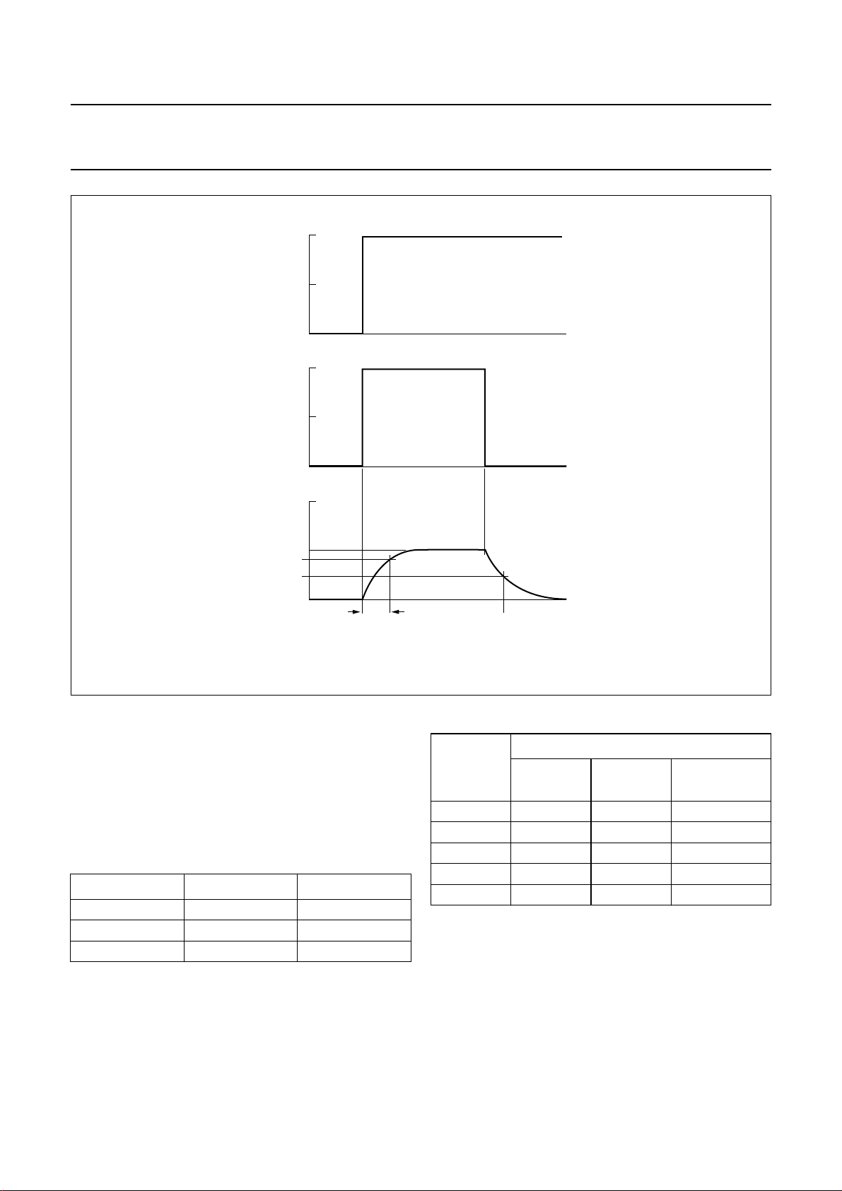
8.12 Power-on reset
The UDA1342TS has an internal Power-on reset circuit
(see Fig.7) which resets the test control block. All the
digital sound processing features and the system
controlling features are set to their default setting in the
L3-bus and I2C-bus mode.
The reset time (see Fig.8) is determined by an external
capacitorwhichis connected between pin V
The reset time should be at least 1 µs for V
When V
DDA(DAC)
again for V
is switched off, the device will be reset
< 0.75 V.
ref
andground.
ref
< 1.25 V.
ref
During the reset time the system clock should be running.
2000 Jul 31 12
handbook, halfpage
3.0 V
V
DDA(DAC)
V
C1 >
10 µF
ref
25
8 kΩ
RESET
28
CIRCUIT
8 kΩ
UDA1342TS
Fig.7 Power-on reset circuit.
MGU001
Philips Semiconductors Product specification
Audio CODEC UDA1342TS
3.0
handbook, halfpage
V
DDD
(V)
1.5
8.13 Control modes
V
DDA(DAC)
(V)
V
(V)
1.25
0.75
ref
3.0
1.5
3.0
1.5
0
0
0
>1 µs
Fig.8 Power-on reset timing.
t
t
t
MGU002
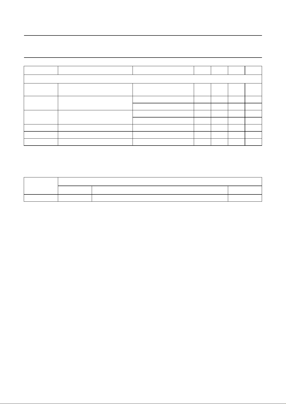
Table 6 Pin function in the selected mode
The control mode can be set with pin STATIC and
pin L3MODE:
• Static pin mode
• I2C-bus mode
• L3-bus mode.
Table 5 Mode selection
PIN STATIC PIN L3MODE SELECTION
LOW − L3-bus mode
2
HIGH LOW I
C-bus mode
HIGH HIGH static pin mode
The pin functions in the various modes are summarized in
Table 6.
2000 Jul 31 13
FUNCTION
PIN NAME
L3-BUS
MODE
I2C-BUS
MODE
STATIC PIN
MODE
L3CLOCK L3CLOCK SCL clock select
L3MODE L3MODE LOW level HIGH level
L3DATA L3DATA SDA format select
QMUTE QMUTE QMUTE format select
IPSEL A0 A0 channel select
2
All features in the L3-bus and I
C-bus mode are explained
in Sections 8.15 and 8.16.
Philips Semiconductors Product specification
Audio CODEC UDA1342TS
8.14 Static pin mode
The controllable features in the static pin mode are:
• System clock frequency
• Data input and output format select
• ADC input channel select.
8.14.1 SYSTEM CLOCK SETTING SELECT
In the static pin mode pin L3CLOCK is used to select the
system clock setting.
Table 7 System clock setting
PIN
L3CLOCK
0 256f
1 384f
SYSTEM CLOCK SETTING
s
s
8.14.2 DIGITAL INTERFACE FORMAT SELECT
In the static pin mode the digital interface audio formats
can be selected via pins L3DATA and QMUTE. The
following interface formats can be selected (see Table 8):
• I2S-bus format with data word length of up to 24 bits
• MSB-justified output format and LSB-justified input
format with data word length of 16, 20 or 24 bits.
Table 8 Data format select in static pin mode
PIN
L3DATA
00I
PIN
QMUTE
INPUT/OUTPUT FORMAT
2
S
0 1 LSB-justified 16 bits input and
MSB-justified output
1 0 LSB-justified 20 bits input and
MSB-justified output
1 1 LSB-justified 24 bits input and
MSB-justified output
8.14.3 ADC INPUT CHANNEL SELECT
In the static pin mode pin IPSEL selects the ADC input
channel.
Table 9 ADC input channel select
PIN
IPSEL
CHANNEL SELECT
0 input channel 1 (pins VINL1 and VINR1)
1 input channel 2 (pins VINL2 and VINR2)
8.15 L3-bus interface
All digital processing features and system controlling
features of the UD1342TS can be controlled by a
microcontroller via the L3-bus interface.
The controllable features are:
• Reset
• System clock frequency
• Data input and output format
• Multi purpose output
• ADC features
– Operation mode control
– Polarity control
– Input amplifier gain control
– Mixer control
– DC filtering.
• DAC features
– Power control
– Polarity control
– Input data oversampling rate
– Mixer position selection
– Mixer control
– Silence detector
– De-emphasis
– Volume
– Flat/min./max. switch
– Bass boost
– Treble
– Mute
– Quick mute mode.
8.15.1 INTRODUCTION
Theexchange of data andcontrol information betweenthe
microcontroller and the UDA1342TS is accomplished
through a serial hardware interface comprising the
following pins:
• L3DATA: microcontroller interface data line
• L3MODE: microcontroller interface mode line
• L3CLOCK: microcontroller interface clock line.
The UDA1342TS acts as a slave receiver or a slave
transmitter. Therefore L3CLOCK and L3MODE lines
transfer only input data and the L3DATA line transfers
bidirectional data.
2000 Jul 31 14
 Loading...