

Philips uda1341ts DATASHEETS
INTEGRATED CIRCUITS
DATA SH EET
UDA1341TS
Economy audio CODEC for
MiniDisc (MD) home stereo and
portable applications
Preliminary specification
File under Integrated Circuits, IC22
1998 Dec 18

Philips Semiconductors Preliminary specification
Economy audio CODEC for MiniDisc (MD)
home stereo and portable applications
CONTENTS
1 FEATURES
1.1 General
1.2 Multiple format data interface
1.3 DAC digital sound processing
1.4 Advanced audio configuration
2 GENERAL DESCRIPTION
3 ORDERING INFORMATION
4 QUICK REFERENCE DATA
5 BLOCK DIAGRAM
6 PINNING
7 FUNCTIONAL DESCRIPTION
7.1 System clock
7.2 Pin compatibility
7.3 Analog front end
7.4 Programmable Gain Amplifier (PGA)
7.5 Analog-to-Digital Converter (ADC)
7.6 Digital Automatic Gain Control (AGC)
7.7 AGC status detection
7.8 Digital mixer
7.9 Decimation filter (ADC)
7.10 Overload detection (ADC)
7.11 Mute (ADC)
7.12 Interpolation filter (DAC)
7.13 Peak detector
7.14 Quick mute
7.15 Noise shaper (DAC)
7.16 Filter Stream Digital-to-Analog Converter
(FSDAC)
7.17 Multiple format input/output interface
7.18 L3-interface
7.19 Address mode
7.20 Data transfer mode
7.21 Programming the sound processing and other
features
7.21.1 STATUS control
7.21.1.1 Reset
7.21.1.2 System clock frequency
7.21.1.3 DC-filter
7.21.1.4 Data input format
7.21.1.5 Output gain switch
7.21.1.6 Input gain switch
7.21.1.7 Polarity of ADC
7.21.1.8 Polarity of DAC
7.21.1.9 Double speed
7.21.1.10 Power control
7.21.2 DATA0 direct control
7.21.2.1 Volume control
7.21.2.2 Bass boost
7.21.2.3 Treble
7.21.2.4 Peak detection position
7.21.2.5 De-emphasis
7.21.2.6 Mute
7.21.2.7 Mode
7.21.3 DATA0 extended programming registers
7.21.3.1 Mixer gain control
7.21.3.2 MIC sensitivity
7.21.3.3 Mixer mode
7.21.3.4 AGC control
7.21.3.5 AGC output level
7.21.3.6 Input channel 2 amplifier gain
7.21.3.7 AGC time constant
7.21.4 DATA1 control
7.21.4.1 Peak level value
8 LIMITING VALUES
9 THERMAL CHARACTERISTICS
10 DC CHARACTERISTICS
11 AC CHARACTERISTICS (ANALOG)
12 AC CHARACTERISTICS (DIGITAL)
13 APPLICATION INFORMATION
14 PACKAGE OUTLINE
15 SOLDERING
15.1 Introduction
15.2 Reflow soldering
15.3 Wave soldering
15.4 Repairing soldered joints
16 DEFINITIONS
17 LIFE SUPPORT APPLICATIONS
UDA1341TS
1998 Dec 18 2
Philips Semiconductors Preliminary specification
Economy audio CODEC for MiniDisc (MD)
home stereo and portable applications
1 FEATURES
1.1 General
• Low power consumption
• 3.0 V power supply
• 256f
• Small package size (SSOP28)
• Partially pin compatible with UDA1340M and
• Fully integrated analog front end including digital AGC
• ADC plus integrated high-pass filter to cancel DC offset
• ADC supports 2 V (RMS value) input signals
• Overload detector for easy record level control
• Separate power control for ADC and DAC
• No analog post filter required for DAC
• Easy application
• Functions controllable via L3-interface.
1.2 Multiple format data interface
• I
• Three combinational data formats with MSB data output
• 1fs input and output format data rate.
1.3 DAC digital sound processing
• Digital dB-linear volume control (low microcontroller
• Digital tone control, bass boost and treble
• Digital de-emphasis for 32, 44.1 or 48 kHz audio sample
• Soft mute.
1.4 Advanced audio configuration
• DAC and ADC polarity control
• Two channel stereo single-ended input configuration
• Microphone input with on-board PGA
, 384fs or 512fs system clock frequencies (f
s
UDA1344TS
2
S-bus, MSB-justified and LSB-justified format
compatible
and LSB 16, 18 or 20 bits data input
load)
frequencies (f
)
s
sys
)
UDA1341TS
• Optional differential input configuration for enhanced
ADC sound quality
• Stereo line output (under microcontroller volume
control)
• Digital peak level detection
• High linearity, dynamic range and low distortion.
2 GENERAL DESCRIPTION
The UDA1341TS is a single-chip stereo Analog-to-Digital
Converter (ADC) and Digital-to-Analog Converter (DAC)
with signal processing features employing bitstream
conversion techniques. Its fully integrated analog front
end, including Programmable Gain Amplifier (PGA) and a
digital Automatic Gain Control (AGC). Digital Sound
Processing (DSP) featuring makes the device an excellent
choice for primary home stereo MiniDisc applications, but
by virtue of its low power and low voltage characteristics it
is also suitable for portable applications such as MD/CD
boomboxes, notebook PCs and digital video cameras.
The UDA1341TS is similar to the UDA1340M and the
UDA1344TS but adds features such as digital mixing of
two input signals and one channel with a PGA and a digital
AGC.
2
The UDA1341TS supports the I
word lengths of up to 20 bits, the MSB-justified data format
with word lengths of up to 20 bits, the LSB-justified serial
data format with word lengths of 16, 18 and 20 bits and
three combinations of MSB data output combined with
LSB 16, 18 and 20 bits data input. The UDA1341TS has
DSP features in playback mode like de-emphasis, volume,
bass boost, treble and soft mute, which can be controlled
via the L3-interface with a microcontroller.
S-bus data format with
3 ORDERING INFORMATION
TYPE
NUMBER
UDA1341TS SSOP28 plastic shrink small outline package; 28 leads; body width 5.3 mm SOT341-1
1998 Dec 18 3
NAME DESCRIPTION VERSION
PACKAGE
Philips Semiconductors Preliminary specification
Economy audio CODEC for MiniDisc (MD)
UDA1341TS
home stereo and portable applications
4 QUICK REFERENCE DATA
SYMBOL PARAMETER CONDITIONS MIN. TYP. MAX. UNIT
Supplies
V
DDA(ADC)
V
DDA(DAC)
V
DDD
I
DDA(ADC)
I
DDA(DAC)
I
DDD
T
amb
Analog-to-digital converter
V
i(rms)
(THD + N)/S total harmonic distortion-plus-noise
S/N signal-to-noise ratio V
α
cs
Programmable gain amplifier
(THD + N)/S total harmonic distortion-plus-noise
S/N signal-to-noise ratio V
Digital-to-analog converter
V
o(rms)
(THD+N)/S total harmonic distortion-plus-noise
S/N signal-to-noise ratio code = 0; A-weighted − 100 − dB
α
cs
ADC analog supply voltage 2.4 3.0 3.6 V
DAC analog supply voltage 2.4 3.0 3.6 V
digital supply voltage 2.4 3.0 3.6 V
ADC analog supply current operation mode − 12.5 − mA
ADC power-down − 6.0 − mA
DAC analog supply current operation mode − 7.0 − mA
DAC power-down − 50 −µA
digital supply current operation mode − 7.0 − mA
operating ambient temperature −20 − +85 °C
input voltage (RMS value) notes 1 and 2 − 1.0 − V
stand-alone mode
to signal ratio
0dB −−85 −80 dB
−60 dB; A-weighted −−37 −33 dB
double differential mode
0dB −−90 −85 dB
−60 dB; A-weighted −−40 −36 dB
= 0 V; A-weighted
i
stand-alone mode − 97 − dB
double differential mode − 100 − dB
channel separation − 100 − dB
1 kHz; f
to signal ratio
= 44.1 kHz
s
0dB −−85 − dB
−60 dB; A-weighted −−37 − dB
= 0 V; A-weighted − 95 − dB
i
output voltage (RMS value) supply voltage = 3 V; note 3 − 900 − mV
0dB −−91 −86 dB
to signal ratio
−60 dB; A-weighted −−40 − dB
channel separation − 100 − dB
Notes
1. The ADC inputs can be used in a 2 V (RMS value) input signal configuration when a resistor of 12 kΩ is used in series
with the inputs and 1 or 2 V (RMS value) input signal operation can be selected via the Input Gain Switch (IGS).
2. The ADC input signal scales inversely proportional with the power supply voltage.
3. The DAC output voltage scales linear with the DAC analog supply voltage.
1998 Dec 18 4
Philips Semiconductors Preliminary specification
Economy audio CODEC for MiniDisc (MD)
home stereo and portable applications
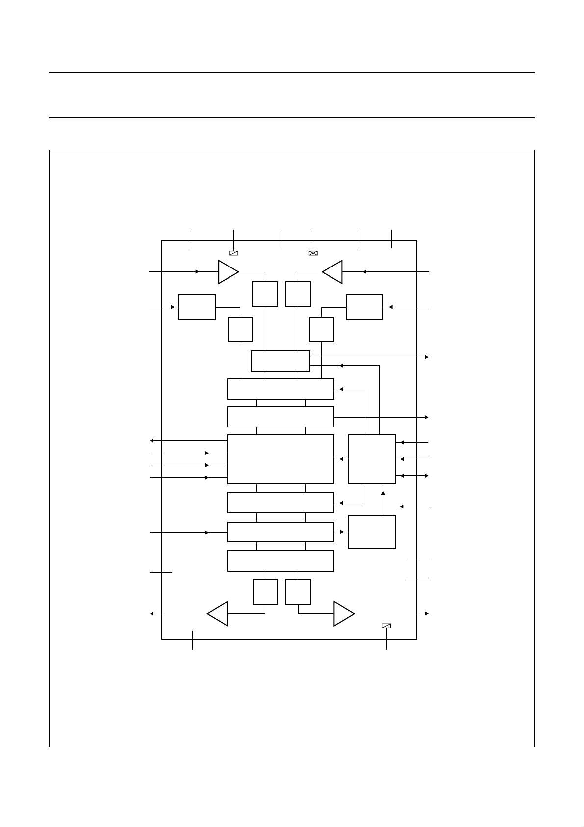
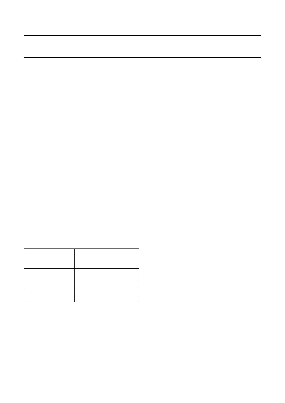
5 BLOCK DIAGRAM
handbook, full pagewidth
VINL2
VINL1
V
DDA(ADC)VSSA(ADC)
31
6 8
PGA PGA
2 4
0 dB/6 dB
SWITCH
ADC1
UDA1341TS
V
DDD
10 11
ADC2
DIGITAL AGC
ADC2
V
SSD
ADC1
V
ADCPVADCN
75
0 dB/6 dB
SWITCH
UDA1341TS
VINR2
VINR1
22
AGCSTAT
DATAO
BCK
WS
DATAI
QMUTE
V
ref
VOUTL
18
16
17
19
23
28
26
V
25
DDA(DAC)
DIGITAL MIXER
DECIMATION FILTER
DIGITAL INTERFACE
DSP FEATURES
INTERPOLATION FILTER
NOISE SHAPER
DAC
DAC
L3-BUS
INTERFACE
PEAK
DETECTOR
V
SSA(DAC)
9
OVERFL
13
L3MODE
14
L3CLOCK
15
L3DATA
12
SYSCLK
20
TEST1
21
TEST2
24
VOUTR
27
MGR427
Fig.1 Block diagram.
1998 Dec 18 5

Philips Semiconductors Preliminary specification
Economy audio CODEC for MiniDisc (MD)
home stereo and portable applications
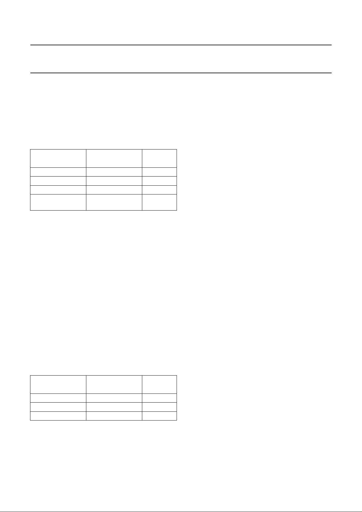
6 PINNING
SYMBOL PIN DESCRIPTION
V
SSA(ADC)
VINL1 2 ADC1 input left
V
DDA(ADC)
VINR1 4 ADC1 input right
V
ADCN
VINL2 6 ADC2 input left
V
ADCP
VINR2 8 ADC2 input right
OVERFL 9 decimation filter overflow output
V
DDD
V
SSD
SYSCLK 12 system clock 256f
L3MODE 13 L3-bus mode input
L3CLOCK 14 L3-bus clock input
1 ADC analog ground
3 ADC analog supply voltage
5 ADC negative reference voltage
7 ADC positive reference voltage
10 digital supply voltage
11 digital ground
, 384fs or 512f
s
s
UDA1341TS
SYMBOL PIN DESCRIPTION
L3DATA 15 L3-bus data input and output
BCK 16 bit clock input
WS 17 word select input
DATAO 18 data output
DATAI 19 data input
TEST1 20 test control 1 (pull-down)
TEST2 21 test control 2 (pull-down)
AGCSTAT 22 AGC status
QMUTE 23 quick mute input
VOUTR 24 DAC output right
V
DDA(DAC)
VOUTL 26 DAC output left
V
SSA(DAC)
V
ref
25 DAC analog supply voltage
27 DAC analog ground
28 ADC and DAC reference voltage
handbook, halfpage
V
SSA(ADC)
V
DDA(ADC)
L3CLOCK
VINL1
VINR1
V
ADCN
VINL2
V
ADCP
VINR2
OVERFL
V
DDD
V
SSD
SYSCLK
L3MODE
1
2
3
4
5
6
7
UDA1341TS
8
9
10
11
12
13
MGR428
28
27
26
25
24
23
22
21
20
19
18
17
16
1514
V
ref
V
SSA(DAC)
VOUTL
V
DDA(DAC)
VOUTR
QMUTE
AGCSTAT
TEST2
TEST1
DATAI
DATAO
WS
BCK
L3DATA
handbook, halfpage
V
SSA(ADC)
V
DDA(ADC)
L3CLOCK
1
VINL1
2
3
VINR1
4
V
V
OVERFL
SYSCLK
L3MODE
5
ADCN
VINL2
6
7
ADCP
VINR2
V
DDD
V
SSD
Marked pins are compatible with UDA1340M
UDA1341TS
8
9
10
11
12
13
14
MGR429
28
27
26
25
24
23
22
21
20
19
18
17
16
15
V
ref
V
SSA(DAC)
VOUTL
V
DDA(DAC)
VOUTR
QMUTE
AGCSTAT
TEST2
TEST1
DATAI
DATAO
WS
BCK
L3DATA
Fig.2 Pin configuration.
1998 Dec 18 6
Fig.3 Compatible pins with UDA1340M.
Philips Semiconductors Preliminary specification
Economy audio CODEC for MiniDisc (MD)
home stereo and portable applications
7 FUNCTIONAL DESCRIPTION
7.1 System clock
The UDA1341TS accommodates slave mode only, this
means that in all applications the system devices must
provide the system clock. The system frequency is
selectable. The options are 256f
The system clock must be locked in frequency to the digital
interface signals.
7.2 Pin compatibility
The UDA1341TS is partially pin compatible with the
UDA1340M and UDA1344TS, making an upgrade of a
printed-circuit board from UDA1340M to UDA1341TS
easier. The pins that are compatible with the UDA1340M
are marked in Fig.3.
7.3 Analog front end
The analog front end of the UDA1341TS consists of two
stereo ADCs with a Programmable Gain Amplifier (PGA)
in channel 2. The PGA is intended to pre-amplify a
microphone signal applied to the input channel 2.
Input channel 1 has a selectable 0 or 6 dB gain stage, to
be controlled via the L3-interface. In this way, input signals
of 1 V (RMS value) or 2 V (RMS value) e.g. from a
CD source can be supported using an external resistor of
12 kΩ in series with the input channel 1. The application
modes are given in Table 1.
Table 1 Application modes using input gain stage
RESISTOR
(12 kΩ)
Present 0 dB 2 V (RMS value) input signal;
Present 6 dB 1 V (RMS value) input signal
Absent 0 dB 1 V (RMS value) input signal
Absent 6 dB 0.5 V (RMS value) input signal
Note
1. If there is no need for 2 V (RMS value) input signal
support, the external resistor should not be used.
INPUT
GAIN
SWITCH
, 384fs or 512fs.
s
MAXIMUM INPUT VOLTAGE
note 1
UDA1341TS
7.5 Analog-to-Digital Converter (ADC)
The stereo ADC of the UDA1341TS consists of two
3rd-order Sigma-Delta modulators. They have a modified
Ritchie-coder architecture in a differential switched
capacitor implementation. The over-sampling ratio is 128.
7.6 Digital Automatic Gain Control (AGC)
Input channel 2 has a digital AGC to compress the
dynamic range when a microphone signal is applied to
input channel 2. The digital AGC can be switched on and
off via the L3-interface. In the on state the AGC
compresses the dynamic range of the input signal of input
channel 2. Via the L3-interface the user can set the
parameters of the AGC: attack time, decay time and output
level. When the AGC is set off via the L3-interface, the gain
of input channel 2 can be set manually. In this case the
gain of the PGA and digital AGC are combined. The range
of the gain of the input channel 2 is from −3 to +60.5 dB in
steps of 0.5 dB.
7.7 AGC status detection
The AGCSTAT signal from the digital AGC is HIGH when
the gain level of the AGC is below 8 dB. This signal can be
used to give the PGA a new gain setting via the
L3-interface and to power e.g. a LED.
7.8 Digital mixer
The two stereo ADCs (including the AGC) can be used in
four modes:
• ADC1 only mode (for line input); input channel 2 is off
• ADC2 only mode, including PGA and digital AGC (for
microphone input); input channel 1 is off
• ADC1 + ADC2 mixer mode, including PGA and AGC
• ADC1 and ADC2 double differential mode (improved
ADC performance).
Important: In order to prevent crosstalk between the line
inputs no signal should be applied to the microphone input
in the double differential mode.
In all modes (except the double differential mode) a
reference voltage is always present at the input of the
ADC. However, in the double differential mode there is no
reference voltage present at the microphone input.
7.4 Programmable Gain Amplifier (PGA)
The PGA can be set via the L3-interface at the gain
settings: −3, 0, 3, 9, 15, 21 or 27 dB.
1998 Dec 18 7
In the mixer mode, the output signals of both ADCs in
channel 1 and channel 2 (after the digital AGC) can be
mixed with coefficients that can be set via the L3-interface.
The range of the mixer coefficients is from 0 to −∞ dB in
1.5 dB steps.
Philips Semiconductors Preliminary specification
Economy audio CODEC for MiniDisc (MD)
home stereo and portable applications
7.9 Decimation filter (ADC)
The decimation from 128f
The first stage realizes 3rd order characteristic,
decimating by 16. The second stage consists of
3 half-band filters, each decimating by a factor of 2.
Table 2 Decimation filter characteristics
ITEM CONDITIONS
Passband ripple 0 to 0.45f
Stop band >0.55f
Dynamic range 0 to 0.45f
Overall gain input channel 1;
7.10 Overload detection (ADC)
This name is convenient but a little inaccurate. In practice
the output is used to indicate whenever that output data, in
either the left or right channel, is bigger than −1 dB (actual
figure is −1.16 dB) of the maximum possible digital swing.
If this condition is detected the OVERFL output is forced
HIGH for at least 512f
This time-out is reset for each infringement.
7.11 Mute (ADC)
On recovery from power-down or switching on of the
system clock, the serial data output DATAO is held LOW
until valid data is available from the decimation filter.
is performed in two stages.
s
sin x
----------- x
VALUE
(dB)
s
s
s
±0.05
−60
108
−1.16
0 dB input
cycles (11.6 ms at fs= 44.1 kHz).
s
UDA1341TS
The peak level detector is implemented as a peak-hold
detector, which means that the highest sound level is hold
until the peak level is read out via the L3-interface. After
read-out the peak level registers are reset.
7.14 Quick mute
A hard mute can be activated via the static pin QMUTE.
When QMUTE is set HIGH, the output signal is instantly
muted to zero. Setting QMUTE to LOW, the mute is
instantly in-activated.
7.15 Noise shaper (DAC)
The 3rd-order noise shaper operates at 128f
in-band quantization noise to frequencies well above the
audio band. This noise shaping technique allows for high
signal-to-noise ratios. The noise shaper output is
converted into an analog signal using a filter stream
digital-to-analog converter.
7.16 Filter Stream Digital-to-Analog Converter (FSDAC)
The FSDAC is a semi-digital reconstruction filter that
converts the 1-bit data stream of the noise shaper to an
analog output voltage. The filter coefficients are
implemented as current sources and are summed at
virtual ground of the output operational amplifier. In this
way very high signal-to-noise performance and low clock
jitter sensitivity is achieved. A post filter is not needed due
to the inherent filter function of the DAC. On-board
amplifiers convert the FSDAC output current to an output
voltage signal capable of driving a line output.
. It shifts
s
7.12 Interpolation filter (DAC)
The digital filter interpolates from 1f
to 128fs by means of
s
a cascade of a recursive filter and a Finite Impulse
Response (FIR) filter.
Table 3 Interpolation filter characteristics
ITEM CONDITIONS
Passband ripple 0 to 0.45f
Stop band >0.55f
s
Dynamic range 0 to 0.45f
s
s
VALUE
(dB)
±0.03
−50
108
7.13 Peak detector
In the playback path a peak level detector is build in.
The position of the peak detection can be set via the
L3-interface to either before or after the sound features.
1998 Dec 18 8
7.17 Multiple format input/output interface
The UDA1341TS supports the following data formats:
2
• I
S-bus with word length up to 20 bits
• MSB-justified serial format with word length up to 20 bits
• LSB-justified serial format with word length of
16, 18 or 20 bits
• MSB data output with LSB 16, 18 or 20 bits input.
Left and right data-channel words are time multiplexed.
The formats are illustrated in Fig.4.
The UDA1341TS allows for double speed data monitoring
purposes. In this case the sound features bass boost,
treble and de-emphasis cannot be used. However, volume
control and soft-mute can still be controlled. The double
speed monitoring option can be set via the L3-interface.
The bit clock frequency must be 64 times word select
frequency or less, so f
≤ 64 × fWS.
BCK

This text is here in white to force landscape pages to be rotated correctly when browsing through the pdf in the Acrobat reader.This text is here in
o
_white to force landscape pages to be rotated correctly when browsing through the pdf in the Acrobat reader.This text is here inThis text is here in
white to force landscape pages to be rotated correctly when browsing through the pdf in the Acrobat reader. white to force landscape pages to be ...
1998 Dec 18 9
WS
BCK
DATA
LEFT
>=8 >=8
MSB B2 MSBLSB LSB MSBB2
RIGHT
321321
INPUT FORMAT I
ok, full pagewidth
2
S-BUS
Philips Semiconductors Preliminary specification
Economy audio CODEC for MiniDisc (MD)
home stereo and portable applications
WS
BCK
DATA
WS
BCK
DATA
WS
BCK
DATA
WS
BCK
DATA
LEFT
1321
>=8 >=8
MSB B2 MSBLSB LSB MSB B2B2
LEFT
1516 1
MSB LSBB2
LEFT
MSB B2 B3 B4
LEFT
MSB B2 B3 B4 B5 B6
RIGHT
32
MSB-JUSTIFIED FORMAT
2
B15
LSB-JUSTIFIED FORMAT 16 BITS
215161718 1
LSB
B17
LSB-JUSTIFIED FORMAT 18 BITS
2151617181920 1
LSB
B19
LSB-JUSTIFIED FORMAT 20 BITS
RIGHT
MSB LSBB2 B15
RIGHT
MSB B2 B3 B4
RIGHT
MSB B2 B3 B4 B5 B6
B17
B19
21516 1
215161718 1
LSB
2151617181920 1
UDA1341TS
LSB
MGG841
Fig.4 Serial interface formats.

Philips Semiconductors Preliminary specification
Economy audio CODEC for MiniDisc (MD)
home stereo and portable applications
7.18 L3-interface
The UDA1341TS has a microcontroller input mode. In the
microcontroller mode, all the digital sound processing
features and the system controlling features can be
controlled by the microcontroller.
The controllable features are:
• Reset
• System clock frequency
• Power control
• DAC gain switch
• ADC input gain switch
• ADC/DAC polarity control
• Double speed playback
• De-emphasis
• Volume
• Mode switch
• Bass boost
• Treble
• Mute
• MIC sensitivity control
• AGC control
• Input amplifier gain control
• Digital mixer control
• Peak detection position.
Via the L3-interface the peak level value of the signal in the
DAC path can be read out from the UDA1341TS to the
microcontroller.
The exchange of data and control information between the
microcontroller and the UDA1341TS is accomplished
through a serial hardware L3-interface comprising the
following pins:
• L3DATA: microcontroller interface data line
• L3MODE: microcontroller interface mode line
• L3CLOCK: microcontroller interface clock line.
Information transfer through the microcontroller bus is
organized in accordance with the so called ‘L3’ format, in
which two different modes of operation can be
distinguished: address mode and data transfer mode.
UDA1341TS
The address mode is required to select a device
communicating via the L3-bus and to define the
destination registers for the data transfer mode.
Data transfer can be in both directions: input to the
UDA1341TS to program its sound processing and system
controlling features and output from the UDA1341TS to
provide the peak level value.
7.19 Address mode
The address mode is used to select a device for
subsequent data transfer and to define the destination
registers. The address mode is characterized by L3MODE
being LOW and a burst of 8 pulses on L3CLOCK,
accompanied by 8 data bits. The fundamental timing is
shown in Fig.5.
Data bits 7 to 2 represent a 6-bit device address, with bit 7
being the MSB and bit 2 the LSB. The address of the
UDA1341TS is 000101.
Data bits 0 to 1 indicate the type of the subsequent data
transfer as shown in Table 4.
In the event that the UDA1341TS receives a different
address, it will deselect its microcontroller interface logic.
7.20 Data transfer mode
The selection activated in the address mode remains
active during subsequent data transfers, until the
UDA1341TS receives a new address command.
The fundamental timing of data transfers is essentially the
same as the timing in the address mode and is given in
Fig.6.
Note that ‘L3DATA write’ denotes data transfer from the
microcontroller to the UDA1341TS and ‘L3DATA peak
read’ denotes data transfer in the opposite direction.
The maximum input clock and data rate is 64f
All transfers are byte-wise, i.e. they are based on groups
of 8 bits. Data will be stored in the UDA1341TS after the
eighth bit of a byte has been received.
A multibyte transfer is illustrated in Fig.7.
.
s
1998 Dec 18 10
 Loading...