

Philips UDA1340M-N1 Datasheet

DATA SH EET
Preliminary specification
Supersedes data of 1997 May 20
File under Integrated Circuits, IC01
1997 Jul 09
INTEGRATED CIRCUITS
UDA1340
Low-voltage low-power stereo
audio CODEC with DSP features
1997 Jul 09 2
Philips Semiconductors Preliminary specification
Low-voltage low-power stereo audio
CODEC with DSP features
UDA1340
FEATURES
General
• Low power consumption
• 3.0 V power supply
• 256, 384 and 512f
s
system clock
• Small package size (SSOP28)
• ADC plus integrated high pass filter to cancel DC offset
• Overload detector for easy record level control
• Separate power control for ADC and DAC
• Integrated digital filter plus DAC
• No analog post filter required for DAC
• Easy application
• Functions controllable by microcontroller interface.
Multiple format input interface
• I
2
S-bus, MSB-justified and LSB-justified format
compatible
• 1fs input and output format data rate.
DAC digital sound processing
• Digital volume control
• Digital tone control, bass boost and treble
• dB-linear volume and tone control (low microcontroller
load)
• Digital de-emphasis for 32, 44.1 and 48 kHz f
s
• Soft mute.
Advanced audio configuration
• Stereo single-ended input configuration
• Stereo line output (under microcontroller volume
control)
• Power-down click prevention circuitry
• High linearity, dynamic range, low distortion.
GENERAL DESCRIPTION
The UDA1340 is a single-chip stereo Analog-to-Digital
Converter (ADC) and Digital-to-Analog Converter (DAC)
with signal processing features employing bitstream
conversion techniques. The low power consumption and
low voltage requirements make the device eminently
suitable for use in low-voltage low-power portable digital
audio equipment which incorporates recording and
playback functions.
The UDA1340 supports the I
2
S-bus data format with word
lengths of up to 20 bits, the MSB-justified data format with
word lengths of up to 20 bits and the LSB justified serial
data format with word lengths of 16, 18 and 20 bits.
The UDA1340 has special sound processing features in
playback mode, de-emphasis, volume, bass boost, treble,
and soft mute, which can be controlled via the
microcontroller interface.
ORDERING INFORMATION
TYPE
NUMBER
PACKAGE
NAME DESCRIPTION VERSION
UDA1340M SSOP28 plastic shrink small outline package; 28 leads; body width 5.3 mm SOT341-1
1997 Jul 09 3
Philips Semiconductors Preliminary specification
Low-voltage low-power stereo audio
CODEC with DSP features
UDA1340
QUICK REFERENCE DATA
SYMBOL PARAMETER CONDITIONS MIN. TYP. MAX. UNIT
Supply
V
DDA(ADC)
ADC analog supply voltage 2.7 3.0 3.6 V
V
DDA(DAC)
DAC analog supply voltage 2.7 3.0 3.6 V
V
DDO
operational amplifiers supply voltage 2.7 3.0 3.6 V
V
DDD
digital supply voltage 2.7 3.0 3.6 V
I
DDA(ADC)
ADC supply current − 4.5 − mA
I
DDA(DAC)
DAC supply current − 3.5 − mA
I
DDO
operational amplifier supply current − 4 − mA
I
DDD
digital supply current − 6 − mA
I
PD(ADC)
digital ADC power-down supply current − 3 − mA
I
PD(DAC)
digital DAC power-down supply current − 3 − mA
T
amb
operating ambient temperature −20 − +85
°
C
Analog-to-digital converter
V
I(rms)
input voltage (RMS value) − 0.8 − V
(THD + N)/S total harmonic distortion plus
noise-to-signal ratio
at 0 dB −−85 −80 dB
at −60 dB; A-weighted −−35 −30 dBA
S/N signal-to-noise ratio V
i
= 0 V; A-weighted − 95 − dBA
α
cs
channel separation − 100 − dB
Digital-to-analog converter
V
o(rms)
output voltage (RMS value) − 0.8 − V
(THD + N)/S total harmonic distortion plus
noise-to-signal ratio
at 0 dB −−85 −80 dB
at −60 dB; A-weighted −−35 − dBA
S/N signal-to-noise ratio code = 0; A weighted − 100 − dBA
α
cs
channel separation − 100 − dB
Power performance
P
ADDA
power consumption in record and
playback mode
− 54 − mW
P
DA
power consumption in playback only
mode
− 33 − mW
P
AD
power consumption in record only
mode
− 27 − mW
P
PD
power consumption in power-down
mode
− 6 − mW
1997 Jul 09 4
Philips Semiconductors Preliminary specification
Low-voltage low-power stereo audio
CODEC with DSP features
UDA1340
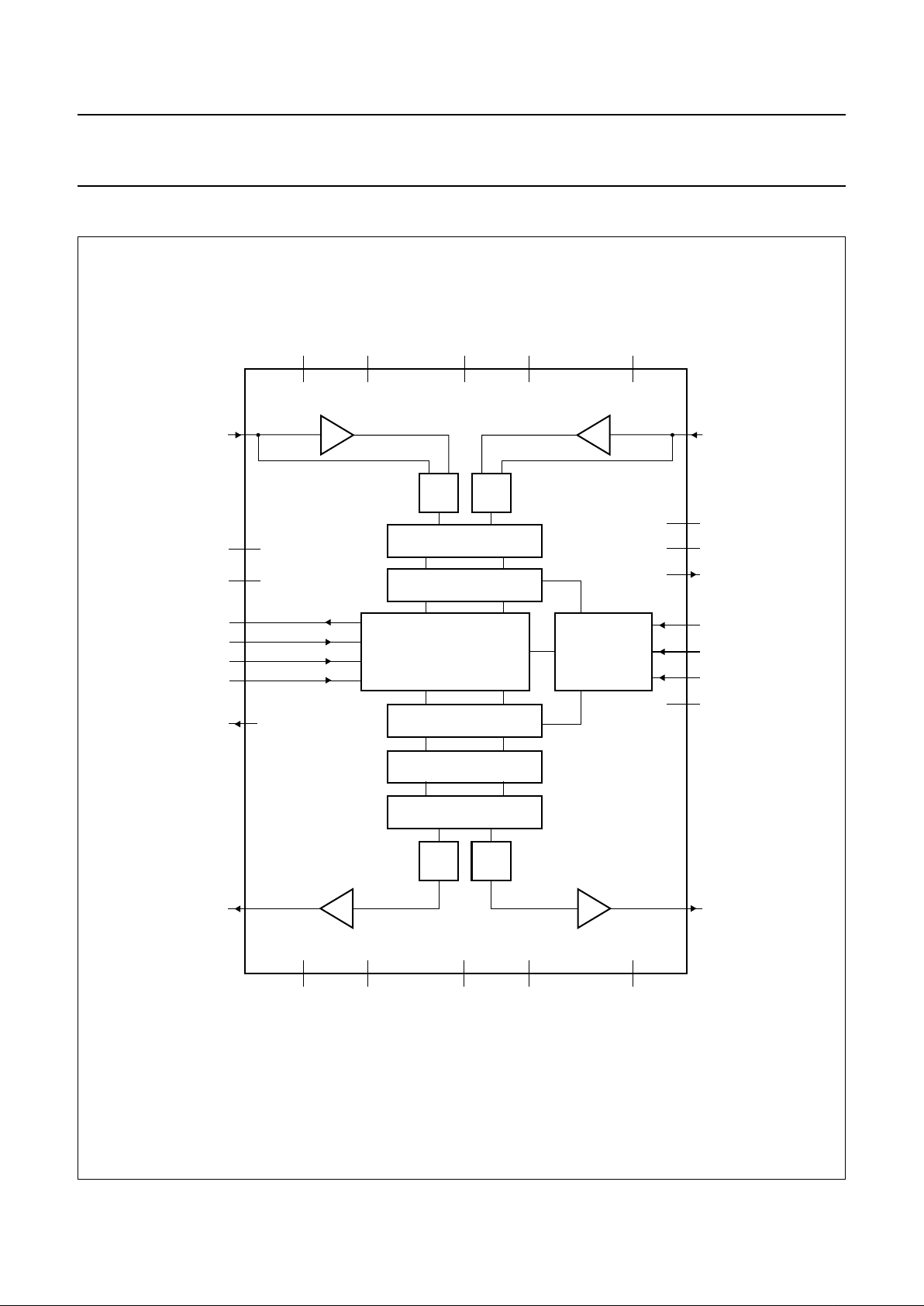
BLOCK DIAGRAM
Fig.1 Block diagram.
handbook, full pagewidth
MGG839
ADC
3 5
10
11
18
16
17
19
25 27 23 22
12
15
14
13
20
21
8
VINL
V
DDD
V
SSD
DATAO
BCK
WS
DATAI
OVERFL
VOUTL
28
24
9
26
VOUTR
SYSCLK
L3DATA
L3CLOCK
L3MODE
TEST3
TEST2
TEST1
VINR
21
76 4
DECIMATION FILTER
DC-CANCELLATION FILTER
DIGITAL INTERFACE
L3-BUS
INTERFACE
ADC
DAC
V
ref(D)
V
DDO
V
SSO
DAC
INTERPOLATION FILTER
NOISE SHAPER
DSP FEATURES
V
DDA(ADC)VSSA(ADC)
V
ADCP
V
ADCN
V
ref(A)
UDA1340
V
DDA(DAC)VSSA(DAC)

1997 Jul 09 5
Philips Semiconductors Preliminary specification
Low-voltage low-power stereo audio
CODEC with DSP features
UDA1340
PINNING
SYMBOL PIN
Description
V
SSA(ADC)
1 ADC analog ground
V
DDA(ADC)
2 ADC analog supply voltage
VINL 3 ADC input left
V
ref(A)
4 ADC reference voltage
VINR 5 ADC input right
V
ADCN
6 ADC negative reference voltage
V
ADCP
7 ADC positive reference voltage
TEST1 8 test control 1 (pull-down)
OVERFL 9 overload flag output
V
DDD
10 digital supply voltage
V
SSD
11 digital ground
SYSCLK 12 system clock 256, 384 or 512f
s
L3MODE 13 L3-bus mode input
L3CLOCK 14 L3-bus clock input
L3DATA 15 L3-bus data input
BCK 16 bit clock input
WS 17 word selection input
DATAO 18 data output
DATAI 19 data input
TEST3 20 test output
TEST2 21 test control 2 (pull-down)
V
SSA(DAC)
22 DAC analog ground
V
DDA(DAC)
23 DAC analog supply voltage
VOUTR 24 DAC output right
V
DDO
25 operational amplifier supply voltage
VOUTL 26 DAC output left
V
SSO
27 operational amplifier ground
V
ref(D)
28 DAC reference voltage
Fig.2 Pin configuration.
handbook, halfpage
V
SSA(ADC)
V
DDA(ADC)
VINL
V
ref(A)
VINR
V
ADCN
V
ADCP
TEST1
OVERFL
V
DDD
V
SSD
SYSCLK
L3MODE
L3CLOCK
V
ref(D)
V
SSO
VOUTL
V
DDO
V
DDA(DAC)
V
SSA(DAC)
VOUTR
TEST2
TEST3
DATAI
DATAO
WS
BCK
L3DATA
1
2
3
4
5
6
7
8
9
10
11
12
13
28
27
26
25
24
23
22
21
20
19
18
17
16
1514
UDA1340
MGG838

1997 Jul 09 6
Philips Semiconductors Preliminary specification
Low-voltage low-power stereo audio
CODEC with DSP features
UDA1340
FUNCTIONAL DESCRIPTION
System clock
The UDA1340 accommodates slave mode only, this
means that in all applications the system devices must
provide the system clock. The system frequency is
selectable. The options are 256f
s
, 384fs and 512fs.
The system clock must be locked in frequency to the digital
interface input signals.
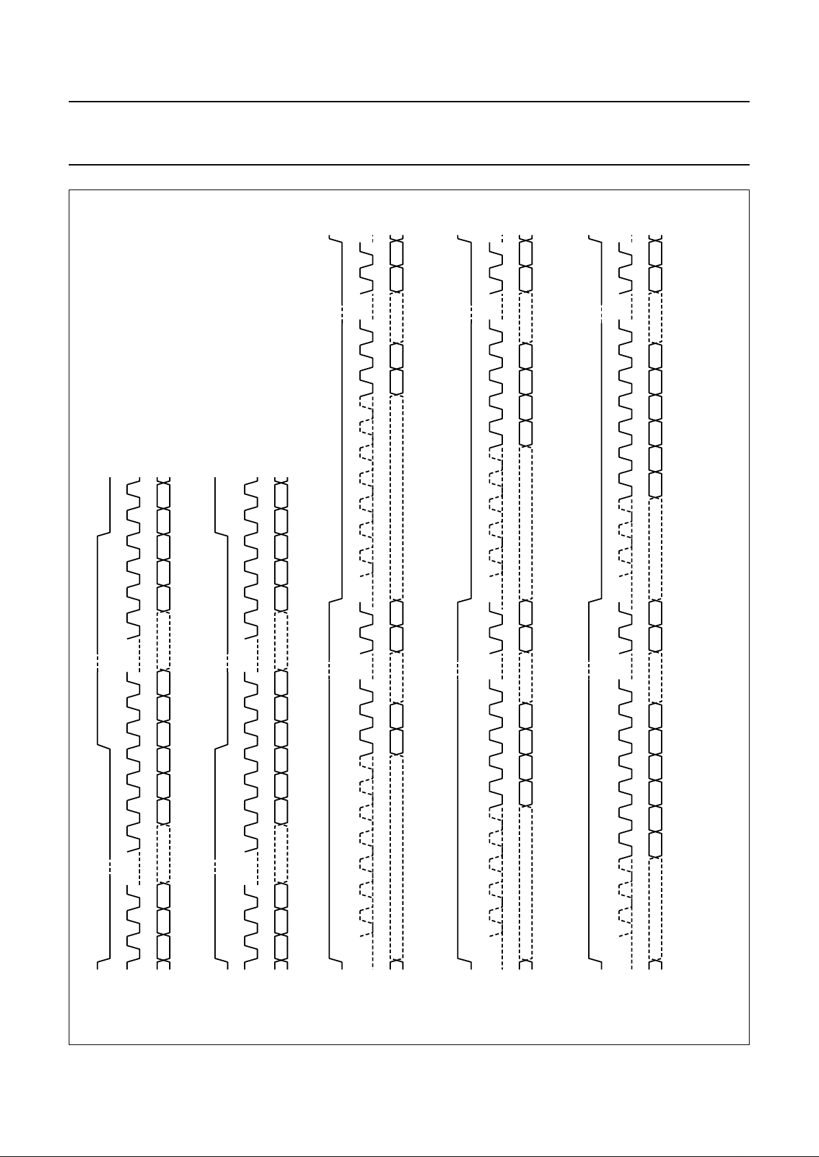
Multiple format input/output interface
The UDA1340 supports the following data input/output
formats:
• I
2
S-bus with data word length of up to 20 bits
• MSB justified serial format with data word length of up to
20 bits
• LSB justified serial format with data word lengths of
16, 18 or 20 bits.
The formats are illustrated in Fig.3. Left and right
data-channel words are time multiplexed.
Analog-to-Digital Converter (ADC)
The stereo ADC of the UDA1340 consists of two
third-order Sigma-Delta modulators. They have a modified
Ritchie-coder architecture in a differential switched
capacitor implementation. The over-sampling ratio is 128.
Decimation filter (ADC)
The decimation from 128f
s
is performed in two stages.
The first stage realizes 3rd-order characteristic. This
filter decreases the sample rate by 16. The second stage,
an FIR filter, consists of 3 half-band filters, each
decimating by a factor of 2.
Table 1 Decimation filter characteristics
ITEM CONDITION VALUE (dB)
Passband Ripple 0 − 0.45f
s
±0.05
Stop band >0.55f
s
−60
Dynamic range 0 − 0.45f
s
108
Gain overall −1.16
sin x
x
----------- -
DC cancellation filter (ADC)
An optional IIR high-pass filter is provided to remove
unwanted DC components. The operation is selected by
the microcontroller via the L3-bus. The filter characteristics
are given in Table 2.
Table 2 DC cancellation filter characteristics
Mute (ADC)
On recovery from power-down or switching on of the
system clock, the serial data output DATAO is held LOW
until valid data is available from the decimation filter. This
time depends on whether the DC cancellation filter is
selected:
DC cancel off: time = , t = 23.2 ms when
f
s
= 44.1 kHz
DC cancel on: time = , t = 279 ms when
f
s
= 44.1 kHz
Overload detection (ADC)
In practice the output is used to indicate whenever the
output data, in either the left or right channel, is greater
than −1 dB (actual figure is −1.16 dB) of the maximum
possible digital swing. When this condition is detected the
OVERFL output is forced HIGH for at least 512f
s
cycles
(11.6 ms at fs= 44.1 kHz). This time-out is reset for each
infringement.
ITEM CONDITION VALUE (dB)
Passband ripple none
Passband gain 0
Droop at 0.00045f
s
0.031
Attenuation at DC at 0.00000036f
s
>40
Dynamic range 0 − 0.45f
s
>110
1024
f
s
------------ -
12288
f
s
----------------

1997 Jul 09 7
Philips Semiconductors Preliminary specification
Low-voltage low-power stereo audio
CODEC with DSP features
UDA1340
Interpolation filter (DAC)
The digital filter interpolates from 1fsto 128fs by means of
a cascade of a recursive filter and an FIR filter.
Table 3 Interpolation filter characteristics
Noise shaper (DAC)
The 3rd-order noise shaper operates at 128f
s
. It shifts
in-band quantization noise to frequencies well above the
audio band. This noise shaping technique enables high
signal-to-noise ratios to be achieved. The noise shaper
output is converted into an analog signal using a filter
stream digital-to-analog converter.
ITEM CONDITION VALUE (dB)
Passband ripple 0 − 0.45f
s
±0.03
Stop band >0.55f
s
−50
Dynamic range 0 − 0.45f
s
108
Gain DC −3.5
The Filter Stream DAC (FSDAC)
The FSDAC is a semi-digital reconstruction filter that
converts the 1-bit data stream of the noise shaper to an
analog output voltage. The filter coefficients are
implemented as current sources and are summed at
virtual ground of the output operational amplifier. In this
way very high signal-to-noise performance and low clock
jitter sensitivity is achieved. A post-filter is not needed due
to the inherent filter function of the DAC. On-board
amplifiers convert the FSDAC output current to an output
voltage signal capable of driving a line output.
1997 Jul 09 8
Philips Semiconductors Preliminary specification
Low-voltage low-power stereo audio
CODEC with DSP features
UDA1340
book, full pagewidth
LSB-JUSTIFIED FORMAT 16 BITS
LSB-JUSTIFIED FORMAT 18 BITS
LSB-JUSTIFIED FORMAT 20 BITS
MSB-JUSTIFIED FORMAT
WS
LEFT
LEFT
LEFT
LEFT
RIGHT
RIGHT
RIGHT
RIGHT
32
2
215161718 1
1516 1
1321
MSB B2 MSBLSB LSB MSB B2B2
MSB LSBB2
MSB B2 B3 B4
B15
LSB
B17
215161718 1
MSB B2 B3 B4
LSB
B17
2151617181920 1
MSB B2 B3 B4 B5 B6
LSB
B19
2151617181920 1
MSB B2 B3 B4 B5 B6
LSB
B19
21516 1
MSB LSBB2 B15
>=8 >=8
BCK
DATA
WS
LEFT
RIGHT
321321
MSB B2 MSBLSB LSB MSBB2
>=8 >=8
BCK
DATA
WS
BCK
DATA
WS
BCK
DATA
WS
BCK
DATA
INPUT FORMAT I
2
S-BUS
MGG841
Fig.3 Serial interface formats.
 Loading...