

Philips UDA1334TS Datasheet
INTEGRATED CIRCUITS
DATA SH EET
UDA1334TS
Low power audio DAC
Preliminary specification
File under Integrated Circuits, IC01
1999 Nov 11

Philips Semiconductors Preliminary specification
Low power audio DAC UDA1334TS
CONTENTS
1 FEATURES
1.1 General
1.2 Multiple format data interface
1.3 DAC digital sound processing
1.4 Advanced audio configuration
2 APPLICATIONS
3 GENERAL DESCRIPTION
4 ORDERING INFORMATION
5 QUICK REFERENCE DATA
6 BLOCK DIAGRAM
7 PINNING
8 FUNCTIONAL DESCRIPTION
8.1 System clock
8.2 Interpolation filter
8.3 Noise shaper
8.4 Filter stream DAC
8.5 Feature settings
8.5.1 Digital interface format select
8.5.2 Mute control
8.5.3 De-emphasis control
8.5.4 Power control and sampling frequency select
9 LIMITING VALUES
10 HANDLING
11 THERMAL CHARACTERISTICS
12 QUALITY SPECIFICATION
13 DC CHARACTERISTICS
14 AC CHARACTERISTICS
14.1 2.0 V supply voltage
14.2 3.0 V supply voltage
14.3 Timing
15 APPLICATION INFORMATION
16 PACKAGE OUTLINE
17 SOLDERING
17.1 Introduction to soldering surface mount
packages
17.2 Reflow soldering
17.3 Wave soldering
17.4 Manual soldering
17.5 Suitability of surface mount IC packages for
wave and reflow soldering methods
18 DEFINITIONS
19 LIFE SUPPORT APPLICATIONS
1999 Nov 11 2
Philips Semiconductors Preliminary specification
Low power audio DAC UDA1334TS
1 FEATURES
1.1 General
• 1.8 to 3.6 V power supply voltage
• Integrated digital filter plus DAC
• Supports sample frequencies from 8 to 100 kHz
• Automatic system clock versus sample rate detection
• Low power consumption
• No analog post filtering required for DAC
• Slave mode only applications
• Easy application
• SSOP16 package.
2 APPLICATIONS
This audio DAC is excellently suitable for digital audio
portable application, such as portable MD, MP3 and
DVD players.
1.2 Multiple format data interface
• I2S-bus and LSB-justified format compatible
• 1fs input data rate.
1.3 DAC digital sound processing
• Digital de-emphasis for 44.1 kHz sampling rate
• Mute function.
1.4 Advanced audio configuration
• High linearity, wide dynamic range and low distortion
• Standby or Sleep mode in which the DAC is powered
down.
4 ORDERING INFORMATION
TYPE
NUMBER
UDA1334TS SSOP16 plastic shrink small outline package; 16 leads; body width 4.4 mm SOT369-1
NAME DESCRIPTION VERSION
3 GENERAL DESCRIPTION
The UDA1334TS supports the I2S-bus data format with
word lengths of up to 24 bits and the LSB-justified serial
data format with word lengths of 16, 20 and 24 bits.
The UDA1334TShas basic features such as de-emphasis
(at 44.1 kHz sampling rate) and mute.
PACKAGE
1999 Nov 11 3
Philips Semiconductors Preliminary specification
Low power audio DAC UDA1334TS
5 QUICK REFERENCE DATA
SYMBOL PARAMETER CONDITIONS MIN. TYP. MAX. UNIT
Supplies
V
DDA
V
DDD
I
DDA
I
DDD
T
amb
Digital-to-analog convertor (V
V
o(rms)
(THD + N)/S total harmonic
S/N signal-to-noise ratio f
α
cs
Digital-to-analog convertor (V
V
o(rms)
(THD + N)/S total harmonic
S/N signal-to-noise ratio f
α
cs
DAC analog supply voltage 1.8 2.0 3.6 V
digital supply voltage 1.8 2.0 3.6 V
DAC analog supply current normal operation − 2.1 − mA
Sleep mode − 150 −µA
digital supply current normal operation − 1.2 − mA
Sleep mode − 50 −µA
ambient temperature −20 − +85 °C
DDA=VDDD
output voltage (RMS value) at 0 dB (FS) digital input;
= 2.0 V)
− 500 − mV
note 1
f
= 44.1 kHz; at 0 dB −−80 − dB
s
distortion-plus-noise to signal ratio
= 44.1 kHz; at −60 dB;
f
s
−−37 − dB
A-weighted
f
= 96 kHz; at 0 dB −−75 − dB
s
f
= 96 kHz; at −60 dB;
s
−−35 − dB
A-weighted
= 44.1 kHz; code = 0;
s
− 97 − dB
A-weighted
f
= 96 kHz; code = 0;
s
− 95 − dB
A-weighted
MUTE = HIGH;
− 110 − dB
A-weighted
channel separation − 100 − dB
DDA=VDDD
output voltage (RMS value) at 0 dB (FS) digital input;
= 3.0 V)
− 750 − mV
note 1
= 44.1 kHz; at 0 dB −−90 − dB
f
s
distortion-plus-noise to signal ratio
f
= 44.1 kHz; at −60 dB;
s
−−40 − dB
A-weighted
f
= 96 kHz; at 0 dB −−85 − dB
s
= 96 kHz; at −60 dB;
f
s
−−37 − dB
A-weighted
= 44.1 kHz; code = 0;
s
− 100 − dB
A-weighted
= 96 kHz; code = 0;
f
s
− 98 − dB
A-weighted
MUTE = HIGH;
− 110 − dB
A-weighted
channel separation − 100 − dB
1999 Nov 11 4
Philips Semiconductors Preliminary specification
Low power audio DAC UDA1334TS
SYMBOL PARAMETER CONDITIONS MIN. TYP. MAX. UNIT
Power dissipation (at f
= 44.1 kHz)
s
P power dissipation play-back mode; at 2.0 V
supply voltage
play-back mode; at 3.0 V
supply voltage
Sleep mode − 0.5 − mW
Note
1. The DAC output voltage scales proportional to the power supply voltage.
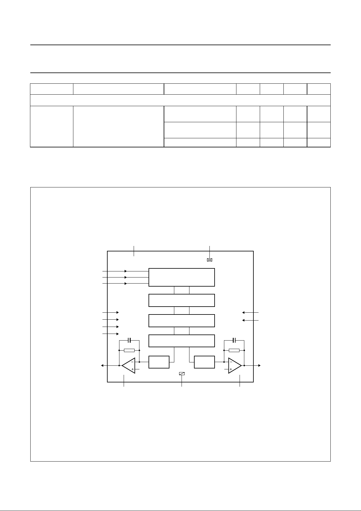
6 BLOCK DIAGRAM
handbook, full pagewidth
BCK
WS
DATAI
V
DDD
4
1
2
3
DIGITAL INTERFACE
V
SSD
5
− 7.0 − mW
− 17 − mW
DE-EMPHASIS
INTERPOLATION FILTER
NOISE SHAPER
DAC
V
SYSCLK
MUTE
DEEM
PCS
VOUTL
UDA1334TS
6
8
9
10
14
13 12
V
DDA
Fig.1 Block diagram.
1999 Nov 11 5
SSA
7
SFOR1
11
SFOR0
V
ref(DAC)
16
VOUTR
MGL877
DAC
15

Philips Semiconductors Preliminary specification
Low power audio DAC UDA1334TS
7 PINNING
SYMBOL PIN PAD TYPE DESCRIPTION
BCK 1 5 V tolerant digital input pad; note 1 bit clock input
WS 2 5 V tolerant digital input pad; note 1 word select input
DATAI 3 5 V tolerant digital input pad; note 1 serial data input
V
DDD
V
SSD
SYSCLK 6 5 V tolerant digital input pad; note 1 system clock input
SFOR1 7 5 V tolerant digital input pad; note 1 serial format select 1
MUTE 8 5 V tolerant digital input pad; note 1 mute control
DEEM 9 5 V tolerant digital input pad; note 1 de-emphasis control
PCS 10 3-level input pad; note 2 power control and sampling frequency select
SFOR0 11 digital input pad; note 2 serial format select 0
V
ref(DAC)
V
DDA
VOUTL 14 analog output pad DAC output left
V
SSA
VOUTR 16 analog output pad DAC output right
4 digital supply pad digital supply voltage
5 digital ground pad digital ground
12 analog pad DAC reference voltage
13 analog supply pad DAC analog supply voltage
15 analog ground pad DAC analog ground
Notes
1. 5 V tolerantis only supportedif the powersupply voltage isbetween 2.7 and 3.6 V. Forlower power supplyvoltages
this is maximum 3.3 V tolerant.
2. Because of test issues these pads are not 5 V tolerant and they should be at power supply voltage level or at a
maximum of 0.5 V above that level.
handbook, halfpage
BCK
WS
DATAI
V
DDD
V
SSD
1
2
3
4
UDA1334TS
5
6
7
8
MGL878
16
15
14
13
12
11
10
9
VOUTR
V
SSA
VOUTL
V
DDA
V
ref(DAC)
SFOR0SYSCLK
PCSSFOR1
DEEMMUTE
Fig.2 Pin configuration.
1999 Nov 11 6
 Loading...