

Philips UDA1325H-N103, UDA1325H-N1, UDA1325PS-N106, UDA1325H-N106 Datasheet
DATA SH EET
Preliminary specification
File under Integrated Circuits, IC01
1999 May 10
INTEGRATED CIRCUITS
UDA1325
Universal Serial Bus (USB) CODEC

1999 May 10 2
Philips Semiconductors Preliminary specification
Universal Serial Bus (USB) CODEC UDA1325
FEATURES
General
• High Quality USB-compliant Audio/HID device
• Supports 12 Mbits/s serial data transmission
• Fully USB Plug and Play operation
• Supports ‘Bus-powered’ and ‘Self-powered’ operation
• 3.3 V power supply
• Low power consumption with optional efficient power
control
• On-chip clock oscillator, only an external crystal is
required.
Audio playback channel
• One isochronous output endpoint
• Supports multiple audio data formats (8, 16 and 24 bits)
• Adaptive sample frequency support from 5 to 55 kHz
• One master 20-bit I2S digital stereo playback output,
I2S and LSB justified serial formats
• One slave 20-bit I2S digital stereo playback input,
I2S and LSB justified serial formats
• Selectable volume control for left and right channel
• Soft mute control
• Digital bass and treble tone control
• Selectable on-chip digital de-emphasis
• Low total harmonic distortion (typical 90 dB)
• High signal-to-noise ratio (typical 95 dB)
• One stereo Line output.
Audio recording channel
• One isochronous input endpoint
• Supports multiple audio data formats (8, 16 and 24 bits)
• Twelve selectable sample rates (4, 8, 16 or 32 kHz;
5.5125, 11.025, 22.05 or 44.1 kHz; 6, 12, 24 or 48 kHz)
via analog PLL (APLL).
• Selectable sample rate between 5 to 55 kHz via a
second oscillator (optional)
• One slave 20-bit I2S digital stereo recording input,
I2S and LSB justified serial formats
• Programmable Gain Amplifier for left and right channel
• Low total harmonic distortion (typical 85 dB)
• High signal-to-noise ratio (typical 90 dB)
• One stereo Line/Microphone input.
USB endpoints
• 2 control endpoints
• 2 interrupt endpoints
• 1 isochronous data sink endpoint
• 1 isochronous data source endpoint.
Document references
•
“USB Specification”
•
“USB Device Class Definition for Audio Devices”
•
“Device Class Definition for Human Interface Devices
(HID)”
•
“USB HID Usage Table”
.
•
“USB Common Class Specification”
.

1999 May 10 3
Philips Semiconductors Preliminary specification
Universal Serial Bus (USB) CODEC UDA1325
APPLICATIONS
• USB monitors
• USB speakers
• USB microphones
• USB headsets
• USB telephone/answering machines
• USB links in consumer audio devices.
GENERAL DESCRIPTION
The UDA1325 is a single chip stereo USB codec
incorporating bitstream converters designed for
implementation in USB-compliant audio peripherals and
multimedia audio applications. It contains a USB interface,
an embedded microcontroller, an Analog-to-Digital
Interface (ADIF) and an Asynchronous Digital-to-Analog
Converter (ADAC).
The USB interface consists of an analog front-end and a
USB processor. The analog front-end transforms the
differential USB data into a digital data stream. The USB
processor buffers the incoming and outgoing data from the
analog front-end and handles all low-level USB protocols.
The USB processor selects the relevant data from the
universal serial bus, performs an extensive error detection
and separates control information and audio information.
The control information is made accessible to the
microcontroller. At playback, the audio information
becomes available at the digital I
2
S output of the digital I/O
module or is fed directly to the ADAC. At recording, the
audio information is delivered by the ADIF or by the digital
I2S input of the I2S-bus interface.
All I2S inputs and I2S outputs support standard I2S-bus
format and the LSB justified serial data format with word
lengths of 16, 18 and 20 bits.
Via the digital I/O module with its I2S input and output, an
external DSP can be used for adding extra sound
processing features for the audio playback channel.
The microcontroller is responsible for handling the
high-level USB protocols, translating the incoming control
requests and managing the user interface via general
purpose pins and an I2C-bus.
The ADAC enables the wide and continuous range of
playback sampling frequencies. By means of a Sample
Frequency Generator (SFG), the ADAC is able to
reconstruct the average sample frequency from the
incoming audio samples. The ADAC also performs the
playback sound processing. The ADAC consists of a
FIFO, an unique audio feature processing DSP, the SFG,
digital filters, a variable hold register, a Noise Shaper (NS)
and a Filter Stream DAC (FSDAC) with line output drivers.
The audio information is applied to the ADAC via the USB
processor or via the digital I2S input of the digital I/O
module.
The ADIF consists of an Programmable Gain Amplifier
(PGA), an Analog-to-Digital Converter (ADC) and a
Decimator Filter (DF). An Analog Phase Lock Loop (APLL)
or oscillator is used for creating the clock signal of the
ADIF. The clock frequency for the ADIF can be controlled
via the microcontroller. Several clock frequencies are
possible for sampling the analog input signal at different
sampling rates.
The wide dynamic range of the bitstream conversion
technique used in the UDA1325 for both the playback and
recording channel guarantees a high audio sound quality.
ORDERING INFORMATION
TYPE NUMBER
PACKAGE
NAME DESCRIPTION VERSION
UDA1325PS SDIP42 plastic shrink dual in-line package; 42 leads (600 mil) SOT270-1
UDA1325H QFP64 plastic quad flat package; 64 leads (lead length 1.95 mm);
body 14 × 20 × 2.8 mm
SOT319-2
1999 May 10 4
Philips Semiconductors Preliminary specification
Universal Serial Bus (USB) CODEC UDA1325
QUICK REFERENCE DATA
Note
1. Exclusive the IDDE current which depends on the components connected to the I/O pins.
SYMBOL PARAMETER CONDITIONS MIN. TYP. MAX. UNIT
Supplies
V
DDE
supply voltage periphery 4.75 5.0 5.25 V
V
DDI
supply voltage core 3.0 3.3 3.6 V
I
DD(tot)
total supply current − 60 tbf mA
I
DD(tot)(ps)
total supply current in power-saving
mode
note 1 − 360 −µA
Dynamic performance DAC
(THD + N)/S total harmonic distortion plus
noise-to-signal ratio
f
s
= 44.1 kHz; RL=5kΩ
f
i
= 1 kHz (0 dB) −−90 −80 dB
− 0.0032 0.01 %
f
i
= 1 kHz (−60 dB) −−30 −20 dB
− 3.2 10 %
S/N signal-to-noise ratio at bipolar zero A-weighted at code 0000H 90 95 − dBA
V
o(FS)(rms)
full-scale output voltage
(RMS value)
VDD= 3.3 V − 0.66 − V
Dynamic performance PGA and ADC
(THD + N)/S total harmonic distortion plus
noise-to-signal ratio
f
s
= 44.1 kHz;
PGA gain = 0 dB
f
i
= 1 kHz; (0 dB);
Vi= 1.0 V (RMS)
−−85 −80 dB
− 0.0056 0.01 %
f
i
= 1 kHz (−60 dB) −−30 −20 dB
− 3.2 10.0 %
S/N signal-to-noise ratio V
i
= 0.0 V 90 95 − dBA
General characteristics
f
i(s)
audio input sample frequency 5 − 55 kHz
T
amb
operating ambient temperature 0 25 70 °C

1999 May 10 5
Philips Semiconductors Preliminary specification
Universal Serial Bus (USB) CODEC UDA1325
BLOCK DIAGRAM
Fig.1 Block diagram (QFP64 package).
handbook, full pagewidth
MGM108
TIMING
ANALOG
PLL
OSC
48 MHz
OSC
ADC
24 (19)
27
25 (20)
26 (21)
28 (22)
52 (39)
53 (40)
54 (41)
55 (42)
63 (4)
1 (5)
2 (6)
13 (14)
17 (16)
15 (15)
(12) 11
(13) 12
(10) 9
(11) 10
(23) 32
(24) 33
(29) 38
(30) 39
(33) 42
(35) 44
ANALOG FRONT-END
USB-PROCESSOR
DIGITAL I/O
FIFO
AUDIO FEATURE
PROCESSING DSP
UPSAMPLE FILTERS
VARIABLE HOLD REGISTER
3rd-ORDER NOISE SHAPER
REFERENCE VOLTAGE
57 (1)
59 (2)
61 (3)
43 (34)
47 (36)
8 (9) 6 (8)
MICRO-
CONTROLLER
TEST
CONTROL
BLOCK
SAMPLE
FREQUENCY
GENERATOR
MUX
I2S-BUS
INTERFACE
DECIMATOR
FILTER
PGA
LEFT
Σ∆ ADC
PGA
RIGHT
Σ∆ ADC
LEFT
DAC
RIGHT
DAC
49 (37)
51 (38)
45, 46 41 (32) 40 (31)
V
ref(AD)
V
ref(DA)
(28) 37
(25) 34
(27) 36
(26) 35
(7) 4
(18) 21
(17) 19
n.c.
UDA1325
+
−
−
+
VRN
VINR
V
SSA2
VINL
V
SSA1
V
DDA1
VOUTR
RTCB
GP4/BCKO
SHTCB
D−
7, 5, 3, 64,
62, 60, 58, 56
P0.7 to P0.0
14, 16, 18, 20,
22, 23, 29, 30
P2.0 to P2.7
D+
V
DDI
V
SSI
V
DDE
GP1/DI
GP0/BCKI
V
DDA2
BCK
48
EA
50
ALE
WS
DA
31
PSEN
V
SSA3
XTAL2a
V
DDA3
VRP
GP2/DO
GP3/WSO
XTAL1a
SDA
V
SSX
XTAL1b
XTAL2b
CLK
V
DDX
V
SSO
VOUTL
TC
SCL
V
DDO
V
SSE
GP5/WSI
The pin numbers given in parenthesis refer to the SDIP42 version.
1999 May 10 6
Philips Semiconductors Preliminary specification
Universal Serial Bus (USB) CODEC UDA1325
PINNING
SYMBOL
PIN
QFP64
PIN
SDIP42
I/O DESCRIPTION
GP3/WSO 1 5 I/O general purpose pin 3 or word select output
GP4/BCKO 2 6 I/O general purpose pin 4 or bit clock output
P0.5 3 − I/O Port 0.5 of the microcontroller
SHTCB 4 7 I shift clock of the test control block (active HIGH)
P0.6 5 − I/O Port 0.6 of the microcontroller
D− 6 8 I/O negative data line of the differential data bus, conforms to the USB
standard
P0.7 7 − I/O Port 0.7 of the microcontroller
D+ 8 9 I/O positive data line of the differential data bus, conforms to the USB
standard
V
DDI
910−digital supply voltage for core
V
SSI
10 11 − digital ground for core
V
SSE
11 12 − digital ground for I/O pads
V
DDE
12 13 − digital supply voltage for I/O pads
GP1/DI 13 14 I/O general purpose pin 1 or data input
P2.0 14 − I/O Port 2.0 of the microcontroller
GP5/WSI 15 15 I/O general purpose pin 5 or word select input
P2.1 16 − I/O Port 2.1 of the microcontroller
GP0/BCKI 17 16 I/O general purpose pin 0 or bit clock input
P2.2 18 − I/O Port 2.2 of the microcontroller
SCL 19 17 I/O serial clock line I
2
C-bus
P2.3 20 − I/O Port 2.3 of the microcontroller
SDA 21 18 I/O serial data line I
2
C-bus
P2.4 22 − I/O Port 2.4 of the microcontroller
P2.5 23 − I/O Port 2.5 of the microcontroller
V
SSX
24 19 − crystal oscillator ground (48 MHz)
XTAL1b 25 20 I crystal input (analog; 48 MHz)
XTAL2b 26 21 O crystal output (analog; 48 MHz)
CLK 27 − O 48 MHz clock output signal
V
DDX
28 22 − supply crystal oscillator (48 MHz)
P2.6 29 − I/O Port 2.6 of the microcontroller
P2.7 30 − I/O Port 2.7 of the microcontroller
PSEN 31 − I/O program store enable (active LOW)
V
DDO
32 23 − supply voltage for operational amplifier
V
SSO
33 24 − operational amplifier ground
VOUTL 34 25 O voltage output left channel
TC 35 26 I test control input (active HIGH)
RTCB 36 27 I asynchronous reset input of the test control block (active HIGH)
VOUTR 37 28 O voltage output right channel
1999 May 10 7
Philips Semiconductors Preliminary specification
Universal Serial Bus (USB) CODEC UDA1325
V
DDA1
38 29 − analog supply voltage 1
V
SSA1
39 30 − analog ground 1
V
ref(DA)
40 31 O reference voltage output DAC
V
ref(AD)
41 32 O reference voltage output ADC
V
DDA2
42 33 − analog supply voltage 2
VINL 43 34 I input signal left channel PGA
V
SSA2
44 35 − analog ground 2
n.c. 45 −−not connected
n.c. 46 −−not connected
VINR 47 36 I input signal right channel PGA
EA 48 −−external access (active LOW)
VRN 49 37 I negative reference input voltage ADC
ALE 50 −−address latch enable (active HIGH)
VRP 51 38 I positive reference input voltage ADC
V
DDA3
52 39 − supply voltage for crystal oscillator and analog PLL
XTAL2a 53 40 O crystal output (analog; ADC)
XTAL1a 54 41 I crystal input (analog; ADC)
V
SSA3
55 42 − crystal oscillator and analog PLL ground
P0.0 56 − I/O Port 0.0 of the microcontroller
DA 57 1 I data Input (digital)
P0.1 58 − I/O Port 0.1 of the microcontroller
WS 59 2 I word select Input (digital)
P0.2 60 − I/O Port 0.2 of the microcontroller
BCK 61 3 I bit clock Input (digital)
P0.3 62 − I/O Port 0.3 of the microcontroller
GP2/DO 63 4 I/O general purpose pin 2 or data output
P0.4 64 − I/O Port 0.4 of the microcontroller
SYMBOL
PIN
QFP64
PIN
SDIP42
I/O DESCRIPTION
1999 May 10 8
Philips Semiconductors Preliminary specification
Universal Serial Bus (USB) CODEC UDA1325
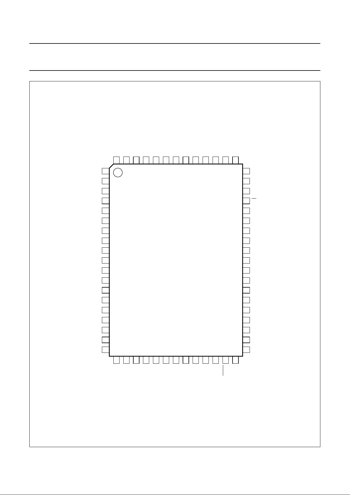
Fig.2 Pin configuration (QFP64 package).
handbook, full pagewidth
UDA1325H
MGL349
1
2
3
4
5
6
7
8
9
10
11
12
13
14
15
16
17
18
19
GP3/WSO
GP4/BCKO
P0.5
SHTCB
P0.6
D−
P0.7
D+
V
DDI
V
SSI
V
SSE
V
DDE
GP1/DI
P2.0
GP5/WSI
P2.1
GP0/BCKI
P2.2
SCL
VRP
ALE
VRN
EA
VINR
n.c.
n.c.
V
SSA2
VINL
V
DDA2
V
ref(AD)
V
ref(DA)
V
SSA1
V
DDA1
VOUTR
RTCB
TC
VOUTL
V
SSO
51
50
49
48
47
46
45
44
43
42
41
40
39
38
37
36
35
34
33
20
21
22
23
24
25
26
27
28
29
30
31
32
64
63
62
61
60
59
58
57
56
55
54
53
52
P0.4
GP2/DO
P0.3
BCK
P0.2WSP0.1DAP0.0
V
SSA3
XTAL1a
XTAL2a
V
DDA3
P2.3
SDA
P2.4
P2.5
V
SSX
XTAL1b
XTAL2b
CLK
V
DDX
P2.6
P2.7
PSEN
V
DDO

1999 May 10 9
Philips Semiconductors Preliminary specification
Universal Serial Bus (USB) CODEC UDA1325
Fig.3 Pin configuration (SDIP42 package).
handbook, halfpage
UDA1325
MGM106
1
2
42
41
3
4
5
6
7
8
9
10
11
12
13
14
15
16
17
18
19
20
40
39
38
37
36
35
34
33
32
31
30
29
28
27
26
25
24
23
2221
V
SSA3
XTAL1a
XTAL2a
V
DDA3
VRP
VRN
VINR
V
SSA2
VINL
V
DDA2
V
ref(AD)
V
ref(DA)
V
SSA1
V
DDA1
VOUTR
RTCB
TC
VOUTL
V
SSO
V
DDO
V
DDX
DA
WS
BCK
GP2/DO
GP3/WSO
GP4/BCKO
SHTCB
D−
D+
V
DDI
V
SSI
V
SSE
V
DDE
GP1/DI
GP5/WSI
GP0/BCKI
SCL
SDA
V
SSX
XTAL1b
XTAL2b
FUNCTIONAL DESCRIPTION
The Universal Serial Bus (USB)
Data and power is transferred via the USB over a 4-wire
cable. The signalling occurs over two wires and
point-to-point segments. The signals on each segment are
differentially driven into a cable of 90 Ω intrinsic
impedance. The differential receiver features input
sensitivity of at least 200 mV and sufficient common mode
rejection.
The analog front-end
The analog front-end is an on-chip generic USB
transceiver. It is designed to allow voltage levels up to V
DD
from standard or programmable logic to interface with the
physical layer of the USB. It is capable of receiving and
transmitting serial data at full speed (12 Mbits/s).
The USB processor
The USB processor forms the interface between the
analog front-end, the ADIF, the ADAC and the
microcontroller. The USB processor consists of:
• A bit clock recovery circuit
• The Philips Serial Interface Engine (PSIE)
• The Memory Management Unit (MMU)
• The Audio Sample Redistribution (ASR) module.
Bit clock recovery
The bit clock recovery circuit recovers the clock from the
incoming USB data stream using four times over-sampling
principle. It is able to track jitter and frequency drift
specified by the USB specification.
Philips Serial Interface Engine (PSIE)
The Philips SIE implements the full USB protocol layer.
It translates the electrical USB signals into data bytes and
control signals. Depending upon the USB device address
and the USB endpoint address, the USB data is directed
to the correct endpoint buffer. The data transfer could be
of bulk, isochronous, control or interrupt type.
The functions of the PSIE include: synchronization pattern
recognition, parallel/serial conversion, bit
stuffing/de-stuffing, CRC checking/generation, PID
verification/generation, address recognition and
handshake evaluation/generation.
The amount of bytes/packet on all endpoints is limited by
the PSIE hardware to 8 bytes/packet, except for both
isochronous endpoints (336 bytes/packet).

1999 May 10 10
Philips Semiconductors Preliminary specification
Universal Serial Bus (USB) CODEC UDA1325
Memory Management Unit (MMU) and integrated RAM
The MMU and integrated RAM handle the temporary data
storage of all USB packets that are received or sent over
the bus.
The MMU and integrated RAM handle the differences
between data rate of the USB and the application allowing
the microcontroller to read and write USB packets at its
own speed.
The audio data is transferred via an isochronous data sink
endpoint or source endpoint and is stored directly into the
RAM. Consequently, no handshaking mechanism is used.
Audio Sample Redistribution (ASR)
The ASR reads the audio samples from the MMU and
integrated RAM and distributes these samples equidistant
over a 1 ms frame period. The distributed audio samples
are translated by the digital I/O module to standard I
2
S-bus
format or 16, 18 or 20 bits LSB-justified I2S-bus format.
The ASR generates the bit clock output (BCKO) and the
Word Select Output signal (WSO) of the I2S output.
The 80C51 microcontroller
The microcontroller receives the control information
selected from the USB by the USB processor. It can be
used for handling the high-level USB protocols and the
user interfaces. The microcontroller does not handle the
audio stream.
The major task of the software process that is mapped
upon the microcontroller, is to control the different modules
of the UDA1325 in such a way that it behaves as a USB
device.
The embedded 80C51 microcontroller is compatible with
the 80C51 family of microcontrollers described in the
80C51 family single-chip 8-bit microcontrollers of “Data
Handbook IC20”, which should be read in conjunction with
this data sheet.
The internal ROM size is 12 kbyte. The internal RAM size
is 256 byte. A Watchdog Timer is not integrated.
The Analog-to-Digital Interface (ADIF)
The ADIF is used for sampling an analog input signal from
a microphone or line input and sending the audio samples
to the USB interface. The ADIF consists of a stereo
Programmable Gain Amplifier (PGA), a stereo
Analog-to-Digital Converter (ADC) and Decimation Filters
(DFs). The sample frequency of the ADC is determined by
the ADC clock (see Section “The clock source of the
analog-to-digital interface”). The user can also select a
digital serial input instead of an analog input. In this event
the sample frequency is determined by the continuous WS
clock with a range between 5 to 55 kHz. Digital serial input
is possible with four formats (I
2
S-bus, 16, 18 or 20 bits
LSB-justified).
Programmable Gain Amplifier circuit (PGA)
This circuit can be used for a microphone or line input.
The input audio signals can be amplified by seven different
gains (−3 dB, 0 dB, 3 dB, 9 dB, 15 dB, 21 dB and 27 dB).
The gain settings are given in Table 17.
The Analog-to-Digital Converter (ADC)
The stereo ADC of the UDA1325 consists of two 3rd-order
Sigma-Delta modulators. They have a modified
Ritchie-coder architecture in a differential switched
capacitor implementation. The oversampling ratio is 128.
Both ADCs can be switched off in power saving mode (left
and right separate). The ADC clock is generated by the
analog PLL or the ADC oscillator.
The Decimation Filter (DF)
The decimator filter converts the audio data from 128f
s
down to 1fs with a word width of 8, 16 or 24 bits. This data
can be transmitted over the USB as mono or stereo in
1, 2 or 3 bytes/sample. The decimator filters are clocked
by the ADC clock.
1999 May 10 11
Philips Semiconductors Preliminary specification
Universal Serial Bus (USB) CODEC UDA1325
The clock source of the analog-to-digital interface
The clock source of the ADIF is the analog PLL or the ADC oscillator. The preferred clock source can be selected.
The ADC clock used for the ADC and decimation filters is obtained by dividing the clock signal coming from the analog
PLL or from the ADC oscillator by a factor Q.
Using the analog PLL the user can select 3 basic APLL clock frequencies (see Table 1).
By connecting the appropriate crystal the user can choose any clock signal between 8.192 and 14.08 MHz via the ADC
oscillator.
Table 1 The analog PLL clock output frequencies
The dividing factor Q can be selected via the microcontroller. With this dividing factor Q the user can select a range of
ADC clock signals allowing several different sample frequencies (see Table 2).
Table 2 ADC clock frequencies and sample frequencies based upon using the APLL as a clock source
Table 3 ADC clock frequencies and sample frequencies based upon using the OSCAD as a clock source
Notes
1. The oscillator frequency (and therefore the crystal) of OSCAD must be between 8.192 and 14.08 MHz.
2. The Q factor can be 1, 2, 4 or 8.
3. Sample frequencies below 5 kHz and above 55 kHz are not supported.
FCODE (1 AND 0)
APLL CLOCK
FREQUENCY (MHz)
00 11.2896
01 8.1920
10 12.2880
11 11.2896
APLL CLOCK
FREQUENCY (MHz)
DIVIDE FACTOR Q ADC CLOCK FREQUENCY (MHz) SAMPLE FREQUENCY (kHz)
8.1920 1 4.096 32
2 2.048 16
4 1.024 8
8 0.512 (not supported) 4 (not supported)
11.2896 1 5.6448 44.1
2 2.8224 22.05
4 1.4112 11.025
8 0.7056 5.5125
12.2880 1 6.144 48
2 3.072 24
4 1.536 12
8 0.768 6
OSCAD CLOCK
FREQUENCY (MHz)
DIVIDE FACTOR Q ADC CLOCK FREQUENCY (MHz) SAMPLE FREQUENCY (kHz)
f
osc
(1)
Q
(2)
f
osc
/(2Q) f
osc
/(256Q)
(3)

1999 May 10 12
Philips Semiconductors Preliminary specification
Universal Serial Bus (USB) CODEC UDA1325
The Asynchronous Digital-to-Analog Converter
(ADAC)
The ADAC receives audio data from the USB processor or
from the digital I/O-bus. The ADAC is able to reconstruct
the sample clock from the rate at which the audio samples
arrive and handles the audio sound processing. After the
processing, the audio signal is upsampled, noise-shaped
and converted to analog output voltages capable of driving
a line output.
The ADAC consists of:
• A Sample Frequency Generator (SFG)
• FIFO registers
• An audio feature processing DSP
• Two digital upsampling filters and a variable hold
register
• A digital Noise Shaper (NS)
• A Filter Stream DAC (FSDAC) with integrated filter and
line output drivers.
The Sample Frequency Generator (SFG)
The SFG controls the timing signals for the asynchronous
digital-to-analog conversion. By means of a digital PLL,
the SFG automatically recovers the applied sampling
frequency and generates the accurate timing signals for
the audio feature processing DSP and the upsampling
filters.
The lock time of the digital PLL can be chosen (see
Table 8). While the digital PLL is not in lock, the ADAC is
muted. As soon as the digital PLL is in lock, the mute is
released as described in Section “Soft mute control”.
First-In First-Out (FIFO) registers
The FIFO registers are used to store the audio samples
temporarily coming from the USB processor or from the
digital I/O input. The use of a FIFO (in conjunction with the
SFG) is necessary to remove all jitter present on the
incoming audio signal.
The sound processing DSP
A DSP processes the sound features. The control and
mapping of the sound features is explained in Section
“Controlling the playback features of the ADAC”.
Depending on the sampling rate (f
s
) the DSP knows four
frequency domains in which the treble and bass are
regulated. The domain is chosen automatically.
Table 4 Frequency domains for audio processing by the
DSP
The upsampling filters and variable hold function
After the audio feature processing DSP two upsampling
filters and a variable hold function increase the
oversampling rate to 128f
s
.
The noise shaper
A 3rd-order noise shaper converts the oversampled data
to a noise-shaped bitstream for the FSDAC. The in-band
quantization noise is shifted to frequencies well above the
audio band.
The Filter Stream DAC (FSDAC)
The FSDAC is a semi-digital reconstruction filter that
converts the 1-bit data stream of the noise shaper to an
analog output voltage. The filter coefficients are
implemented as current sources and are summed at
virtual ground of the output operational amplifier. In this
way very high signal-to-noise performance and low clock
jitter sensitivity is achieved. A post filter is not needed
because of the inherent filter function of the DAC.
On-board amplifiers convert the FSDAC output current to
an output voltage signal capable of driving a line output.
DOMAIN SAMPLE FREQUENCY (kHz)
1 5to12
212to25
325to40
440to55

1999 May 10 13
Philips Semiconductors Preliminary specification
Universal Serial Bus (USB) CODEC UDA1325
USB ENDPOINT DESCRIPTION
The UDA1325 has following six endpoints:
• USB control endpoint 0
• USB control endpoint 1
• USB status interrupt endpoint 1
• USB status interrupt endpoint 2
• Isochronous data sink endpoint
• Isochronous data source endpoint.
Table 5 Endpoint description
CONTROLLING THE PLAYBACK FEATURES
Controlling the playback features of the ADAC
The exchange of control information between the microcontroller and the ADAC is accomplished through a serial
hardware interface comprising the following pins:
L3_DATA: microcontroller interface data line
L3_MODE: microcontroller interface mode line
L3_CLK: microcontroller interface clock line.
See also the description of Port 3 of the 80C51 microcontroller.
Information transfer through the microcontroller bus is organized in accordance with the so-called ‘L3’ format, in which
two different modes of operation can be distinguished; address mode and data transfer mode.
The address mode is required to select a device communicating via the L3-bus and to define the destination registers
for the data transfer mode. Data transfer for the UDA1325 can only be in one direction, from microcontroller to ADAC to
program its sound processing features and other functional features.
A
DDRESS MODE
The address mode is used to select a device (in this case the ADAC) for subsequent data transfer and to define the
destination registers. The address mode is characterized by L3_MODE being LOW and a burst of 8 pulses on L3_CLK,
accompanied by 8 data bits on L3_DATA. Data bits 0 and 1 indicate the type of the subsequent data transfer as shown
in Table 6.
ENDPOINT
NUMBER
ENDPOINT
INDEX
ENDPOINT TYPE DIRECTION
MAX. PACKET
SIZE (BYTES)
0 0 control (default) out 8
1in8
1 2 control out 8
3in8
2 4 interrupt in 8
3 5 interrupt in 8
4 6 isochronous out out 336
5 7 isochronous in in 336

1999 May 10 14
Philips Semiconductors Preliminary specification
Universal Serial Bus (USB) CODEC UDA1325
Table 6 Selection of data transfer type
Data bits 7 to 2 represent a 6-bit device address, with bit 7 being the MSB and bit 2 the LSB. The address of the ADAC
is 000101 (bits 7 to 2). In the event that the ADAC receives a different address, it will deselect its microcontroller interface
logic.
D
AT A TRANSFER MODE
The selection preformed in the address mode remains active during subsequent data transfers, until the ADAC receives
a new address command. The data transfer mode is characterized by L3_MODE being HIGH and a burst of 8 pulses on
L3_CLK, accompanied by 8 data bits. All transfers are bitwise, i.e. they are based on groups of 8 bits. Data will be stored
in the ADAC after the eight bit of a byte has been received. The principle of a multibyte transfer is illustrated in the figure
below.
P
ROGRAMMING THE SOUND PROCESSING AND OTHER FEATURES
The sound processing and other feature values are stored in independent registers. The first selection of the registers is
achieved by the choice of data transfer type. This is performed in the address mode, bits 1 and 0 (see Table 6).
The second selection is performed by bit 7 and/or bit 6 of the data byte depending of the selected data transfer type.
Data transfer type ‘audio feature registers’
When the data transfer type ‘audio feature registers’ is selected 4 audio feature registers can be selected depending on
bits 7 and 6 of the data byte (see Table 7).
BIT1 BIT0 DATA TRANSFER TYPE
0 0 audio feature registers (volume left, volume right, bass and treble)
0 1 not used
1 0 control registers
1 1 not used
dbook, full pagewidth
t
halt
address
L3DATA
L3CLOCK
L3MODE
addressdata byte #1 data byte #2
MGD018

1999 May 10 15
Philips Semiconductors Preliminary specification
Universal Serial Bus (USB) CODEC UDA1325
Table 7 ADAC audio feature registers
The sequence for controlling the ADAC audio feature registers via the L3-bus is given in the figure below.
Data transfer type ‘control registers’
When the data transfer type ‘control registers’ is selected 2 general control registers can be selected depending on bit 7
of the data byte (see Table 7).
The sequence for controlling the ADAC control registers via the L3-bus is given in the figure below.
BIT7 BIT6 BIT5 BIT4 BIT3 BIT2 BIT1 BIT0 REGISTER
0 0 VR5 VR4 VR3 VR2 VR1 VR0 volume right
0 1 VL5 VL4 VL3 VL2 VL1 VL0 volume left
1 0 X BB4 BB3 BB2 BB1 BB0 bass
1 1 X TR4 TR3 TR2 TR1 TR0 treble
book, full pagewidth
MGS270
0
bit 0
DATA_TRANSFER_TYPE
L3_DATA
(L3_MODE = LOW)
0 1 0 1
DEVICE ADDRESS = $5
0 0 0
bit 7
X
bit 0
L3_DATA
(L3_MODE = HIGH)
X X X X
REGISTER
ADDRESS
LEFT VOLUME; TREBLE
RIGHT VOLUME; BASS
X
X X
bit 7
L3_CLK
book, full pagewidth
MGS269
0
bit 0
DATA_TRANSFER_TYPE
L3_DATA
(L3_MODE = LOW)
1 1 0 1
DEVICE ADDRESS = $5
0 0 0
bit 7
X
bit 0
L3_DATA
(L3_MODE = HIGH)
X X X X
REGISTER
ADDRESSDATA OF THE CONTROL REGISTER
X
X X
bit 7
L3_CLK
1999 May 10 16
Philips Semiconductors Preliminary specification
Universal Serial Bus (USB) CODEC UDA1325
Table 8 ADAC general control registers
Soft mute control
When the mute (bit 1 of control register 0) is active for the playback channel, the value of the sample is decreased
smoothly to zero following a raised cosine curve. There are 32 coefficients used to step down the value of the data, each
one being used 32 times before stepping to the next. This amounts to a mute transition of 23 ms at f
s
= 44.1 kHz. When
the mute is released, the samples are returned to the full level again following a raised cosine curve with the same
coefficients being used in reversed order.
The mute, on the master channel is synchronized to the sample clock, so that operation always takes place on complete
samples.
REGISTER BIT DESCRIPTION V ALUE COMMENT
Control register 0 0 reset ADAC 0 = not reset
1 = reset
1 soft mute control 0 = not muted
1 = mutes
2 synchronous/asynchronous 0 = asynchronous
1 = synchronous
select 0
3 channel manipulation 0 = L -> L, R -> R
1=L->R, R->L
4 de-emphasis 0 = de-emphasis off
1 = de-emphasis on
6 and 5 audio mode 00 = flat mode
01 = min. mode
10 = min. mode
11 = max. mode
7 selecting bit 0
Control register 1 1 and 0 serial I
2
S-bus input format 00 = I2S-bus
01 = 16-bit LSB justified
10 = 18-bit LSB justified
11 = 20-bit LSB justified
3 and 2 digital PLL mode 00 = adaptive
01 = fix state 1
10 = fix state 2
11 = fix state 3
select 00
4 digital PLL lock mode 0 = adaptive
1 = fixed
select 1
6 and 5 digital PLL lock speed 00 = lock after 512 samples
01 = lock after 2048 samples
10 = lock after 4096 samples
11 = lock after 16348 samples
select 00
7 selecting bit 1
 Loading...