

Philips UDA1324TS-N1 Datasheet
DATA SH EET
Preliminary specification
Supersedes data of 1999 Oct 12
File under Integrated Circuits, IC01
2000 Jan 20
INTEGRATED CIRCUITS
UDA1324TS
Ultra low-voltage stereo filter DAC
2000 Jan 20 2
Philips Semiconductors Preliminary specification
Ultra low-voltage stereo filter DAC UDA1324TS
FEATURES
General
• Low power consumption
• Ultra low power supply voltage from 1.9 to 2.7 V
• Selectable controlvia L3 microcontroller interface or via
static pin control
• System clock frequencies of 256fs, 384fsand 512f
s
selectable via L3 interface or 256fsand 384fs via static
pin control
• Supports sampling frequencies (fs) from 16 to 48 kHz
• Integrated digital filter plus non inverting
Digital-to-Analog Converter (DAC)
• No analog post filtering required for DAC
• Slave mode only applications
• Easy application
• Small package size (SSOP16).
Multiple format input interface
• L3 mode: I2S-bus, MSB-justified or LSB-justified
16, 18 and 20 bits format compatible
• Static pin mode: I2S-bus or LSB-justified
16, 18 and 20 bits format compatible
• 1fs input format data rate.
DAC digital sound processing
• Digital logarithmic volume control in L3 mode
• Digital de-emphasis selection for 32, 44.1 and 48 kHz
sampling frequencies in L3 mode or 44.1 kHz sampling
frequency in static pin mode
• Soft mute control in static pin mode or in L3 mode.
Advanced audio configuration
• Stereo line output (volume control in L3 mode)
• High linearity, wide dynamic range and low distortion.
APPLICATIONS
• Portable digital audio equipment.
GENERAL DESCRIPTION
The UDA1324TS is a single-chip stereo DAC employing
bitstream conversion techniques. The ultra low-voltage
requirements make the device eminently suitable for use
in portable digital audio equipment which incorporates
playback functions.
The UDA1324TS supports the I2S-bus data format with
wordlengths of upto20 bits, the MSB-justified dataformat
with word lengths of up to 20 bits and the LSB-justified
serial data format with word lengths of 16, 18 and 20 bits.
The UDA1324TS can be used in two modes: L3 mode or
static pin mode.
In the L3 mode, all digital sound processing features must
becontrolled via the L3 interface, includingtheselectionof
the system clock setting.
In the two static modes, the UDA1324TS can be operated
in the 256fs and 384fs system clock mode. Muting,
de-emphasis for 44.1 kHz and four digital input formats
(I2S-bus or LSB-justified 16, 18 and 20 bits) can be
selectedvia static pins.TheL3 interface cannot beusedin
this application mode, so volume control is not available in
this mode.
ORDERING INFORMATION
TYPE
NUMBER
PACKAGE
NAME DESCRIPTION VERSION
UDA1324TS SSOP16 plastic shrink small outline package; 16 leads; body width 4.4 mm SOT369-1
2000 Jan 20 3
Philips Semiconductors Preliminary specification
Ultra low-voltage stereo filter DAC UDA1324TS
QUICK REFERENCE DATA
Notes
1. The analog performance figures are measured at 2.0 V supply voltage.
2. The DAC output voltage scales linearly with the power supply voltage.
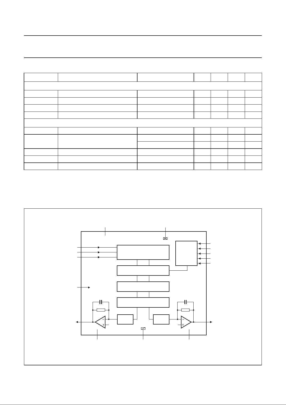
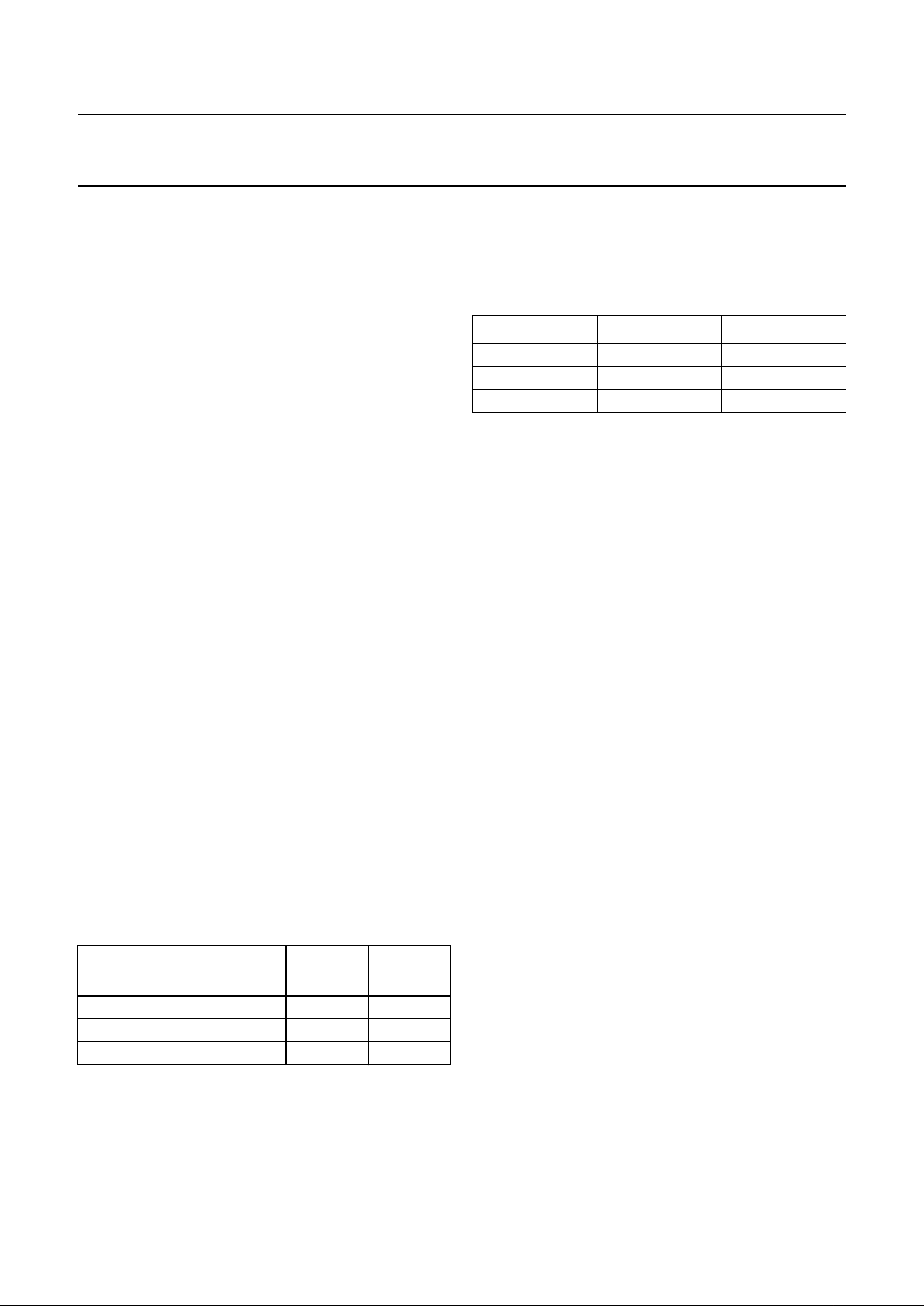
BLOCK DIAGRAM
SYMBOL PARAMETER CONDITIONS MIN. TYP. MAX. UNIT
Supplies
V
DDA
analog supply voltage 1.9 2.0 2.7 V
V
DDD
digital supply voltage 1.9 2.0 2.7 V
I
DDA
analog supply current V
DDA
= 2.0 V − 3.0 − mA
I
DDD
digital supply current V
DDD
= 2.0 V − 1.5 − mA
DAC; note 1
V
o(rms)
output voltage (RMS value) note 2 − 500 − mV
(THD + N)/S total harmonic distortion-plus-noise to
signal ratio
at 0 dB −−83 −78 dB
at −60 dB; A-weighted −−36 − dB
S/N signal-to-noise ratio code = 0; A-weighted − 97 − dB
α
cs
channel separation − 100 − dB
T
amb
ambient temperature −40 − +70
°
C
Fig.1 Block diagram.
handbook, full pagewidth
MBK770
DAC
UDA1324TS
NOISE SHAPER
INTERPOLATION FILTER
VOLUME/MUTE/DE-EMPHASIS
CONTROL
INTERFACE
14
15
DAC
6
DIGITAL INTERFACE
8
16
9
10
3
2
1
4
5
11
7
13 12
VOUTR
BCK
V
SSA
WS
VOUTL
DATAI
V
DDA
V
DDD
V
ref(DAC)
V
SSD
APPL0
SYSCLK
APPL1
APPSEL
APPL2
APPL3
2000 Jan 20 4
Philips Semiconductors Preliminary specification
Ultra low-voltage stereo filter DAC UDA1324TS
PINNING FUNCTIONAL DESCRIPTION
System clock
The UDA1324TS operates in the slave mode only.
Therefore, in all applications the system devices must
provide the system clock. The system frequency (f
sys
) is
selectable and depends on the application mode.
The options are: 256fs, 384fsand 512fs for the L3 mode
and 256fs or 384fs for the static pin mode. The system
clock must be locked in frequency to the digital interface
input signals.
The UDA1324TS supports sampling frequencies (fs) from
16 to 48 kHz.
Application modes
The application mode can be set with the three-level
pin APPSEL (see Table 1):
• L3 mode
• Static pin mode with f
sys
= 384f
s
• Static pin mode with f
sys
= 256fs.
Table 1 Selecting application mode and system clock
frequency via pin APPSEL
The function of an application input pin (active HIGH)
depends on the application mode (see Table 2).
Table 2 Functions of application input pins
For example, in the static pin mode the output signal can
be soft muted by setting pin APPL0 to HIGH.
De-emphasis can be switched on for 44.1 kHz by setting
pin APPL1to HIGH; setting pin APPL1to LOW will disable
de-emphasis.
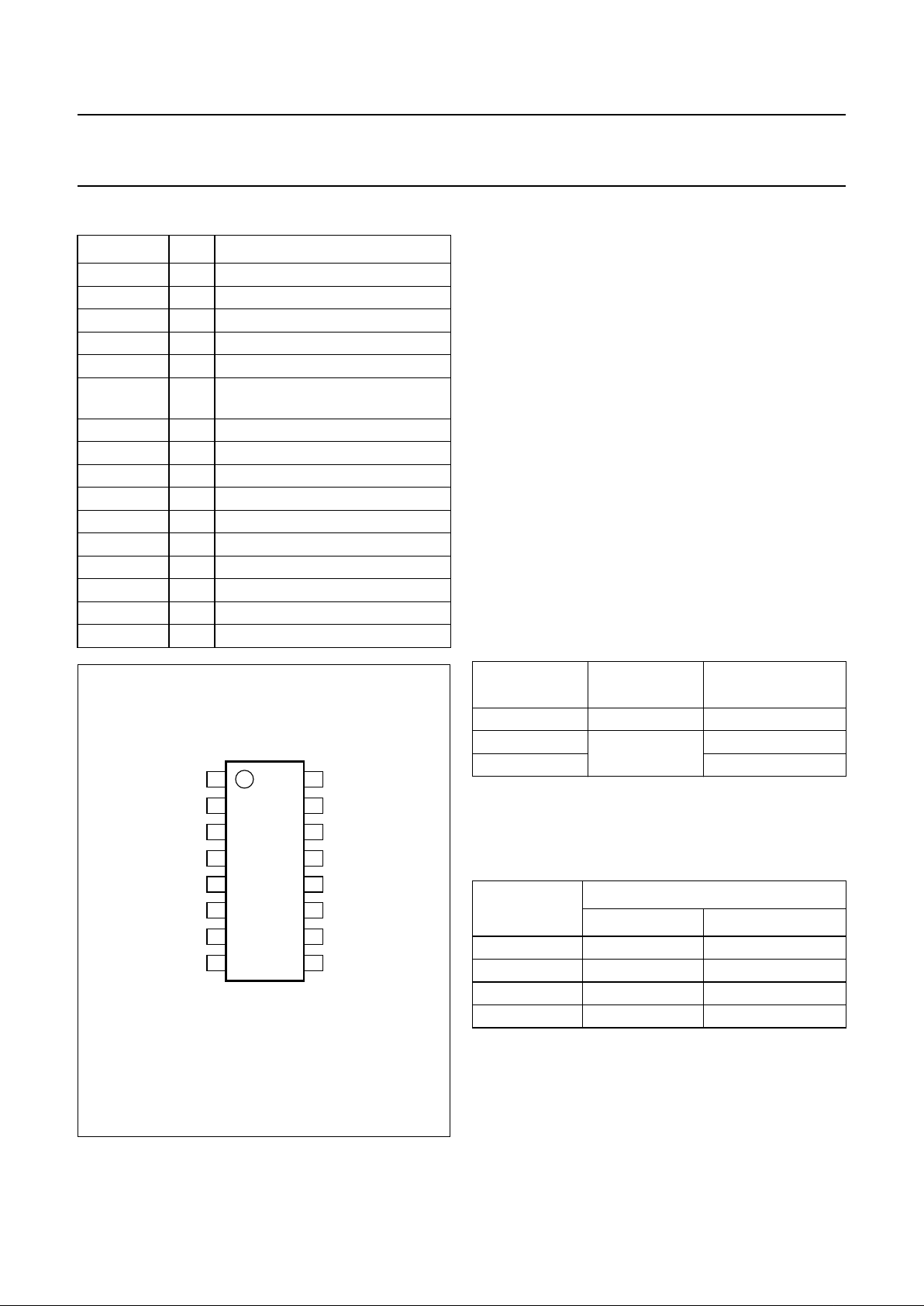
SYMBOL PIN DESCRIPTION
BCK 1 bit clock input
WS 2 word select input
DATAI 3 data input
V
DDD
4 digital supply voltage
V
SSD
5 digital ground
SYSCLK 6 system clock input: 256f
s
, 384f
s
and 512f
s
APPSEL 7 application mode select input
APPL3 8 application input pin 3
APPL2 9 application input pin 2
APPL1 10 application input pin 1
APPL0 11 application input pin 0
V
ref(DAC)
12 DAC reference voltage
V
DDA
13 analog supply voltage for DAC
VOUTL 14 left channel output
V
SSA
15 analog ground for DAC
VOUTR 16 right channel output
Fig.2 Pin configuration.
handbook, halfpage
UDA1324TS
MBK769
1
2
3
4
5
6
7
8
16
15
14
13
12
11
10
9
VOUTR
BCK
V
SSA
WS
VOUTL
DATAI
V
DDA
V
DDD
V
ref(DAC)
V
SSD
APPL0SYSCLK
APPL1APPSEL
APPL2APPL3
VOLTAGE ON
PIN APPSEL
MODE f
sys
V
SSD
L3 mode 256fs, 384fsor 512f
s
0.5V
DDD
static pin mode
384f
s
V
DDD
256f
s
PIN
FUNCTION
L3 MODE STATIC PIN MODE
APPL0 TEST MUTE
APPL1 L3CLOCK DEEM
APPL2 L3MODE SF0
APPL3 L3DATA SF1
2000 Jan 20 5
Philips Semiconductors Preliminary specification
Ultra low-voltage stereo filter DAC UDA1324TS
In the L3 mode, pin APPL0 must be set to LOW. It should
be noted that when the L3 mode is used, an initialization
must be performed when the IC is powered-up.
Digital interface
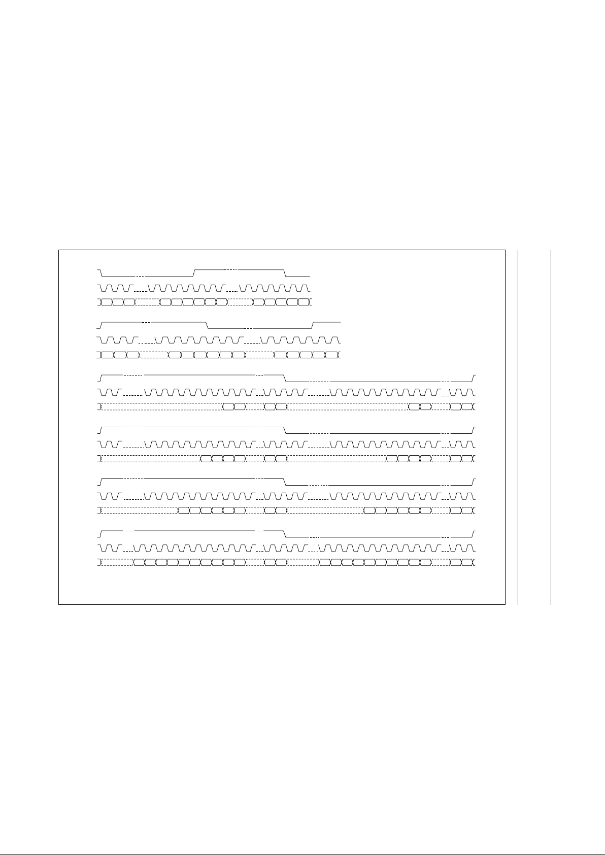
DATA FORMATS
The digital interface of the UDA1324TS supports multiple
format inputs (see Fig.3).
Left and right data-channel words are time multiplexed.
The WS signal must have a 50% duty factor for all
LSB-justified formats.
The BCK clock can be up to 64fs, or in other words the
BCK frequency is 64 times the Word Select (WS)
frequency or less: f
BCK
≤ 64 × fWS.
Important: the WS edge MUST fall on the negative edge
of the BCK at all times for proper operation of the digital
interface.
The UDA1324TS also accepts double speed data for
double speed data monitoring purposes.
L3 MODE
• I2S-bus format with data word length of up to 20 bits
• MSB-justified format with data word length up to 20 bits
• LSB-justified format with data word length of
16, 18 or 20 bits.
STATIC PIN MODE
• I2S-bus format with data word length of up to 20 bits
• LSB-justified format with data word length of
16, 18 or 20 bits.
These four formats are selectable via the static pin codes
SF0 and SF1 (see Table 3).
Table 3 Input format selection using SF0 and SF1
Interpolation filter
Thedigital filter interpolates from1fsto 128fsbycascading
a recursive filter and a FIR filter (see Table 4).
Table 4 Interpolation filter characteristics
Noise shaper
The 3rd-order noise shaper operates at 128f
s
. It shifts
in-band quantization noise to frequencies well above the
audio band. This noise shaping technique enables high
signal-to-noise ratios to be achieved. The noise shaper
output is converted into an analog signal using a Filter
Stream Digital-to-Analog Converter (FSDAC).
Filter stream DAC
The FSDAC is a semi-digital reconstruction filter that
converts the 1-bit data stream of the noise shaper to an
analog output voltage. The filter coefficients are
implemented as current sources and are summed at
virtual ground of the output operational amplifier. In this
way very high signal-to-noise performance and low clock
jitter sensitivity is achieved. A post filter is not needed due
to the inherent filter function of the DAC. On-board
amplifiers convert the FSDAC output current to an output
voltage capable of driving a line output.
The output voltage of the FSDAC scales linearly with the
power supply voltage.
FORMAT SF0 SF1
I2S-bus 0 0
LSB-justified 16 bits 0 1
LSB-justified 18 bits 1 0
LSB-justified 20 bits 1 1
ITEM CONDITION VALUE (dB)
Pass-band ripple 0 to 0.45f
s
±0.1
Stop band >0.55f
s
−50
Dynamic range 0 to 0.45f
s
108
2000 Jan 20 6
Philips Semiconductors Preliminary specification
Ultra low-voltage stereo filter DAC UDA1324TS
This text is here in white to force landscape pages to be rotated correctly when browsing through the pdf in the Acrobat reader.This text is here in
_white to force landscape pages to be rotated correctly when browsing through the pdf in the Acrobat reader.This text is here inThis text is here in
white to force landscape pages toberotatedcorrectlywhenbrowsingthroughthe pdf in the Acrobat reader. white to force landscape pages to be ...
n
dbook, full pagewidth
16
MSB B2 B3 B4 B5 B6
LEFT
LSB-JUSTIFIED FORMAT 20 BITS
WS
BCK
DATA
RIGHT
1518 1720 19 2 1
B19
LSB
16
MSB B2 B3 B4 B5 B6
1518 1720 19 2 1
B19 LSB
MSB MSBB2
21> = 812 3
LEFT
I
2
S-BUS FORMAT
WS
BCK
DATA
RIGHT
3
> = 8
MSB B2
MBL121
16
B5 B6 B7 B8 B9 B10
LEFT
LSB-JUSTIFIED FORMAT 24 BITS
WS
BCK
DATA
RIGHT
1518 1720 1922 212324 2 1
B3 B4
MSB
B2
B23
LSB
16
B5 B6 B7 B8 B9 B10
1518 1720 1922 212324 21
B3 B4
MSB
B2
B23 LSB
16
MSB
B2
LEFT
LSB-JUSTIFIED FORMAT 16 BITS
WS
BCK
DATA
RIGHT
15 2 1
B15
LSB
16
MSB B2
15 2 1
B15 LSB
16
MSB B2 B3 B4
LEFT
LSB-JUSTIFIED FORMAT 18 BITS
WS
BCK
DATA
RIGHT
1518 17 2 1
MSB B2 B3 B4
B17
LSB
16 1518 17 2 1
B17 LSB
MSB-JUSTIFIED FORMAT
WS
LEFT
RIGHT
321321
MSB B2 MSBLSB LSB MSB B2B2
> = 8 > = 8
BCK
DATA
Fig.3 Digital interface input data formats.
 Loading...