

Philips UDA1321PS-N101, UDA1321H-N102, UDA1321H-N101, UDA1321H-N1, UDA1321T-N101 Datasheet
...
DATA SH EET
Preliminary specification
Supersedes data of 1998 May 12
File under Integrated Circuits, IC01
1998 Oct 06
INTEGRATED CIRCUITS
UDA1321
Universal Serial Bus (USB)
Digital-to-Analog Converter (DAC)

1998 Oct 06 2
Philips Semiconductors Preliminary specification
Universal Serial Bus (USB)
Digital-to-Analog Converter (DAC)
UDA1321
FEATURES
General
• Universal Serial Bus (USB) stereo Digital-to-Analog
Converter (DAC) system with adaptive (5 to 55 kHz)
20-bits digital-to-analog conversion and filtering
• USB-compliant audio and Human Interface Device
(HID)
• Supports 12 Mbits/s full-speed serial data transmission
• Supports multiple audio data formats (8, 16 and 24 bits)
• Supports headphone and line output
• Fully automatic ‘Plug-and-Play’ operation
• High linearity
• Wide dynamic range
• Superior signal-to-noise ratio (typical 95 dB)
• Low total harmonic distortion (typical 90 dB)
• 3.3 V power supply
• Efficient power management
• Low power consumption
• On-chip master clock oscillator, only an external crystal
is required
• Partly programmable USB descriptors and configuration
via I
2
C-bus.
Sound processing
• Separate digital volume control for left and right channel
• Soft mute
• Digital bass and treble tone control
• External Digital Sound Processor (DSP) option possible
via standard I
2
S-bus or Japanese digital I/O format
• Selectable clipping prevention
• Selectable Dynamic Bass Boost (DBB)
• On-chip digital de-emphasis.
Document references
•
“USB Specification”
•
“USB Common Class Specification”
•
“USB Device Class Definition for Audio Devices”
•
“Device Class Definition for Human Interface Devices
(HID)”
•
“USB HID Usage Table”
.
APPLICATIONS
• USB monitors
• USB speakers
• USB headsets
• USB telephone/answering machines
• USB links in consumer audio devices.
GENERAL DESCRIPTION
The UDA1321 is a stereo CMOS digital-to-analog
bitstream converter designed for USB-compliant audio
playback devices and multimedia audio
applications.The UDA1321 is an adaptive asynchronous
sink USB audio device with a continuous sampling
frequency (f
s
) range from 5 to 55 kHz. It contains a USB
interface, an embedded microcontroller and an
Asynchronous Digital-to-Analog Converter (ADAC).
The USB interface is the interface between the USB, the
ADAC and the microcontroller. The USB interface consists
of an analog front-end and a USB processor. The analog
front-end transforms the differential USB data to a digital
data stream. The USB processor buffers the input and
output data from the analog front-end and handles all
low-level USB protocols. The USB processor selects the
relevant data from the universal serial bus, performs an
extensive error detection and separates control
information (input and output) and audio information (input
only).
1998 Oct 06 3
Philips Semiconductors Preliminary specification
Universal Serial Bus (USB)
Digital-to-Analog Converter (DAC)
UDA1321
The control information becomes accessible at the
microcontroller. The audio information becomes available
at the digital I/O output or is fed directly to the ADAC.
The microcontroller handles the high-level USB protocols,
translates the incoming control requests and manages the
user interface via General Purpose (GP) pins and an
I2C-bus.
The ADAC enables the wide and continuous range of input
sampling frequencies. By means of a Sample Frequency
Generator (SFG), the ADAC is able to reconstruct the
average sample frequency from the incoming audio
samples. The ADAC also performs the sound processing.
The ADAC consists of FIFO registers, a unique audio
feature processing DSP, the SFG, digital up-sampling
filters, a variable hold register, a Noise Shaper (NS) and a
Filter Stream DAC (FSDAC) with integrated filter and line
output drivers. The audio information is applied to the
ADAC via the USB processor or via the digital I/O input.
An external DSP can be used for adding extra sound
processing features via the digital I/O-bus.
The UDA1321 supports the standard I2S-bus data input
format and the LSB-justified serial data input format with
word lengths of 16, 18 and 20 bits.
The wide dynamic range of the bitstream conversion
technique used in the UDA1321 guarantees a high audio
sound quality.
QUICK REFERENCE DATA
Notes
1. VDD is the supply voltage on pins V
DDA
, V
DDE
, V
DDI
and V
DDX
. VSS is the ground on pins V
SSA
, V
SSE
, V
SSI
and V
SSX
.
All VDD and VSS pins must be connected to the same supply or ground respectively.
2. The audio information from the USB interface is fed directly to the ADAC.
3. The power-save mode (power management) is not supported in the UDA1321/N101;
see Chapter “USB-DAC UDA1321/N101 (Firmware sw 2.1.1.7)”.
SYMBOL PARAMETER CONDITIONS MIN. TYP. MAX. UNIT
Supplies
V
DD
supply voltage note 1 3.0 3.3 3.6 V
I
DD(tot)
total supply current − 50 − mA
I
DD(ps)
supply current in power-save
mode
note 3 − 18 − mA
Dynamic performance DAC
total harmonic
distortion-plus-noise to signal
ratio
fs= 44.1 kHz; RL=5kΩ
at input signal of 1 kHz (0 dB) −−90
(2)
−80 dB
− 0.0032 0.01 %
at input signal of 1 kHz (−60 dB) −−30
(2)
−20 dB
− 3.2 10 %
S/N
bz
signal-to-noise ratio at bipolar
zero
A-weighted at code 0000H 90 95 − dBA
V
o(FS)(rms)
full-scale output voltage
(RMS value)
VDD= 3.3 V − 0.66 − V
General characteristics
f
i(sample)
audio sample input frequency 5 − 55 kHz
T
amb
operating ambient temperature 0 25 70 °C
THD N+
S
---------------------- -

1998 Oct 06 4
Philips Semiconductors Preliminary specification
Universal Serial Bus (USB)
Digital-to-Analog Converter (DAC)
UDA1321
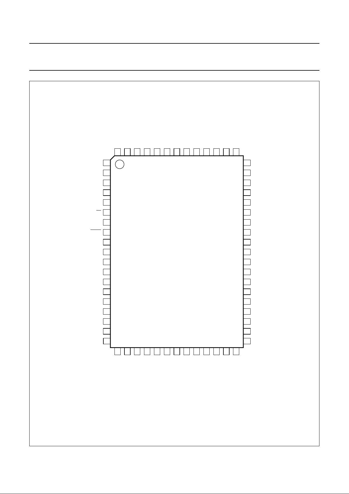
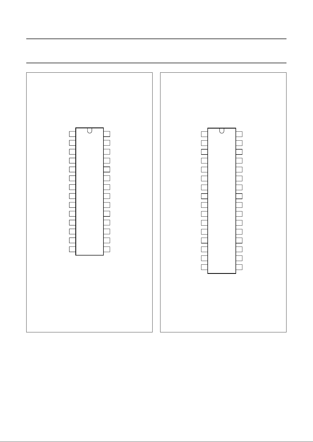
ORDERING INFORMATION
TYPE NUMBER
PACKAGE
NAME DESCRIPTION VERSION
UDA1321H/N101 QFP64 plastic quad flat package; 64 leads (lead length 1.95 mm);
body 14 × 20 × 2.8 mm
SOT319-2
UDA1321T/N101 SO28 plastic small outline package; 28 leads; body width 7.5 mm SOT136-1
UDA1321PS/N101 SDIP32 plastic shrink dual in-line package; 32 leads (400 mil) SOT232-1

1998 Oct 06 5
Philips Semiconductors Preliminary specification
Universal Serial Bus (USB)
Digital-to-Analog Converter (DAC)
UDA1321
BLOCK DIAGRAM
Fig.1 Block diagram.
handbook, full pagewidth
MGM839
ANALOG FRONT-END
D+
USB-PROCESSOR
FIFO REGISTERS
OSC
TEST
CONTROL
BLOCK
MICRO-
CONTROLLER
LEFT
DAC
RIGHT
DAC
TIMING
f
s
f
s
64f
s
128f
s
SAMPLE
FREQUENCY
GENERATOR
UP-SAMPLE FILTERS
VARIABLE HOLD REGISTER
UDA1321H
UDA1321T
UDA1321PS
3rd-ORDER
NOISE SHAPER
REFERENCE
VOLTAGE
AUDIO FEATURE
PROCESSING DSP
DIGITAL I/O
GP4/BCKO
GP2/DO
GP0/BCKI
GP3/WSO
GP1/DI
V
SSX
TC
RTCB
SHTCB
XTAL2
XTAL1
V
DDX
VOUTL
GP5/WSI
SCL
SDA
EA
PSEN
ALE
P2.0
P2.1
P2.2
P2.3
P2.4
P2.5
P2.6
P2.7
P0.0
P0.1
P0.2
P0.3
P0.4
P0.5
P0.6
P0.7
V
DDE
V
SSE
V
SSI
V
DDI
V
DDO
V
SSO
V
DDA
V
SSA
VOUTR
V
ref
D−
1998 Oct 06 6
Philips Semiconductors Preliminary specification
Universal Serial Bus (USB)
Digital-to-Analog Converter (DAC)
UDA1321
PINNING
SYMBOL
PIN
QFP64
PIN
SDIP32
PIN
SO28
I/O DESCRIPTION
GP5/WSI 2 29 25 I/O general purpose pin 5 or word select input
SCL 3 30 26 I/O serial clock input (I
2
C-bus)
SDA 4 31 27 I/O serial data input/output (I
2
C-bus)
P0.7 5 n.a. n.a. I/O Port 0.7 of the microcontroller
EA 6 n.a. n.a. I/O external access (active LOW)
GP1/DI 7 32 28 I/O general purpose pin 1 or data input
PSEN 8 n.a. n.a. I/O program store enable (active LOW)
ALE 9 n.a. n.a. I/O address latch enable (active HIGH)
GP2/DO 10 1 1 I/O general purpose pin 2 or data output for extra DSP
chip
P2.0 11 n.a. n.a. I/O Port 2.0 of the microcontroller
P2.1 12 n.a. n.a. I/O Port 2.1 of the microcontroller
GP3/WSO 13 2 2 I/O general purpose pin 3 or master word select output for
extra DSP chip
GP4/BCKO 14 3 3 I/O general purpose pin 4 or master bit clock output for
extra DSP chip
SHTCB 15 4 4 I shift clock TCB input (active HIGH)
D− 17 6 5 I/O negative data line of the differential data bus conform
to the USB-standard
P2.2 18 n.a. n.a. I/O Port 2.2 of the microcontroller
P2.3 19 n.a. n.a. I/O Port 2.3 of the microcontroller
D+ 20 7 6 I/O positive data line of the differential data bus conform to
the USB-standard
P2.4 21 n.a. n.a. I/O Port 2.4 of the microcontroller
P2.5 22 n.a. n.a. I/O Port 2.5 of the microcontroller
P2.6 23 n.a. n.a. I/O Port 2.6 of the microcontroller
P2.7 24 n.a. n.a. I/O Port 2.7 of the microcontroller
V
DDI
25 8 7 − digital supply voltage core
V
SSI
29 9 8 − digital ground core
V
SSE
30 10 9 − digital ground I/O pins
V
DDE
32 11 10 − digital supply voltage I/O pins
V
SSX
36 13 11 − crystal oscillator ground
XTAL1 37 14 12 I crystal oscillator input1
XTAL2 38 15 13 O crystal oscillator output 2
V
DDX
39 16 14 − crystal oscillator supply voltage
V
ref
42 18 15 O reference output voltage
V
SSA
44 19 16 − analog ground
V
DDA
45 20 17 − analog supply voltage
VOUTR 46 21 18 O right channel output voltage
V
SSO
49 22 19 − operational amplifier ground
1998 Oct 06 7
Philips Semiconductors Preliminary specification
Universal Serial Bus (USB)
Digital-to-Analog Converter (DAC)
UDA1321
V
DDO
51 23 20 − operational amplifier supply voltage
VOUTL 53 24 21 O left channel output voltage
TC 55 25 22 I test control input (active HIGH)
P0.0 56 n.a. n.a. I/O Port 0.0 of the microcontroller
P0.1 57 n.a. n.a. I/O Port 0.1 of the microcontroller
P0.2 58 n.a. n.a. I/O Port 0.2 of the microcontroller
P0.3 59 n.a. n.a. I/O Port 0.3 of the microcontroller
P0.4 60 n.a. n.a. I/O Port 0.4 of the microcontroller
RTCB 61 26 23 I asynchronous reset input for test control box (active
HIGH)
P0.5 62 n.a. n.a. I/O Port 0.5 of the microcontroller
P0.6 63 n.a. n.a. I/O Port 0.6 of the microcontroller
GP0/BCKI 64 27 24 I/O general purpose pin 0 or master bit clock input
n.c. 1, 16, 26,
27, 28, 31,
33, 34, 35,
40, 41, 43,
47, 48, 50,
52, 54
5, 12, 17,
28
n.a. − not connected
SYMBOL
PIN
QFP64
PIN
SDIP32
PIN
SO28
I/O DESCRIPTION
1998 Oct 06 8
Philips Semiconductors Preliminary specification
Universal Serial Bus (USB)
Digital-to-Analog Converter (DAC)
UDA1321
Fig.2 Pin configuration QFP64.
handbook, full pagewidth
UDA1321H
MGM850
1
2
3
4
5
6
7
8
9
10
11
12
13
14
15
16
17
18
19
n.c.
GP5/WSI
SCL
SDA
P0.7
EA
GP1/DI
PSEN
ALE
GP2/DO
P2.0
P2.1
GP3/WSO
GP4/BCKO
SHTCB
n.c.
D−
P2.2
P2.3
V
DDO
n.c.
V
SSO
n.c.
n.c.
VOUTR
V
DDA
V
SSA
n.c.
V
REF
n.c.
n.c.
V
DDX
XTAL2
XTAL1
V
SSX
n.c.
n.c.
n.c.
51
50
49
48
47
46
45
44
43
42
41
40
39
38
37
36
35
34
33
20
21
22
23
24
25
26
27
28
29
30
31
32
64
63
62
61
60
59
58
57
56
55
54
53
52
GP0/BCKI
P0.6
P0.5
RTCB
P0.4
P0.3
P0.2
P0.1
P0.0
TC
n.c.
VOUTL
n.c.
D+
P2.4
P2.5
P2.6
P2.7
V
DDI
n.c.
n.c.
n.c.
V
SSI
V
SSE
n.c.
V
DDE
1998 Oct 06 9
Philips Semiconductors Preliminary specification
Universal Serial Bus (USB)
Digital-to-Analog Converter (DAC)
UDA1321
Fig.3 Pin configuration SO28.
handbook, halfpage
GP2/DO
GP3/WSO
GP4/BCKO
SHTCB
D−
D+
V
DDI
V
SSI
V
SSE
V
DDE
V
SSX
XTAL1
XTAL2
V
DDX
GP1/DI
SDA
SCL
GP5/WSI
RTCB
TC
GP0/BCKI
VOUTL
V
DDO
V
SSO
VOUTR
V
DDA
V
SSA
V
ref
1
2
3
4
5
6
7
8
9
10
11
12
13
28
27
26
25
24
23
22
21
20
19
18
17
16
1514
UDA1321T
MGM840
Fig.4 Pin configuration SDIP32.
handbook, halfpage
UDA1321PS
MGM841
1
2
3
4
5
6
7
8
9
10
11
12
13
14
15
16
32
31
30
29
28
27
26
25
24
23
22
21
20
19
18
17
GP2/DO GP1/DI
GP3/WSO SDA
GP4/BCKO SCL
SHTCB GP5/WSI
n.c.
n.c.
n.c.
D− GP0/BCKI
D+ RTCB
V
DDI
V
SSI
V
SSE
V
DDE
V
SSX
V
DDX
TC
VOUTL
VOUTR
XTAL1
V
SSA
V
DDA
V
SSO
V
DDO
XTAL2
V
ref
n.c.

1998 Oct 06 10
Philips Semiconductors Preliminary specification
Universal Serial Bus (USB)
Digital-to-Analog Converter (DAC)
UDA1321
FUNCTIONAL DESCRIPTION
All bold-faced parameters given in this data sheet
such as ‘bAlternateSetting’ are part of the USB
specification as described in
“USB Device Class
Definition for Audio Devices”
.
The Universal Serial Bus (USB)
Data and power are transferred via the USB by a 4-wire
cable. The signalling occurs via two wires and
point-to-point segments. The signals on each segment are
differentially driven into a cable of 90 Ω intrinsic
impedance. The differential receiver features input
sensitivity of at least 200 mV and sufficient common mode
rejection.
The analog front-end
The analog front-end is an on-chip generic USB
transceiver. It is designed to allow voltage levels up to V
DD
from standard or programmable logic to interface with the
physical layer of the USB. It is capable of receiving and
transmitting serial data at full speed (12 Mbits/s).
The USB processor
The USB processor forms the interface between the
analog front-end, the ADAC and the microcontroller.
The USB processor consists of:
• The Philips Serial Interface Engine (PSIE)
• The Memory Management Unit (MMU)
• The Audio Sample Redistribution (ASR) module.
T
HE PHILIPS SERIAL INTERFACE ENGINE AND MEMORY
MANAGEMENT UNIT (PSIE AND MMU)
The PSIE and MMU translate the electrical USB signals
into bytes and signals. Depending upon the USB device
address and the USB endpoint address, the USB data is
directed to the correct endpoint buffer on the PSIE and
MMU interface. The data transfer could be of the bulk,
isochronous, control or interrupt type. The USB device
address is configured during the enumeration process.
The UDA1321 has three endpoints. These are:
• Control endpoint 0
• Status interrupt endpoint
• Isochronous data sink endpoint.
The amount of bytes per packet on the control endpoint is
limited by the PSIE and MMU hardware to 8 bytes per
packet.
The PSIE is the digital front-end of the USB processor.This
module recovers the 12 MHz USB clock, detects the USB
sync word and handles all low-level USB protocols and
error checking.
The MMU is the digital back-end of the USB processor.
It handles the temporary data storage of all USB packets
that are received or sent over the bus. Three types of
packets are defined on the USB. These are:
• Token packets
• Data packets
• Handshake packets.
The token packet contains information about the
destination of the data packet. The audio data is
transferred via an isochronous data sink endpoint and
consequently no handshaking mechanism is used.
The MMU also generates a 1 kHz clock that is locked to
the USB Start-Of-Frame (SOF) token.
T
HE AUDIO SAMPLE REDISTRIBUTION (ASR) MODULE
The ASR module reads the audio samples from the MMU
and distributes these samples equidistant over a 1 ms
frame period. The distributed audio samples are translated
by the digital I/O module to standard I2S-bus format or
Japanese digital I/O format. The ASR module generates
the bit clock and the word select signal of the digital I/O.
The digital I/O formats the received audio samples to one
of the four specified serial digital audio formats
(standard I2S-bus, 16, 18 or 20 bits LSB-justified).
The microcontroller
The microcontroller receives the control information
selected from the USB by the USB processor. It handles
the high-level USB protocols and the user interfaces.
The major task of the software process, that is mapped
upon the microcontroller, is to control the different modules
of the UDA1321 in such a way that it behaves as a USB
device. Therefore the microcontroller:
• Interprets the USB requests and maps them upon the
UDA1321 application
• Controls the internal operation of the UDA1321 and the
digital I/O pins
• Communicates with the external world (EEPROM) using
the I
2
C-bus facility and the general purpose I/O pins.

1998 Oct 06 11
Philips Semiconductors Preliminary specification
Universal Serial Bus (USB)
Digital-to-Analog Converter (DAC)
UDA1321
The Asynchronous Digital-to-Analog Converter
(ADAC)
The ADAC receives USB audio information from the USB
processor or from the digital I/O-bus. The ADAC is able to
reconstruct the sample clock from the rate at which the
audio samples arrive and handles the audio sound
processing. After processing, the audio signal is
up-sampled, noise-shaped and converted to analog output
voltages capable of driving a line output. The ADAC
consists of:
• A Sample Frequency Generator (SFG)
• First-In First-Out (FIFO) registers
• An audio feature processing DSP
• Two digital up-sample filters
• A variable hold register
• A digital Noise Shaper (NS)
• A Filter Stream DAC (FSDAC) with integrated filter and
line output drivers.
THE SAMPLE FREQUENCY GENERATOR (SFG)
The SFG controls the timing signals for the asynchronous
digital-to-analog conversion. By means of a digital PLL,
the SFG automatically recovers the applied sampling
frequency and generates the accurate timing signals for
the audio feature processing DSP and the up-sample
filters.
F
IRST-IN FIRST-OUT (FIFO) REGISTERS
The FIFO registers are used to store the audio samples
temporarily coming from the USB processor or from the
digital I/O input. The use of a FIFO register (in conjunction
with the SFG) is necessary to remove all jitter present on
the incoming audio signal.
T
HE AUDIO FEATURE PROCESSING DSP
A DSP processes the sound features. The control and
mapping of the sound features is explained in Section
“Controlling the USB Digital-to-Analog Converter (DAC)”.
Depending on the sampling rate (fs) the DSP has four
frequency domains in which the treble and bass are
regulated (see Table 1). The domain is chosen
automatically.
T
HE UP-SAMPLE FILTERS AND VARIABLE HOLD REGISTER
After the audio feature processing DSP two up-sample
filters and a variable hold register increase the
oversampling rate to 128fs.
Table 1 Frequency domains for audio processing
T
HE NOISE SHAPER
A 3rd-order noise shaper converts the oversampled data
to a noise-shaped bitstream for the FSDAC. The in-band
quantization noise is shifted to frequencies well above the
audio band.
T
HE FILTER STREAM DAC (FSDAC)
The FSDAC is a semi-digital reconstruction filter that
converts the 1-bit data stream of the noise shaper to an
analog output voltage. The filter coefficients are
implemented as current sources and are summed at
virtual ground of the output operational amplifier. In this
way very high signal-to-noise performance and low clock
jitter sensitivity is achieved. A post filter is not needed
because of the inherent filter function of the DAC.
On-board amplifiers convert the FSDAC output current to
an output voltage signal capable of driving a line output.
USB Digital-to-Analog Converter (DAC) descriptors
In a typical USB environment the USB host has to know
which kind of devices are connected. For this purpose
each device contains a number of USB descriptors. These
descriptors describe, from different points of view (USB
configuration, USB interface and USB endpoint), the
capabilities of a device. Each of them can be requested by
the host. The collection of descriptors is denoted as a
descriptor map. This descriptor map will be reported to the
USB host during enumeration and on request.
The full descriptor map is implemented in the firmware
exploiting the full functionality of the UDA1321. The USB
descriptors and their most important fields, in relationship
to the characteristics of the UDA1321 are briefly explained
below.
G
ENERAL DESCRIPTORS
The UDA1321 supports one configuration containing a
control interface, an audio interface and a HID interface.
The descriptor map that describes this configuration is
partly fixed and partly programmable.
DOMAIN SAMPLE FREQUENCY (kHz)
1 5 to 12
212to25
325to40
440to55
1998 Oct 06 12
Philips Semiconductors Preliminary specification
Universal Serial Bus (USB)
Digital-to-Analog Converter (DAC)
UDA1321
Fig.5 Audio function topology.
handbook, full pagewidth
MBK530
INPUT TERMINAL
OUTPUT TERMINAL
FEATURE UNIT
FU
IT
OT
The programmable part can be retrieved from one of four
configuration maps located in the firmware or from an
I2C-bus EEPROM. At start-up one of four configuration
maps can be selected depending on the logical
combination of GP3 and GP0. It is possible to overwrite
this configuration map with a configuration map loaded
from an I2C-bus EEPROM.
A
UDIO DEVICE CLASS SPECIFIC DESCRIPTORS
The audio device class is partly specified with standard
descriptors and partly with specific audio device class
descriptors. The standard descriptors specify the number
and the type of the interface or endpoint. The UDA1321
supports 7 different audio modes:
• 8-bit Pulse Code Modulation (PCM) mono or stereo
audio data
• 16-bit PCM mono or stereo audio data
• 24-bit PCM mono or stereo audio data
• Zero bandwidth mode.
Each mode is defined as an alternate setting of the audio
interface, selectable with the standard audio streaming
interface descriptor bAlternateSetting field.
The seven alternate settings are described in more detail
by the specific audio device class descriptors.
The UDA1321 supports the Input Terminal (IT), Output
Terminal (OT) and the Feature Unit (FU) descriptors.
The input and output terminals are not controllable via the
USB. The feature unit provides the basic manipulation of
the incoming logical channels.
The supported sound features are:
• Volume control
• Mute control
• Treble control
• Bass control
• Bass boost control.
Table 2 Audio bandwidth at each audio mode
The maximum number of audio data samples within a USB
packet arriving on the isochronous sink endpoint is
restricted by the buffer capacity of this isochronous
endpoint. The maximum buffer capacity is 336 bytes/ms.
For each alternate setting with audio, a maximum
bandwidth is claimed as indicated in the standard
isochronous audio data endpoint descriptor
wMaxPacketSize field. To allow a small overshoot in the
number of audio samples per packet, the top sample
frequency of 55 kHz is taken in the calculation of the
bandwidth for each alternate setting. For each alternate
setting, with its own isochronous audio data endpoint
descriptor, wMaxPacketSize field is then defined as
described in Table 2.
Although in a specific UDA1321 application no endpoint
control properties can be used upon the isochronous
adaptive sink endpoint, the descriptors are still necessary
to inform the host about the definition of this endpoint:
isochronous, adaptive, sink, continuous sampling
frequency (at input side of this endpoint) with lower bound
of 5 kHz and upper bound of 55 kHz.
The audio class specific descriptors can be requested with
the ‘Get descriptor: configuration request’, which returns
all the descriptors, except the device descriptor.
H
UMAN INTERFACE DEVICE SPECIFIC DESCRIPTORS
The inputs defined on the UDA1321 are transmitted via the
USB to the host according to the HID class. The host
AUDIO MODE wMaxPacketSize
8-bit PCM; mono 56 (8⁄8× 1 × 56)
8-bit PCM; stereo 112 (8⁄8× 2 × 56)
16-bit PCM; mono 112 (16⁄8× 1 × 56)
16-bit PCM; stereo 224 (16⁄8× 2 × 56)
24-bit PCM; mono 168 (24⁄8× 1 × 56)
24-bit PCM; stereo 336 (24⁄8× 2 × 56)

1998 Oct 06 13
Philips Semiconductors Preliminary specification
Universal Serial Bus (USB)
Digital-to-Analog Converter (DAC)
UDA1321
responds with the appropriate settings via the audio device
class for the audio related parts or via the HID class for the
HID related inputs and outputs of the UDA1321.
A HID descriptor is necessary to inform the host about the
conception of the user interface. The host communicates
via the HID device driver using either the control pipe or
the interrupt pipe. The UDA1321 uses USB endpoint 0
(control pipe) to respond to the HID specific ‘Get/set report
request’ to receive or transmit data from or to the
UDA1321. The UDA1321 uses the status interrupt
endpoint as interrupt pipe for polling asynchronous data.
The UDA1321 is a high-speed device. The maximum
transaction size is 64 bytes per USB frame and the polling
rate is defined at a maximum of every 1 ms.
The host requests the configuration descriptor which
includes the standard interface descriptor, the HID
endpoint descriptor and the HID descriptor. The HID
device driver of the host then requests the report
descriptor.
Report descriptors are composed of pieces of information
about the device. Each piece of information is called an
item. All items have a 1-byte prefix that contains the item
tag, type and size. In the UDA1321 only the short item
basic type is used.
The hosts HID device driver will parse the report descriptor
and the defined items. By examining all of these items, the
HID class driver is able to determine the size and
composition of data reports from the device.
The main items of the UDA1321 are input and output
reports. Input reports are sent via the interrupt pipe
(UDA1321 USB address 3). Input and output reports can
be requested by the host via the control endpoint (USB
address 0).
The UDA1321 supports a maximum of three pushbuttons,
which represents a certain feature of the UDA1321. If
pressed by the user the pushbutton will go to its ‘ON’ state,
if not pressed the pushbutton will go back to its ‘OFF’ state.
The UDA1321 supports a maximum of two outputs for e.g.
user LEDs.
For more information about the input and output functions
of the UDA1321 see the application documentation of the
device.
Controlling the USB Digital-to-Analog Converter
(DAC)
This section describes the functionality of the feature unit
of the UDA1321. The mapping of this functionality onto
USB descriptors is as implemented in the firmware.
The sound features as defined in the
“USB Device Class
Definition for Audio Devices”
are mapped on the UDA1321
specific feature registers by the microcontroller. These
specific sound features are:
• Volume control (separate for left and right stereo
channels, no master channel)
• Mute control (only master channel)
• Treble control (only master channel)
• Bass control (only master channel)
• Dynamic bass boost control (only master channel).
These specific features can be activated via the host
(audio device class requests) or via the GP pins (HID plus
audio device class requests). Via the I2C-bus the user is
able to download the necessary configuration data for
different applications (definition of the function of the GP
pins, with or without digital I/O functionality, etc.).
The mapping and control of the standard USB audio
features and UDA1321 specific features is described
below.
V
OLUME CONTROL
Volume control is possible via the host or via predefined
GP pins. The setting of 0 dB is always referenced to the
maximum available volume setting. Table 3 gives the
mapping of wVolume value (as defined in the
“USB
Device Class Definition for Audio Devices”
) upon the
actual volume setting of the USB DAC. When using the
UDA1321, the range is 0 down to−60 dB (in steps of 1 dB)
and −∞ dB. Independant control of ‘left’/’right’ volume is
possible. It should be noted that wVolume bits B7 to B0
are not used. Values above 0 dB are returned as 0 dB.
The volume value at start-up of the device is defined in the
selected configuration map.
Balance control is possible via the separate volume control
option of both channels. Therefore the characteristics of
the balance control are equal to the volume control
characteristics.
1998 Oct 06 14
Philips Semiconductors Preliminary specification
Universal Serial Bus (USB)
Digital-to-Analog Converter (DAC)
UDA1321
Table 3 Volume control characteristics; note 1
Note
1. The volume control characteristics of this table are in accordance with the latest Audio Device Class Definition.
The volume control characteristics of the UDA1321/N101 are slightly different; see Chapter “USB-DAC
UDA1321/N101 (Firmware sw 2.1.1.7)”
wVOLUME
VOLUME USB SIDE
(dB)
VOLUME USB DAC
(dB)
B15 B14 B13 B12 B11 B10 B9 B8
00000000 0 0
11111111 −1 −1
11111110 −2 −2
11111101 −3 −3
11111100 −4 −4
11111011 −5 −5
11111010 −6 −6
11111001 −7 −7
11111000 −8 −8
11110111 −9 −9
11110110 −10 −10
... ... ... ... ... ... ... ... ... ...
11000101 −59 −59
11000100 −60 −60
11000011 −61 −∞
11000010 −62 −∞
... ... ... ... ... ... ... ... ... ...
10000000 −∞ −∞
MUTE CONTROL
Mute is one of the sound features as defined in the
“USB
Device Class Definition for Audio Devices”
. The mute
control request data bMute controls the position of the
mute switch. The position can be either on or off. When
bMute is true the feature unit is muted. When bMute is
false the feature unit is not muted.
When the mute is active for the master channel, the value
of the sample is decreased smoothly to zero following a
raised cosine curve. There are 32 coefficients used to step
down the value of the data, each one being used 32 times
before stepping to the next.
This amounts to a mute transition of 23 ms at
f
s
= 44.1 kHz. When the mute is released, the samples are
returned to the full level again following a raised cosine
curve with the same coefficients being used in reversed
order. The mute, on the master channel is synchronized to
the sample clock, so that operation always takes place on
complete samples.
A mute can be given via the host or by pressing a
predefined GP pin.
 Loading...