

Philips UAA3535HL Datasheet

INTEGRATED CIRCUITS
DATA SH EET
UAA3535HL
Low power GSM/DCS/PCS
multi-band transceiver
Objective specification
File under Integrated Circuits, IC17
2000 Feb 17

Philips Semiconductors Objective specification
Low power GSM/DCS/PCS multi-band transceiver UAA3535HL
FEATURES
• Multi-band application for GSM, DCS and PCS cellular
phone systems
• Low noise and wide dynamic range low IF receiver
• More than 35 dB on-chip image rejection in receive
mode
• More than 64 dB gain control range in receive mode
• Integrated channel filter
• Integrated TX low-pass filter
• High precision I/Q modulator
• Multi-band TX modulation loop architecture including
offset mixer and phase-frequency detector
• Dual PLL with on-chip fully integrated IF VCO
• Fully differential design minimizing crosstalk and
spurious signals
• Functional down to 2.4 V and up to 3.6 V
• 3-wire serial bus interface
• LQFP48 package.
APPLICATIONS
• GSM 900 MHz, DCS 1800 MHz and PCS 1900 MHz
hand-held transceivers.
GENERAL DESCRIPTION
The UAA3535HL is intended for Global Systems for
Mobile communication (GSM), Digital Cellular
communication Systems (DCS) and Personal
Communication Services (PCS).The circuit integrates the
receiver and most of the transmitter section of hand-held
transceivers for these applications.
The receiver consists of two sections. The first section is
the RF receiver front-end, which amplifies the GSM, DCS
or PCS aerial signal, then converts the chosen channel
down to a low Intermediate Frequency (IF) of 100 kHz,
and also provides more than 35 dB image suppression.
Some selectivity is provided at this stage by an on-chip
low-passfilter andchannel selectivity isprovided bya high
performance integrated band-pass filter.
The second section is the IF section, which further
amplifies the chosen channel and performs gain control to
adjust the output level to the desired value. The IF gain
can be varied over more than 64 dB gain range.
The transmitteralso consists oftwo sections. The first is a
highprecision I/Q modulatorwhichconverts thebaseband
modulation up to the transmit IF. The second is a
modulation loop architecture which converts the signal
to RF.
The Local Oscillator (LO) signals are provided by an
on-chip Voltage Controlled Oscillator (VCO) for operation
of the IF section and are provided externally for operation
ofthe RF section.The frequenciesof theRF and IF VCOs
are set by internal PLL circuits, which are programmable
via a 3-wire serial bus. Comparison frequencies are
200 kHz (100 kHz step programmability) and 13 MHz for
the RF and IF PLL respectively, and are derived from a
13 MHz reference signal which has to be supplied
externally. The quadrature-phase RF LO signals required
for I/Q mixers in reception are generated internally.
The quadrature LO signals required for operation of the
I/Q modulator are generated inside the IF VCO.
The circuit can be powered-up into one of three different
modes: RX, TX or SYN mode, depending on the logic
state of pins RXON, TXON and SYNON, respectively. It is
also possible to set the IC in one of these modes by
software, using the 3-wire bus serial programming.
In RX (TX) mode, all sections required for receive
(transmit) are turned on. The SYN mode is used to
power-up the synthesizers prior to the RX or TX mode.
In the SYN mode, some internal LO buffers are also
powered-up in such a way that VCO pulling is minimized
when switching on the receiver or the transmitter.
Additional band selection is done using the 3-wire bus
serial programming, allowing the required enabling of the
Low Noise Amplifiers (LNAs) and charge pumps current
programming.
ORDERING INFORMATION
TYPE
NUMBER
UAA3535HL LQFP48 plastic low profile quad flat package; 48 leads; body 7 × 7 × 1.4 mm SOT313-2
2000 Feb 17 2
NAME DESCRIPTION VERSION
PACKAGE
Philips Semiconductors Objective specification
Low power GSM/DCS/PCS multi-band transceiver UAA3535HL
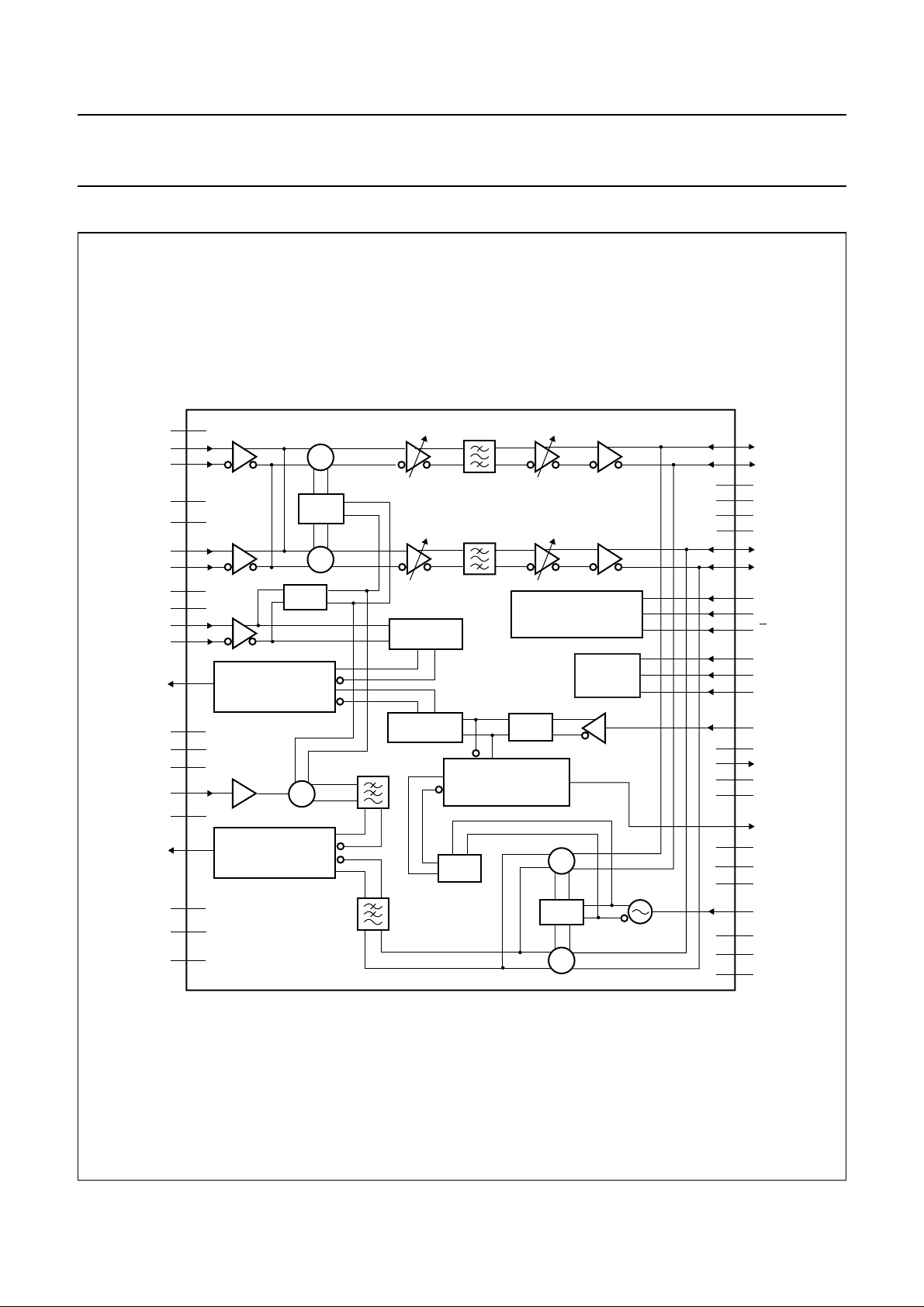
BLOCK DIAGRAM
handbook, full pagewidth
RFGND1
GSMIA
GSMIB
RFGND2
V
CC(RF)
DCSPCSIA
DCSPCSIB
RFLOGND
V
CC(RFLO)
RFLOIA
RFLOIB
RFCPO
RFCPGND
V
CC(RFCP)
RFGND3
TXRFI
V
CC(TXCP)
TXCPO
TXCPGND
RFGND4
EXTRES
38
39
40
41
37
42
43
29
32
30
31
PHASE-FREQUENCY
24
DETECTOR AND
CHARGE PUMP
23
26
44
45
2
PHASE-FREQUENCY
1
DETECTOR AND
CHARGE PUMP
48
46
47
UAA3535HL
QUAD
1 : 1/2
×
7
IA
36
35
34
33
10
16
17
18
11
12
25
22
14
15
20
21
19
13
28
27
FCA074
8
9
3
5
4
6
IB
IFCIA
IFCIB
IFCQA
IFCQB
QA
QB
DATA
CLK
E
RXON
TXON
SYNON
REFIN
TXIFA
TSTO
V
CC2(IF)
IFGND2
IFCPO
IFCPGND
V
CC(IFCP)
IFGND1
IFTUNE
V
CC1(IF)
SYNGND
V
CC(SYN)
×
×
3-WIRE BUS
MAIN
DIVIDER
REFERENCE
DIVIDER
1 : 6/7
PHASE-FREQUENCY
DETECTOR AND
CHARGE PUMP
CONTROL REGISTER
POWER
ENABLE
1 : 1/2
×
1 : 1/2
91 MHz GSM/DCS
78 MHz PCS
×
Fig.1 Block diagram.
2000 Feb 17 3
Philips Semiconductors Objective specification
Low power GSM/DCS/PCS multi-band transceiver UAA3535HL
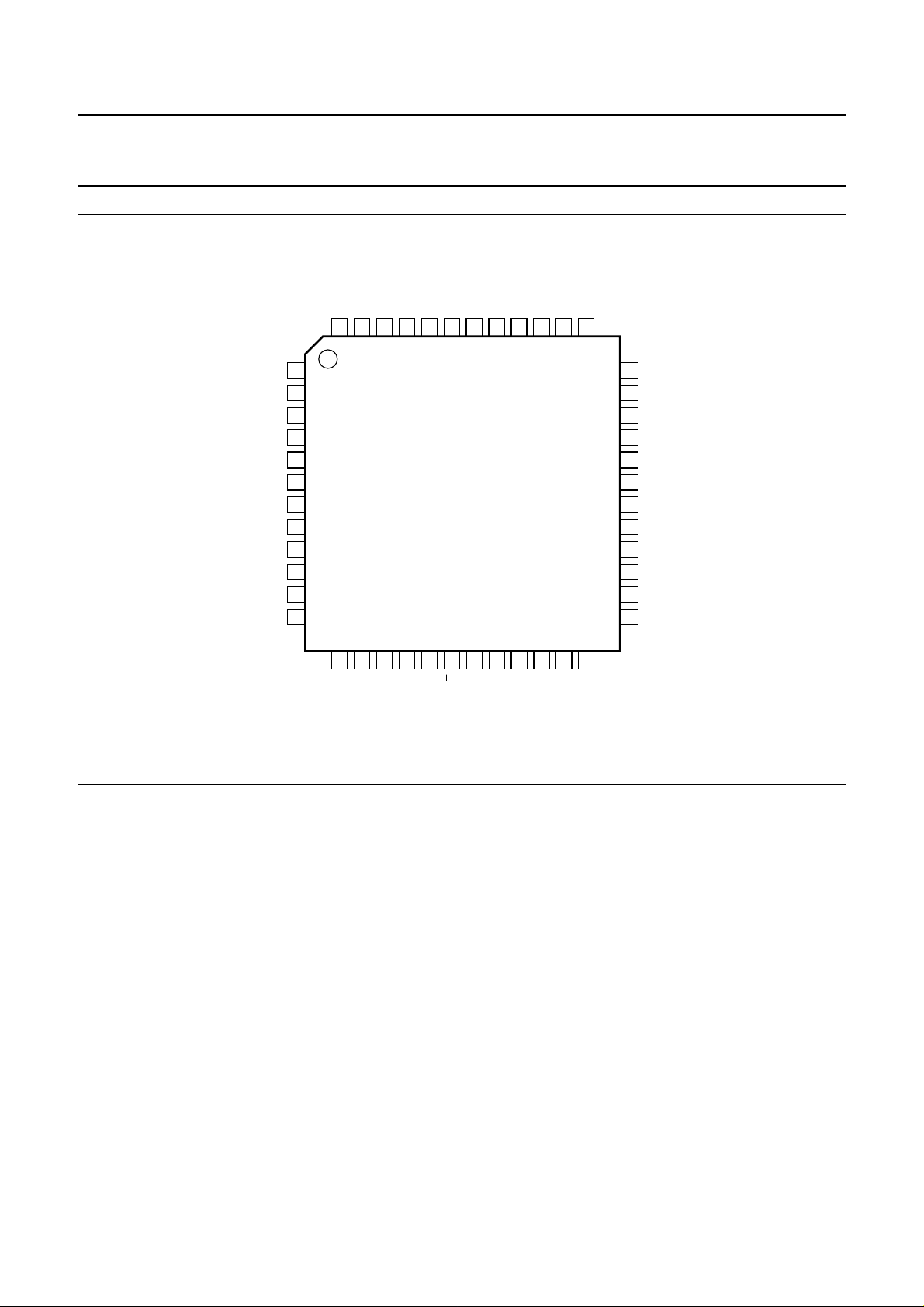
PINNING
SYMBOL PIN DESCRIPTION
TXCPO 1 transmit modulation loop GSM
charge pump output
V
CC(TXCP)
2 transmit modulation loop charge
pump supply voltage
TXIFA 3 transmit IF test pin
IFGND1 4 IF ground 1
TSTO 5 test mode output
V
CC1(IF)
6 IF supply voltage 1
IA 7 I path A baseband input/output
IB 8 I path B baseband input/output
QA 9 Q path A baseband input/output
QB 10 Q path B baseband input/output
RXON 11 RX mode control input
TXON 12 TX mode control input
IFTUNE 13 transmit IF VCO tune input
V
CC2(IF)
14 IF supply voltage 2
IFGND2 15 IF ground 2
DATA 16 3-wire bus data input
CLK 17 3-wire bus clock input
E 18 3-wire bus enable control input
(active LOW)
V
CC(IFCP)
19 transmit IF charge pump supply
voltage
IFCPO 20 transmit IF charge pump output
IFCPGND 21 transmit IF charge pump ground
REFIN 22 synthesizers reference input
RFCPGND 23 RF charge pump ground
RFCPO 24 RF charge pump output
SYNON 25 SYN mode control input
SYMBOL PIN DESCRIPTION
V
CC(RFCP)
V
CC(SYN)
26 RF charge pump supply voltage
27 synthesizers supply voltage
SYNGND 28 synthesizers ground
RFLOGND 29 RF LO ground
RFLOIA 30 RF LO input A
RFLOIB 31 RF LO input B
V
CC(RFLO)
32 RF LO supply voltage
IFCQB 33 RX IF Q test pin B
IFCQA 34 RX IF Q test pin A
IFCIB 35 RX IF I test pin B
IFCIA 36 RX IF I test pin A
V
CC(RF)
37 RF front-end and transmit
modulation loop supply voltage
RFGND1 38 RF front-end and transmit
modulation loop ground 1
GSMIA 39 receiver GSM RF input A
GSMIB 40 receiver GSM RF input B
RFGND2 41 RF front-end and transmit
modulation loop ground 2
DCSPCSIA 42 receiver DCS/PCS RF input A
DCSPCSIB 43 receiver DCS/PCS RF input B
RFGND3 44 RF front-end and transmit
modulation loop ground 3
TXRFI 45 input from RF transmit VCOs
RFGND4 46 RF front-end and transmit
modulation loop ground 4
EXTRES 47 reference resistor for transmit
modulation loop
TXCPGND 48 transmit modulation loop charge
pump ground
2000 Feb 17 4
Philips Semiconductors Objective specification
Low power GSM/DCS/PCS multi-band transceiver UAA3535HL
handbook, full pagewidth
TXCPO
V
CC(TXCP)
TXIFA
IFGND1
TSTO
V
CC1(IF)
RXON
TXON
QA
QB
RFGND4
EXTRES
47
46
14
15
IFGND2
CC2(IF)
V
TXRFI
RFGND3
45
44
UAA3535HL
16
17
CLK
DATA
TXCPGND
48
1
2
3
4
5
6
IA
7
IB
8
9
10
11
12
13
IFTUNE
DCSPCSIA
DCSPCSIB
43
42
18
19
E
CC(IFCP)
V
RFGND2
GSMIB
41
40
21
20
IFCPO
IFCPGND
RFGND1
GSMIA
39
38
22
23
REFIN
RFCPGND
CC(RF)
V
24 37
RFCPO
36
IFCIA
35
IFCIB
34
IFCQA
33
IFCQB
V
32
31
RFLOIB
RFLOIA
30
29
RFLOGND
SYNGND
28
V
27
V
26
SYNON
25
FCA068
CC(RFLO)
CC(SYN)
CC(RFCP)
Fig.2 Pin configuration.
FUNCTIONAL DESCRIPTION
RF receiver
The receiver front-end converts the aerial RF signal from
EGSM (Extended GSM; 925 to 960 MHz), DCS
(1805 to 1880 MHz) or PCS (1930 to 1990 MHz) bands
down to an IF signal of 100 kHz. The first stages are
symmetricalLNAs thatarematched to50 Ωusing external
baluns. The LNAs are followed by an I/Q down-mixer.
The I/Q down-mixer consists of two mixers in parallel but
driven by quadrature out of phase LO signals.
The In-phase (I)and Quadrature- phase (Q)IF signalsare
then low-pass filtered to provide protection from high
frequency offset interferers. The IF I and Q signals are
then fed into the channel filter.
2000 Feb 17 5
Channel filter and AGC
The front-end IF I and Q outputs are first applied to an
amplifier circuit with provision for three 8 dB gain step
adjustment possibilities and then to an integrated
band-pass channel filter. The filter is a fifth-order
band-pass filter centred around 100 with 220 kHz
bandwidth. After filtering the IF I and Q signals are further
amplified with provision for eleven 4 dB gain steps and
DC offset compensation.
I/Q modulator
I and Q baseband signals are applied to the I/Q modulator
where the modulation spectrum is shifted up to the
transmit IF frequency. For low harmonic distortion, low
carrier leakage and high image rejection, the phase error
must be kept as small as possible. The IF output of the
modulator is fed to an integrated low-pass filter where
unwanted spurious signals are suppressed, prior to being
fed to the phase detector.
Philips Semiconductors Objective specification
Low power GSM/DCS/PCS multi-band transceiver UAA3535HL
Transmit modulation loop
The analog transmit modulation loop consists of an
on-chip offset mixer, a phase-frequency detector, an
off-chip loop filter and a transmit VCO. The analog PLL
copies the modulation to the off-chip transmit VCO and
acts as a tracking filter. A PLL of at least third-order is
requiredto meet noiserequirements at 20 MHzoffset from
the carrier. The PLL bandwidth must be greater than
600 kHz in orderto keepa lowdynamic phase error and to
minimize the acquisition time.
RF and IF LO sections
The RF LO input covering the 1788 to 2002 MHz
bandwidth is connected to an external RF VCO module.
The RF LO section includes the LO buffering for the
RF PLL, a divider-by-2 or 1 for GSM and DCS/PCS
respectivelywhich drives aquadraturegeneration network
for use in the RX I/Q down-mixer or the transmit
modulationloop offset mixer. TheIF LOsection consists of
a fully integrated IF VCO which internally provides the
I/Q modulator with the necessary quadrature signals.
Dual PLL
A high performance dual PLL is included on-chip which
enables the frequencies of the RF VCO to be synthesized
off-chip and that of the IF VCO on-chip. Very low close-in
phase noise is achieved which allows the PLL loop
bandwidthto be widenedto achieve ashortersettling time.
The charge pump circuit has very low leakage current, in
the nA range, so that the spurious signals are hardly
detectable.
The ‘main’ path consists of a programmable divider chain
that divides the RF and IF LO signals down to frequencies
of 200 kHz (100 kHz step programmability) and 13 MHz
respectively. Their phase is then compared in a digital
Phase-Frequency Detector (PFD) with that of a reference
signal derived from an external 13 or 26 MHz clock signal.
The phase error information is fedback tothe VCOvia the
charge pump circuit that ‘sinks’ into or ‘sources’ current
from the loop filter capacitor, thereby changing the VCO
frequency so that the loop becomes ‘phase locked’.
Operating modes
BASIC OPERATING MODES
The circuit can be powered-up into different operating
modes depending on the voltage level applied at pins
RXON, TXON and SYNON (hardware control). This
defines the three main modes; RX, TX and SYN. Table 1
describes the different operating modes as defined by
hardware control.
The operation mode status depends on the control bits
SYNON, RXON and TXON (see Table 1).
When the receiver is on, it is possible to switch-off the low
noise amplifier to perform DC offset compensation in the
receiver (see Section “LNA power control”).
When in TX mode, it is possible to enable the
IF synthesizer and VCOindependently fromthe rest of the
TX section via bit TXIFON via the control bus.
Table 1 Basic operating mode control
MODE
SYNON RXON TXON SYNTHESIZER RECEIVER TRANSMITTER
SYN HIGH LOW LOW on off off
RX HIGH HIGH LOW on on off
TX HIGH LOW HIGH on off on
Idle LOW LOW LOW off off off
2000 Feb 17 6
CONTROL PIN LEVEL POWER STATUS
Philips Semiconductors Objective specification
Low power GSM/DCS/PCS multi-band transceiver UAA3535HL
IF SYNTHESIZER AND VCO CONTROL
The IF synthesizer is only necessary in transmit mode.
The TX IF VCO and synthesizer section can be
powered-up with the control bit TXIFON; see Table 2.
If TXIFONis not used,the IF VCO andsynthesizer section
will be enabled with the signal TXON.
Table 2 IF synthesizer and VCO power control
BIT TXIFON
0 off
1on
LNA POWER CONTROL
When the receiver is on, it is possible to switch-off the low
noise amplifier separately. Separate control of the low
noise amplifier isaccomplished bythe control bit LNA; see
Table 3.
Table 3 LNA power control
BIT LNA LNA MODE
0 off
1on
BAND SELECTION CONTROL
The receiver includes two RF front-end and RF LO
sections; one for GSM where the RF LO is divided-by-2
and fed to the 925 to 960 MHz front-end, and the other
one for DCS and/or PCS where the RF LO is not divided
and fedto the 1805 to 1990 MHz front-end. The selection
of these 2 modes is accomplished by the control bit BND;
see Table 4.
IF SYNTHESIZER AND
VCO MODE
SIDEBAND SELECTION CONTROL
The receiver includes an image rejection front-end which
allows the use of a RF LO 100 kHz below the RF input
frequency (infradyne) or 100 kHz above the RF input
frequency (supradyne). Between these two states the
proper image should be selected for rejection.
The selection of these 2 modes is accomplished by the
control bit SBD; see Table 5.
Table 5 Sideband selection control
BIT SBD SIDEBAND MODE
0 supradyne
1 infradyne
TX CHARGE PUMP CURRENT CONTROL
The transmit modulation loop includes a transmit charge
pump where sink and source currents are determined by
an external resistor. When determined, this nominal
current can be divided-by-1 or 2 to cope with different
transmit VCO gains. The selection of these 2 modes is
accomplished by the control bit TXI; see Table 6.
Table 6 TX charge pump current control
BIT TXI TX CHARGE PUMP CURRENT MODE
0 nominal current
1 nominal current divided-by-2
REFERENCE DIVIDER CONTROL
The reference divider can be programmed to divide the
external reference frequency by 65 or 130. The selection
of these 2 modes is accomplished by the control bit
REFDIV; see Table 7.
Table 4 Band selection control
BIT BND BAND MODE
0 GSM
1 DCS and/or PCS
2000 Feb 17 7
Table 7 Reference divider control
BIT REFDIV REFERENCE DIVIDER MODE
0 divide-by-65
1 divide-by-130
Philips Semiconductors Objective specification
Low power GSM/DCS/PCS multi-band transceiver UAA3535HL
IF DIVIDER CONTROL
The IF divider can be programmed to divide the integrated
IF VCO frequency by 1 or 2. The selection of these
2 modes is accomplished by the control bit IFDIV;
see Table 8.
Table 8 IF divider control
BIT IFDIV IF DIVIDER MODE
0IF=f
1IF=f
VCO
divided by 2
VCO
TXIF FILTER CONTROL
The transmit section integrates two switchable low-pass
filters, one for a 45.5 MHz IF and the other one for
91 MHz IF. The selection of these 2 modes is
accomplished by the control bit FILT; see Table 9.
Table 9 TXIF filter control
BIT FILT TXIF FILTER MODE
0 IF 45.5 MHz
1 IF 91 MHz
IF SYNTHESIZER DIVIDER CONTROL
The IF synthesizer divider can be programmed to divide
the semi-integrated IF VCO frequency by 6 or 7.
The selection of these 2 modes is accomplished by the
control bit IFO; see Table 10.
Programming
SERIAL PROGRAMMING BUS
Asimple3-wire unidirectional serialbusisused to program
the circuit. The 3 lines are DATA, CLK and E (enable).
The data sent to the device is loaded in bursts framed
by E. Programming clock edges are ignored until E goes
active LOW. The programmed information is loaded into
the addressed latch whenE returns inactive HIGH. This is
allowed when CLK is in either state without causing any
consequences to the register data. Only the last 17 bits
serially clocked into the device are retained within the
programming register. Additional leading bits are ignored,
and no check is made on the number of clock pulses.
The fully static CMOS design uses virtually no current
when the bus is inactive. It can always capture new
programming data even during power-down of both
synthesizers.
DATA FORMAT
Data is entered with the most significant bit first.
The leading bits make up the data field, while the trailing
4 bits are an address field. The address bits are decoded
on the rising edge of E. This produces an internal load
pulse to store the data in the addressed latch. To ensure
that data is correctly loaded on first power-up, E should be
held LOW and only taken High after having programmed
an appropriate register. To avoid erroneous divider ratios,
the pulse is inhibited during the period when data is read
by the frequency dividers. This condition is guaranteed by
respecting a minimum E pulse width after data transfer.
Table 10 IF synthesizer divider control
BIT IFO
IF SYNTHESIZER
DIVIDER MODE
0 divide-by-6
1 divide-by-7
2000 Feb 17 8
The allocation of the register bits is given in Table 11.
REGISTER PRESET CONDITIONS
The UAA3535HL programming registers have a preset
state. The preset values can be found in Table 12.
Conditions for guaranteed preset values at power-on are
as follows:
• DATA, CLOCK, E, SYNON, RXON and TXON must be
at 0 V
• Preset value is guaranteed 2 ms after V
CC(SYN)
rises
to 90% of 2.6 V
• E should stay at 0 V up to the end of the first
programming word.
 Loading...