

Philips UAA3522HL Datasheet

INTEGRATED CIRCUITS
DATA SH EET
UAA3522HL
Low power dual-band GSM
transceiver with an image rejecting
front-end
Preliminary specification
Supersedes data of 2000 Feb 18
File under Integrated Circuits, IC17
2000 Aug 15

Philips Semiconductors Preliminary specification
Low power dual-band GSM transceiver
with an image rejecting front-end
FEATURES
• Dual-band application for Global System for Mobile
communication (GSM) and Digital Cellular
communication Systems (DCS)
• Low noise and wide dynamicrangesingle Intermediate
Frequency (IF) transceiver
• More than 30 dB on-chip image rejection in the receiver
• More than 60 dB gain control range
• I/Q demodulator with high performance integrated
baseband channel filter
• High precision I/Q modulator
• Transmit modulation loop architecture including offset
mixer and phase detector
• Dual Phase-Locked Loop (PLL) with on-chip IF Voltage
Controlled Oscillator (VCO)
• Fully differential design minimizing cross-talk and spurii
• 3-wire serial bus interface
• Functional down to 2.7 V and up to 3.3 V
• LQFP48 package.
APPLICATIONS
• GSM 900 MHz hand-held transceiver
• GSM/DCS dual-band solution with the UAA2077CM
(down to 3.2 V) or UAA2077TS/D (down to 2.7 V).
GENERAL DESCRIPTION
The UAA3522HL integrates the receiver and most of the
transmitter section of a GSM hand-held transceiver. Italso
integrates the receiver IF and the transmitter section of a
DCS transceiver.
The receiver comprises an RF and an IF section. The RF
(GSM) front-end amplifies the aerial signal, converts the
chosen channel frequency to an IF of 200 MHz, and also
provides more than 30 dB of image suppression. Some
selectivityisprovided at this stage by an off-chip bandpass
pre-filter. The IF section further amplifies the chosen
channel, maintains the gain at the required level,
demodulates the signal into I and Q components, and
provides channel selectivity at a baseband stage using
a high performance integrated low-pass filter. The IF gain
can be varied over a range of more than 60 dB. The offset
at the I and Q outputs can be cancelled out by software
using the 3-wire serial programming bus.
UAA3522HL
The input Low Noise Amplifier (LNA) can be switched off
via the bus to allow accurate calibration in the offset
cancellation mode.
The transmitter comprises a high precision I/Q modulator
and modulation loop architecture. The I/Q modulator
converts the baseband modulation frequency to the
transmit IF. The modulation loop architecture, which
includes an on-chip offset mixer and phase detector,
controls an external transmit RF VCO which converts the
transmit modulated IF signal to RF.
A receive RF VCO provides the Local Oscillator (LO)
signal to the image rejection mixers in the RF receiver.
An IF VCO provides the LO signal to the I/Q demodulator
and I/Q modulator in the receiver and transmitter sections
respectively.
The frequencies of theRF VCO and the IF VCO are set by
internal PLL circuits, which are programmable via the
3-wire serial bus. The RF and IF PLL comparison
frequencies are 200 kHz and 1 MHz respectively, derived
from a 13 MHz reference signal which has to be supplied
externally. The quadrature RF LO signals required by the
image rejection mixers are obtained using on-chip
Resistor Capacitor (RC) networks. The quadrature IF LO
signalsrequiredbytheI/Q modulator and I/Q demodulator
are obtained by dividing the frequency of the IF VCO
signal.
The IC can be powered on in either receiver (RX),
transmitter (TX) or synthesizer (SYN) operating mode
depending on the logic level at pins RXON, TXON and
SYNON, respectively. Alternatively, an operating mode
can be selected by software using the 3-wire serial
programming bus. In RX or TX mode, only those sections
of the IC which are required are switched on.
The GSM or DCS band is selected by the 3-wire serial
programming bus. When activating RX mode for DCS
applications, the receiver RF section can be disabled by
software so that only the receiver IF section is
powered-on.
The SYN mode is used to power-on the synthesizer prior
to activating the RX or TX mode. In SYN mode, some
internal LO buffers are also powered-on to minimize the
‘pulling’ effect of the VCO when either the receiver or the
transmitter are switched on.
2000 Aug 15 2
Philips Semiconductors Preliminary specification
Low power dual-band GSM transceiver
UAA3522HL
with an image rejecting front-end
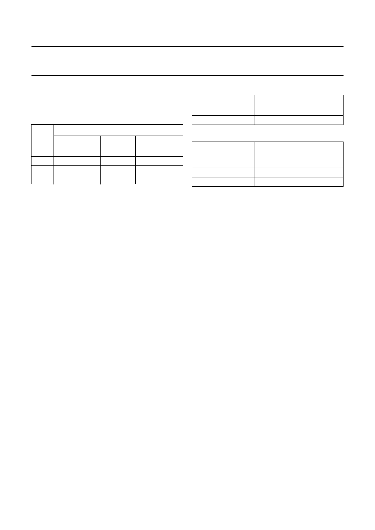
QUICK REFERENCE DATA
SYMBOL PARAMETER MIN. TYP. MAX. UNIT
f
i(RF)(RX)
f
o(RF)(TX)(GSM)
f
o(RF)(TX)(DCS)
f
IF
ORDERING INFORMATION
TYPE
NUMBER
UAA3522HL LQFP48 plastic low profile quad flat package; 48 leads; body 7 × 7 × 1.4 mm SOT313-2
GSM band RF input frequency in RX mode 925 − 960 MHz
GSM band RF output frequency in TX mode 880 − 915 MHz
DCS band RF output frequency in TX mode 1710 − 1785 MHz
IF frequency in all modes − 200 − MHz
PACKAGE
NAME DESCRIPTION VERSION
2000 Aug 15 3
This text is here in white to force landscape pages to be rotated correctly when browsing through the pdf in the Acrobat reader.This text is here in
h
_white to force landscape pages to be rotated correctly when browsing through the pdf in the Acrobat reader.This text is here inThis text is here in
white to force landscape pages to be rotated correctly when browsing through the pdf in the Acrobat reader. white to force landscape pages to be ...
2000 Aug 15 4
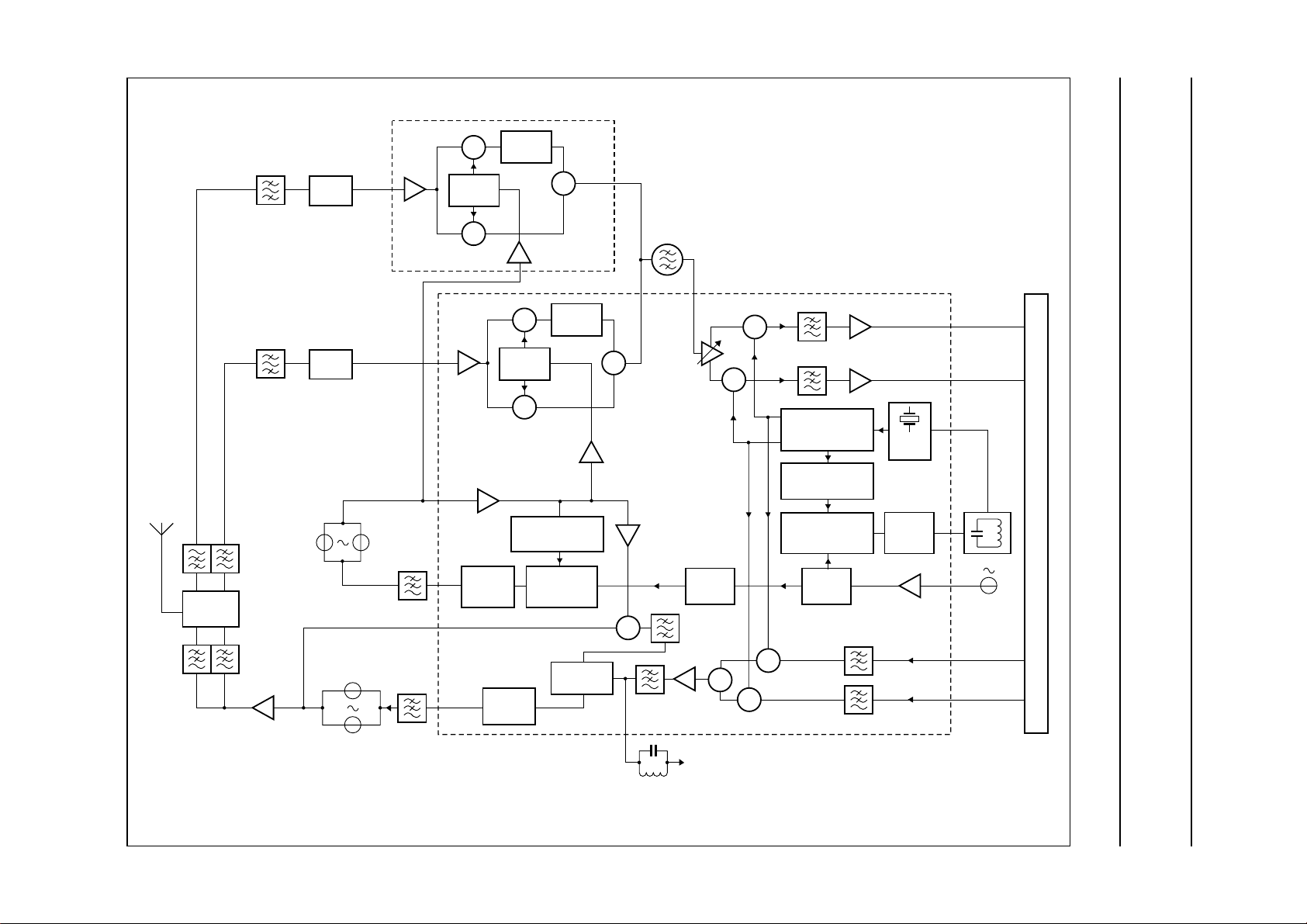
andbook, full pagewidth
BLOCK DIAGRAM
Philips Semiconductors Preliminary specification
Low power dual-band GSM transceiver
with an image rejecting front-end
RX/TX
SWITCH
1710 to 1785 MHz
DCS BAND
1805 to1880 MHz
925 to 960 MHz
DCS RF
RX VCO
1510 to 1680
MHz
880 to 915 MHz
GSM BAND
POWER
AMPLIFIER
BALUN
BALUN
1080 to 1160
GSM TX RF VCO
880 to 915 MHz
DCS TX RF VCO
1710 to 1785 MHz
UAA2077XM
GSM RF
RX VCO
MHz
90°
PHASE
SHIFTER
0°
41,
42
30, 31
26
38, 39
35
×
×
CHARGE
PUMP
CHARGE
PUMP
PHASE
SHIFTER
90°
+
PHASE
×
90°
PHASE
SHIFTER
0°
SHIFTER
×
PROGRAMMABLE
DIVIDER
RF PHASE/
FREQUENCY
DETECTOR
DETECTOR
ADDER
PHASE
90°
+
ADDER
UAA3522HL
×
44, 45
SAW
8, 946, 47
90°
DIVIDER
÷5
ADDER
+
4, 5
2, 3
13,
14
16
23
4, 5
2, 3
FCA004
I
Q
REF OSC.
13 MHz
I
Q
B
A
S
E
B
A
N
D
&
A
U
D
I
O
I
N
T
E
R
F
A
C
E
UAA3522HL
×
0°
IF VCO
400 MHz
×
DIVIDER &
PHASE
÷2
SHIFTER
PROGRAMMABLE
DIVIDER
IF PHASE/
FREQUENCY
DETECTOR
DIVIDER
÷13
0°
IF VCO
XTAL
CHARGE
PUMP
×
90°
×
Fig.1 Block diagram.
Philips Semiconductors Preliminary specification
Low power dual-band GSM transceiver
with an image rejecting front-end
PINNING
SYMBOL PIN DESCRIPTION
V
CCIF1
QA 2 Q path A baseband input/output
QB 3 Q path B baseband input/output
IA 4 I path A baseband input/output
IB 5 I path B baseband input/output
REFAGC 6 AGC reference resistor
GNDIF2 7 I/Q modulator and I/Q demodulator
RXIIFA 8 RX IF input A to AGC amplifier
RXIIFB 9 RX IF input B to AGC amplifier
V
CCIF2
TXON 11 TX mode control pin
V
CCIFLO
IFLOC 13 IF LO signal input from
IFLOE 14 IF LO signal input from
GNDIFLO 15 IF LO ground
CPOIF 16 IF charge pump output
GNDCPIF 17 IF charge pump and phase
V
CCCPIF
EN 19 serial programming bus enable
DATA 20 serial programming bus data input
CLK 21 serial programming bus clock input
GNDSYN 22 synthesizer ground
REFIN 23 13 MHz reference input
V
CCSYN
1 IF section of RF receiver supply
voltage 1
ground 2
10 I/Q modulator and I/Q demodulator
supply voltage 2
12 IF LO supply voltage
IF VCO resonator
IF VCO resonator
detector ground
18 IF charge pump and phase
detector supply voltage
control pin
24 synthesizer supply voltage
UAA3522HL
SYMBOL PIN DESCRIPTION
V
CCCPRF
CPORF 26 RF charge pump output
GNDCP 27 RF charge pump ground
SYNON 28 SYN mode control pin
V
CCRFLO
RFLOC 30 LO signal input from RF VCO
RFLOE 31 LO signal input from RF VCO
GNDRFLO 32 RF LO section ground
RXON 33 RX mode control pin
GNDPHD 34 transmit modulation loop charge
PHDOUT 35 charge pump output
V
CCPHD
RESEXT 37 reference resistor for transmit
TXIRFA 38 TX RF VCO signal input
TXIRFB 39 TX RF VCO signal input
V
CCRF
RXIRFA 41 RFreceiver input A
RXIRFB 42 RF receiver input B
GNDRF 43 RF receiver and transmit
TXIFA 44 transmit IFexternal filter A
TXIFB 45 transmit IFexternal filter B
RXOIFA 46 receiver IF output A
RXOIFB 47 receiver IF output B
GNDIF1 48 IF section of RF receiver ground 1
25 RF charge pump and phase
detector supply voltage
29 RF LO section supply voltage
pump ground
36 transmit modulation loop charge
pump supply voltage
modulation loop
40 RF receiver and transmit
modulation loop supply voltage
modulation loop ground
2000 Aug 15 5
Philips Semiconductors Preliminary specification
Low power dual-band GSM transceiver
with an image rejecting front-end
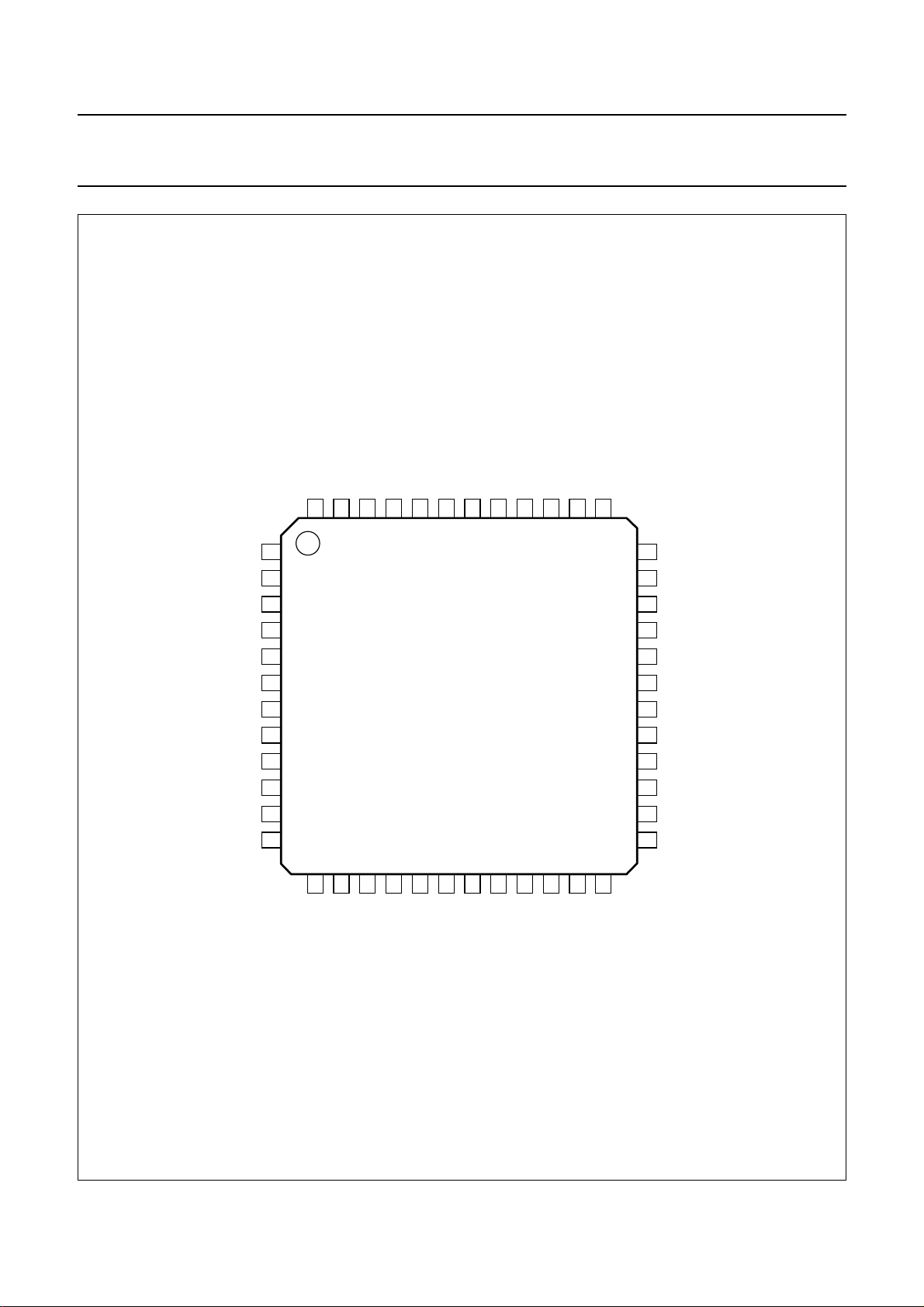
handbook, full pagewidth
GNDIF1
RXOIFB
RXOIFA
TXIFB
TXIFA
48
47
46
45
44
V
REFAGC
GNDIF2
V
V
CCIFLO
CCIF1
QA
QB
RXIIFA
RXIIFB
CCIF2
TXON
1
2
3
4
IA
5
IB
6
7
8
9
10
11
12
UAA3522HL
GNDRF
RXIRFB
43
42
RXIRFA
V
41
40
CCRF
TXIRFB
TXIRFA
39
38
RESEXT
37
V
36
35
PHDOUT
34
GNDPHD
33
RXON
32
GNDRFLO
31
RFLOE
30
RFLOC
V
29
28
SYNON
27
GNDCP
26
CPORF
V
25
UAA3522HL
CCPHD
CCRFLO
CCCPRF
13
14
15
16
17
18
IFLOE
IFLOC
CPOIF
GNDIFLO
CCCPIF
V
GNDCPIF
Fig.2 Pin configuration.
2000 Aug 15 6
19
EN
20
DATA
21
CLK
22
23
REFIN
GNDSYN
24
CCSYN
V
FCA043

Philips Semiconductors Preliminary specification
Low power dual-band GSM transceiver
with an image rejecting front-end
FUNCTIONAL DESCRIPTION
RF receiver
The receiver front-end convertsthe aerial RF signal, inthe
GSM band (925 to 960 MHz), to an IF signal of
approximately 200 MHz. The first stage of the receiver is
a symmetrical LNA that is matched to 50 Ω by an external
balun. The LNA is followed by an image rejection mixer
which suppresses the image by more than 30 dB.
It comprises two mixers in parallel driven by 0° and 90°
quadrature LO signals respectively. The IF signal from
one mixer is shifted by 90° with respect to the IF signal
from the other mixer, then both signals are added together
to cancel out the image signal. The resultant IF signal is
fed to the output via a high output impedance
open-collector stage which drives an external Surface
Acoustical Wave (SAW) filter which selects the required
channel.
I/Q demodulator
The signal from the SAW filter enters the I/Q demodulator
section. In addition to I/Q demodulation, this section
performs Automatic Gain Control (AGC) over a range of
60 dB to maintain a constant output level irrespective of
the antenna input level, and also applies additional
channel selectivity at the baseband stage using an
integrated high-order low-pass filter.
The AGC amplifier output can be adjusted for a static
offset of less than 50 mV. Its design prevents the offset
from varying by more than ±5 mV. To allow a more
accurateoffsetcalibration,theRF LNAcanbeswitchedoff
to ensure that no IF signal is present at the AGC amplifier
input during the offset measurement.
I/Q modulator
BasebandI and Q signalsareapplied to the I/Q modulator
whichshifts the modulation spectrum upto the transmit IF.
The I/Q modulator is designed for low harmonic distortion,
low carrier leakage and high image rejection to keep the
phase error as small as possible. Its IF output is loaded by
an integrated low-pass filter and by an external
LC tuned-circuit to prevent unwanted spurii from entering
the phase detector in the transmit modulation loop.
Transmit modulation loop
Theanalogtransmitmodulationloopcomprisesanon-chip
offset mixer and simple phase detector in switching mode
(triangular transfer function) forming an analog PLL with
an off-chip loop filter and transmit RF VCO.
UAA3522HL
The phase detector output transfers the modulation of the
I/Q IF signal to the off-chip transmit RF VCO making the
analog PLL act as a tracking filter. A PLL of at least
third-order is needed to meet noise requirements at
20 MHz offset from the carrier.
RF and IF LO sections
The active components required for the design of a low
noise IF VCO are provided on-chip. Pins IFLOC and
IFLOE connect the on-chip IF VCO components to an
external resonator and feedback circuit.
A divider and phase shifter divides the frequency of the
IF VCO signal by 2 and splits it into two signals having
phasesofrespectively0° and 90°whicharebothfedtothe
I/Q modulator and to the I/Q demodulator. The IF VCO
frequency is twice the IF to suppress the effects of
self-mixing and parasitic VCO modulation.
Pins TXIRFA and TXIRFAB connect an external receive
RF VCO module to the on-chip RF LO section. This
section includes a RC phase shifter which splits the
RF VCO signal into two signals having phases of
respectively 0° and 90° which are both fed to the
RX image rejection mixer.
Dual PLL
An on-chip high performance dual PLL synthesizes the
frequencies of the receive RF VCO and IF VCO signals.
Very low close-in phase noise is achieved which provides
a wide PLL bandwidth with a short settling time.
A dual programmable divider chain reduces the frequency
ofthereceiveRF and IF LO signalsto200 kHzand1 MHz
respectively.A digital phase/frequency detectorcompares
their phases to areference signal derived froman external
13 MHz clock signal. Phase error information is fed back
to both VCOs via the dual charge pump circuit which
adjusts the phase of each VCO signal by either ‘sinking’
current into, or ‘sourcing’ current from, its loop filter
capacitor, phase locking both RF and IF loops. The very
low leakage current of the dual charge pump circuit
ensures that any spurii are negligible.
Operating modes
BASIC OPERATING MODES
The circuit can be powered on in one of four operating
modesin which different partsof the device are enabled or
disabled. The four operating modes are called Idle, RX,
TX and SYN, and are selected by the hardware control
voltage level applied to pins RXON, TXON and SYNON.
2000 Aug 15 7
Philips Semiconductors Preliminary specification
Low power dual-band GSM transceiver
with an image rejecting front-end
The synthesizer, receiver and transmitter cannot all be on
at the same time. Table 1 shows which parts of the device
are enabled (on) or disabled (off) in each mode.
Table 1 Operating modes
POWER STATUS
MODE
SYNTHESIZER RECEIVER TRANSMITTER
Idle off off off
SYN on off off
RX on on off
TX on off on
The synthesizer includes the oscillators and LO buffers
commontothereceiveand transmit sections. The receiver
includes the RF section and the I/Q demodulator. When
the receiver is on, the LNA can be switched off to allow
DC offset compensation to be performed. The RF section
canalsobeswitchedoffforDCS applications.SeeSection
“Receiver power status control”.
RECEIVER POWER STATUS CONTROL
• DC offset compensation: This feature allows the
DC offset of the receiver output to be set accurately.
When the receiver is on, the LNA can be switched off to
isolate the antenna input from the I/Q demodulator
input. The offset at the I and Q outputs can be
independently reduced to less than 50 mV by
adequately programming two 5-bit data registers,
see Table 4 “Register bit allocation”. The LNA is
switched on or off by the status of bit LNA (see Table 2).
• Disabling RF section: For DCS applications, the RF
section can be disabled in RX mode. The same
IF circuits are used for both GSM and DCS applications
to avoid duplication. For DCS applications using the
UAA2077XM, for example, the RF section of the
UAA3522HL does not have to be powered on.
The RF section is enabled or disabled by the status of
bit RF when the RX mode is activated (see Table 3).
UAA3522HL
Table 2 Bit LNA status
BIT LNA STATUS POWER STATUS OF BIT LNA
0 off
1on
Table 3 Bit RF status
POWER STATUS OF
BIT RF STATUS
1 on (GSM)
0 off (DCS)
Programming
SERIAL PROGRAMMING BUS
A simple 3-wire unidirectional serial bus is used for
programming the IC. The lines are called DATA, CLK
and EN (enable). Programming data is sent to the IC in
bursts which are separated from each other by EN.
Programming clock edges are ignored until EN goes
activeLOW.Thedataisloadedintotheaddressedregister
when EN returns inactive HIGH, and when the CLK is in
either state, without affecting the data in the register.
The register only holds the last 18 bits that are serially
clocked into the IC.
Additional leading bits are ignored, and no check is made
on the number of clock pulses received. The fully static
CMOS design uses virtually no current when the bus is
inactive.It can always accept new programming dataeven
when both synthesizers are powered-off.
DATA FORMAT
Data is loaded into the register with the most significant bit
(MSB) first. The first 14 bits are data, while the last 4 bits
are the register address. The address bits are decoded on
the rising edge of EN. This internally generates a load
pulse to store the data in the addressed register.
To ensure that data loads correctly after the device has
powered-up,ENshouldbeheldLOWandonlytakenHIGH
after the appropriate register has been loaded.
The EN pulse is inhibited during the period when data is
read by the frequency dividers to prevent divider ratio data
from being read incorrectly. This state is guaranteed by
always allowing for a minimum EN pulse width after data
transfer.
RECEIVER RF SECTION
IN RX MODE
2000 Aug 15 8
2000 Aug 15 9
Table 4 Register bit allocation
X = don’t care; MSB = Most Significant Bit; LSB = Least Significant Bit.
DATA BITS ADDRESS BITS
Philips Semiconductors Preliminary specification
Low power dual-band GSM transceiver
with an image rejecting front-end
FIRST
BIT
LAST
BIT
13 12 11 10 9 8 7 6 5 4 3 2 1 0 3 2 1 0
X X X X X X MSB IF LO frequency divider ratio LSB 0 1 1 0
MSB RF LO frequency divider ratio LSB 0 1 0 0
XXXXX X LNA
(1)
X MSB AGC amplifier gain (RX mode)
LSB 0 0 1 1
see Table 5
X X MSB Q output offset adjust LSB Q sign
XXXXXIFRD
(3)
IF VCO
(4)
00RF
For test purposes only
(2)
MSB I output offset adjust LSB I sign
(5)
X SYN ON RX ON TX ON 0 0 0 1
(6)
(2)
001 0
000 0
Notes
1. Bit LNA: 1 = LNA ON in RX mode; 0 = LNA OFF in RX mode.
2. Bits Q sign and I sign = polarity of offset at Q/I channel outputs: 0 = negative offset step (output A with respect to output B); 1 = positive offset step
(output A with respect to output B).
3. Bit IF RD: 0 = frequency dividers programmed for GSM applications; 1 = frequency dividers programmed for DCS applications.
4. Bit IF VCO: 0 = IF LO buffer ON (external IF LO source connected); 1 = IF VCO ON (external IF LO source not connected).
5. Bit RF: 1 = RF section ON when RX mode is activated; 0 = RF section OFF when RX mode is activated.
6. This address must not be used. Data bits to be defined.
UAA3522HL
 Loading...