

Philips UAA3515AHL Datasheet

INTEGRATED CIRCUITS
DATA SH EET
UAA3515A
900 MHz analog cordless
telephone IC
Product specification
File under Integrated Circuits, IC17
2001 Dec 12

Philips Semiconductors Product specification
900 MHz analog cordless telephone IC UAA3515A
CONTENTS
1 FEATURES
1.1 Single frequency conversion FM receiver
1.2 Receiver baseband
1.3 Synthesizer
1.4 Transmitter
1.5 Transmitter baseband
1.6 Microcontroller interface
1.7 Power supplies
2 APPLICATIONS
3 GENERAL DESCRIPTION
4 ORDERING INFORMATION
5 BLOCK DIAGRAM
6 PINNING
7 FUNCTIONAL DESCRIPTION
7.1 Power supply and power management
7.1.1 Power supply
7.1.2 Power saving
7.1.3 Current consumption
7.2 FM receiver
7.2.1 Data comparator
7.3 Transmitter
7.4 Synthesizer
7.4.1 Calculation example
7.5 Receiver baseband
7.6 TX baseband
7.7 Voltage regulator
7.8 Low-battery detection
7.9 Microcontroller interface
7.9.1 Data registers
7.9.2 Active modes
7.9.3 Clock output divider
7.9.4 FM-PLL centre frequency
7.9.5 TX and RX gain control registers
7.9.6 Carrier detector threshold programming
7.9.7 Low-battery detection
7.9.8 Power amplifier output level
7.9.9 PLL charge pump current
7.9.10 Volume control
7.9.11 Crystal tuning capacitors
7.9.12 Voltage reference adjustment
7.9.13 Test mode
8 LIMITING VALUES
9 HANDLING
10 THERMAL CHARACTERISTICS
11 CHARACTERISTICS
12 PACKAGE OUTLINE
13 SOLDERING
13.1 Introduction to soldering surface mount
packages
13.2 Reflow soldering
13.3 Wave soldering
13.4 Manual soldering
13.5 Suitability of surface mount IC packages for
wave and reflow soldering methods
14 DATA SHEET STATUS
15 DEFINITIONS
16 DISCLAIMERS
2001 Dec 12 2

Philips Semiconductors Product specification
900 MHz analog cordless telephone IC UAA3515A
1 FEATURES
1.1 Single frequency conversion FM receiver
• Integrated Low Noise Amplifier (LNA)
• Image reject mixer
• FM detector (10.7 MHz) with:
– IF limiter
– wide band PLL demodulator
– output amplifier
– Received Signal Strength Indicator (RSSI) output
• Carrier Detector (CD) with programmable threshold
• Programmable data amplifier (slicer) phase.
1.2 Receiver baseband
• Programmable receiver gain
• Expander
• Earpiece amplifier with volume control feature
• Data amplifier.
1.3 Synthesizer
• Crystal reference oscillator with integrated tuning
capacitor
• Reference frequency divider
• Narrow band receiver PLL including VCO with
integrated variable capacitance diodes
• Narrow band transmitter PLL including VCO with
integrated variable capacitance diodes
• Integrated VCO circuits designed to function with
external inductors etched directly as part of the
printed-circuit board (cost-saving feature)
• Programmable clock divider with output buffer to drive
the microcontroller.
1.4 Transmitter
• Internal buffered Power Amplifier (PA) with
programmable gain
• Data transmission summing amplifier.
1.5 Transmitter baseband
• Programmable transmitter gain
• Microphone amplifier
• Compressor with Automatic Level Control (ALC) and
hard limiter.
1.6 Microcontroller interface
• Three-wire serial interface.
1.7 Power supplies
• Voltage regulator for internal PLL supplies
• Selectable voltage doubler
• Programmable Low-Battery Detection (LBD)
(time-multiplexed with RSSI carrier detector).
2 APPLICATIONS
• Analog cordless telephone sets (900 MHz).
3 GENERAL DESCRIPTION
The UAA3515A is a BiCMOS integrated circuit that
performs all functions from antenna to microcontroller in
reception and transmission for both base station and
handset ofa 900 MHz cordless telephone set. In addition,
the implemented programming reduces significantly the
amountofexternalcomponents,boardspaceandexternal
adjustments required.
4 ORDERING INFORMATION
TYPE
NUMBER
UAA3515AHL LQFP64 plastic, low profile quad flat package; 64 leads; body 10 × 10 × 1.4 mm SOT314-2
2001 Dec 12 3
NAME DESCRIPTION VERSION
PACKAGE

This text is here in white to force landscape pages to be rotated correctly when browsing through the pdf in the Acrobat reader.This text is here in
a
_white to force landscape pages to be rotated correctly when browsing through the pdf in the Acrobat reader.This text is here inThis text is here in
white to force landscape pages to be rotated correctly when browsing through the pdf in the Acrobat reader. white to force landscape pages to be ...
2001 Dec 12 4
ndbook, full pagewidth
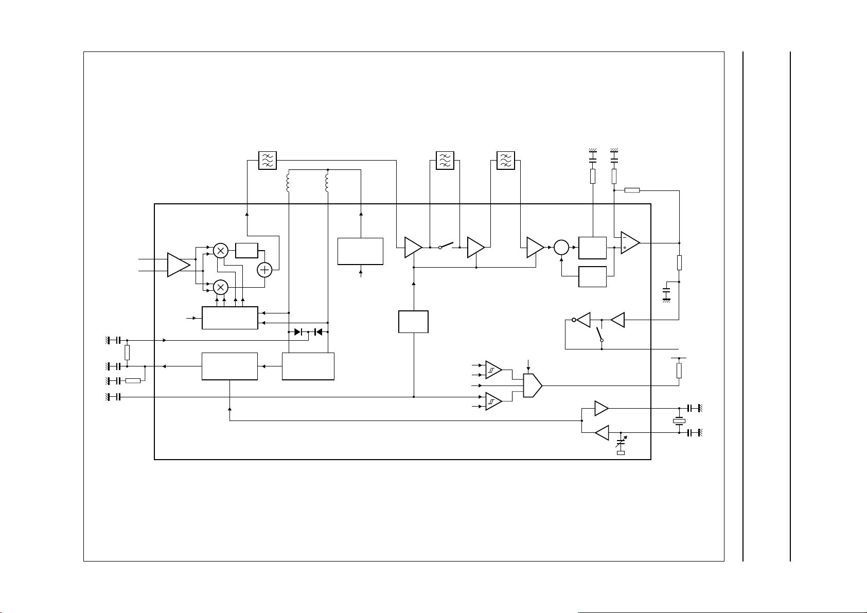
5 BLOCK DIAGRAM
Philips Semiconductors Product specification
900 MHz analog cordless telephone IC UAA3515A
IF 10.7 MHzIF 10.7 MHz
IF 10.7 MHz
V
CC(LNA)
64
1MIXGND
2RFIX
3RFIY
IMAGE
REJECTION
4LNAGND
FILTER
RXLF
5
V
CC(CP)
6
7
8
9
10
11CPGND
12
13
14
15PAGND1
16
RX
PHASE
DETECTOR
VOLTAGE
REGULATOR
V
CC(CP)
DETECTOR
RXPD
RSSI
V
REG
DGND
V
CC(CP)
V
CC(PS)
TXPD
V
CC
TXLF
PAO
MIXO
63
LNA
SBS
TX
PHASE
17
PAGND2
V
CC(MIX)
62
×
×
QUADRATURE
PHASE SHIFTER
10-BIT
MAIN RX
DIVIDER
VOLTAGE
REFERENCE
ADJUSTMENT
10-BIT
MAIN TX
DIVIDER
VB
mod
18
MODI
V
CC(BLO)
61
+
90
°
6-BIT
PRESCALER
PRESCALER
VB
19
MODO
VRXGND
60
+
RX
VOLTAGE
REFERENCE
6-BIT
TX
TX
VOLTAGE
REGULATOR
20
VTXGND
RXLOY58RXLOX
59
VCO RX
VB
COMPRESSOR
ALC
21
V
CC(VTX)
V
CC(VRX)
57
RX
VOLTAGE
REGULATOR
VB
UAA3515A
HARD
LIMITER
TX VCO
22
TXLOX23TXLOY
V
LFA1O
IFA1I
55
56
IF AMP 1 IF AMP 2 LIMITER
RSSI
RSSI
V
CC
VB
RSSI
VB
TX MUTE
24
V
CC(ATX)
IFA2I52LFA2O51IFGND50LIMI
CC(IF)
53
54
SFS
LBD
CD
V
TX GAIN
VB
25
26
CCAP
TXO
CD/LBD
CC(CP)
VOLTAGE
DOUBLER
CLOCK
DIVIDER
10-BIT
REFERENCE
DIVIDER
27
MICI
VD
en
MIC AMP
28
MICO
VCO
tune
DEMODULATOR
EXPANDER
VB
MICROCONTROLLER
VB
29
CMPI
PLLO
49
RX MUTE
R
EARPIECE
AMP
SERIAL
INTERFACE
31
30
VB
ATXGND32XTALI
Amp
RX GAIN
int
DATA AMP
48
47
46
45
44
43
42
41
40
39
38
37
36
35
34
33
DETO
LPFD
RXAI
ECAP
V
CC(ARX)
EARI
EARO
ARXGND
DATI
DATO
DATA
CLK
EN
CLKOUT
CDLBD
XTALO
FCA293
V
CC
V
CC
Fig.1 Block diagram.

Philips Semiconductors Product specification
900 MHz analog cordless telephone IC UAA3515A
6 PINNING
SYMBOL PIN DESCRIPTION
MIXGND 1 mixer ground
RFIX 2 LNA voltage (X) input
RFIY 3 LNA voltage (Y) input
LNAGND 4 LNA ground
RXLF 5 RX PLL filter output
RXPD 6 RX phase detector voltage output
RSSI 7 RSSI output
V
REG
DGND 9 digital ground
V
CC(CP)
CPGND 11 charge pump ground
V
CC(PS)
TXPD 13 TX phase detector voltage input
TXLF 14 TX PLL filter output
PAGND1 15 power amplifier ground 1
PAO 16 power amplifier output
PAGND2 17 power amplifier ground 2
MODI 18 summing amplifier input
MODO 19 summing amplifier output
VTXGND 20 transmitter VCO ground
V
CC(VTX)
TXLOX 22 transmitter VCO voltage (X) to external inductor
TXLOY 23 transmitter VCO voltage (Y) to external inductor
V
CC(ATX)
CCAP 25 external capacitor for compressor
TXO 26 audio transmitter output
MICI 27 microphone amplifier input
MICO 28 microphone amplifier output
CMPI 29 compressor input
VB 30 reference voltage
ATXGND 31 transmitter audio ground
XTALI 32 crystal input
XTALO 33 crystal output
CDLBD 34 CD or LBD open collector output (out-of-lock synthesizer receiver and/or
CLKOUT 35 clock output (CMOS levels)
EN 36 enable input for serial interface
CLK 37 clock input for serial interface
DATA 38 data input for serial interface
8 pin for internal voltage regulator
10 internal voltage doubler supply voltage (or positive supply voltage input) for
charge pumps
12 prescaler positive supply voltage input
21 transmitter VCO positive supply voltage input
24 transmitter audio positive supply voltage input
transmitter in test mode)
2001 Dec 12 5

Philips Semiconductors Product specification
900 MHz analog cordless telephone IC UAA3515A
SYMBOL PIN DESCRIPTION
DATO 39 data amplifier open collector output
DATI 40 data amplifier input
ARXGND 41 audio receiver ground
EARO 42 earpiece amplifier output
EARI 43 earpiece amplifier input
V
CC(ARX)
ECAP 45 external capacitor for expander
RXAI 46 audio receiver input
LPFD 47 demodulator loop filter output
DETO 48 demodulator amplifier output
PLLO 49 demodulator amplifier negative input
LIMI 50 limiter input
IFGND 51 IF negative supply voltage
IFA2O 52 IF second amplifier output
IFA2I 53 IF second amplifier input
V
CC(IF)
IFA1O 55 IF first amplifier output
IFA1I 56 IF first amplifier input
V
CC(VRX)
RXLOX 58 receiver VCO voltage (X) to external inductor
RXLOY 59 receiver VCO voltage (Y) to external inductor
VRXGND 60 receiver VCO ground
V
CC(BLO)
V
CC(MIX)
MIXO 63 mixer output
V
CC(LNA)
44 audio receiver positive supply voltage input
54 IF positive supply voltage input
57 receiver VCO positive supply voltage input
61 receiver LO buffer positive supply voltage input
62 mixers positive supply voltage input
64 LNA positive supply voltage input
2001 Dec 12 6
Philips Semiconductors Product specification
900 MHz analog cordless telephone IC UAA3515A
handbook, full pagewidth
CC(LNA)
V
64
MIXGND
LNAGND
V
CC(CP)
CPGND
V
CC(PS)
PAGND1
1
2
RFIX
3
RFIY
4
RXLF
5
RXPD
6
RSSI
7
V
8
REG
DGND
9
10
11
12
TXPD
13
TXLF
14
15
PAO 33
16
CC(MIX)VCC(BLO)
MIXO
V
63
62
61
VRXGND
RXLOY
60
59
CC(VRX)
RXLOX
V
IFA1I
58
57
56
UAA3515AHL
IFA1O
55
CC(IF)
V
54
IFA2I
53
IFA2O
52
IFGND
51
LIMI
50
PLLO
48
47
46
45
44
43
42
41
40
39
38
37
36
35
34
DETO
LPFD
RXAI
ECAP
V
CC(ARX)
EARI
EARO
ARXGND
DATI
DATO
DATA
CLK
EN
CLKOUT
CDLBD
XTALO
17
18
MODI
PAGND2
19
MODO
20
VTXGND
22
TXLOX
CC(VTX)
V
23
TXLOY
V
24
CC(ATX)
21
Fig.2 Pin configuration.
2001 Dec 12 7
25
CCAP
26
TXO
27
MICI
28
MICO
29
CMPI
30
VB
31
32
XTALI 49
ATXGND
FCA294
Philips Semiconductors Product specification
900 MHz analog cordless telephone IC UAA3515A
7 FUNCTIONAL DESCRIPTION
7.1 Power supply and power management
7.1.1 POWER SUPPLY
The UAA3515A is used in a cordless telephone handset
and in a base unit. The handset unit is battery powered
and operates on three NiCd cells. The minimum supply
voltage (VCC) is 2.9 V.
7.1.2 POWER SAVING
When the UAA3515A is used in a handset, it is important
to minimize current consumption. The main operating
modes are:
• Active mode (talk): all blocks are powered
• RX mode: all circuits in the receiver part are powered
Table 1 Power operating modes
CIRCUIT BLOCK ACTIVE MODE RX MODE INACTIVE MODE
Voltage reference adjustment power ON power ON power OFF
RF receiver power ON power ON power OFF
RX PLL power ON power ON power OFF
RX and TX audio paths power ON power OFF power OFF
RF TX (and PA, when enabled) power ON power OFF power OFF
• Inactive mode: with the exception of the microcontroller
interface, all circuits are powered-down. The crystal
reference oscillator, the output clock buffer, the voltage
regulator and the voltage doubler can be disabled
separately. To reduce microcontroller current
consumption, the crystal frequency to the clock output
canbedivided by 128. A low current consumption mode
for the crystal oscillator can be programmed.
Latch memory is maintained in all modes. Blocks that are
powered are shown in Table 1 per operating mode.
The crystal oscillator, the clock output buffer, the voltage
reference adjustment, the power amplifier, the voltage
doubler, the earpiece, the hard limiter and the ALC can be
activated separately. Blocks that can be activated in each
mode are shown in Table 2.
Table 2 Powered circuit blocks
CIRCUIT BLOCK ACTIVE MODE RX MODE INACTIVE MODE
Crystal oscillator; note 1 power ON power ON power ON
Clock output buffer power ON power ON power ON
Voltage reference enable; note 2 power ON power ON power ON
Power amplifier (PA2 = 1) power ON power OFF power OFF
Voltage doubler enable; note 3 power ON power ON power ON
Hard limiter and ALC not disabled power ON power OFF power OFF
Earpiece amplifier (earpiece enable = 1); note 4 power ON power ON power OFF
Notes
1. In RX and active mode, the crystal oscillator is activated automatically. An external frequency can be forced at the
crystal pins XTALI and XTALO.
2. In RX and active mode, the voltage reference is enabled automatically (whether bit V
3. If the voltage doubler is enabled, the crystal oscillator is activated automatically.
4. In inactive mode the amplifier is disabled automatically.
enable is logic 0 or 1).
REG
2001 Dec 12 8
Philips Semiconductors Product specification
900 MHz analog cordless telephone IC UAA3515A
7.1.3 CURRENT CONSUMPTION
The control bit values for selection of each mode and typical current consumption for the modes are shown in Table 3.
When clock out is activated there is an extra power demand proportional to the programmed output level (see Table 4
for examples). When bit Xtal high = 0 (oscillator is in low current consumption mode), the crystal in use must have losses
less than 20 Ω to ensure oscillator start-up.
Table 3 Typical current consumption
VCC= 3.3 V; T
amb
=25°C; f
= 10.24 MHz.
(i)xtal
POWER OPERATING MODE CONDITIONS
TYPICAL CURRENT
CONSUMPTION
Active mode 76 mA
RX mode 58 mA
Inactive mode xtal active = 0; V
xtal active = 1; V
xtal active = 1; V
xtal active = 1; V
xtal active = 1; V
enable = 0; note 1 <10 µA
REG
enable = 0; Xtal high = 0; note 1 230 µA
REG
enable = 0; Xtal high = 1; note 1 330 µA
REG
enable = 1; Xtal high = 1; note 1 550 µA
REG
enable = 1; Xtal high = 0; note 2 690 µA
REG
Notes
1. Voltage doubler and clock output buffer disabled.
2. Voltage doubler enabled, clock output buffer disabled.
Table 4 Examples of additional current consumption
V
= 3.3 V; T
CC
amb
=25°C; f
= 10.24 MHz; C
(i)xtal
L(CLKOUT)
=14pF.
CURRENT CONSUMPTION ADDITIONAL TO TYPICAL VALUE
DIVIDER RATIO
CLKO level = 0 CLKO level = 1
1, 2, 2.5, 4 or 128 770 µA 530 µA
off 0 0
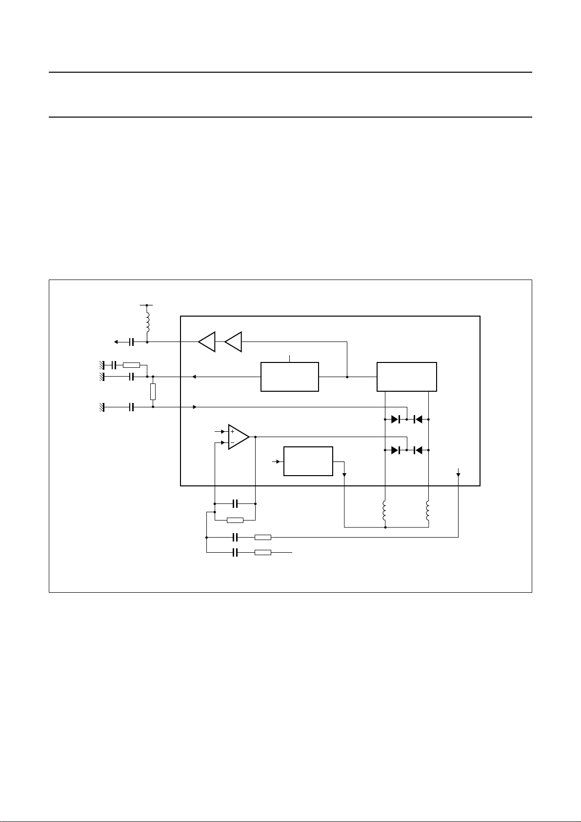
7.2 FM receiver
The FM receiver (see Fig.3) has a single frequency conversion architecture with integrated image rejection mixer that
makes an external RF filter unnecessary. The Side Band Select (SBS) feature allows choice of frequency for RXLO to
be in or out of the ISM band allowing use of the same IC type for both base station and handset. IF channel filtering
(a compromise between price and performance) can be implemented simply using two or three external 10.7 MHz filters.
The integrated FM PLL demodulator with limiter decreases significantly the number of pins and external components
required.
2001 Dec 12 9
This text is here in white to force landscape pages to be rotated correctly when browsing through the pdf in the Acrobat reader.This text is here in
_white to force landscape pages to be rotated correctly when browsing through the pdf in the Acrobat reader.This text is here inThis text is here in
white to force landscape pages to be rotated correctly when browsing through the pdf in the Acrobat reader. white to force landscape pages to be ...
2001 Dec 12 10
handbook, full pagewidth
Philips Semiconductors Product specification
900 MHz analog cordless telephone IC UAA3515A
RXPD
IF 10.7 MHzIF 10.7 MHz
MIXO
63
+
90
2RFIX
LNA
3RFIY
SBS
5RXLF
6
7RSSI
QUADRATURE
PHASE SHIFTER
DUAL PLL
FREQUENCY
SYNTHESIZER
°
RXLOY58RXLOX
59
VCO RX
V
CC(VRX)
57
VOLTAGE
REGULATOR
VB
IFA1I
56
IFA1O
55
IF AMP 1 IF AMP 2 LIMITER
RSSI
SFS
V
OL RX/TX
IF 10.7 MHz
IFA2I52IFA2O50LIMI
53
UAA3515A
CD/LBD
CC
VB
VB
LBD
CD
PLLO
LPFD
49
47
AMP
DETO
DATA AMP
48
40
39
34
33
32
DATI
DATO
CDLBD
XTALO
XTALI
V
CC
LOOP
×
FILTER
VCO
Fig.3 FM receiver block diagram.
FCA295
Philips Semiconductors Product specification
900 MHz analog cordless telephone IC UAA3515A
7.2.1 DATA COMPARATOR
The data comparator is an inverting hysteresis
comparator. An external bandpass filter is connected
between pins DETO and DATI (AC-coupled). The
open-collectoroutputiscurrent limited to controltheoutput
signal slew rate. An external resistor of 180 kΩ should be
connected between pin DATO and VCC. An external
capacitor in parallel with this resistor will reduce the slew
rate.
V
C
CC
L
P
16PAO
S
DUAL PLL
FREQUENCY
SYNTHESIZER
SUMMING
TXLF
13TXPD
14
VB
mod
AMPLIFIER
handbook, full pagewidth
7.3 Transmitter
The transmitter architecture is of the direct modulation
type. The transmit VCO can be frequency modulated by
speech or data (see Fig.4). An amplifier sums the
modulating signal with the data TX signal before the VCO.
Frequency control is affected by integrated variable
capacitance diodes. To obtain the correct frequency,
external inductors in series with the bonding wires and
leadframe are required. The power amplifier is capable of
driving a 50 Ω load. The level of the output signal PAO is
programmed with two bits via the serial bus interface.
UAA3515A
XTAL
TX VCO
TX
VOLTAGE
REGULATOR
Data TX
18
MODI
VB
19
MODO
Fig.4 Transmitter block diagram.
21
V
CC(VTX)
22
TXLOX
23
TXLOY26TXO
FCA296
2001 Dec 12 11

Philips Semiconductors Product specification
900 MHz analog cordless telephone IC UAA3515A
7.4 Synthesizer
The crystal local oscillator and reference divider (see
Fig.5) provide the reference frequency for the RX and TX
PLLs. The 10-bit reference divider is programmed with
respect to the crystal frequency and the desired RX and
TX frequencies. The microcontroller operating frequency
of 4.096 MHz is derived from a 16.384 MHz crystal
frequency. The clock divider ratio can be programmed to
1, 2, 2.5, 4 or to 128; ratio 128 is chosen in sleep mode to
save current in the microcontroller section. Clock output
(pin CLKOUT) is an emitter follower output.
The 16-bit TX counter is programmed for the desired
transmit channel frequency. Similarly, the 16-bit RX
counter is programmed for the desired local oscillator
frequency.Thedividercounter comprises a 6-bit prescaler
with division ratios (R) from 64 to 127, and a 10-bit CMOS
divider with division ratios (C) from 8 to 1023. The full
counter provides division ratios from 512 to 65535.
Settings of RX and TX counters are calculated as follows:
C = int
M
-----64
R=M−C×64
(where M is the division ratio between VCO frequency and
the reference frequency).
7.4.1 CALCULATION EXAMPLE
Given:
RF input frequency f
VCO RX f
VCO(RX)
= 892.3 MHz
= 903 MHz
i(RF)
fIF= 10.7 MHz
VCO TX f
VCO(TX)
= 925.6 MHz
Internal comparison frequency = 20 kHz
(f
= 10.24 MHz)
XTAL
We have:
Reference divider = 512 (1000000000)
6
×
MRX
892.3 10
------------------------------
44615==
20 103×
C RX = 697 (1010111001) and R RX = 7 (000111)
and
MTX
925.6 106×
------------------------------
46280==
20 103×
C TX = 723 (1011010011) and R TX = 8 (001000)
VCOs and variable capacitance diodes are integrated.
Resonance inductors are shared between bonding wires,
leadframe of the package and external inductors. Costs
can be reduced by etching external inductors directly onto
the printed-circuit board.
An on-chip selectable voltage doubler is provided to
enable a larger tuning range of both VCOs. The phase
detectors have current drive type outputs with selection
possibilities between 400 and 800 µA.
2001 Dec 12 12

This text is here in white to force landscape pages to be rotated correctly when browsing through the pdf in the Acrobat reader.This text is here in
a
_white to force landscape pages to be rotated correctly when browsing through the pdf in the Acrobat reader.This text is here inThis text is here in
white to force landscape pages to be rotated correctly when browsing through the pdf in the Acrobat reader. white to force landscape pages to be ...
2001 Dec 12 13
ndbook, full pagewidth
Philips Semiconductors Product specification
900 MHz analog cordless telephone IC UAA3515A
RXPD
TXLF
5RXLF
6
13TXPD
14
V
CC(CP)
RX
PHASE
DETECTOR
V
CC(CP)
TX
PHASE
DETECTOR
VB
10-BIT
MAIN RX
DIVIDER
10-BIT
MAIN TX
DIVIDER
TX
VOLTAGE
REGULATOR
6-BIT
PRESCALER
RX
6-BIT
PRESCALER
TX
MODO
21
V
CC(VTX)
RXLOY
59
VCO RX
TX VCO
22
TXLOX
RXLOX
58
23
TXLOY
V
CC(VRX)
57 10
RX
VOLTAGE
REGULATOR
VB
UAA3515A
V
CC(CP)
VD
VOLTAGE
DOUBLER
CLOCK
DIVIDER
10-BIT
REFERENCE
DIVIDER
en
CLKOUT
35
XTALO
33
XTALI
32
FCA297
Fig.5 Synthesizer block diagram.
Philips Semiconductors Product specification
900 MHz analog cordless telephone IC UAA3515A
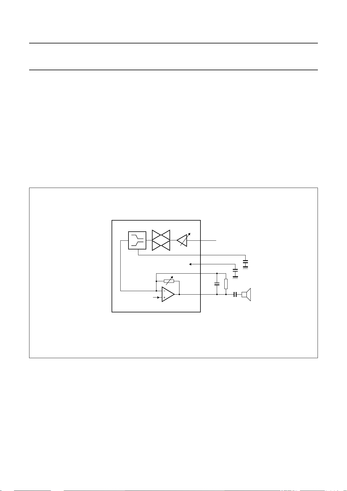
7.5 Receiver baseband
This section covers the RX audio path from pins RXAI to
EARO (see Fig.6). The RXAI input signal is AC-coupled.
The microcontroller sets the value of the RX gain in
32 linear steps of 0.5 dB. The RX baseband has a mute
function and an expander with characteristics as shown in
Fig.7.
For audio level adjustment and, potentially for software
volume control, setting the RX gain provides a dynamic
range of 31 dB. This is achieved by the expander slope
that multiplies the RX gain by a factor of two for each gain
step thus giving 1 dB steps measured at the earpiece
amplifier output.
handbook, full pagewidth
EXPANDER
RX MUTE
The earpiece amplifier is a rail-to-rail inverting operational
amplifier. The non-inverting input is connected to the
internal reference voltage at pin VB. Software volume
control on the earpiece amplifier is achieved by using an
integrated switched feedback resistor R
. The volume
int
control tuning range is 14 dB. Hardware volume control is
achieved by switching externally the earpiece feedback
resistor R
RX GAIN
.
ext
RXAI
46
R
int
VB
UAA3515A
EARPIECE
AMPLIFIER
FCA298
Fig.6 RX baseband block diagram.
45
44
43
42
ECAP
V
CC(ARX)
EARI
C
ext
EARO
R
ext
2001 Dec 12 14
 Loading...