

Philips UAA3500HL Datasheet

INTEGRATED CIRCUITS
DATA SH EET
UAA3500HL
Pager receiver
Objective specification
File under Integrated Circuits, IC17
1999 Mar 30
Philips Semiconductors Objective specification
Pager receiver UAA3500HL
FEATURES
• Double frequency conversion, zero-IF receiver with:
– Configurable in all paging bands (130 to 930 MHz)
– Low noise amplifier featured with four step Automatic
Gain Control (AGC)
– Down-conversion mixers
– On-chip, zero-IF channel filter
– I/Q, non-demodulated outputs
– Highpass filters to remove DC offsets.
• External Voltage Controlled Oscillator (VCO).
– Both LOs derived from the VCO.
APPLICATIONS
• FLEX, ERMES and POCSAG pagers
• Remote control terminals.
GENERAL DESCRIPTION
The UAA3500HL is a one-chip pager receiver complying
with POCSAG, FLEX and ERMES standards.
The IC performs in accordance with specifications in the
−10 to +55 °C temperature range.
The UAA3500HL contains a front-end receiver
configurable, through external components, for any
frequency band between 130 and 930 MHz. The back-end
receiver consists of the channel filter and limiters.
An external VCO ensures the Local Oscillator (LO) for the
front-end. Designed in an advanced BiCMOS process, it
combines high performance with low-power consumption
and a high degree of integration, thus reducing external
component costs and total radio size.
Its first advantage is to remove the expensive SAW filter
necessary in a superhet architecture and to replace it by
an integrated, elliptic channel filter that provides 70 dB
adjacent channel rejection. The receive front-end section
consists of a low-noise amplifier that drives mixers through
an external LC image rejection filter. The output drives the
I and Q second mixers, whose outputs are at zero
frequency. The receiver back-end section consists of
filters (channel filtering), limiters (limited output required)
and high-pass filters (DC-block) to remove DC offsets.
Outputs are I and Q, undemodulated signals.
Its second advantage is to provide the two LO signals only
from one VCO tuned by a PLL. On-chip frequency
divider-by-2 and buffers provide the LO sources.
Its third advantage is to provide two voltage regulators,
allowing to obtain 1.0 and 1.8 V regulated voltages.
ORDERING INFORMATION
TYPE NUMBER
NAME DESCRIPTION VERSION
UAA3500HL LQFP48 plastic low profile quad flat package; 48 leads; body 7 × 7 × 1.4 mm SOT313-2
PACKAGE
1999 Mar 30 2
Philips Semiconductors Objective specification
Pager receiver UAA3500HL
QUICK REFERENCE DATA
SYMBOL PARAMETER CONDITIONS
V
CC1
V
CC2
I
CC1(RX)
supply voltage 1 (B++) 1.85 2.1 3.3 V
supply voltage 2 (B+) 1.05 1.4 1.5 V
receive supply current from B++ 160 MHz − 2.4 − mA
(1)
MIN. TYP. MAX. UNIT
280 MHz − 2.4 − mA
930 MHz − 2.5 − mA
I
CC2(RX)
receive supply current from B+ 160 MHz − 1.3 − mA
280 MHz − 1.4 − mA
930 MHz − 2.3 − mA
NF
RX
receiver noise figure 160 MHz − 2.7 − dB
280 MHz − 3.1 − dB
930 MHz − 4.4 − dB
Sens sensitivity; 3% BER and 1600 bits/s
2 level
160 MHz −−128.5 − dBm
280 MHz −−128 − dBm
930 MHz; note 2 −−126.5 − dBm
ACR adjacent channel rejection 65 70 − dB
T
amb
operating ambient temperature −10 +25 +55 °C
Notes
1. For 930 MHz band; for other conditions see Chapters “DC characteristics” and “AC characteristics”.
2. Sensitivity; 3% BER and 6400 bits/s 4 level: −123 dBm.
1999 Mar 30 3
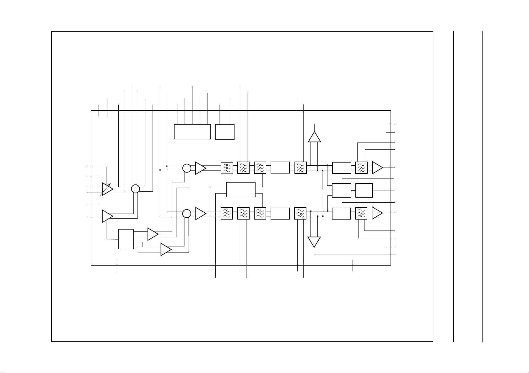
This text is here in white to force landscape pages to be rotated correctly when browsing through the pdf in the Acrobat reader.This text is here in
h
_white to force landscape pages to be rotated correctly when browsing through the pdf in the Acrobat reader.This text is here inThis text is here in
white to force landscape pages to be rotated correctly when browsing through the pdf in the Acrobat reader. white to force landscape pages to be ...
1999 Mar 30 4
V
CC(DC
)
DRV2
)
V
CC(LO
CAPI1A
)
FASTON
RXON
M1GND
M2GND
IMINA
IMOUTA
IMINB
IMOUTB
FILINA
FILOUTA
FILINB
FILOUTB
V
DRV1
CC(FE
andbook, full pagewidth
CAPI1B
CAPI2A
CAPI2B
BLOCK DIAGRAM
Pager receiver UAA3500HL
Philips Semiconductors Objective specification
RSET
LNAGND2
RFINA
RFINB
LNAGND1
LOIN
4037
33
32
LNA
31
30
29
BUFFER
21
2
22 14 13 20 19 10 9 48
LOGND
42 41 46 47 16 17 18 25 24 28 23 43 44 3 4
39383635
VOLTAGE
REGULATOR
PMA
BIAS
×
×
GYRATOR
REGULATOR
×
BUFFER
0
90
BUFFER
PMA
GYRCO1
GYRCO2
UAA3500HL
CAPQ1B
LIMITER
LIMITER
CAPQ2ACAPQ1A
CAPQ2B
BUFFER
BUFFER
LIMITER
AGC
LIMITER
BEGND
RSSI
OUTPUT
OUTPUT
45
5
2
1
6
26
34
27
7
11
12
8
15
GYROUTI
V
CC(O)
CAPI3A
CAPI3B
OUTI
AGCADJ
RSSI
AGCTAU
OUTQ
CAPQ3A
CAPQ3B
OGND
GYROUTQ
FCA022
Fig.1 Block diagram.
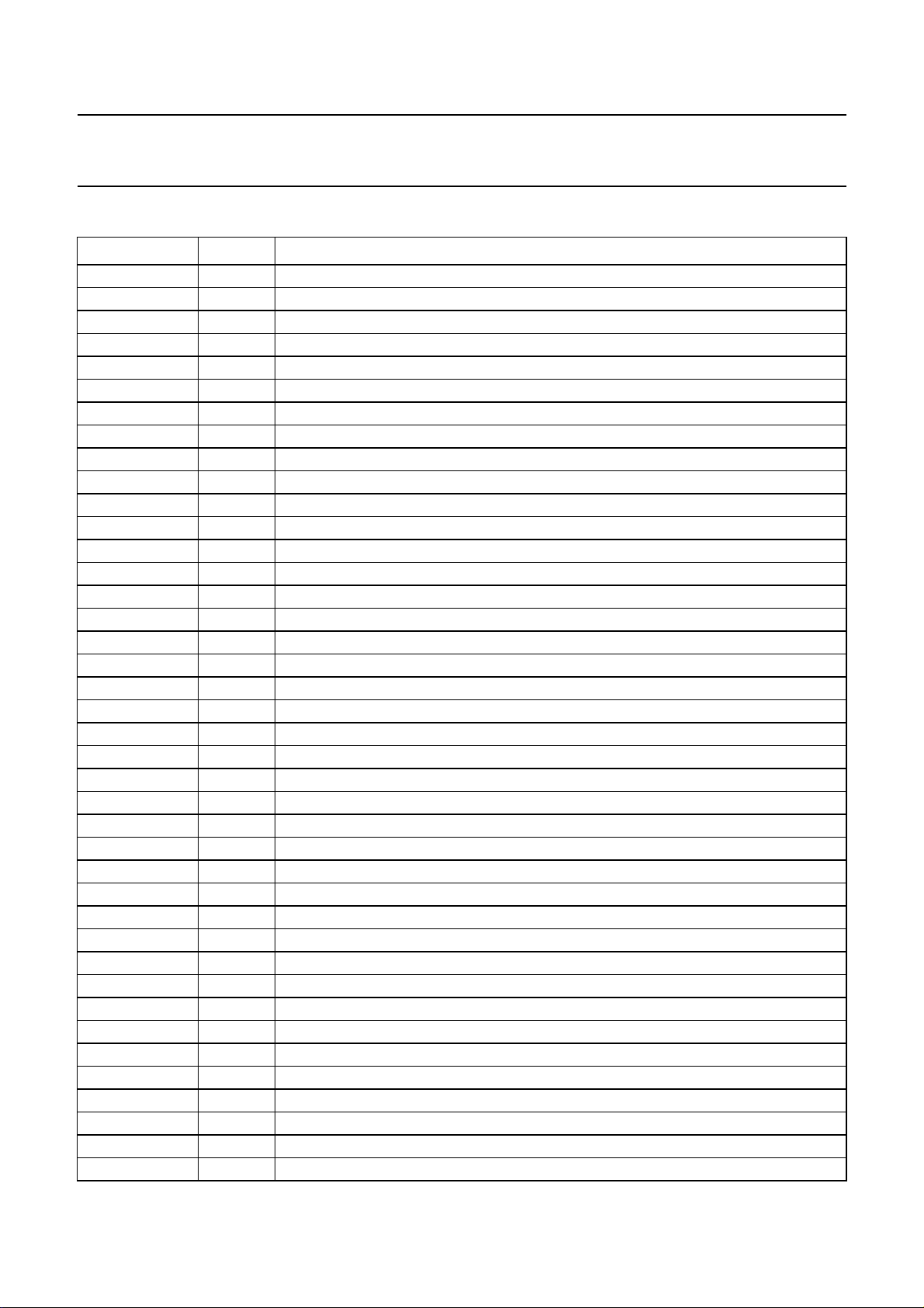
Philips Semiconductors Objective specification
Pager receiver UAA3500HL
PINNING
SYMBOL PIN DESCRIPTION
CAPI3B 1 3rd DC filter (I path) external capacitor B (I path)
CAPI3A 2 3rd DC filter (I path) external capacitor A (I path)
CAPI2A 3 2nd DC filter (I path) external capacitor A (I path)
CAPI2B 4 2nd DC filter (I path) external capacitor A (I path)
V
CC(O)
OUTI 6 output I and Q signals (I path)
OUTQ 7 output I and Q signals (Q path)
OGND 8 output stage ground
CAPQ2B 9 2nd DC filter external capacitor B (Q path)
CAPQ2A 10 2nd DC filter external capacitor A (Q path)
CAPQ3A 11 3rd DC filter external capacitor A (Q path)
CAPQ3B 12 3rd DC filter external capacitor B (Q path)
GYRCO2 13 external resistor to set-up gyrator filter cut-off frequency
GYRCO1 14 external resistor to set-up gyrator filter cut-off frequency
GYROUTQ 15 Q-gyrator output
DRV1 16 regulator driver (1.8 V)
V
CC(FE)
V
CC(DC)
CAPQ1B 19 1st DC filter external capacitor (Q path)
CAPQ1A 20 1st DC filter external capacitor (Q path)
LOIN 21 LO input
LOGND 22 LO strip ground
FASTON 23 fast mode enable
V
CC(LO)
DRV2 25 regulator driver (1.0)
AGCADJ 26 AGC loop gain control
AGCTAU 27 AGC loop time constant
RXON 28 receiver mode enable
LNAGND1 29 receiver LNA ground 1
RFINB 30 LNA input B
RFINA 31 LNA input A
LNAGND2 32 receiver LNA ground 2
RSET 33 LNA current setup
RSSI 34 received signal strength indicator
IMINA 35 image rejection filter input A
IMINB 36 image rejection filter input B
M1GND 37 first mixer ground
IMOUTA 38 image rejection filter output A
IMOUTB 39 image rejection filter output B
M2GND 40 second mixers ground
5 output stage supply voltage B (I path)
17 regulated voltage for front-end (1.8 V)
18 input voltage from DC-to-DC converter (2.1 V)
24 regulated voltage for LO strip (1.0 V)
1999 Mar 30 5
 Loading...