

Philips UAA3202M Datasheet

INTEGRATED CIRCUITS
DATA SH EET
UAA3202M
Frequency Shift Keying (FSK)
receiver
Preliminary specification
File under Integrated Circuits, IC01
1997 Aug 12

Philips Semiconductors Preliminary specification
Frequency Shift Keying (FSK) receiver UAA3202M
FEATURES
• Low cost single-chip FSK receiver
• Superheterodyne architecture with high integration level
• Few external low cost components
• Wide supply voltage range
• Low power consumption
• Wide frequency range, 150 to 450 MHz
• High sensitivity
• IF band determined by application
• High selectivity
• Very low spurious radiation, −60 dBm
(meets FTZ 17TR2100)
• Automotive temperature range
• Power-down mode
• SSOP20 package.
Applications
• Keyless entry systems
• Car alarm systems
• Remote control systems
• Security systems
• Telemetry systems
• Wireless data transmission
• Domestic appliances.
GENERAL DESCRIPTION
The UAA3202M is a fully integrated single-chip receiver,
primarily intended for use in VHF and UHF systems
employing direct Frequency Shift Keying (FSK)
modulation. The UAA3202M incorporates a SAW
stabilized local oscillator, balanced mixer, IF amplifier,
limiter, Received Signal Strength Indicator (RSSI), RSSI
comparator, FSK demodulator, data filter and data slicer.
The device features a power-down mode in order to
minimize the average receiver supply current.
QUICK REFERENCE DATA
SYMBOL PARAMETER CONDITIONS MIN. TYP. MAX. UNIT
V
CC
I
CC
P
sens
supply voltage 3.5 − 6V
supply current for
operating mode on V
operating mode off V
sensitivity fi= 433.92 MHz;
=0V; R2= 560 Ω 2.0 3.4 4.7 mA
PWD
PWD=VCC
− 330µA
−−−94 dBm
f
= 250 Hz square wave;
mod
∆f=±25 kHz; BER ≤ 3%
T
amb
operating ambient temperature −40 − +85 °C
ORDERING INFORMATION
TYPE
NUMBER
NAME DESCRIPTION VERSION
UAA3202M SSOP20
plastic shrink small outline package; 20 leads; body width 5.3 mm
PACKAGE
SOT339-1
1997 Aug 12 2
Philips Semiconductors Preliminary specification
Frequency Shift Keying (FSK) receiver UAA3202M
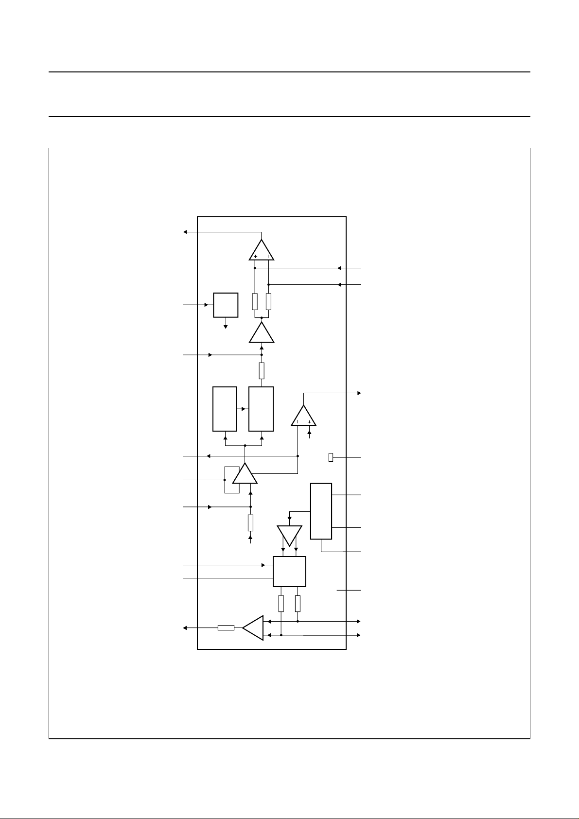
BLOCK DIAGRAM
MHA797
150 kΩ
BIAS
ref
V
150 kΩ
BUFFER
UAA3202M
EM MXIN LIN RSSI DMODLFB CPC PWD DATA
V
FA
30 kΩ
COMP CPB CPA
SHIFT
PHASE
PHASE
DETECTOR
ref
V
RSSI
EE
V
Fig.1 Block diagram.
EO
LIMITER
AMPLIFIER
50 kΩ
CC
V
MIXER
IF
1.4 kΩ
20 19 18 17 16 15 14 13 12 11
AMP
1.5 kΩ
1.5 kΩ
OSCILLATOR
OSC OSE V
CC
12 3 4 5 6 7 8 9 10
MON MOP V
handbook, full pagewidth
1997 Aug 12 3
Philips Semiconductors Preliminary specification
Frequency Shift Keying (FSK) receiver UAA3202M
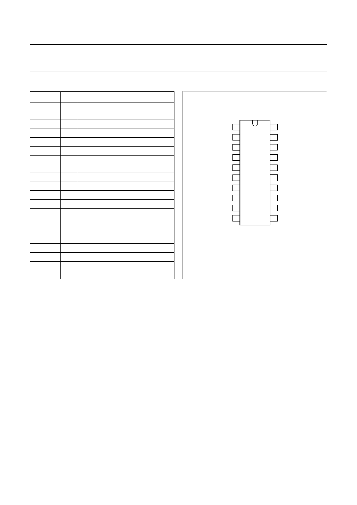
PINNING
SYMBOL PIN DESCRIPTION
MON 1 negative mixer output
MOP 2 positive mixer output
V
CC
3 positive supply voltage
OSC 4 oscillator collector
OSE 5 oscillator emitter
V
EO
V
EE
6 negative supply voltage for oscillator
7 negative supply voltage
COMP 8 RSSI comparator output
CPB 9 comparator input B
CPA 10 comparator input A
DATA 11 data output
PWD 12 power-down control input
CPC 13 comparator input C
DMOD 14 demodulator frequency adjustment
RSSI 15 RSSI current output
LFB 16 limiter feedback
LIN 17 limiter input
MXIN 18 mixer input
V
EM
19 negative supply voltage for mixer
FA 20 IF amplifier output
handbook, halfpage
MON
1
MOP
2
V
3
CC
OSC
4
OSE
5
EO
EE
UAA3202M
6
7
8
9
10
MHA796
V
V
COMP
CPB
CPA
Fig.2 Pin configuration.
20
19
18
17
16
15
14
13
12
11
FA
V
EM
MXIN
LIN
LFB
RSSI
DMOD
CPC
PWD
DATA
1997 Aug 12 4

Philips Semiconductors Preliminary specification
Frequency Shift Keying (FSK) receiver UAA3202M
FUNCTIONAL DESCRIPTION
The device is based on the superheterodyne architecture
incorporating a mixer, local oscillator, IF amplifier, limiter,
RSSI, RSSI comparator, FSK demodulator, data filter,
data slicer and power-down circuitry. The device employs
a low IF frequency of typically 1 MHz in order to allow IF
filtering by means of external low cost R, L and C
components. If image rejection is required it can be
achieved by applying a matching external front-end SAW
filter. The device provides a wide IF range of 300 kHz in
order to allow the use of a SAW stabilized oscillator.
The on-chip local oscillator provides the injection signal for
the mixer. Tuning of the on-chip local oscillator is not
necessary. The oscillator frequency is determined by an
external 1-port SAW resonator. The RF input signal is fed
to the mixer and down converted to the IF frequency. After
amplification and filtering the RF signal is applied to a
limiter. The IF filter order and characteristics are
determined by the external low cost R, L and C
components. The limiter amplifier provides a RSSI signal
which can be routed to an on-chip RSSI level comparator
in order to derive a field strength indication for external
use. The limited IF signal is fed to the FSK demodulator.
The demodulator centre frequency is determined by an
external capacitor. No alignment is necessary for the FSK
demodulator. After filtering the demodulated data signal is
fed to a data slicer and is made available at the data
output. The data filter characteristics are determined by
external capacitors. The data slicer employs an adaptive
slice reference in order to track frequency offsets.
The device is switched from power-down to operating
mode and vice versa by means of a control input.
Extremely low supply current is drawn when the device is
in power-down mode. Measures are taken to allow fast
receiver settling when the device is switched from
power-down to operating mode.
Mixer
Post mixer amplifier
The Post Mixer Amplifier (PMA) is a differential input,
single-ended output amplifier. It separates the first and
second IF filters from each other. Amplifier gain is provided
in order to reduce the influence of the limiter noise figure
on the total noise figure.
Limiter
The limiter is a single-ended input multiple stage amplifier
with high total gain. Amplifier stability is achieved by
means of an external DC feedback capacitor, which is also
used to determine the lower limiter cut-off frequency.
An RSSI signal proportional to the limiter input signal is
provided.
IF filters
IF filtering with high selectivity is realized by means of
external low cost R, L and C components. The first IF filter
is located directly following the mixer output. An external
L/C network assembles a band-pass with low sensitivity in
order to meet the bandwidth of an elliptic low-pass filter
external to the device and is located in front of the limiter.
The filter source impedance is determined by the drive
impedance of the IF amplifier. In order to improve the IF
filter selectivity below the pass-band a high-pass
characteristic is added by means of a DC blocking
capacitor in front of the limiter input and by means of the
limiter DC feedback capacitor.
RSSI
The RSSI signal is a current proportional to the limiter input
level (RF input power). By means of an external resistor
the resulting RSSI voltage level is set in order to fit the
application. The RSSI voltage is available to external
circuits and is fed to the input of the RSSI level
comparator. For RSSI filtering an external capacitor is
connected.
The mixer is a single balanced emitter coupled mixer with
internal biasing. Matching of the RF source impedance to
the mixer input requires an external matching network.
Oscillator
The oscillator consists of an on-chip transistor in common
base configuration. An external tank and SAW resonator
determines the oscillator frequency. Oscillator alignment is
not necessary. Oscillator bias is controlled by an external
resistor.
1997 Aug 12 5
RSSI level comparator
The RSSI level comparator compares the RSSI level with
a fixed and independent internal reference voltage. If the
RSSI level exceeds the internal reference voltage a logic
HIGH signal is generated. The level comparator provides
some hysteresis in order to avoid spurious oscillation.
The output of the level comparator is designed as an
open-collector with internal pull-up.

Philips Semiconductors Preliminary specification
Frequency Shift Keying (FSK) receiver UAA3202M
FSK demodulator
The limited IF signal is converted into baseband data by
means of a quadrature FM demodulator consisting of an
all-pass filter and a mixer stage. No alignment of the
demodulator is necessary. The demodulator centre
frequency is set by a capacitor external to the device.
The demodulator provides a large audio bandwidth in
order to allow high data rate applications.
The demodulator can detect a small IF frequency deviation
even if a relatively large IF frequency offset is
encountered.
Data filters
After demodulation a two-stage data filtering circuit is
provided in order to suppress unwanted frequency
components. Two R/C low-pass filters with on-chip
resistors are provided which are separated by a buffer
stage.
Data slicer
Data detection is provided by means of a level comparator
with adaptive slice reference. After the first data filter stage
the pre-filtered data is split into two parts. One part passes
the second data filter stage and is fed to the positive
comparator input.
The other path is fed to an integration circuit with a large
time constant in order to derive the average value
(DC component) as an adaptive slice reference which is
presented to the negative comparator input. The adaptive
reference enables the received data over a large range of
demodulator frequency offsets to be detected.
The integration circuit consists of a simple R/C low-pass
filter with on-chip resistor. The level comparator output is
designed as an open-collector with internal pull-up.
Power-down circuitry
The device provides a power-down mode. While in
power-down mode the device disables the majority of the
internal circuits and consumes extremely low current.
Measures are taken to allow fast receiver settling when
normal operation is resumed. Thus circuits with large time
constants are only powered down partly or provide a high
impedance during power-down in order to avoid the
discharge of external capacitors as much as possible.
Power-down mode is entered when the control input is
active HIGH. The control input provides an internal pull-up
resistor of high impedance.
LIMITING VALUES
In accordance with the Absolute Maximum Rating System (IEC 134).
SYMBOL PARAMETER CONDITIONS MIN. MAX. UNIT
V
CC
T
amb
T
stg
V
esd
supply voltage −0.3 +8.0 V
operating ambient temperature −40 +85 °C
storage temperature −55 +125 °C
electrostatic handling note 1
pins 4 and 5 −2000 +1500 V
pins 18 and 19 −1500 +2000 V
all other pins −2000 +2000 V
Note
1. Human body model: equivalent to discharging a 100 pF capacitor through a 1.5 kΩ series resistor.
THERMAL CHARACTERISTICS
SYMBOL PARAMETER VALUE UNIT
R
th j-a
thermal resistance from junction to ambient in free air 125 K/W
1997 Aug 12 6

Philips Semiconductors Preliminary specification
Frequency Shift Keying (FSK) receiver UAA3202M
DC CHARACTERISTICS
V
= 3.5 V; T
CC
SYMBOL PARAMETER CONDITIONS MIN. TYP. MAX. UNIT
Supplies
V
CC
I
CC
V
PWD(on)
V
PWD(off)
I
PWD(on)
I
PWD(off)
Oscillator
V
OSC(DC)
Mixer
V
MXIN(DC)
V
MOP(DC)
V
MON(DC)
Post mixer amplifier
V
FA(DC)
Limiter
V
LIN(DC)
V
LFB(DC)
V
RSSI(DC)
Demodulator
V
DMOD(DC)
Data slicer
V
CPC(DC)
V
CPA(DC)
V
CPB(DC)
V
OH(DAT)
V
OL(DAT)
RSSI comparator
V
OH(RSSI)
V
OL(RSSI)
=25°C; for application diagram seeFig.11; unless otherwise specified.
amb
supply voltage 3.5 − 6V
supply current for note 1
operating mode on V
PWD
=0V;
2.0 3.4 4.7 mA
R2= 560 Ω
operating mode off V
PWD=VCC
− 330µA
PWD voltage for operating mode ON 0 − 300 mV
PWD voltage for operating mode OFF VCC− 0.3 − V
PWD current for operating mode ON V
PWD current for operating mode OFF V
=0V −30 −10 −3 µA
PWD
PWD=VCC
− 13µA
CC
V
DC operating point pin 4 3.28 3.34 3.40 V
DC operating point pin 18 0.68 0.78 0.88 V
DC operating point pin 2 2.78 2.98 3.18 V
DC operating point pin 1 2.78 2.98 3.18 V
DC operating point pin 20 2.14 2.27 2.40 V
DC operating point pin 17 3.45 3.49 3.50 V
DC operating point pin 16 2.76 2.81 2.86 V
DC operating point pin 15 2.21 2.36 2.51 V
DC operating point pin 14 1.63 1.83 2.03 V
DC operating point pin 13 note 2 1.43 1.93 2.43 V
DC operating point pin 10 note 2 1.43 1.93 2.43 V
DC operating point pin 9 note 2 1.43 1.93 2.43 V
HIGH-level data output voltage I
LOW-level data output voltage I
HIGH-level comparator output voltage I
LOW-level comparator output voltage I
= −10 µAVCC− 0.5 − V
DATA
= 200 µA0 − 0.6 V
DATA
= −10 µAVCC− 0.5 − V
RSSI
= 200 µA0 − 0.6 V
RSSI
CC
CC
V
V
Notes
1. The given values are valid for the whole temperature range from T
2. Tune RF input frequency until IF = 1 MHz.
1997 Aug 12 7
= −40 to +85 °C.
amb

Philips Semiconductors Preliminary specification
Frequency Shift Keying (FSK) receiver UAA3202M
AC CHARACTERISTICS
V
= 3.5 V; T
CC
wave, i.e. 500 bits/s; unless otherwise specified.
SYMBOL PARAMETER CONDITIONS MIN. TYP. MAX. UNIT
System performance
P
sens
P
i(max)
α
rad
t
st
B
IF
f
D
Mixer
G
mix
R
o(mix)
Post mixer amplifier
IP3
PMA
G
PMA
P
<1dB
BW
PMA
R
oPMA
Limiter
G
lim
B
lim
R
i(lim)
Demodulator
G
DMOD
f
c(DMOD)
∆f frequency deviation 20 25 70 kHz
R
o(DMOD)
Data slicer
B
DS
R
o(DS)
RSSI comparator
V
o(RSSI)
V
o(COMP)
P
th(on)
P
hys(W)
=25°C; for application diagram seeFig.11; fi= 433.92 MHz; ∆f=±25 kHz; f
amb
= 250 Hz square
mod
sensitivity BER ≤ 3% −−−94 dBm
maximum input power BER ≤ 3% −−−30 dBm
spurious radiation note 1 −−−60 dBm
receiver settling time Pi=P
IF bandwidth range Pi=P
+ 10 dB; see Fig.5 − 25ms
sens
+ 3 dB 850 1000 1150 kHz
sens
data frequency 140 − 250 Hz
mixer conversion gain 31 33 35 dB
mixer output resistance 2.7 3 3.3 kΩ
interception point (mixer + PMA) note 2 −38 −35 − dBm
PMA gain note 2 9 10.4 12 dB
compression (mixer + PMA) Pi= −45 dBm 0 − 1 dBm
PMA LP cut-off frequency 5 −−MHz
PMA output resistance 1.2 1.4 1.6 kΩ
limiter gain 60 63.5 67 dB
limiter LP cut-off frequency 2 5 8 MHz
limiter input resistance 40 50 60 kΩ
demodulator gain note 2 0.8 1 1.2
mV
--------- kHz
demodulator centre frequency 800 1000 1200 kHz
demodulator output resistance 24 30 36 kΩ
data slicer bandwidth 35 50 − kHz
data slicer output resistance 120 150 180 kΩ
RSSI output voltage see Fig.3 −−−−
COMP output voltage see Fig.4 −−−−
threshold for switching COMP output
−99.5 −95.5 −91.5 dBm
voltage to HIGH
hysteresis width of COMP output voltage 1 2 4 dBm
Notes
1. Measured at the RF input connector of the test board.
2. Measured at test point A in Fig.11.
1997 Aug 12 8
 Loading...