


DATA SH EET
INTEGRATED CIRCUITS
UAA3201T
UHF/VHF remote control receiver
Product specification
Supersedes data of 1995 May 18
File under Integrated Circuits, IC18
2000 Apr 18

2000 Apr 18 2
Philips Semiconductors Product specification
UHF/VHF remote control receiver UAA3201T
FEATURES
• Oscillator with external Surface Acoustic Wave
Resonator (SAWR)
• Wide frequency range from 150 to 450 MHz
• High sensitivity
• Low power consumption
• Automotive temperature range
• Superheterodyne architecture
• Applicable to fulfil FTZ 17 TR 2100 (Germany)
• High integration level, few external components
• Inexpensive external components
• IF filter bandwidth determined by application.
APPLICATIONS
• Car alarm systems
• Remote control systems
• Security systems
• Gadgets and toys
• Telemetry.
GENERAL DESCRIPTION
The UAA3201T is a fully integrated single-chip receiver,
primarily intended for use in VHF and UHF systems
employing direct AM Return-to-Zero (RZ) Amplitude Shift
Keying (ASK) modulation.
QUICK REFERENCE DATA
ORDERING INFORMATION
SYMBOL PARAMETER CONDITIONS MIN. TYP. MAX. UNIT
V
CC
supply voltage 3.5 − 6.0 V
I
CC
supply current − 3.4 4.8 mA
P
ref
input reference sensitivity f
i(RF)
= 433.92 MHz;
data rate = 250 bits/s;
BER ≤ 3 × 10
−2
−−−105 dBm
T
amb
ambient temperature −40 − +85 °C
TYPE
NUMBER
PACKAGE
NAME DESCRIPTION VERSION
UAA3201T SO16 plastic small outline package; 16 leads; body width 3.9 mm SOT109-1
2000 Apr 18 3
Philips Semiconductors Product specification
UHF/VHF remote control receiver UAA3201T
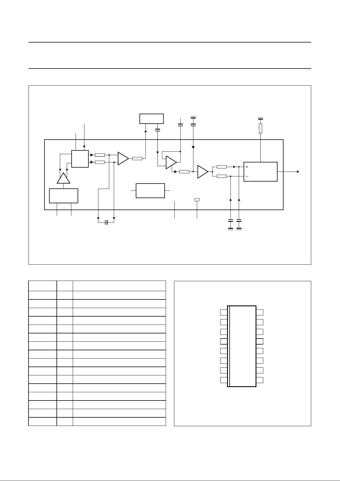
BLOCK DIAGRAM
handbook, full pagewidth
MHB679
OSCILLATOR
IF FILTER
161415
FA13LIN LFB CPC CPO
OSC OSE MON MOP CPACPB
BUFFER
×
MIXER
V
EE
V
EM MIXIN
RF_IN
BAND GAP
REFERENCE
V
CC
V
ref
LIMITER
IF AMPLIFIER
BUFFER
UAA3201T
COMPARATOR
R1
data
DATA
C14
C7
C19
C17
C12
C13
101112
9
768
V
CC
V
CC
345 12
Fig.1 Block diagram.
PINNING
SYMBOL PIN DESCRIPTION
MON 1 negative mixer output
MOP 2 positive mixer output
V
CC
3 positive supply voltage
OSC 4 oscillator collector
OSE 5 oscillator emitter
V
EE
6 negative supply voltage
CPB 7 comparator input B
CPA 8 comparator input A
DATA 9 data output
CPO 10 comparator offset adjustment
CPC 11 comparator input C
LFB 12 limiter feedback
LIN 13 limiter input
MIXIN 14 mixer input
V
EM
15 negative supply voltage for mixer
FA 16 IF amplifier output
UAA3201T
MED897
1
2
3
4
5
6
7
8
16
15
14
13
12
11
10
9
FA
V
EM
MIXIN
LIN
LFB
CPC
CPO
DATA
MON
MOP
V
CC
OSC
OSE
V
EE
CPB
CPA
Fig.2 Pin configuration.

2000 Apr 18 4
Philips Semiconductors Product specification
UHF/VHF remote control receiver UAA3201T
FUNCTIONAL DESCRIPTION
The RF signal is fed directly into the mixer stage where it
is mixed down to nominal 500 kHz IF by the integrated
oscillator controlledby anexternalSAWR (seeFig.1). The
IF signalisthenpassedtotheIF amplifierwhichincreases
the level. A 5th-order elliptic low-pass filter acts as main
IF filtering. The output voltage of that filter is demodulated
by a limiter that rectifies the incoming IF signal. The
demodulated signal passes two RC filter stages and is
thenlimited by a data comparator which makes it available
at the data output.
Mixer
The mixer is a single balanced emitter coupled pair with
internally set bias current. The optimum impedance is
320 Ω at 430 MHz. Capacitor C5 (see Fig.9) is used to
transform a 50 Ω generator impedance to the optimum
value.
Oscillator
The oscillator consists of a transistor in common base
configuration and a tank circuit including the SAWR.
Resistor R2 (see Fig.9) is used to control the bias current
through the transistor. Resistor R3 is required to reduce
unwanted responses of the tank circuit.
IF amplifier
The IF amplifier is a differential input, single-ended output
emitter coupled pair. It is used to decouple the first and the
second IF filter and to provide some additional gain in
order to reduce the influence of the noise of the limiter on
the total noise figure.
IF filters
The first IF filter is an RC filter formed by internal resistors
and an external capacitor C7 (see Fig.1).
The second IF filter is an external elliptic filter. The source
impedance is 1.4 kΩ and the load is high-impedance. The
bandwidth of the IF filter in the application and test circuit
(see Fig.9) is 800 kHz due to the centre frequency spread
of the SAWR. It may be reduced when SAWRs with less
tolerances are used or temperature range requirements
are lower. A smaller bandwidth of the filter will yield a
higher sensitivity of the receiver. As the RF signal is mixed
down to a low IF signal there is no image rejection
possible.
Limiter
The limiting amplifier consists of three DC coupled
amplifier stages with a total gain of 60 dB. A Received
Signal Strength Indicator (RSSI) signal is generated by
rectifying the IF signal. The limiter has a lower frequency
limitof 100 kHz which can be controlled by capacitors C12
and C19. The upper frequency limit is 3 MHz.
Comparator
The2 × IF component in the RSSI signalisremoved by the
first order low-pass capacitor C17. After passing a buffer
stage the signal is split into two paths, leading via
RC filters to the inputs of a voltage comparator. The time
constant of one path (C14) is compared to the bit duration.
Consequently the potential at the negative comparator
input represents the average magnitude of the RSSI
signal. The second path with a short time constant (C13)
allows the signal at the positive comparator input to follow
the RSSI signal instantaneously. This results in a variable
comparator threshold, depending on the strength of the
incoming signal. Hence the comparator output is switched
on, when the RSSI signal exceeds its average value, i.e.
when an ASK ‘on’ signal is received.
The low-pass filter capacitor C13 rejects the unwanted
2 × IF component and reduces the noise bandwidth of the
data filter.
The resistor R1 is used to set the current of an internal
source. This current is drawn from the positive comparator
input,therebyapplyinganoffsetanddriving the output into
the ‘off’ state during the absence of an input signal. This
offset can be increased by lowering the value of R1
yieldinga higher noise immunity at the expenseofreduced
sensitivity.
Band gap reference
The band gap reference controls the biasing of the whole
circuit. In this block currents are generated that are
constant over the temperature range and currents that are
proportional to the absolute temperature.
The current consumption of the receiver rises with
increasing temperature, because the blocks with the
highest current consumption are biased by currents that
are proportional to the absolute temperature.

2000 Apr 18 5
Philips Semiconductors Product specification
UHF/VHF remote control receiver UAA3201T
LIMITING VALUES
In accordance with the Absolute Maximum Rating System (IEC 60134).
Note
1. Human body model: equivalent to discharging a 100 pF capacitor through a 1.5 kΩ series resistor.
THERMAL CHARACTERISTICS
DC CHARACTERISTICS
V
CC
= 3.5 V; all voltages referenced to VEE; T
amb
= −40 to +85 °C; typical value for T
amb
=25°C; for test circuit
see Fig.9; SAWR disconnected; unless otherwise specified.
Note
1. I
DATA
is defined to be positive when the current flows into pin DATA.
SYMBOL PARAMETER CONDITIONS MIN. MAX. UNIT
V
CC
supply voltage −0.3 +8.0 V
T
amb
ambient temperature −40 +85 °C
T
stg
storage temperature −55 +125 °C
V
es
electrostatic handling voltage note 1
pins OSC and OSE −2000 +1500 V
pins LFB and MIXIN −1500 +2000 V
all other pins −2000 +2000 V
SYMBOL PARAMETER CONDITIONS VALUE UNIT
R
th(j-a)
thermal resistance from junction to ambient in free air 105 K/W
SYMBOL PARAMETER CONDITIONS MIN. TYP. MAX. UNIT
V
CC
supply voltage 3.5 − 6.0 V
I
CC
supply current R2 = 680 Ω−3.4 4.8 mA
V
OH(DATA)
HIGH-level output voltage at
pin DATA
I
DATA
= −10 µA; note 1 VCC− 0.5 − V
CC
V
V
OL(DATA)
LOW-level output voltage at
pin DATA
I
DATA
= +200 µA; note 1 0 − 0.6 V
2000 Apr 18 6
Philips Semiconductors Product specification
UHF/VHF remote control receiver UAA3201T
AC CHARACTERISTICS
VCC= 3.5 V; T
amb
=25°C; for test circuit see Fig.9; R1 disconnected; for AC test conditions see Section “AC test
conditions”; unless otherwise specified.
Notes
1. P
ref
is the maximum available power at the input of the test board. The Bit Error Rate (BER) is measured using the
test facility shown in Fig.8.
2. Valid only for the reference PCB (see Figs 10 and 11). Spurious radiation is strongly dependent on the PCB layout.
3. The supply voltage VCC is pulsed as explained in Fig.3.
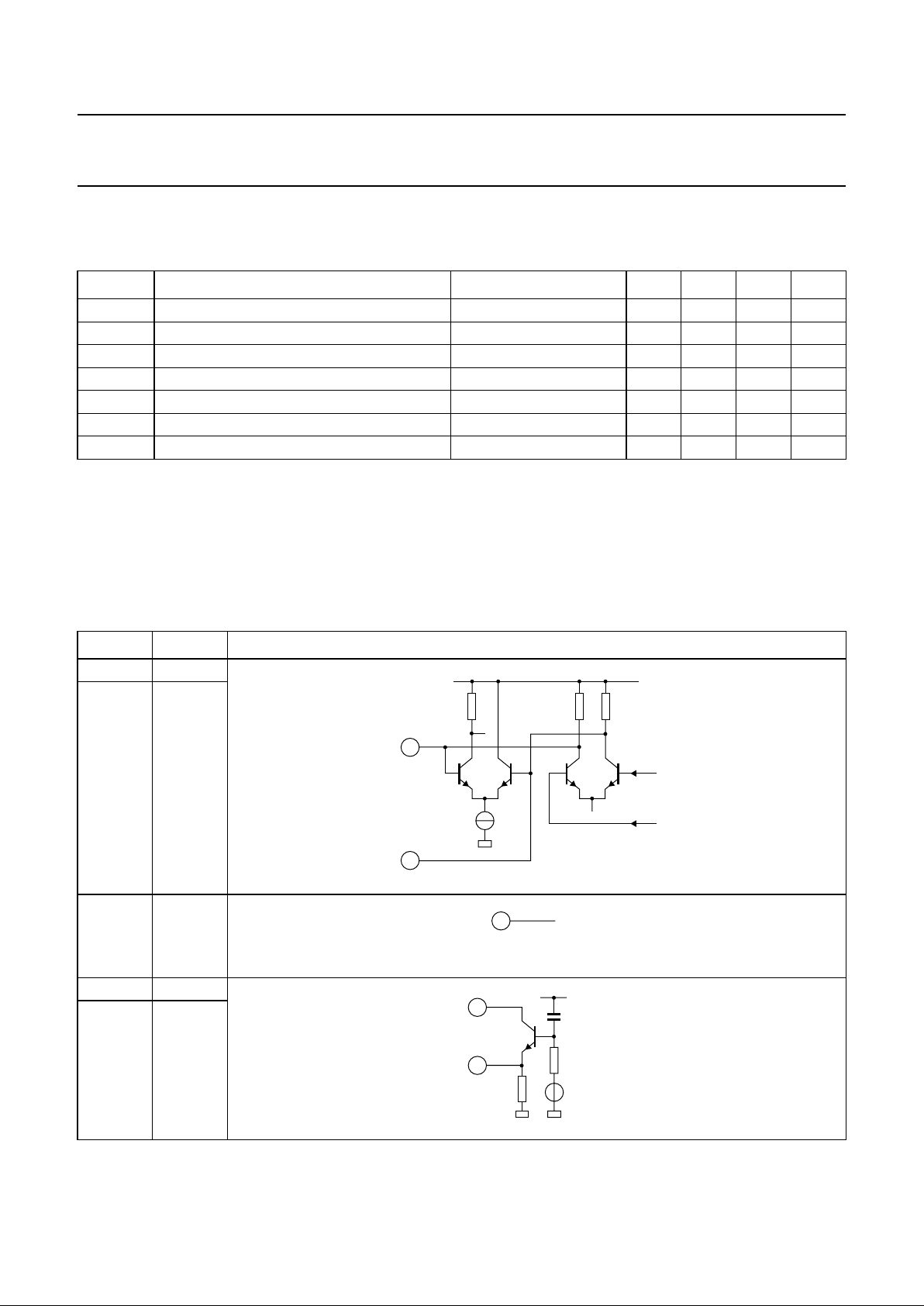
INTERNAL PIN CONFIGURATION
SYMBOL PARAMETER CONDITIONS MIN. TYP. MAX. UNIT
P
ref
input reference sensitivity BER ≤ 3 × 10⁻²; note 1 −−−105 dBm
P
i(max)
maximum input power BER ≤ 3 × 10
−2
−−−30 dBm
P
spur
spurious radiation note 2 −−−60 dBm
IP3
mix
interception point (mixer) −20 −17 − dBm
IP3
IF
interception point (mixer plus IFamplifier) −38 −35 − dBm
P
1dB
1 dB compression point (mixer) −38 −35 − dBm
t
on(RX)
receiver turn-on time note 3 −−10 ms
PIN SYMBOL EQUIVALENT CIRCUIT
1 MON
2 MOP
3V
CC
4 OSC
5 OSE
2
1
1.5
kΩ
1.5
kΩ
MHB680
V
P
from
oscillator
buffer
3
V
CC
MHB681
4
5
6 kΩ
1.2 V
V
P
MHB682
 Loading...