

Philips UAA2082U, UAA2082H Datasheet
INTEGRATED CIRCUITS
DATA SH EET
UAA2082
Advanced pager receiver
Product specification
Supersedes data of 1995 Nov 27
File under Integrated Circuits, IC03
1996 Jan 15
Philips Semiconductors Product specification
Advanced pager receiver UAA2082
FEATURES
• Wide frequency range: VHF, UHF and 900 MHz bands
• High sensitivity
• High dynamic range
• Electronically adjustable filters on chip
• Suitable for data rates up to 2400 bits/s
• Wide frequency offset and deviation range
• Fully POCSAG compatible FSK receiver
• Power on/off mode selectable by the chip enable input
• Low supply voltage; low power consumption
• 1-cell battery-low detection circuit
• High integration level
• Interfaces directly to the PCA5000A, PCF5001 and
PCD5003 POCSAG decoders.
APPLICATIONS
• Wide area paging
• On-site paging
• Telemetry
• RF security systems
• Low bit-rate wireless data links.
GENERAL DESCRIPTION
The UAA2082 is a high-performance low-power radio
receiver circuit primarily intended for VHF, UHF and
900 MHz pager receivers for wide area digital paging
systems, employing direct FM non-return-to-zero (NRZ)
frequency shift keying (FSK).
The receiver design is based on the direct conversion
principle where the input signal is mixed directly down to
the baseband by a local oscillator on the signal frequency.
Two complete signal paths with signals of 90° phase
difference are required to demodulate the signal.
All channel selectivity is provided by the built-in IF filters.
The circuit makes extensive use of on-chip capacitors to
minimize the number of external components.
The battery monitoring circuit has an external sense input
and a 1.1 V detection threshold for easy operation in a
single-cell supply concept.
The UAA2082 was designed to operate together with the
PCA5000A, PCF5001 or PCD5003 POCSAG decoders,
which contain a digital input filter for optimum call success
rate.
ORDERING INFORMATION
TYPE
NUMBER
UAA2082H LQFP32 plastic low profile quad flat package; 32 leads; body 7 × 7 × 1.4 mm SOT358-1
UAA2082U 28 pads naked die; see Fig.8
NAME DESCRIPTION VERSION
PACKAGE
1996 Jan 15 2
Philips Semiconductors Product specification
Advanced pager receiver UAA2082
QUICK REFERENCE DATA
SYMBOL PARAMETER CONDITIONS MIN. TYP. MAX. UNIT
V
P
I
P
I
P(off)
P
i(ref)
P
i(mix)
V
th
T
amb
supply voltage 1.9 2.05 3.5 V
supply current 2.3 2.7 3.2 mA
stand-by current −−3µA
RF input sensitivity BER ≤3⁄
data rate 1200 bits/s; T
f
i(RF)
f
i(RF)
f
i(RF)
mixer input sensitivity BER ≤3⁄
; ±4 kHz deviation;
100
=25°C
amb
= 173 MHz −−126.5 −123.5 dBm
= 470 MHz −−124.5 −121.5 dBm
= 930 MHz −−120.0 −114.0 dBm
; f
100
= 470 MHz;
i(RF)
−−115.0 −110.0 dBm
±4 kHz deviation;
detection threshold for battery
LOW indicator
data rate 1200 bits/s; T
T
=25°C 1.05 1.10 1.15 V
amb
= −10 to +70 °C 1.03 1.10 1.17 V
T
amb
amb
=25°C
operating ambient temperature −10 − +70 °C
1996 Jan 15 3
Philips Semiconductors Product specification
Advanced pager receiver UAA2082
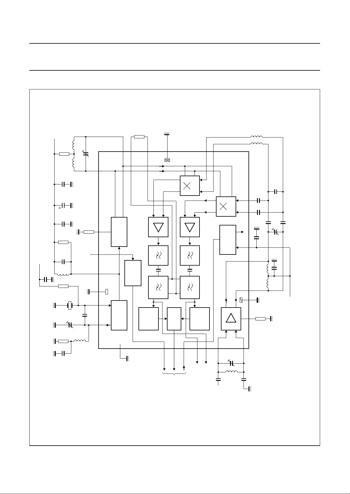
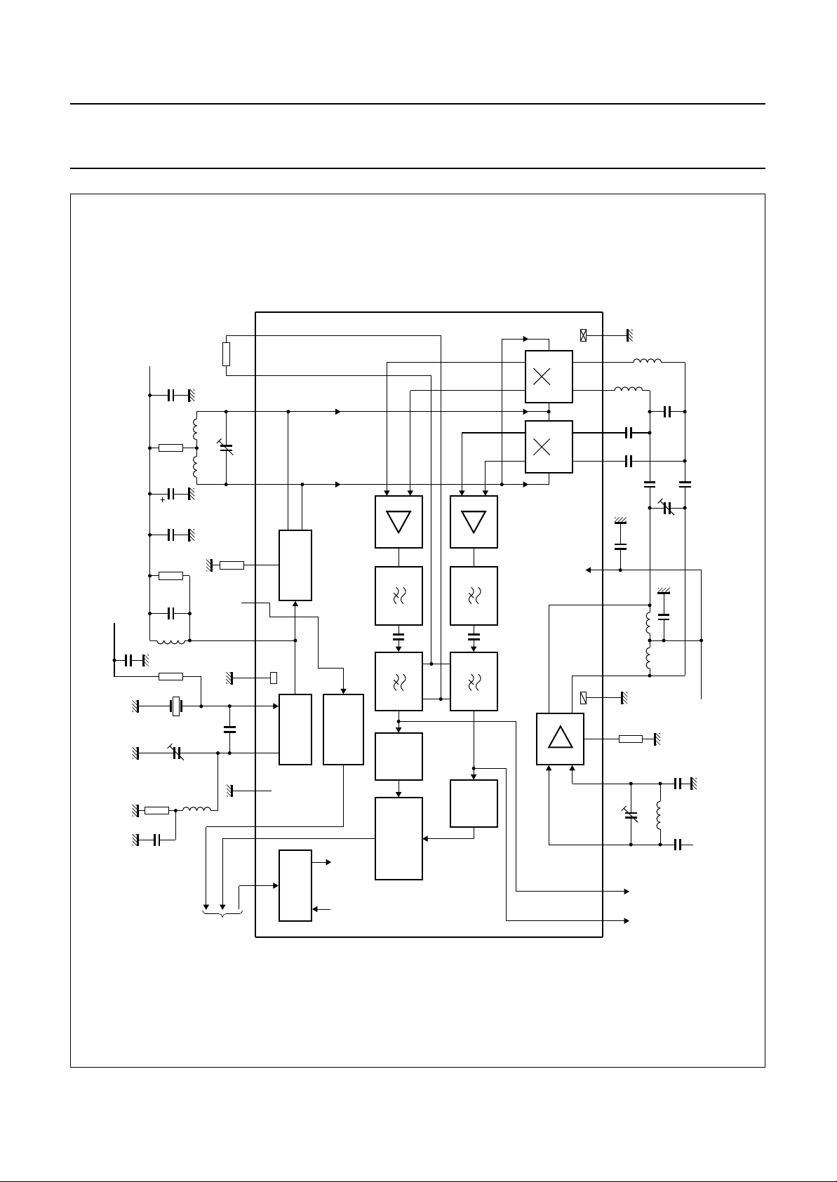
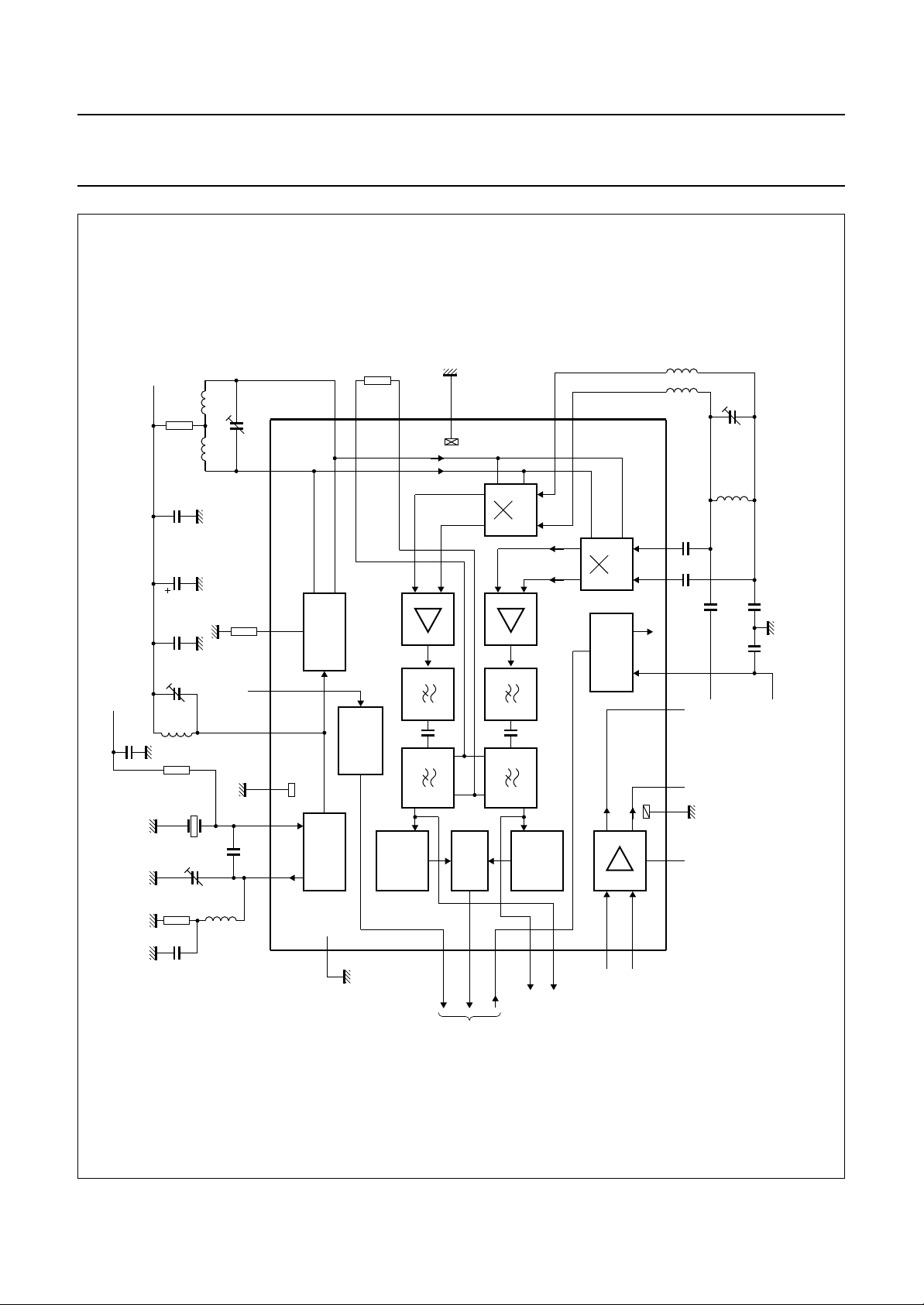
BLOCK DIAGRAMS (173 MHz)
L5
150
R2
47
P
V
kΩ
nH
bias(osc)
V
C20
1 nF
R3
C19
1.5 kΩ
C13
1 nF
10 µF
L6
33 nH
21
22
C12
5 to 20 pF
L7
33 nH
25
24
20
GND2
19
MIXER Q
C9
MLC222
8.2 pF
L4
nH
18
150
UAA2082H
C11
22 pF
= 172.941 MHz.
15 16
C14
1 nF
R4
2.2 kΩ
2627
low noise
LOW
BATTERY
INDICATOR
amplifier Q
ACTIVE
GYRATOR
Q
LIMITER
FILTER
FILTER
2
BLI
DEMO-
DULATOR
3
DO
ACTIVE
GYRATOR
4
RE
R7
100 Ω
C15
27 pF
L8
27
nH
R6
22
kΩ
XTAL
C16
R5
1.5
kΩ
C18
1 nF
13 to
L9
50 pF
560
SENSE
C17
nH
28
303132
GND3
15 pF
MULTIPLIER
FREQUENCY
CRYSTAL
OSCILLATOR
1TS
FILTER
FILTER
I
LIMITER
5
6
TPI
low noise
amplifier I
TPQ
MIXER I
BAND GAP
REFERENCE
RF pre-amplifier
7
C3
5 to
ref
V
P
V
13 14
12
11
10
8
20 pF
C10
L3
L2
GND1
330
22 pF
C5 1 nF
22 nH
22 nH
R1
Ω
C7
C6
8.2 pF
5 to
20 pF
C4 1 nF
C8
8.2 pF
P
V
i(RF)
handbook, full pagewidth
Fig.1 Block, test and application diagram drawn for LQFP32; f
1996 Jan 15 4
to
decoder
C1
8.2 pF
IF testpoints
i(RF)
V
L1
43
nH
C2
8.2 pF
Pins 9, 17, 23 and 29 are not connected.
Philips Semiconductors Product specification
Advanced pager receiver UAA2082
bias(osc)
V
C20
1 nF
V
P
C15
L8
R6
R5
C18
R3
C13
R7
1.5 kΩ
1 nF
C 19
1.5 kΩ
10 µF
C14
27
27
22
C16
1 nF
L6
L7
1 nF
100 Ω
pF
nH
kΩ
L9
XTAL
13 to
50 pF
560 nH
BLI
R2
33 nH
33 nH
C17
DO
47 kΩ
C12
R 4
2.2 kΩ
SENSE
15 pF
TS
RE
decoder
16 151718
5 to 20 pF
1920
21
222324
GND3
27 26 25
28
MULTIPLIER
FREQUENCY
CRYSTAL
BAND GAP
BATTERY
OSCILLATOR
ref
V
V
REFERENCE
Q
amplifier
low noise
UAA2082U
LOW
INDICATOR
P
FILTER
ACTIVE
FILTER
GYRATOR
Q
LIMITER
DEMODULATOR
FILTER
ACTIVE
FILTER
GYRATOR
I
LIMITER
I
amplifier
low noise
RF pre-amplifier
MIXER I MIXER Q
GND2
L5
150
nH
L4
150
nH
C9
10 11 12 13 14
89
7
6
54
12 3
10 pF 10 pF
L2
L3
R1
330
C3
TPI TPQ
C10 C11
C7
8.2 pF
C5 1 nF
22 nH
22 nH
GND1
Ω
5 to 20 pF
IF testpoints
MLC223
8.2 pF
C8
C6
5 to 20 pF
C4 1 nF
C2
8.2 pF
L1
43 nH
C1
8.2 pF
8.2 pF
P
V
i(RF)
V
= 172.941 MHz.
i(RF)
handbook, full pagewidth
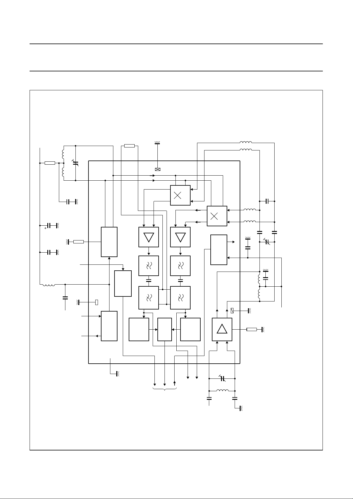
Fig.2 Block, test and application diagram drawn for naked die; f
1996 Jan 15 5
Philips Semiconductors Product specification
Advanced pager receiver UAA2082
Table 1 Tolerances of components shown in Figs 1 and 2 (notes 1 and 2)
COMPONENT
TOLERANCE
(%)
REMARK
Inductances
L1 ±5Q
L2, L3, L6, L7 ±20 Q
L4, L5 ±10 Q
L8 ±20 Q
L9 ±10 Q
= 100 at 173 MHz
min
= 50 at 173 MHz; TC = (+25 to +125) × 10−6/K
min
= 30 at 173 MHz; TC = (+25 to +125) × 10−6/K
min
= 30 at 173 MHz; TC = (+25 to +125) × 10−6/K
min
= 30 at 57 MHz; TC = (+25 to +125) × 10−6/K
min
Resistors
−6
R1 to R7 ±2 TC = +50 × 10
/K
Capacitors
C1, C2, C7, C8, C9, C15 ±5TC=(0±30) × 10−6/K; tan δ≤ 30 × 10−4at 1 MHz
−6
C3, C6, C12 − TC = (−750 ±300) × 10
C4, C5, C14, C18, C19, C20 ±10 TC = (0 ±30) × 10
C10, C11 ±5TC=(0±30) × 10
/K; tan δ≤50 × 10−4at 1 MHz
−6
/K; tan δ≤10 × 10−4at 1 MHz
−6
/K; tan δ≤21 × 10−4at 1 MHz
C13 ±20
−6
C16 − TC = (−1700 ±500) × 10
C17 ±5TC=(0±30) × 10
−6
/K; tan δ≤50 × 10−4at 1 MHz
/K; tan δ≤26 × 10−4at 1 MHz
Notes
1. Recommended crystal: f
= 57.647 MHz (crystal with 8 pF load), 3rd overtone, pullability >2.75 × 10⁻⁶/pF
XTAL
(change in frequency between series resonance and resonance with 8 pF series capacitor at 25 °C), dynamic
resistance R1 < 40 Ω, ∆f=±5×10⁻⁶ for T
= −10 to +55 °C with 25 °C reference, calibration plus aging tolerance:
amb
−5 × 10⁻⁶to +15 × 10−6.
2. This crystal recommendation is based on economic aspects and practical experience. Normally the spreads for R1,
pullability and calibration do not show their worst case limits simultaneously in one crystal. In such a rare event, the
tuning range will be reduced to an insufficient level.
1996 Jan 15 6
Philips Semiconductors Product specification
Advanced pager receiver UAA2082
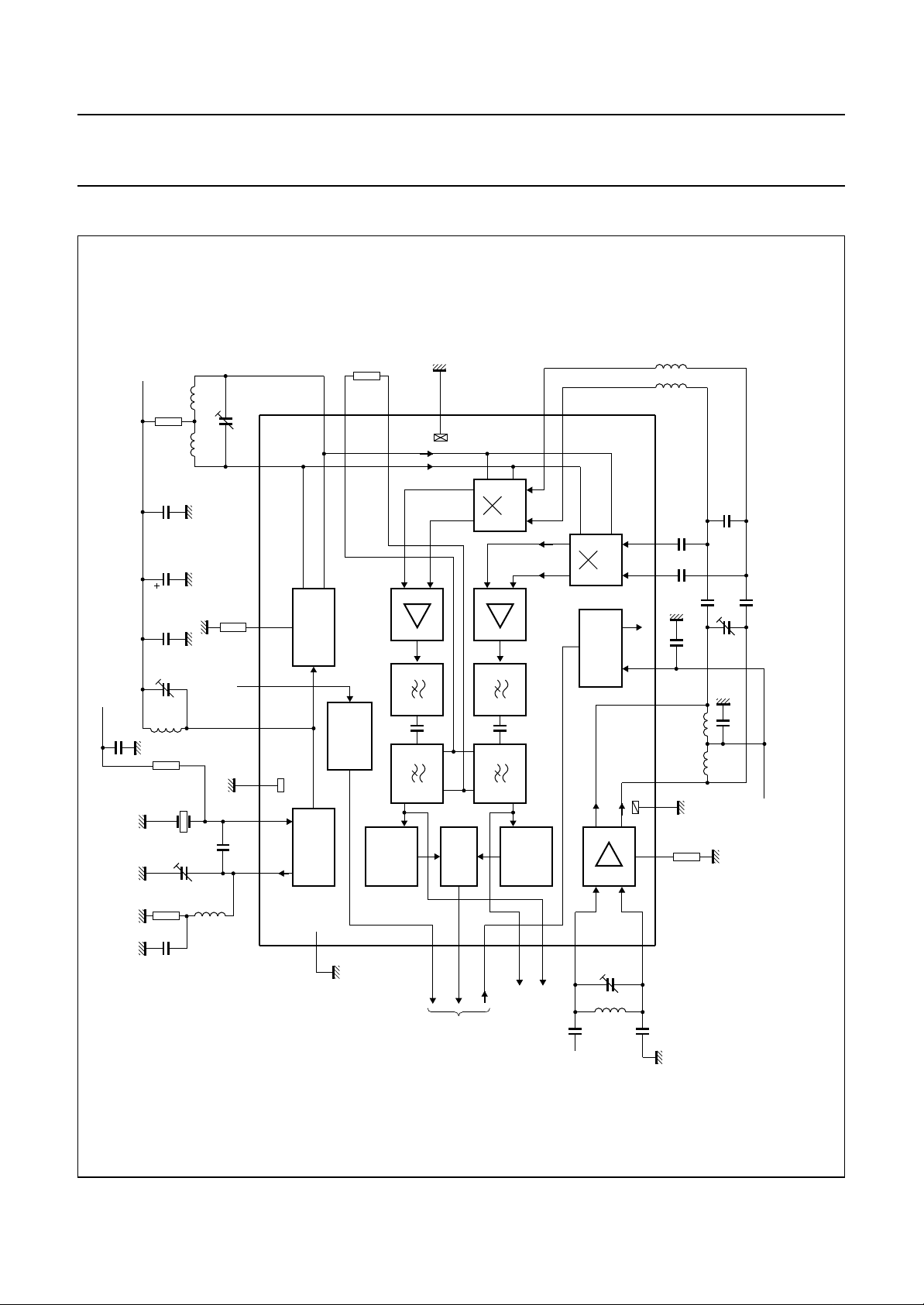
BLOCK AND TEST DIAGRAMS (470 MHz)
L5
40
R2
47
P
V
L6
820 Ω
1 nF
8 nH
C12
L7
8 nH
2.5 to 6 pF
25
24
R3
C19
kΩ
GND2
21
22
20
18
19
UAA2082H
MIXER Q
nH
C9
MLC224
2.7 pF
= 469.95 MHz.
L4
40
nH
C11
22 pF
bias(osc)
V
C20
1 nF
L8
R6
R5
C13
C14
100
22
1.5
C18
10 µF
1 nF
C15
1 nF
3 to
nH
kΩ
XTAL
C16
kΩ
10 pF
13 to
L9
50 pF
560
R4
1.2 kΩ
SENSE
C17
nH
GND3
15 pF
2627
28
303132
MULTIPLIER
FREQUENCY
LOW
BATTERY
CRYSTAL
OSCILLATOR
1TS
low noise
amplifier Q
ACTIVE
INDICATOR
GYRATOR
Q
LIMITER
FILTER
FILTER
2
BLI
DEMO-
DULATOR
3
4
DO
ACTIVE
GYRATOR
5
TPI
RE
low noise
amplifier I
FILTER
FILTER
I
LIMITER
6
TPQ
MIXER I
BAND GAP
REFERENCE
RF pre-amplifier
7
C3
2.5 to
ref
V
P
V
8
6 pF
15 16
C8
C7
C10
22 pF
C6
C5 1 nF
13 14
L3
8 nH
L2
GND1
330
8 nH
R1
Ω
12
11
10
2.7 pF
6 pF
2.5 to
C4 1 nF
2.7 pF
P
V
i(RF)
handbook, full pagewidth
Fig.3 Block, test and application diagram drawn for LQFP32; f
1996 Jan 15 7
to
decoder
C1
2.7 pF
IF testpoints
i(RF)
V
L1
nH
C2
12.5
2.7 pF
Pins 9, 17, 23 and 29 are not connected.
Philips Semiconductors Product specification
Advanced pager receiver UAA2082
bias(osc)
V
C20
1 nF
V
P
R5
C18
R3
C13
L8
R6
1.5 kΩ
1 nF
C 19
820 Ω
10 µF
C14
C15
100
22
1 nF
1 nF
3 to
nH
kΩ
C16
L6
L7
10 pF
XTAL
13 to
L9
R2
8 nH
8 nH
C17
50 pF
560 nH
DO
BLI
47 kΩ
C12
R 4
1.2 kΩ
SENSE
15 pF
TS
RE
decoder
16 151718
2.5 to 6 pF
1920
21
222324
GND3
27 26 25
28
MULTIPLIER
FREQUENCY
CRYSTAL
BAND GAP
BATTERY
OSCILLATOR
ref
V
V
REFERENCE
Q
amplifier
low noise
UAA2082U
LOW
INDICATOR
P
FILTER
ACTIVE
FILTER
GYRATOR
Q
LIMITER
DEMODULATOR
FILTER
ACTIVE
FILTER
GYRATOR
I
LIMITER
I
amplifier
low noise
RF pre-amplifier
MIXER I MIXER Q
GND2
L5
40
L4
40
nH
C9
10 11 12 13 14
89
7
6
54
12 3
22 pF 22 pF
L2
L3
R1
330
C3
TPI TPQ
C10 C11
C7
2.7 pF
C6
C5 1 nF
8 nH
8 nH
GND1
Ω
2.5 to 6 pF
IF testpoints
MLC225
nH
2.7 pF
C8
2.5 to 6 pF
C4 1 nF
C2
2.7 pF
L1
12.5 nH
C1
2.7 pF
2.7 pF
P
V
i(RF)
V
= 469.95 MHz.
i(RF)
handbook, full pagewidth
Fig.4 Block, test and application diagram drawn for naked die; f
1996 Jan 15 8
Philips Semiconductors Product specification
Advanced pager receiver UAA2082
L5
40
R2
47
P
V
L6
820 Ω
1 nF
8 nH
C12
L7
8 nH
2.5 to 6 pF
24
25
R3
C19
kΩ
GND2
21
22
20
18
19
UAA2082H
MIXER Q
nH
L4
40
nH
C11
22 pF
MLC226
C23
2.5 to 6 pF
L10
12.5 nH
bias(osc)
V
C20
1 nF
L8
R6
R5
C13
C14
100
22
1.5
C18
10 µF
1 nF
C15
1 nF
3 to
nH
kΩ
XTAL
C16
kΩ
10 pF
13 to
50 pF
L9
560
R4
1.2 kΩ
SENSE
C17
nH
GND3
15 pF
2627
28
303132
MULTIPLIER
FREQUENCY
LOW
BATTERY
CRYSTAL
OSCILLATOR
1TS
low noise
amplifier Q
ACTIVE
INDICATOR
GYRATOR
Q
LIMITER
FILTER
FILTER
2
BLI
DEMO-
DULATOR
3
DO
ACTIVE
GYRATOR
5
4
TPI
RE
low noise
FILTER
FILTER
I
LIMITER
6
TPQ
amplifier I
RF pre-amplifier
7
MIXER I
V
BAND GAP
REFERENCE
V
8
ref
P
15 16
= 469.95 MHz.
5.6 pF
i(RF)
handbook, full pagewidth
P
C21
C5
C22
5.6 pF
1 nF
V
C10
22 pF
13 14
12
1110
GND1
i(RF)
V
Fig.5 Mixer input sensitivity test circuit; f
1996 Jan 15 9
to
IF testpoints
decoder
Philips Semiconductors Product specification
Advanced pager receiver UAA2082
Table 2 Tolerances of components shown in Figs 3, 4 and 5 (notes 1 and 2)
COMPONENT
TOLERANCE
(%)
REMARK
Inductances
L1, L10 ±5Q
L2, L3, L6, L7 ±20 Q
L4, L5 ±10 Q
L8 ±10 Q
L9 ±10 Q
= 145 at 470 MHz
min
= 50 at 470 MHz; TC = (+25 to +125) × 10−6/K
min
= 40 at 470 MHz; TC = (+25 to +125) × 10−6/K
min
= 30 at 156 MHz; TC = (+25 to +125) × 10−6/K
min
= 40 at 78 MHz; TC = (+25 to +125) × 10−6/K
min
Resistors
−6
R1 to R6 ±2 TC = +50 × 10
/K
Capacitors
C1, C2, C7, C8, C9 ±5TC=(0±30) × 10−6/K; tan δ≤30 × 10−4 at 1 MHz
−6
C3, C6, C12, C23 − TC = (−750 ±300) × 10
C4, C5, C14, C18 to C22 ±10 TC = (0 ±30) × 10
C10, C11 ±5TC=(0±30) × 10
/K; tan δ≤50 × 10−4at 1 MHz
−6
/K; tan δ≤10 × 10−4 at 1 MHz
−6
/K; tan δ≤21 × 10−4 at 1 MHz
C13 ±20
−6
C16 − TC = (−1700 ±500) × 10
C17 ±5TC=(0±30) × 10
−6
/K; tan δ≤50 × 10−4at 1 MHz
/K; tan δ≤26 × 10−4at 1 MHz
Notes
1. Recommended crystal: f
= 78.325 MHz (crystal with 8 pF load), 3rd overtone, pullability >2.75 × 10⁻⁶/pF
XTAL
(change in frequency between series resonance and resonance with 8 pF capacitor at 25 °C), dynamic resistance
R1 < 30 Ω, ∆f=±5×10⁻⁶ for T
= −10 to +55 °C with 25 °C reference, calibration plus aging tolerance:
amb
−5 × 10⁻⁶to +15 × 10−6.
2. This crystal recommendation is based on economic aspects and practical experience. Normally the spreads for R1,
pullability and calibration do not show their worst case limits simultaneously in one crystal. In such a rare event, the
tuning range will be reduced to an insufficient level.
1996 Jan 15 10
Philips Semiconductors Product specification
Advanced pager receiver UAA2082
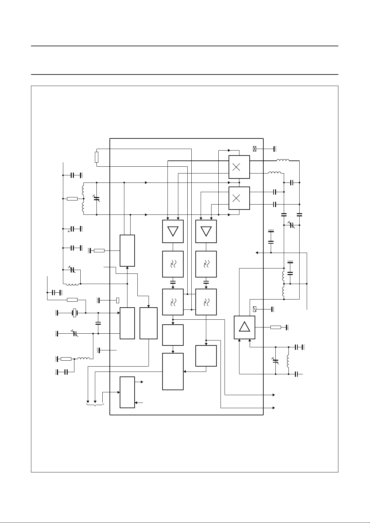
BLOCK AND TEST DIAGRAM (930 MHz)
L5
12.5
R2
47
P
V
L6
R3
330 Ω
3 nH
C12
3 nH
1.7 to 3 pF
25
L7
24
22
kΩ
GND2
21
20
18
19
nH
L4
nH
12.5
MLC227
C13
C14
L8
4.7 µF
150
pF
33 nH
C15
C19
150 pF
3.3 pF
i(OSC)
V
R4
390 Ω
SENSE
2627
28
303132
GND3
MULTIPLIER
FREQUENCY
LOW
BATTERY
CRYSTAL
OSCILLATOR
1TS
low noise
amplifier Q
ACTIVE
INDICATOR
GYRATOR
Q
LIMITER
FILTER
FILTER
2
DEMO-
DULATOR
3
4
MIXER Q
FILTER
ACTIVE
FILTER
GYRATOR
LIMITER
5
low noise
amplifier I
I
6
MIXER I
BAND GAP
REFERENCE
RF pre-amplifier
7
UAA2082H
L11
15 16
L10
ref
V
C5
P
V
13 14
L3
L2
12
11
GND1
10
120
8
5 nH
5 nH
150 pF
3.5 nH
3.5 nH
R1
Ω
C7
C6
C9
1.7 to
1.2 pF
1.5 pF
C8
1.5 pF
3 pF
C4 150 pF
P
V
= 930.50 MHz.
i(RF)
handbook, full pagewidth
Fig.6 Test circuit; f
RE
DO
BLI
to
decoder
1996 Jan 15 11
TPI
TPQ
IF testpoints
C1
1.2 pF
i(RF)
V
C3
3 pF
1.7 to
5
L1
nH
C2
1.0 pF
Pins 9, 17, 23 and 29 are not connected.
Philips Semiconductors Product specification
Advanced pager receiver UAA2082
Table 3 Tolerances of components shown in Fig.6 (note 1)
COMPONENT
TOLERANCE
(%)
REMARK
Inductances
L1 ±10 Q
= 150 at 930 MHz
typ
L2, L3, L6, L7 − microstrip inductor
L4, L5 ±5Q
L8 ±10 Q
L10, L11 ±10 Q
= 100 at 930 MHz
typ
= 65 at 310 MHz
typ
= 150 at 930 MHz
typ
Resistors
−6
R1 to R4 ±2TC=(0±200) × 10
/K
Capacitors
C1, C2, C7, C8, C9, C15 ±5TC=(0±30) × 10−6/K; tan δ≤30 × 10−4at 1 MHz
−6
C3, C6, C12 − TC = (0 ±200) × 10
C4, C5, C14, C19 ±10 TC = (0 ±30) × 10
/K; tan δ≤30 × 10−4at 1 MHz
−6
/K; tan δ≤10 × 10−4at 1 MHz
C13 ±20
Note
1. The external oscillator signal V
has a frequency of f
i(OSC)
= 310.1667 MHz.
OSC
1996 Jan 15 12
 Loading...