

Philips UAA2077TS Datasheet

INTEGRATED CIRCUITS
DATA SH EET
UAA2077TS
2 GHz image rejecting front-end
Preliminary specification
Supersedes data of 2000 Mar 09
File under Integrated Circuits, IC17
2000 Apr 17
Philips Semiconductors Preliminary specification
2 GHz image rejecting front-end UAA2077TS
FEATURES
• Low noise, wide dynamic range amplifier
• Very low noise figure
• Dual balanced mixers for over 30 dB on-chip image
rejection
• Quadrature 200 MHz IF recombiner
• On-chip quadrature network
• Independent SX, RX, power-down control modes and
fast power-up switching
• Very small outline packaging
• No image filter required, resulting in a very small
application.
APPLICATIONS
• GSM dual band solution with UAA3522HL
• High frequency front-end for DCS1800/PCS1900
portable hand-held equipment
• Compact mobile digital communication equipment
• Time Division Multiple Access (TDMA) receivers e.g.
RF Local Area Networks (RF LANs).
GENERAL DESCRIPTION
The UAA2077TS contains a 2 GHz front-end receiver
intended to beusedin mobile telephones. Designed in an
advanced BiCMOS process itcombines high performance
with a low power consumption and high integration, thus
reducing external component costs and overall front-end
size.
The main advantage of the UAA2077TS is its ability to
provide an image rejection over 30 dB. Therefore, an
additional image filter between the Low Noise Amplifier
(LNA) and the mixer is not required.
Image rejection is achieved internally by two RF mixers in
quadrature operation andtwo all-pass filters in the I and Q
IF channels that shift thephase of signals by 45° and 135°
respectively. These two phase shifted IF signals are
combined and buffered to the front-end IF output signal.
Aninput signal witha frequency above theLocal Oscillator
(LO)frequency results in anIF signal, while an input signal
with a frequency below the LO frequency is rejected.
The receive section consists of an LNA that drives a
quadrature mixer pair. The IF amplifier consists of an
on-chip45° and 135°phaseshiftingnetwork and an image
reject IF recombiner. The IF driver has differential
open-collector outputs.
The LO part consists of an internal all-pass phase shifting
filter to providethe quadrature LO signals for themixers of
the receive section. The all-pass filter output signals are
buffered before being fed to the mixers. All RF inputs and
IF outputs are balanced.
Pins RXON and SXON allow control of the different active
modes and power-down. The SX mode and the RX mode
are independent active states of the LO section and the
receive section respectively. When the logic level on
pin SXONis HIGH, all internalbuffers in the LO pathof the
circuit are turned on, thus minimizing LO pulling during the
independent powering up of the receive section. Special
care has been taken by design for fast switching from
power-down to any of the different active modes.
QUICK REFERENCE DATA
SYMBOL PARAMETER CONDITIONS MIN. TYP. MAX. UNIT
V
CC
I
CC(pd)
I
CC(SRX)
T
amb
supply voltage 2.7 2.8 3.3 V
power-down supply current −−50 µA
supply current in SRX mode − 25 28 mA
ambient temperature −30 +25 +70 °C
ORDERING INFORMATION
TYPE
NUMBER
NAME DESCRIPTION VERSION
PACKAGE
UAA2077TS/D SSOP16 plastic shrink small outline package; 16 leads; body width 4.4 mm SOT369-1
2000 Apr 17 2
Philips Semiconductors Preliminary specification
2 GHz image rejecting front-end UAA2077TS
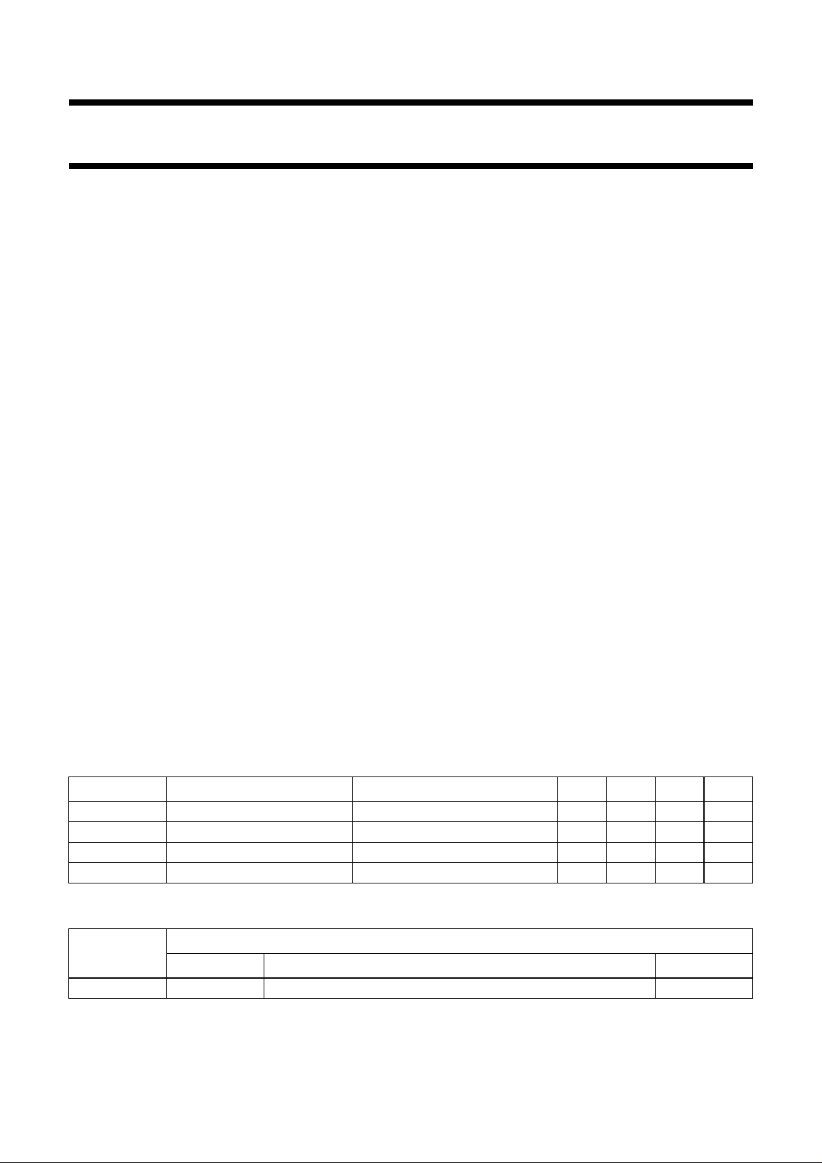
BLOCK DIAGRAM
V
handbook, full pagewidth
CCLNA
LNAGND
GND
n.c.
RXON
1 6
RFINA
RFINB
3
LNA
4
×
×
V
CCLO
LOGND
PINNING
SYMBOL PIN DESCRIPTION
V
CCLNA
1 supply voltage for receive section
(LNA and IF parts)
n.c. 2 not connected
RFINA 3 RF input A (balanced)
RFINB 4 RF input B (balanced)
n.c. 5 not connected
LNAGND 6 ground for receive section (LNA and
IF parts)
SXON 7 SX mode enable input (see Table 1)
n.c. 8 not connected
GND 9 ground
RXON 10 RX mode enable input (see Table 1)
LOINB 11 LO input B (balanced)
LOINA 12 LO input A (balanced)
V
CCLO
13 supply voltage for LO section
LOGND 14 ground for LO section
IFA 15 IF output A (balanced)
IFB 16 IF output B (balanced)
13
135
14
7
SXON
°
QUADRATURE
PHASE
SHIFTER
LOINB LOINA
Fig.1 Block diagram.
2, 5, 8
9
45
10
45
°
COMBINER
°
135
RECEIVE SECTION
LOCAL OSCILLATOR SECTION
°
15
IFA
IF
16
IFB
UAA2077TS
11
12
FCA012
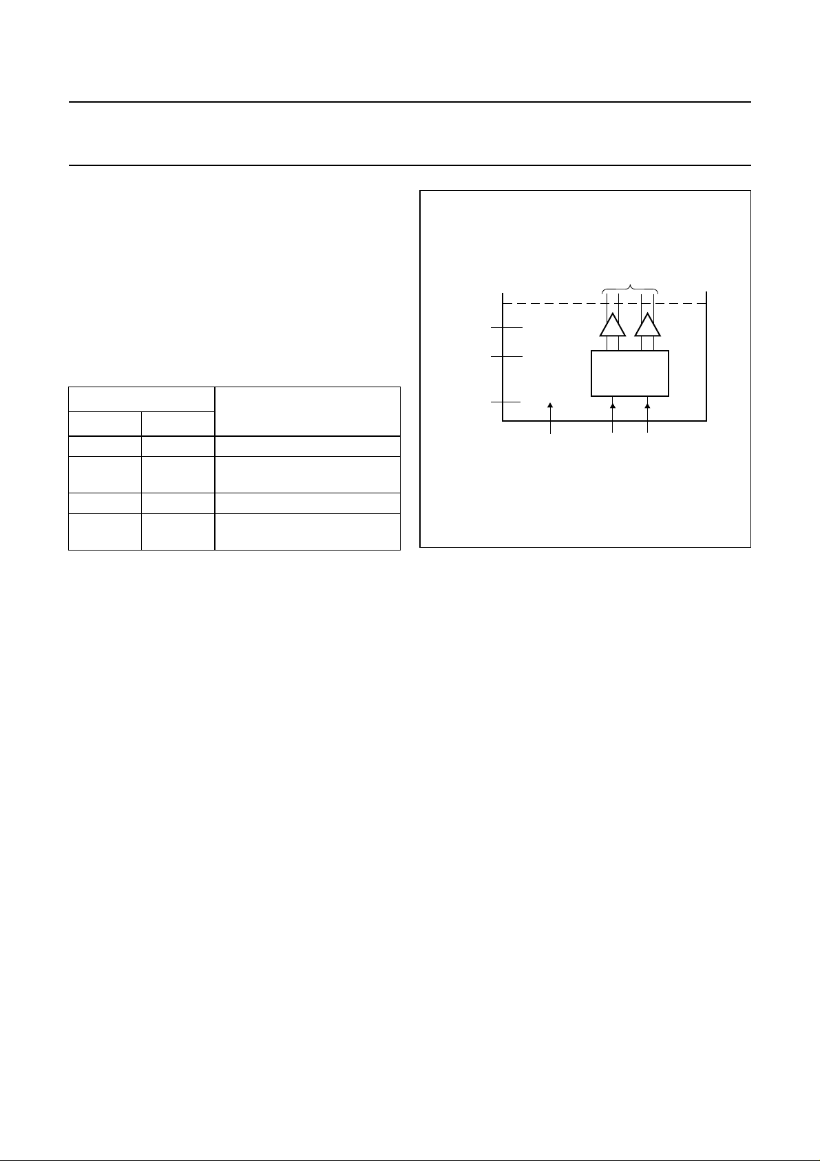
handbook, halfpage
V
CCLNA
n.c.
RFINA
RFINB
n.c.
LNAGND
SXON
n.c.
1
2
3
4
UAA2077TS
5
6
7
8
FCA011
16
15
14
13
12
11
10
9
IFB
IFA
LOGND
V
CCLO
LOINA
LOINB
RXON
GND
Fig.2 Pin configuration.
2000 Apr 17 3
Philips Semiconductors Preliminary specification
2 GHz image rejecting front-end UAA2077TS
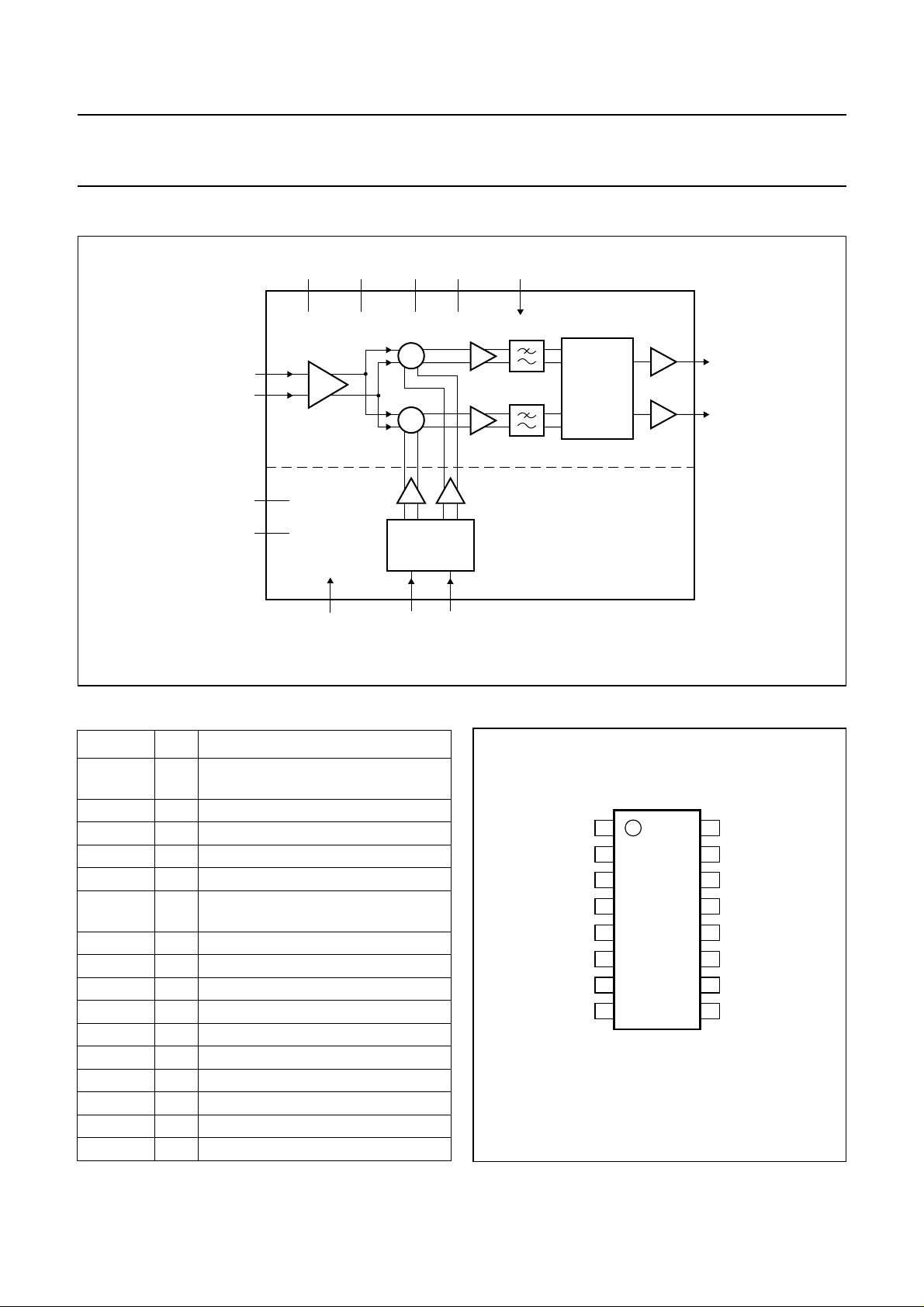
FUNCTIONAL DESCRIPTION
Receive section
The circuit contains a low-noise amplifier followed by two
high dynamic range mixers (see Fig.3). The mixers are of
the Gilbert cell type, the architecture of which is fully
differential.
The LO signal is phase shifted into 45° and 135° signals,
mixed with the RF input signal to provide the
I and Q channel signals. The I and Q channel signals are
buffered, phase shifted by 45° and 135° respectively,
amplified and internally combined, thus obtaining image
rejection.
Balanced signal interfaces are used for minimizing
crosstalk from package parasitics.
handbook, full pagewidth
RFINA
RFINB
CCLNA
3
4
1
LNA
LNAGND
6
GND
9
×
V
×
The IF output is of a differential open collector type.
A typical application consists of pull-up resistors of 680 Ω
at each IF output and a differential load resistance of 1 kΩ
for the IF filter, due to its impedance or its matching
network.
The power gain refers to the resulting power into the 1 kΩ
load. The path for the DC current from VCC into the open
collector outputs should be realized by the inductors.
The output signal is limited to VCC+3VBE.
Fast switching between power-down and the RX mode is
controlled by the mode control pin RXON.
n.c.
2, 5, 8
RXON
10
45°
135°
UAA2077TS
IF
COMBINER
15
IFA
16
IFB
to LO section
Fig.3 Receive section.
2000 Apr 17 4
FCA013
Philips Semiconductors Preliminary specification
2 GHz image rejecting front-end UAA2077TS
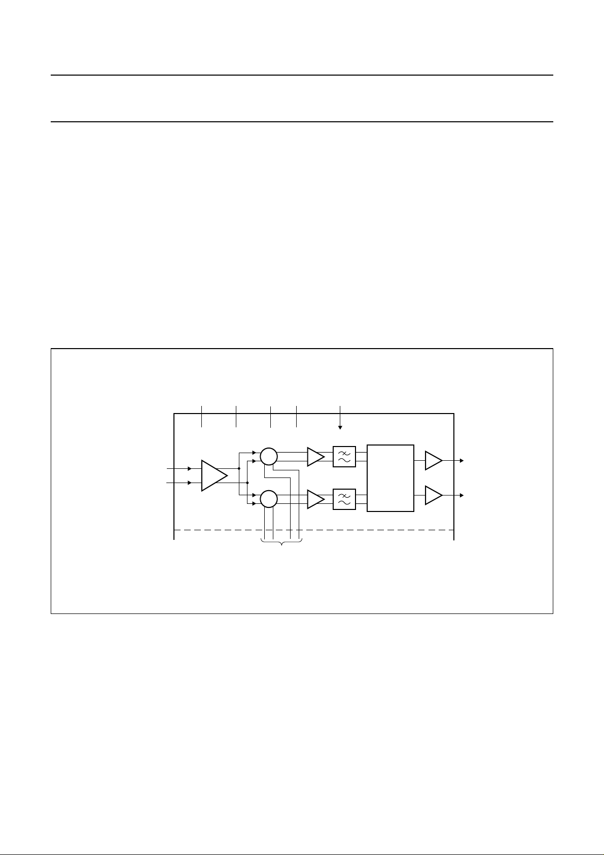
Local oscillator section
The LO input directly drives the two internal all-pass
networks to provide the quadrature signals for the mixers
(see Fig.4).
The SX mode (see Table 1) is used to activate the
LO section, thus minimizingpulling of the external Voltage
Controlled Oscillator (VCO) when enabling the receive
section. The SX mode is active when the logic level on pin
SXON is HIGH.
Table 1 Operating modes
LOGIC LEVEL
MODE
PIN RXON PIN SXON
LOW LOW Power-down mode
HIGH LOW RX mode; receive section
active
LOW HIGH SX mode; LO section active
HIGH HIGH SRX mode; both sections
active
handbook, halfpage
V
CCLO
LOGND
GND
13
14
UAA2077TS
9
7
SXON
Fig.4 LO section.
to receive section
135
°
QUADRATURE
PHASE
SHIFTER
11
LOINB
12
LOINA
45°
FCA014
2000 Apr 17 5
 Loading...