


INTEGRATED CIRCUITS
DATA SH EET
UAA2077BM
2 GHz image rejecting front-end
Product specification
Supersedes data of July 1995
File under Integrated Circuits, IC03
1995 Dec 13

Philips Semiconductors Product specification
2 GHz image rejecting front-end UAA2077BM
FEATURES
• Low-noise, wide dynamic range amplifier
• Very low noise figure
• Dual balanced mixer for over 25 dB on-chip image
rejection
• IF I/Q combiner at 188 MHz
• On-chip quadrature network
• Down-conversion mixer for closed-loop transmitters
• Independent TX/RX fast ON/OFF power-down modes
• Very small outline packaging
• Very small application (no image filter).
APPLICATIONS
• 1800 MHz front-end for DCS1800 hand-portable
equipment
• Compact digital mobile communication equipment
• TDMA receivers e.g. PCS and RF-LANS.
GENERAL DESCRIPTION
UAA2077BM contains both a receiver front-end and a high
frequency transmit mixer intended to be used in mobile
telephones. Designed in an advanced BiCMOS process it
combines high performance with low power consumption
and a high degree of integration, thus reducing external
component costs and total front-end size.
The main advantage of the UAA2077BM is its ability to
provide over 25 dB of image rejection. Consequently, the
image filter between the LNA and the mixer is suppressed.
Image rejection is achieved in the internal architecture by
two RF mixers in quadrature and two all-pass filters in
I and Q IF channels that phase shift the IF by 45° and 135°
respectively. The two phase shifted IFs are recombined
and buffered to furnish the IF output signal.
For instance, signals presented at the RF input at the
LO + IF frequency are rejected through this signal
processing while signals at the LO − IF frequency can form
the IF signal. An internal switch enables the upper or lower
image frequency to be rejected.
The receiver section consists of a low-noise amplifier that
drives a quadrature mixer pair. The IF amplifier has
on-chip 45° and 135° phase shifting and a combining
network for image rejection. The IF driver has differential
open-collector type outputs.
The LO part consists of an internal all-pass type phase
shifter to provide quadrature LO signals to the receive
mixers. The centre frequency of the phase shifter is
adjustable for maximum image rejection in a given band.
The all-pass filters outputs are buffered before being fed to
the receive mixers.
The transmit section consists of a low-noise amplifier and
a down-conversion mixer. In the transmit mode an internal
LO buffer is used to drive the transmit IF down-conversion
mixer.
All RF and IF inputs or outputs are balanced.
Pins RXON, TXON and SXON enable a selection to be
made of whether to reject the upper or lower image
frequency and control of the different power-down modes.
Special care has been taken for fast power-up switching.
QUICK REFERENCE DATA
SYMBOL PARAMETER MIN. TYP. MAX. UNIT
V
CC
I
CC(RX)
I
CC(TX)
I
CC(PD)
T
amb
supply voltage 3.6 4.0 5.3 V
receive supply current 21.5 26.5 33.5 mA
transmit supply current 10.5 13.5 18 mA
supply current in power-down −−50 µA
operating ambient temperature −30 +25 +85 °C
ORDERING INFORMATION
TYPE
NUMBER
NAME DESCRIPTION VERSION
PACKAGE
UAA2077BM SSOP20 plastic shrink small outline package; 20 leads; body width 4.4 mm SOT266-1
1995 Dec 13 2
Philips Semiconductors Product specification
2 GHz image rejecting front-end UAA2077BM
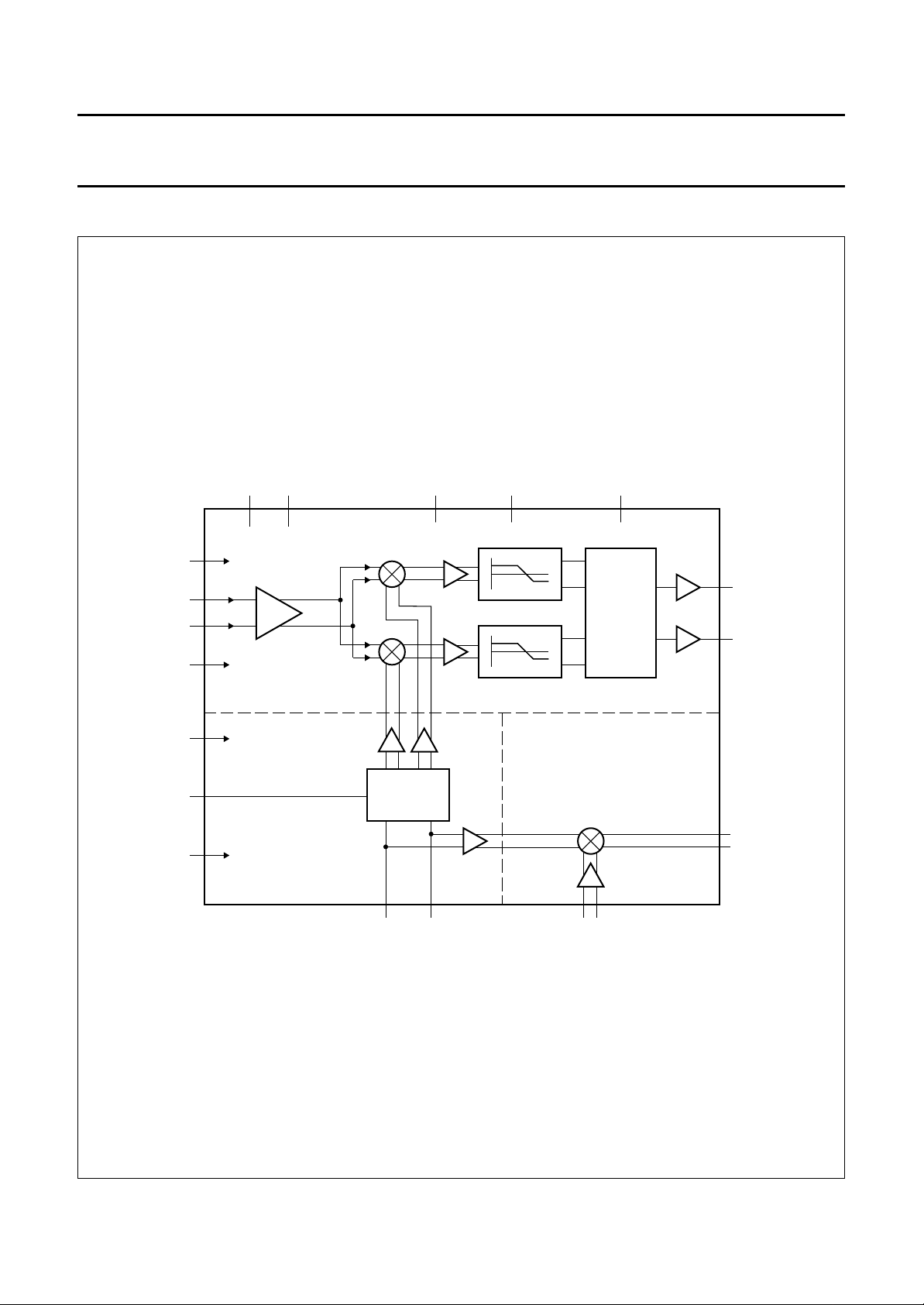
BLOCK DIAGRAM
handbook, full pagewidth
V
CCLNA
RFINA
RFINB
LNAGND
V
CCLO
V
QUADLO
LOGND
n.c. n.c. SXON
4 7
3
5
6
8
UAA2077BM
LNA
low-noise
amplifier
MIXER
TXON
RXON
11
12
+45
+135
o
o
RECEIVE SECTION
15
10
16
QUADRATURE
PHASE
SHIFTER
TRANSMIT SECTION
LOCAL OSCILLATOR
SECTION
LOINA
COMBINER
MIXER
11314 2
TXINATXINBLOINB
9
17
IFA
IF
18
IFB
19
TXOA
TXOB
20
MGD154
Fig.1 Block diagram.
1995 Dec 13 3
Philips Semiconductors Product specification
2 GHz image rejecting front-end UAA2077BM
PINNING
SYMBOL PIN DESCRIPTION
TXINA 1 transmit mixer input A (balanced)
TXINB 2 transmit mixer input B (balanced)
V
CCLNA
n.c. 4 not connected
RFINA 5 RF input A (balanced)
RFINB 6 RF input B (balanced)
n.c. 7 not connected
LNAGND 8 ground for LNA, IF parts and TX
SXON 9 SX mode enable (see Table 1)
V
QUADLO
TXON 11 TX mode enable (see Table 1)
RXON 12 RX mode enable (see Table 1)
LOINB 13 LO input B (balanced)
LOINA 14 LO input A (balanced)
V
CCLO
LOGND 16 ground for LO parts
IFA 17 IF output A (balanced)
IFB 18 IF output B (balanced)
TXOA 19 transmit mixer IF output A
TXOB 20 transmit mixer IF output B
3 supply voltage for LNA, IF parts
and TX mixer
mixer
10 input voltage for LO quadrature
trimming
15 supply voltage for LO parts
(balanced)
(balanced)
handbook, halfpage
LNAGND
V
QUADLO
1
TXINA
2
TXINB
n.c.
RFINA
RFINB
n.c.
SXON
3
4
5
UAA2077BM
6
7
8
9
10
V
CCLNA
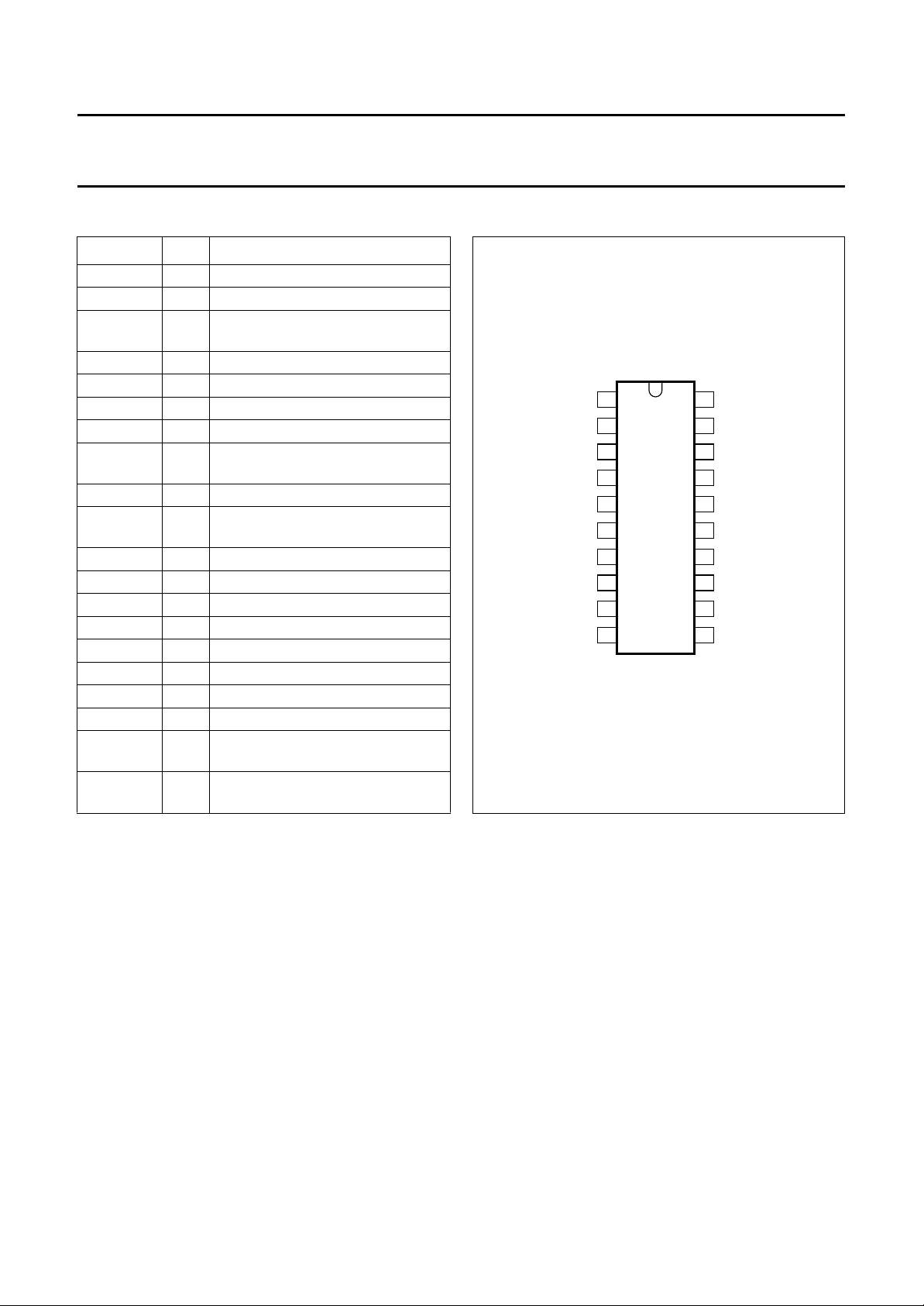
Fig.2 Pin configuration.
MGD155
20
19
18
17
16
15
14
13
12
11
TXOB
TXOA
IFB
IFA
LOGND
V
CCLO
LOINA
LOINB
RXON
TXON
1995 Dec 13 4
Philips Semiconductors Product specification
2 GHz image rejecting front-end UAA2077BM
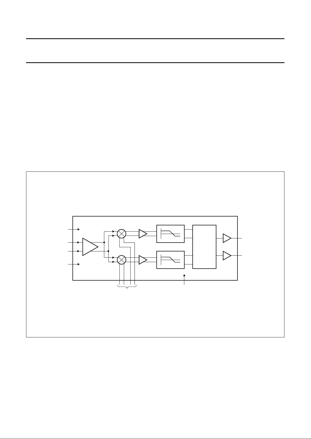
FUNCTIONAL DESCRIPTION
Receive section
The circuit contains a low-noise amplifier followed by two
high dynamic range mixers. These mixers are of the
Gilbert-cell type, the whole internal architecture is fully
differential.
The local oscillator, shifted in phase to 45° and 135°,
mixes the amplified RF to create I and Q channels.
The two I and Q channels are buffered, phase shifted by
45° and 135° respectively, amplified and recombined
internally to realize the image rejection.
Balanced signal interfaces are used for minimizing
crosstalk due to package parasitics.
handbook, full pagewidth
V
CCLNA
MIXER
IF
amplifier
The IF output is differential and of the open-collector type.
Typical application will load the output with a differential
1kΩ load; for example, a 1 kΩ resistor load at each IF
output, plus a differential 2 kΩ load consisting of the input
impedance of the IF filter or the input impedance of the
matching network for the IF filter. The power gain refers to
the available power on this 2 kΩ load. The path to V
CC
for
the DC current should be achieved via tuning inductors.
The output voltage is limited to VCC+3Vbe or 3 diode
forward voltage drops.
Fast switching, ON/OFF, of the receive section is
controlled by the hardware input RXON.
o
+45
RFINA
RFINB
LNAGND
LNA
MIXER
IF
amplifier
LOIN
+135
o
RXON
Fig.3 Block diagram, receive section.
IFA
IF
COMBINER
IFB
MGD157
1995 Dec 13 5
 Loading...