

Philips UAA2073AM Datasheet

INTEGRATED CIRCUITS
DATA SH EET
UAA2073AM
Image rejecting front-end
for GSM applications
Product specification
Supersedes data of 1996 Oct 23
File under Integrated Circuits, IC17
1997 Jan 27

Philips Semiconductors Product specification
Image rejecting front-end
for GSM applications
FEATURES
• Low-noise, wide dynamic range amplifier
• Very low noise figure
• Dual balanced mixer for at least 30 dB on-chip image
rejection
• IF I/Q combination network for 175 MHz
• Down-conversion mixer for closed-loop transmitters
• Independent TX/RX fast on/off power-down modes
• Very small outline packaging
• Very small application (no image filter).
APPLICATIONS
• 900 MHz front-end for GSM hand-portable equipment
• Compact digital mobile communication equipment
• TDMA receivers.
GENERAL DESCRIPTION
UAA2073AM contains both a receiver front-end and a high
frequency transmit mixer intended for GSM
(Global System for Mobile communications) cellular
telephones. Designed in an advanced BiCMOS process it
combines high performance with low power consumption
and a high degree of integration, thus reducing external
component costs and total front-end size.
The main advantage of the UAA2073AM is its ability to
provide over 30 dB of image rejection. Consequently, the
image filter between the LNA and the mixer is suppressed
and the duplexer design is eased, compared with a
conventional front-end design.
UAA2073AM
Image rejection is achieved in the internal architecture by
two RF mixers in quadrature and two all-pass filters in
I and Q IF channels that phase shift the IF by 45° and 135°
respectively. The two phase shifted IFs are recombined
and buffered to furnish the IF output signal.
This means that signals presented at the RF input at
LO − IF frequency are rejected through this signal
processing while signals at LO + IF frequency can form the
IF signal.
The receiver section consists of a low-noise amplifier that
drives a quadrature mixer pair. The IF amplifier has
on-chip 45° and 135° phase shifting and a combining
network for image rejection.The IF driver has differential
open-collector type outputs.
The LO part consists of an internal all-pass type phase
shifter to provide quadrature LO signals to the receive
mixers. The all-pass filters outputs are buffered before
being fed to the receive mixers.
The transmit section consists of a down-conversion mixer
and a transmit IF driver stage. In the transmit mode an
internal LO buffer is used to drive the transmit IF
down-conversion mixer.
All RF and IF inputs or outputs are balanced to reduce
EMC issues.
Fast power-up switching is possible. A synthesizer-on
(SX) mode enables LO buffers independent of the other
circuits. When SXON pin is HIGH, all internal buffers on
the LO path of the circuit are turned on, thus minimizing
LO pulling when remainder of receive chain is
powered-up.
ORDERING INFORMATION
TYPE
NUMBER
UAA2073AM SSOP20 plastic shrink small outline package; 20 leads; body width 4.4 mm SOT266-1
1997 Jan 27 2
NAME DESCRIPTION VERSION
PACKAGE
Philips Semiconductors Product specification
Image rejecting front-end
UAA2073AM
for GSM applications
QUICK REFERENCE DATA
Note 1.
SYMBOL PARAMETER MIN. TYP. MAX. UNIT
V
CC
I
CC(RX)
I
CC(TX)
NF
RX
G
CPRX
IR image frequency rejection 30 45 − dB
T
amb
Note
1. For conditions see Chapters “DC characteristics” and “AC characteristics”.
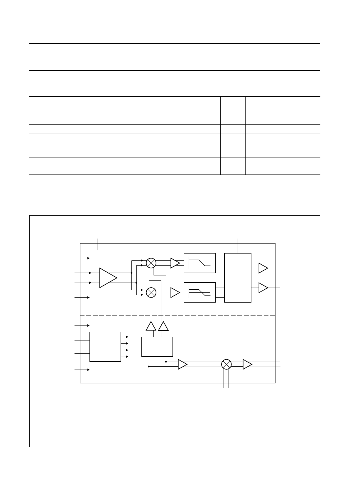
BLOCK DIAGRAM
supply voltage 3.6 3.75 5.3 V
receive supply current 21 26 32 mA
transmit supply current 9 12 15 mA
noise figure on demonstration board (including matching
− 3.6 4.7 dB
and PCB losses)
conversion power gain 19 22 25 dB
operating ambient temperature −30 +25 +75 °C
handbook, full pagewidth
V
CC1
RFINA
RFINB
GND1
V
CC2
RXON
TXON
SXON
GND2
n.c. n.c. SBS
4
5
6
7
15
11
12
REGULATORS
10
16
2 3
LNA
low-noise
amplifier
CURRENT
RX
TX
IF
LO
UAA2073AM
QUADRATURE
PHASE
SHIFTER
+45
+135
o
C
o
C
TRANSMIT SECTION
LOCAL OSCILLATOR
SECTION
LOINA
1
IF
COMBINER
RECEIVE SECTION
MIXER
81718
9
TXINATXINBLOINB
20
19
14
13
MGD149
IFA
IFB
TXOIFA
TXOIFB
Fig.1 Block diagram.
1997 Jan 27 3
Philips Semiconductors Product specification
Image rejecting front-end
for GSM applications
PINNING
SYMBOL PIN DESCRIPTION
SBS 1 sideband selection (should be
grounded for f
LO<fRF
n.c. 2 not connected
n.c. 3 not connected
V
CC1
4 supply voltage for receive and
transmit sections
RFINA 5 RF input A (balanced)
RFINB 6 RF input B (balanced)
GND1 7 ground 1 for receive and transmit
sections
TXINA 8 transmit mixer input A (balanced)
TXINB 9 transmit mixer input B (balanced)
SXON 10 hardware power-on of LO section
(including buffers to RX and TX)
RXON 11 hardware power-on for receive
section and LO buffers to RX
TXON 12 hardware power-on for transmit
section and LO buffers to TX
TXOIFB 13 transmit mixer IF output B
(balanced)
TXOIFA 14 transmit mixer IF output A
(balanced)
V
CC2
15 supply voltage for LO section
GND2 16 ground 2 for LO section
LOINB 17 LO input B (balanced)
LOINA 18 LO input A (balanced)
IFB 19 IF output B (balanced)
IFA 20 IF output A (balanced)
)
handbook, halfpage
UAA2073AM
SBS
1
n.c.
2
n.c.
3
V
4
CC1
RFINA
5
UAA2073AM
6
RFINB
7
GND1
TXINA
8
9
TXINB
10
SXON RXON
Fig.2 Pin configuration.
MGD150
20
19
18
17
16
15
14
13
12
11
IFA
IFB
LOINA
LOINB
GND2
V
CC2
TXOIFA
TXOIFB
TXON
1997 Jan 27 4
Philips Semiconductors Product specification
Image rejecting front-end
for GSM applications
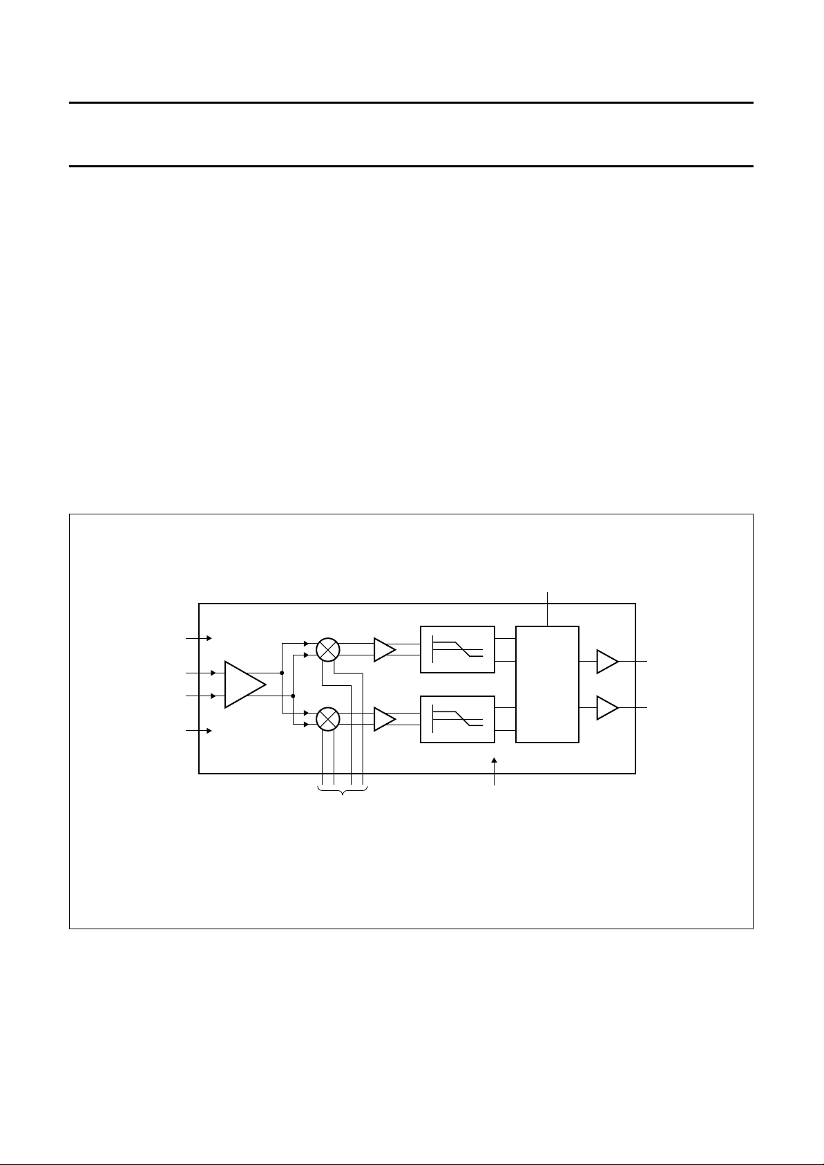
FUNCTIONAL DESCRIPTION
Receive section
The circuit contains a low-noise amplifier followed by two
high dynamic range mixers. These mixers are of the
Gilbert-cell type. The whole internal architecture is fully
differential.
The local oscillator, shifted in phase to 45° and 135°,
mixes the amplified RF to create I and Q channels.
The two I and Q channels are buffered, phase shifted by
45° and 135° respectively, amplified and recombined
internally to realize the image rejection.
Pin SBS allows sideband selection:
• f
LO>fRF
• fLO<fRF (SBS = 0).
Where fRF is the frequency of the wanted signal.
(SBS = 1)
UAA2073AM
Balanced signal interfaces are used for minimizing
crosstalk due to package parasitics. The RF differential
input impedance is 150 Ω (parallel real part), chosen to
minimize current consumption at best noise performance.
The IF output is differential and of the open-collector type,
tuned for 175 MHz. Typical application will load the output
with a 680 Ω resistor load at each IF output, plus a 1 kΩ
load consisting in the input impedance of the IF filter or in
the input impedance of the matching network for the IF
filter. The power gain refers to the available power on this
1kΩ load. The path to V
achieved via tuning inductors. The output voltage is limited
to VCC+3Vbe or 3 diode forward voltage drops.
Fast switching, on/off, of the receive section is controlled
by the hardware input RXON.
for the DC current should be
CC
handbook, full pagewidth
V
CC1
RFINA
RFINB
GND1
LNA
MIXER
MIXER
LOIN
IF
amplifier
IF
amplifier
+45
+135
o
o
RXON
Fig.3 Block diagram, receive section.
SBS
IF
COMBINER
MBH188
IFA
IFB
1997 Jan 27 5
Philips Semiconductors Product specification
Image rejecting front-end
for GSM applications
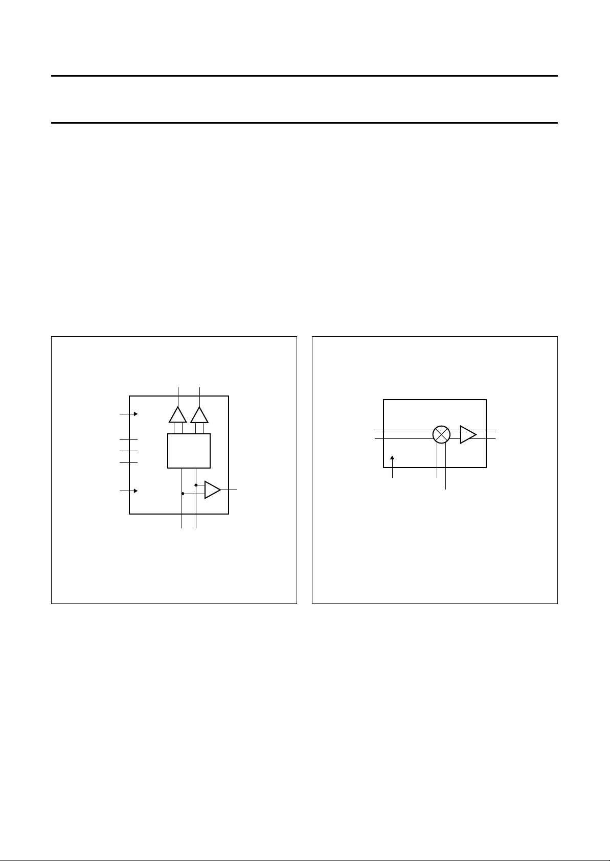
Local oscillator section
The Local Oscillator (LO) input directly drives the two
internal all-pass networks to provide quadrature LO to the
receive mixers.
The LO differential input impedance is 50 Ω (parallel real
part).
A synthesizer-on (SX) mode is used to power-up the
buffering on the LO inputs, minimizing the pulling effect on
the external VCO when entering transmit or receive
modes.
This mode is active when the SXON input is HIGH. Table 1
shows status of circuit in accordance with TXON, RXON
and SXON inputs.
handbook, halfpage
to RX
UAA2073AM
Transmit mixer
This mixer is used for down-conversion to the transmit IF.
Its inputs are coupled to the transmit RF and down-convert
it to a modulated transmit IF frequency which is phase
locked with the baseband modulation.
The transmit mixer provides a differential input at 200 Ω
and a differential output driver buffer for a 1 kΩ load.
The IF outputs are low impedance (emitter followers).
Fast switching, on/off, of the transmit section is controlled
by the hardware input TXON.
V
CC2
RXON
TXON
SXON
GND2
LOINA
QUAD
LOINB
Fig.4 Block diagram, LO section.
to TX
MBH189
handbook, halfpage
LOIN
Fig.5 Block diagram, transmit mixer.
TX MIXER
TXOIFA
TXOIFB
MBH190
TXINBTXON
TXINA
1997 Jan 27 6
 Loading...