

Philips UAA2068G Datasheet

INTEGRATED CIRCUITS
DATA SH EET
UAA2068G
Transmit chain and synthesizer with
integrated VCO for DECT
Product specification
Supersedes data of 1998 Jan 07
File under Integrated Circuits, IC17
1998 Nov 19
Philips Semiconductors Product specification
Transmit chain and synthesizer with
integrated VCO for DECT
FEATURES
• Economical integrated solution for frequency generation
in DECT cordless telephones
• Integrated low phase noise 950 MHz VCO with
frequency doubler
• Local Oscillator (LO) drive (−14 dBm) for RF mixer
circuit
• Dedicated DECT PLL synthesizer
• 3-line serial interface bus
• 3 dBm output preamplifier with an integrated switch
• Low current consumption from 3 V supply
• Compatible with Philips Semiconductors ABC baseband
chip (PCD509x series).
APPLICATIONS
• 1880 to 1920 MHz DECT cordless telephones.
GENERAL DESCRIPTION
The UAA2068G BiCMOS device integrates a 950 MHz
VCO, a frequency doubler, main and reference dividers
and a phase comparator, to implement a phase-locked
loop for DECT channel frequencies. The 1.9 GHz signal is
buffered and switched, in TX mode, to drive the transmit
power amplifier (CGY20xx series) or, in RX mode, to be
used as an LO signal for the receiver mixer IC (UAA2078).
UAA2068G
The reference divider ratio is fixed at 8. Outputs of the
main and reference dividers drive a phase comparator
where a charge pump produces phase error current pulses
for integration in an external loop filter. Only a passive loop
filter is necessary. The charge-pump current (phase
comparator gain) is set by an external resistor at pin R
The VCO is powered from an internally regulated voltage
source and includes internal varicap diodes. Its tuning
range is wider than the required band to allow for
production spreads. In a TDMA system such as DECT, the
VCO and the synthesizer are switched on one slot before
the required one to lock the VCO to the required channel
frequency. Just before the required slot, the synthesizer is
switched off, allowing open-loop modulation of the VCO
during transmission. When opening the loop, the
frequency pulling (due to switching off the synthesizer) can
be maintained within the DECT specification.
The device is designed to operate from 3 NiCd cells in
pocket phones, with low current and nominal 3.6 V
supplies. Separate power and ground pins are provided to
the different parts of the circuit. The ground leads should
be short-circuited externally to prevent large currents
flowing across the die and thus causing damage.
All supply pins (VCC) must also be at the same potential,
except V
other supply pins (e.g. VCC= 3 V and V
wider VCO control voltage range).
which can be equal to or greater than the
CC(CP)
CC(CP)
= 5 V for
SET
.
The synthesizer’s main divider is driven by the frequency
doubler output in the range from 1880 to 1920 MHz and
programmed via a 3-wire serial bus.
ORDERING INFORMATION
TYPE NUMBER
NAME DESCRIPTION VERSION
UAA2068G LQFP32 plastic low profile quad flat package; 32 leads; body 5 × 5 × 1.4 mm SOT401-1
1998 Nov 19 2
PACKAGE
Philips Semiconductors Product specification
Transmit chain and synthesizer with
UAA2068G
integrated VCO for DECT
QUICK REFERENCE DATA
V
= 3.6 V; V
CC
given are not tested.
SYMBOL PARAMETER CONDITIONS MIN. TYP. MAX. UNIT
V
CC
V
CC(CP)
I
CC(SYA)
I
CC(SYD)
I
CC(VCO)
I
CC(BUF)
I
CC(DBL)
I
CC(AMP)
I
CC(pd)
f
o(RF)
f
xtal
f
PC
T
+
+
amb
CC(CP)
= 3.6 V; T
=25°C; unless otherwise specified. Characteristics for which only a typical value is
amb
general supply voltage 3.0 3.6 5.2 V
charge-pump supply voltage V
CC(CP)
≥ V
CC
3.0 3.6 5.2 V
synthesizer supply current S_EN = 1 − 9.5 14 mA
VCO and buffer parts supply current VCO_ON = 1 − 9.5 14 mA
doubler supply current in RX mode − 14.4 19 mA
in TX mode − 10 14 mA
TX preamplifier supply current in RX mode − 050µA
in TX mode − 24 32 mA
total supply current in power-down mode − 550µA
RF output frequency 1880 − 1920 MHz
crystal reference input frequency − 13.824 − MHz
phase comparator frequency − 1728 − kHz
operating ambient temperature −10 − +60 °C
1998 Nov 19 3
Philips Semiconductors Product specification
Transmit chain and synthesizer with
integrated VCO for DECT
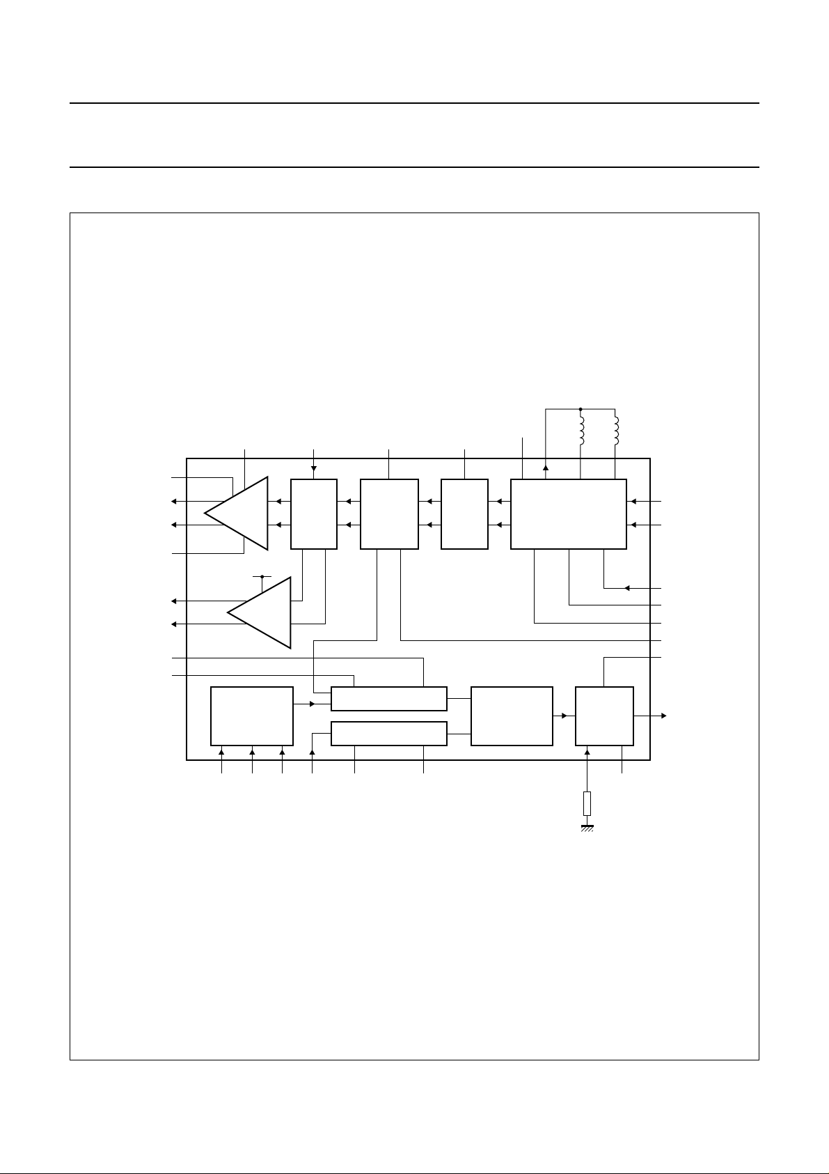
BLOCK DIAGRAM
handbook, full pagewidth
V
R_OFF
AMPGND
V
CC(SYD)
V
CC(SYA)
TXA
TXB
LOA
LOB
26
29
28
27
12
13
2
5
CC(AMP)
30 15 11 16 17 24 21 20
PREAMP
V
CC(DBL)
BUFFER
3-LINE BUS
1 31 4 3 6 10 7
32
T_EN
RF
SWITCH
LO
MAIN DIVIDER
REFERENCE DIVIDER
V
CC(DBL)
DOUBLER
V
CC(BUF)
BUFFER
UAA2068G
COMPARATOR
V
CC(VCO)
PHASE
V
REG
VCO
LL
VCOB
VCOA
23
18
25
22
19
14
CHARGE
PUMP
UAA2068G
V
TUNE
V
MOD
VCO_ON
VCGND
VCOGND
DBLGND
9
V
CC(CP)
8
CP
DATA
CLK
XTAL
SYDGND
SYAGND
S_EN
Fig.1 Block diagram.
1998 Nov 19 4
R
SET
CPGND
R
SET
MGK383
Philips Semiconductors Product specification
Transmit chain and synthesizer with
integrated VCO for DECT
PINNING
SYMBOL PIN DESCRIPTION
DATA 1 3-wire programming bus data input
V
CC(SYD)
SYDGND 3 synthesizer CMOS divider ground
XTAL 4 reference frequency input
V
CC(SYA)
SYAGND 6 synthesizer prescaler ground
CPGND 7 charge-pump ground
CP 8 charge-pump output signal
V
CC(CP)
R
SET
V
CC(DBL)
LOA 12 local oscillator output A
LOB 13 local oscillator output B
DBLGND 14 doubler ground
T_EN 15 transmit enable signal input
V
CC(BUF)
V
CC(VCO)
V
MOD
VCOGND 19 VCO ground; note 1
VCOA 20 VCO inductor connection A
VCOB 21 VCO inductor connection B
VCGND 22 internal varicap ground; note 1
V
TUNE
V
REG
VCO_ON 25 VCO power on control input; note 2
R_OFF 26 power on control for RX LO buffer/TX preamplifier; note 3
AMPGND 27 transmit amplifier ground
TXB 28 transmit amplifier output B
TXA 29 transmit amplifier output A
V
CC(AMP)
CLK 31 3-wire programming bus clock input
S_EN 32 synthesizer enable signal input
2 synthesizer CMOS divider positive supply voltage
5 synthesizer prescaler positive supply voltage
9 charge-pump positive supply voltage
10 charge-pump current setting input
11 doubler positive supply voltage
16 VCO isolation buffer positive supply voltage
17 VCO positive supply voltage
18 transmit modulation input
23 VCO tuning input
24 VCO regulator output
30 transmit amplifier positive supply voltage
UAA2068G
Notes
1. Pins 19 and 22 are internally short-circuited.
2. Use with S_PWR on ABC baseband chip.
3. Use with R_PWR on ABC baseband chip.
1998 Nov 19 5
Philips Semiconductors Product specification
Transmit chain and synthesizer with
integrated VCO for DECT
handbook, full pagewidth
CLK
S_EN
31
32
1
DATA
XTAL
CP
2
3
4
5
6
7
8
9
10
SET
R
CC(CP)
V
V
CC(SYD)
SYDGND
V
CC(SYA)
SYAGND
CPGND
CC(AMP)
V
TXA
30
29
UAA2068G
11
12
LOA
CC(DBL)
V
TXB
28
13
LOB
R_OFF
AMPGND
27
26
14
15
T_EN
DBLGND
VCO_ON
25
24
23
22
21
20
19
18
17
16
CC(BUF)
V
V
REG
V
TUNE
VCGND
VCOB
VCOA
VCOGND
V
MOD
V
CC(VCO)
MGK382
UAA2068G
Fig.2 Pin configuration.
FUNCTIONAL DESCRIPTION
Transmit chain
BUFFER AND FREQUENCY DOUBLER
VCO,
The VCO operates at a nominal centre frequency of
950 MHz. It is fully integrated apart from two inductors
which complete the resonator network. This VCO operates
from an on-chip regulated power supply (V
REG
), which
minimizes frequency disturbances due to variations in
supply voltage. The buffered VCO signal is fed into a
frequency doubler. The large difference between the
transmitted and VCO frequencies reduces
transmitter-oscillator coupling problems.
The output of the doubler is used to drive the synthesizer
main divider and can also be switched to either the TX
preamplifier or the RX LO output buffer. The high isolation
obtained from the VCO buffer and the frequency doubler
ensures very small frequency changes when turning on
the TX preamplifier or the RX LO output buffer. In TX
mode, the oscillator can be directly modulated with GMSK
filtered data at pin V
MOD
.
RF
SWITCH
The RF switch passes the doubled VCO signal to either
the TX preamplifier (when T_EN is HIGH) or to the RX LO
buffer (when T_EN is LOW). In TX mode, the difference in
the RF power levels, observed at the TX output when
T_EN is switched from LOW-to-HIGH, is typically 40 dB.
TX
PREAMPLIFIER
The TX preamplifier amplifies the RF signal up to a level of
3 dBm which is suitable for use with Philips
Semiconductors DECT power amplifiers such as the
CGY20xx series. It is powered-up when both R_OFF and
VCO_ON are HIGH.
RX LO
BUFFER
The RX LO buffer outputs the frequency doubled VCO
signal at a level of −14 dBm. This signal can then be used
as the local oscillator drive for the receive mixers of
devices such as the UAA2078. The buffer is powered-up
when R_OFF is LOW and VCO_ON is HIGH.
1998 Nov 19 6
 Loading...