

Philips TPS2.1LLA Service Manual

Color Television Chassis
18290_000_090310.eps
090415
TPS2.1L
LA
Contents Page Contents Page
1. Revision List 2
2. Technical Specifications and Connections 2
3. Precautions, Notes, and Abbreviation List 6
4. Mechanical Instructions 10
5. Service Modes, Error Codes, and Fault Finding 14
6. Alignments 16
7. Circuit Descriptions 18
8. IC Data Sheets 22
9. Block Diagrams
Wiring Diagram 22" 29
Wiring Diagram 26" 30
Block Diagram 22" 31
Block Diagram -1 26" 32
Block Diagram -2 26" 33
Power Management 22" 34
Power Management 26" 35
10. Circuit Diagrams and PWB Layouts Drawing PWB
Power board: Adapter, 22"
Power Board: Inverter, 22" (A02) 37 38-39
Power board: Adapter, 26" (A01) 40 42-43
Power board: Inverter, 26" (A02) 41 42-43
SSB 22": D-SUB Input (B01) 44 60-65
SSB 22": Video Input and CVBS Output (B02) 45 60-65
SSB 22": SCART (B03) 46 60-65
SSB 22": Tuner (B04) 47 60-65
SSB 22": HDMI Output (B05) 48 60-65
SSB 22": LIPS & Inverter I/F (B06) 49 60-65
SSB 22": Scaler MST9A885GL - LF (B07) 50 60-65
SSB 22": WT6703F (Standby MCU) (B08) 51 60-65
SSB 22": Flash ROM and Memory (B09) 52 60-65
SSB 22": Key, IR BD & Compair I/F (B10) 53 60-65
SSB 22": Panel I/F (B11) 54 60-65
SSB 22": ITV I/F and AOC Hotel (B12) 55 60-65
SSB 22": USB (B13) 56 60-65
©
Copyright 2009 Koninklijke Philips N.V.
All rights reserved. No part of this publication may be reproduced, stored in a
retrieval system or transmitted, in any form or by any means, electronic, mechanical,
photocopying, or otherwise without the prior permission of Philips.
(A01) 36 38-39
SSB 22": Audio /AMP (B14) 57 60-65
SSB 22": Audio I/F and S/PDIF Out (B15) 58 60-65
SSB 22": DC -DC Power (B16) 59 60-65
SSB 26": D-SUB Input (B16) 70 87-92
SSB 26": Video Input and CVBS Output (B16) 71 87-92
SSB 26": SCART (B16) 72 87-92
SSB 26": Tuner (B16) 73 87-92
SSB 26": HDMI Input 1 (B16) 74 87-92
SSB 26": HDMI Input 2 (B16) 75 87-92
SSB 26": LIPS & Inverter I/F (B07) 76 87-92
SSB 26": Scaler MST9A885GL -LQFP256 (B08) 77 87-92
SSB 26": WT6703F Standby MCU (B09) 78 87-92
SSB 26": Flash ROM and Memory (B10) 79 87-92
SSB 26": Key, IR BD & ComPair I/F (B11) 80 87-92
SSB 26": Panel I/F (B12) 81 87-92
SSB 26": iTV I/F and AOC Hotel (B13) 82 87-92
SSB 26": USB (B14) 83 87-92
SSB 26": Audio/Amplifier (B15) 84 87-92
SSB 26": Audio I/F and S/PDIF Out (B16) 85 87-92
SSB 26": DC - DC Power (B17) 86 87-92
IR Board (J) 97 98
Keyboard control panel (E) 99 100
Published by QM/JY 0966 BU TV Consumer Care Printed in the Netherlands Subject to modification EN 3122 785 18270
2010-Jun-18
EN 2 TPS2.1L LA1.
Revision List
1. Revision List
Manual xxxx xxx xxxx0
• First release.
2. Technical Specifications and Connections
Index of this chapter:
2.1
Technical Specifications
2.2 Directions for Use
2.3 Connections
2.4 Chassis Overview
Notes:
• Figures can deviate due to the different set executions.
• Specifications are indicative (subject to change).
2.1 Technical Specifications
For on-line product support please use the links in. Here is
product information available, as well as getting started, user
manuals, frequently asked questions and software & drivers.
Table 2-1 Described Model Numbers:
Model Number Styling Published in:
22PFL3404/77
22PFL3404/78
26PFL3404/77
26PFL3404/78
Note: The given Model Numbers are subject to change.
Click 3122 785 18270
2.2 Directions for Use
Click on the hyperlinks in table above.
2010-Jun-18
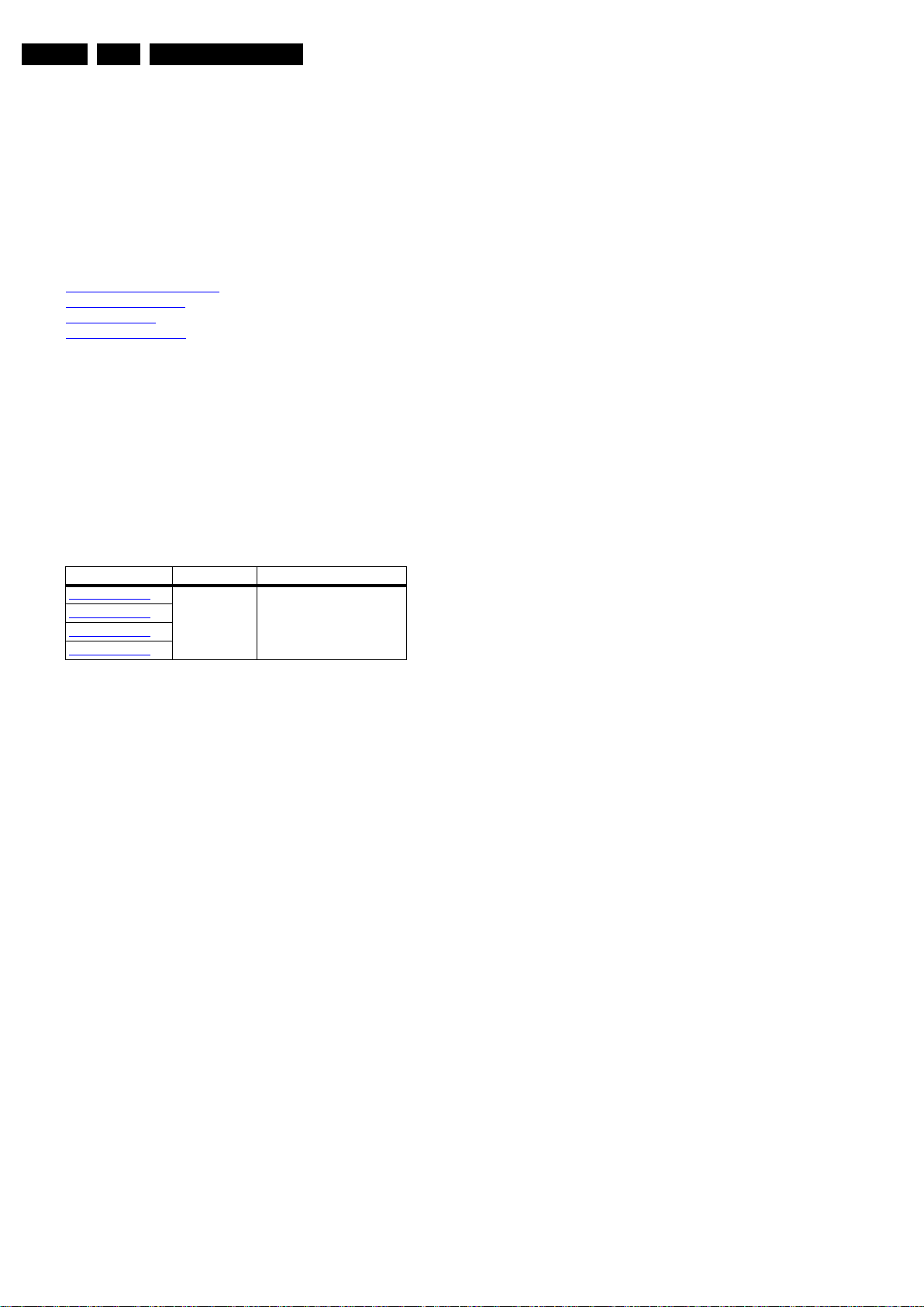
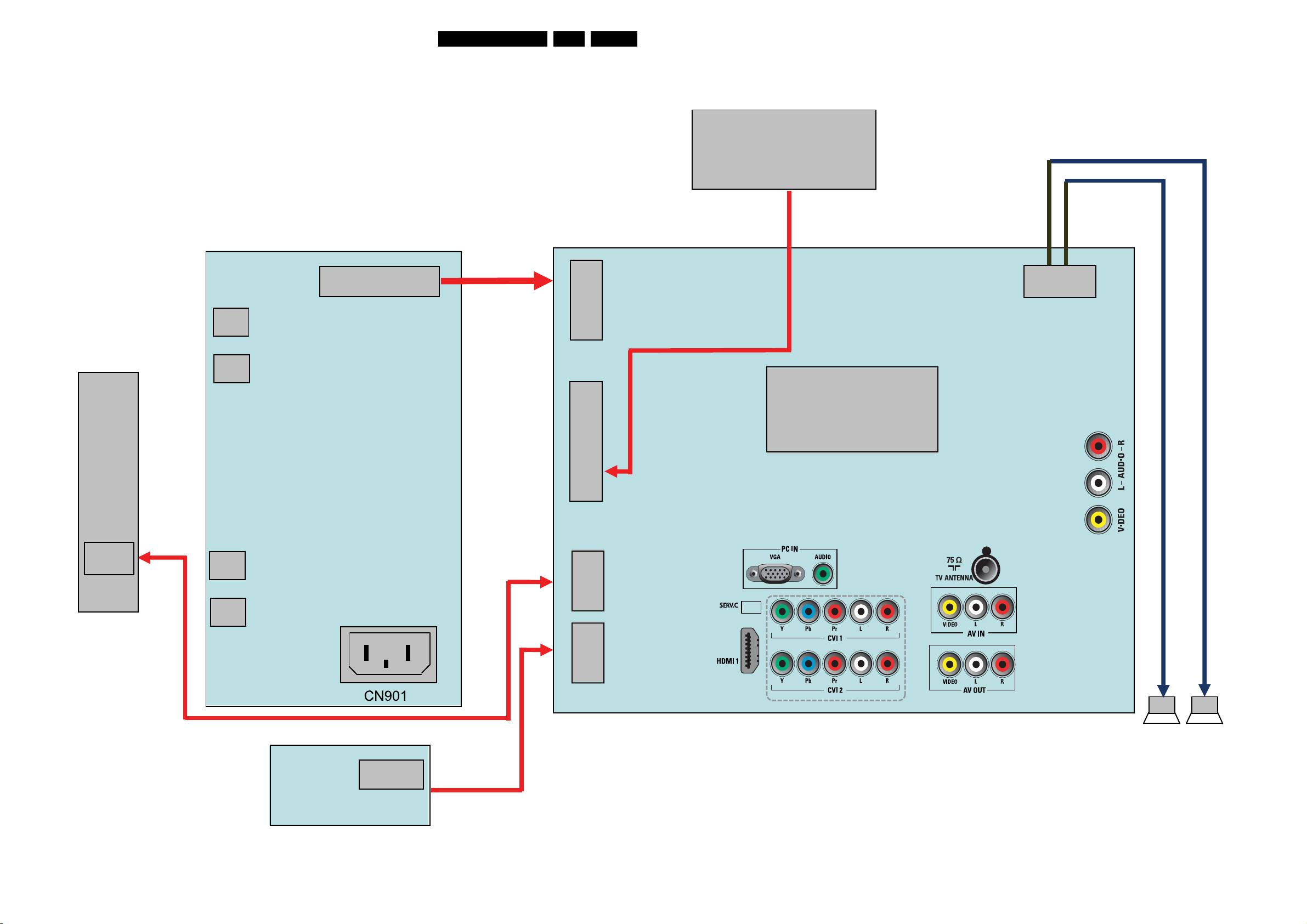
2.3 Connections
18270_002_090531.eps
090611
5
9
10
11
6
7
8
SERV.C
2
3
Technical Specifications and Connections
EN 3TPS2.1L LA 2.
Figure 2-1 Connection overview 22"
2010-Jun-18

EN 4 TPS2.1L LA2.
SERV.CSERV.C
18270_001_090529.eps
090611
2
3
1
4
56
7
11
8
9
10
Technical Specifications and Connections
Figure 2-2 Connection overview 26"
Note: The following connector color abbreviations are used
(acc. to DIN/IEC 757): Bk= Black, Bu= Blue, Gn= Green,
Gy= Grey, Rd= Red, Wh= White, Ye= Yellow.
2.3.1 Side Connections
1 - Mini Jack: Audio Head phone - Out
Bk - Head phone 32 - 600 ohm / 10 mW ot
2 - Cinch: Audio - In
Rd - Audio R 0.5 V
Wh - Audio L 0.5 V
2010-Jun-18
/ 10 kohm jq
RMS
/ 10 kohm jq
RMS
3 - Cinch: Video CVBS - In, Audio - In
Ye - Video CVBS 1 V
/ 75 ohm jq
PP
Technical Specifications and Connections
10000_017_090121.eps
090428
19
1
18 2
1
6
10
11
5
15
10000_002_090121.eps
090127
EN 5TPS2.1L LA 2.
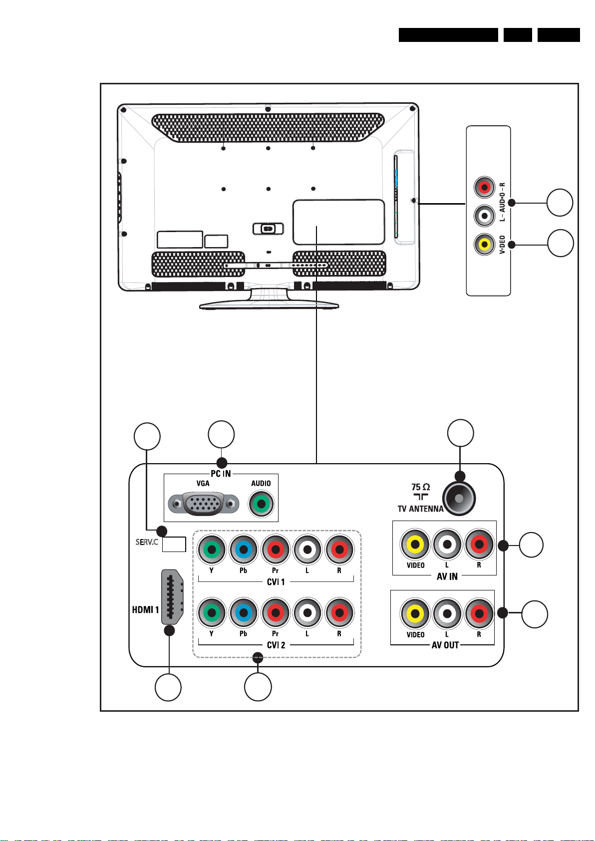
4 - HDMI 1: Digital Video, Digital Audio - In
Figure 2-3 HDMI (type A) connector
1 - D2+ Data channel j
2 - Shield Gnd H
3 - D2- Data channel j
4 - D1+ Data channel j
5 - Shield Gnd H
6 - D1- Data channel j
7 - D0+ Data channel j
8 - Shield Gnd H
9 - D0- Data channel j
10 - CLK+ Data channel j
11 - Shield Gnd H
12 - CLK- Data channel j
13 - Easylink Control channel jk
14 - n.c.
15 - DDC_SCL DDC clock j
16 - DDC_SDA DDC data jk
17 - Ground Gnd H
18 - +5V j
19 - HPD Hot Plug Detect j
20 - Ground Gnd H
2.3.2 Rear Connections
5 - SERV.C
1 - Ground Gnd H
2 - UART_TX Transmit k
3 - UART_RX Receive j
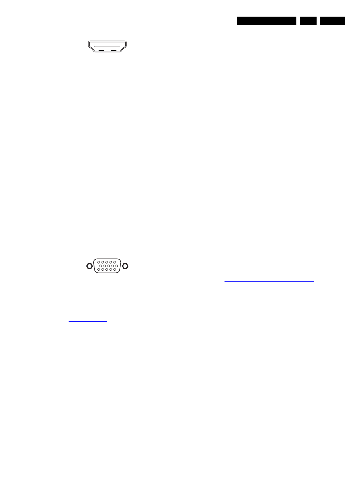
6 - PC IN:VGA
1 - Video Red 0.7 V
2 - Video Green 0.7 V
3 - Video Blue 0.7 V
4-n.c.
/ 75 ohm j
PP
/ 75 ohm j
PP
/ 75 ohm j
PP
5 - Ground Gnd H
6 - Ground Red Gnd H
7 - Ground Green Gnd H
8 - Ground Blue Gnd H
9-+5V
10 - Ground Sync Gnd H
+5 V j
DC
11 - n.c.
12 - DDC_SDA DDC data j
13 - H-sync 0 - 5 V j
14 - V-sync 0 - 5 V j
15 - DDC_SCL DDC clock j
6 - PC IN: Audio - In
Gn - Video - Y 1 V
/ 75 ohm jq
PP
7 - TV ANTENNA - In
- IEC-type (EU) Coax, 75 Ω D
8 - AV Out: Video - Out, Audio - Out
Ye - Video 1 V
Wh - Audio - L 0.5 V
Rd - Audio - R 0.5 V
/ 75 ohm jq
PP
/ 10 kohm jq
RMS
/ 10 kohm jq
RMS
9 - AV IN: Video - In, Audio - In
Ye - Video 1 V
Wh - Audio - L 0.5 V
Rd - Audio - R 0.5 V
/ 75 ohm jq
PP
/ 10 kohm jq
RMS
/ 10 kohm jq
RMS
10 - CVI1/CVI2: YPbPr - In, Audio - In
Gn - Video - Y 1 V
Bu - Video - Pb 0.7 V
Rd - Video - Pr 0.7 V
Wh - Audio - L 0.5 V
Rd - Audio - R 0.5 V
/ 75 ohm jq
PP
/ 75 ohm jq
PP
/ 75 ohm jq
PP
/ 10 kohm jq
RMS
/ 10 kohm jq
RMS
Figure 2-4 VGA connector
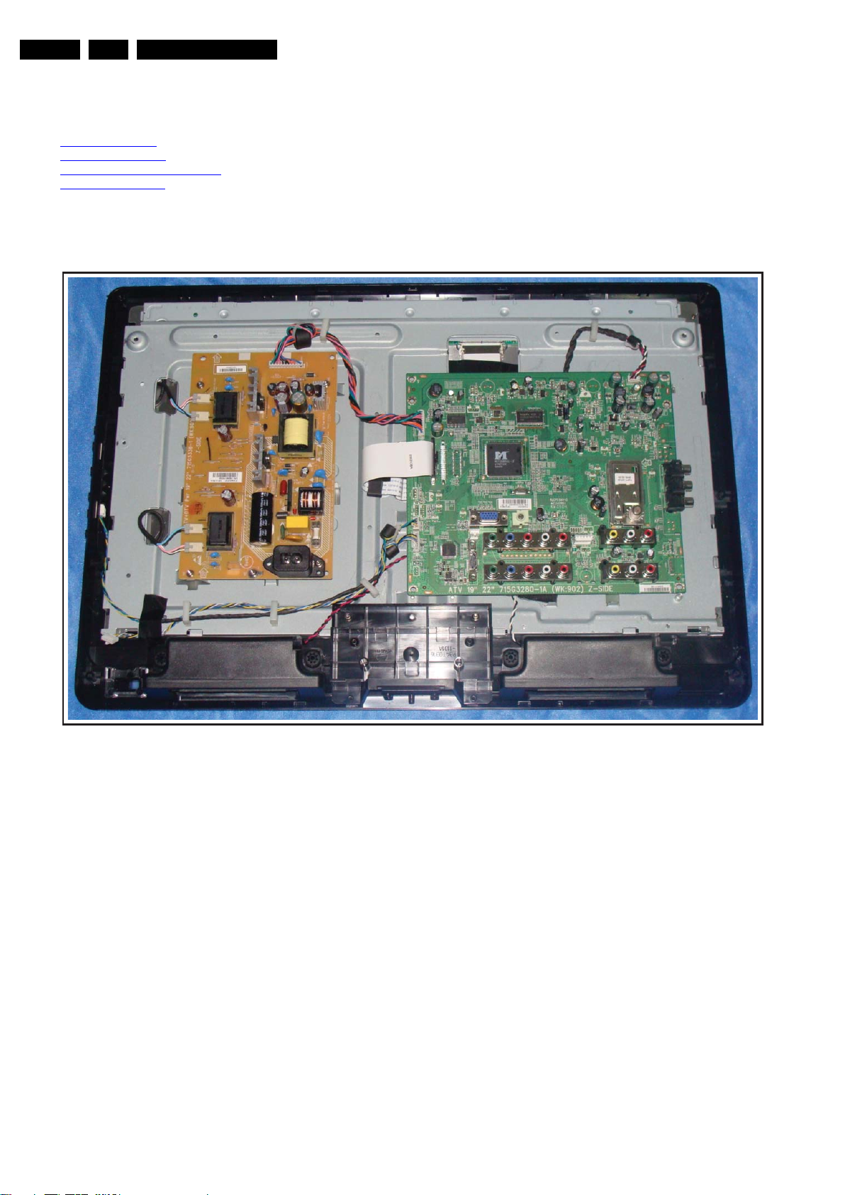
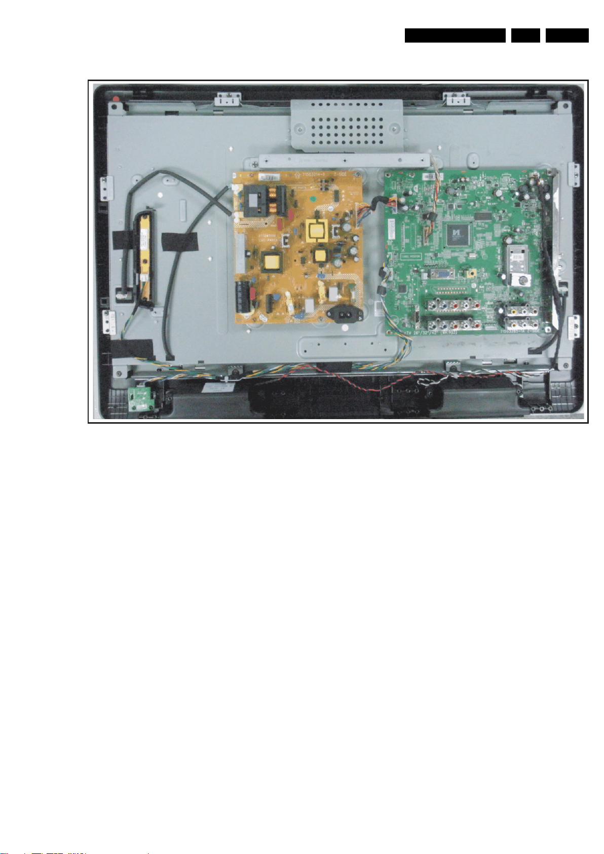
2.4 Chassis Overview
Refer to 9. Block Diagrams for PWB/CBA locations.
11 - HDMI 1: Digital Video, Digital Audio - In
See 4 - HDMI 1: Digital Video, Digital Audio - In
.
2010-Jun-18

EN 6 TPS2.1L LA3.
Precautions, Notes, and Abbreviation List
3. Precautions, Notes, and Abbreviation List
Index of this chapter:
3.1
Safety Instructions
3.2 Warnings
3.3 Notes
3.4 Abbreviation List
3.1 Safety Instructions
Safety regulations require the following during a repair:
• Connect the set to the Mains/AC Power via an isolation
transformer (> 800 VA).
• Replace safety components, indicated by the symbol h,
only by components identical to the original ones. Any
other component substitution (other than original type) may
increase risk of fire or electrical shock hazard.
Safety regulations require that after a repair, the set must be
returned in its original condition. Pay in particular attention to
the following points:
• Route the wire trees correctly and fix them with the
mounted cable clamps.
• Check the insulation of the Mains/AC Power lead for
external damage.
• Check the strain relief of the Mains/AC Power cord for
proper function.
• Check the electrical DC resistance between the Mains/AC
Power plug and the secondary side (only for sets that have
a Mains/AC Power isolated power supply):
1. Unplug the Mains/AC Power cord and connect a wire
between the two pins of the Mains/AC Power plug.
2. Set the Mains/AC Power switch to the “on” position
(keep the Mains/AC Power cord unplugged!).
3. Measure the resistance value between the pins of the
Mains/AC Power plug and the metal shielding of the
tuner or the aerial connection on the set. The reading
should be between 4.5 MΩ and 12 MΩ.
4. Switch “off” the set, and remove the wire between the
two pins of the Mains/AC Power plug.
• Check the cabinet for defects, to prevent touching of any
inner parts by the customer.
• Where necessary, measure the waveforms and voltages
with (D) and without (E) aerial signal. Measure the
voltages in the power supply section both in normal
operation (G) and in stand-by (F). These values are
indicated by means of the appropriate symbols.
3.3.2 Schematic Notes
• All resistor values are in ohms, and the value multiplier is
often used to indicate the decimal point location (e.g. 2K2
indicates 2.2 kΩ).
• Resistor values with no multiplier may be indicated with
either an “E” or an “R” (e.g. 220E or 220R indicates 220 Ω).
• All capacitor values are given in micro-farads (μ=× 10
nano-farads (n =× 10
• Capacitor values may also use the value multiplier as the
decimal point indication (e.g. 2p2 indicates 2.2 pF).
• An “asterisk” (*) indicates component usage varies. Refer
to the diversity tables for the correct values.
• The correct component values are listed on the Philips
Spare Parts Web Portal.
3.3.3 Spare Parts
For the latest spare part overview, consult your Philips Spare
Part web portal.
3.3.4 BGA (Ball Grid Array) ICs
Introduction
For more information on how to handle BGA devices, visit this
URL: http://www.atyourservice-magazine.com
“Magazine”, then go to “Repair downloads”. Here you will find
Information on how to deal with BGA-ICs.
BGA Temperature Profiles
For BGA-ICs, you must use the correct temperature-profile.
Where applicable and available, this profile is added to the IC
Data Sheet information section in this manual.
-9
), or pico-farads (p =× 10
. Select
-12
-6
),
).
3.2 Warnings
• All ICs and many other semiconductors are susceptible to
electrostatic discharges (ESD w). Careless handling
during repair can reduce life drastically. Make sure that,
during repair, you are connected with the same potential as
the mass of the set by a wristband with resistance. Keep
components and tools also at this same potential.
• Be careful during measurements in the high voltage
section.
• Never replace modules or other components while the unit
is switched “on”.
• When you align the set, use plastic rather than metal tools.
This will prevent any short circuits and the danger of a
circuit becoming unstable.
3.3 Notes
3.3.1 General
• Measure the voltages and waveforms with regard to the
chassis (= tuner) ground (H), or hot ground (I), depending
on the tested area of circuitry. The voltages and waveforms
shown in the diagrams are indicative. Measure them in the
Service Default Mode with a colour bar signal and stereo
sound (L: 3 kHz, R: 1 kHz unless stated otherwise) and
picture carrier at 475.25 MHz for PAL, or 61.25 MHz for
NTSC (channel 3).
2010-Jun-18
3.3.5 Lead-free Soldering
Due to lead-free technology some rules have to be respected
by the workshop during a repair:
• Use only lead-free soldering tin. If lead-free solder paste is
required, please contact the manufacturer of your soldering
equipment. In general, use of solder paste within
workshops should be avoided because paste is not easy to
store and to handle.
• Use only adequate solder tools applicable for lead-free
soldering tin. The solder tool must be able:
– To reach a solder-tip temperature of at least 400°C.
– To stabilize the adjusted temperature at the solder-tip.
– To exchange solder-tips for different applications.
• Adjust your solder tool so that a temperature of around
360°C - 380°C is reached and stabilized at the solder joint.
Heating time of the solder-joint should not exceed ~ 4 sec.
Avoid temperatures above 400°C, otherwise wear-out of
tips will increase drastically and flux-fluid will be destroyed.
To avoid wear-out of tips, switch “off” unused equipment or
reduce heat.
• Mix of lead-free soldering tin/parts with leaded soldering
tin/parts is possible but PHILIPS recommends strongly to
avoid mixed regimes. If this cannot be avoided, carefully
clear the solder-joint from old tin and re-solder with new tin.
3.3.6 Alternative BOM identification
It should be noted that on the European Service website,
“Alternative BOM” is referred to as “Design variant”.
Precautions, Notes, and Abbreviation List
EN 7TPS2.1L LA 3.
The third digit in the serial number (example:
AG2B0335000001) indicates the number of the alternative
B.O.M. (Bill Of Materials) that has been used for producing the
specific TV set. In general, it is possible that the same TV
model on the market is produced with e.g. two different types
of displays, coming from two different suppliers. This will then
result in sets which have the same CTN (Commercial Type
Number; e.g. 28PW9515/12) but which have a different B.O.M.
number.
By looking at the third digit of the serial number, one can
identify which B.O.M. is used for the TV set he is working with.
If the third digit of the serial number contains the number “1”
(example: AG1B033500001), then the TV set has been
manufactured according to B.O.M. number 1. If the third digit is
a “2” (example: AG2B0335000001), then the set has been
produced according to B.O.M. no. 2. This is important for
ordering the correct spare parts!
For the third digit, the numbers 1...9 and the characters A...Z
can be used, so in total: 9 plus 26= 35 different B.O.M.s can be
indicated by the third digit of the serial number.
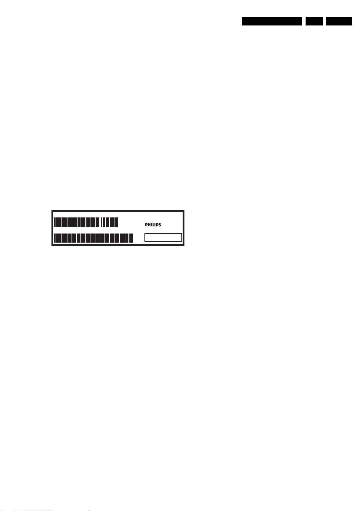
Identification: The bottom line of a type plate gives a 14-digit
serial number. Digits 1 and 2 refer to the production centre (e.g.
AG is Bruges), digit 3 refers to the B.O.M. code, digit 4 refers
to the Service version change code, digits 5 and 6 refer to the
production year, and digits 7 and 8 refer to production week (in
example below it is 2006 week 17). The 6 last digits contain the
serial number.
MODEL :
PROD.NO:
32PF9968/10
AG 1A0617 000001
MADE IN BELGIUM
220-240V 50/60Hz
VHF+S+H+UHF
S
10000_024_090121.eps
~
BJ3.0E LA
Figure 3-1 Serial number (example)
3.3.7 Board Level Repair (BLR) or Component Level Repair (CLR)
If a board is defective, consult your repair procedure to decide
if the board has to be exchanged or if it should be repaired on
component level.
If your repair procedure says the board should be exchanged
completely, do not solder on the defective board. Otherwise, it
cannot be returned to the O.E.M. supplier for back charging!
3.3.8 Practical Service Precautions
• It makes sense to avoid exposure to electrical shock.
While some sources are expected to have a possible
dangerous impact, others of quite high potential are of
limited current and are sometimes held in less regard.
• Always respect voltages. While some may not be
dangerous in themselves, they can cause unexpected
reactions that are best avoided. Before reaching into a
powered TV set, it is best to test the high voltage insulation.
It is easy to do, and is a good service precaution.
128W
100105
3.4 Abbreviation List
0/6/12 SCART switch control signal on A/V
board. 0 = loop through (AUX to TV),
6 = play 16 : 9 format, 12 = play 4 : 3
format
AARA Automatic Aspect Ratio Adaptation:
algorithm that adapts aspect ratio to
remove horizontal black bars; keeps
the original aspect ratio
ACI Automatic Channel Installation:
algorithm that installs TV channels
directly from a cable network by
means of a predefined TXT page
ADC Analogue to Digital Converter
AFC Automatic Frequency Control: control
signal used to tune to the correct
frequency
AGC Automatic Gain Control: algorithm that
controls the video input of the feature
box
AM Amplitude Modulation
AP Asia Pacific
AR Aspect Ratio: 4 by 3 or 16 by 9
ASF Auto Screen Fit: algorithm that adapts
aspect ratio to remove horizontal black
bars without discarding video
information
ATSC Advanced Television Systems
Committee, the digital TV standard in
the USA
ATV See Auto TV
Auto TV A hardware and software control
system that measures picture content,
and adapts image parameters in a
dynamic way
AV External Audio Video
AVC Audio Video Controller
AVIP Audio Video Input Processor
B/G Monochrome TV system. Sound
carrier distance is 5.5 MHz
BDS Business Display Solutions (iTV)
BLR Board-Level Repair
BTSC Broadcast Television Standard
Committee. Multiplex FM stereo sound
system, originating from the USA and
used e.g. in LATAM and AP-NTSC
countries
B-TXT Blue TeleteXT
C Centre channel (audio)
CEC Consumer Electronics Control bus:
remote control bus on HDMI
connections
CL Constant Level: audio output to
connect with an external amplifier
CLR Component Level Repair
ComPair Computer aided rePair
CP Connected Planet / Copy Protection
CSM Customer Service Mode
CTI Color Transient Improvement:
manipulates steepness of chroma
transients
CVBS Composite Video Blanking and
Synchronization
DAC Digital to Analogue Converter
DBE Dynamic Bass Enhancement: extra
low frequency amplification
DCM Data Communication Module. Also
referred to as System Card or
Smartcard (for iTV).
DDC See “E-DDC”
D/K Monochrome TV system. Sound
carrier distance is 6.5 MHz
DFI Dynamic Frame Insertion
2010-Jun-18

EN 8 TPS2.1L LA3.
Precautions, Notes, and Abbreviation List
DFU Directions For Use: owner's manual
DMR Digital Media Reader: card reader
DMSD Digital Multi Standard Decoding
DNM Digital Natural Motion
DNR Digital Noise Reduction: noise
reduction feature of the set
DRAM Dynamic RAM
DRM Digital Rights Management
DSP Digital Signal Processing
DST Dealer Service Tool: special remote
control designed for service
technicians
DTCP Digital Transmission Content
Protection; A protocol for protecting
digital audio/video content that is
traversing a high speed serial bus,
such as IEEE-1394
DVB-C Digital Video Broadcast - Cable
DVB-T Digital Video Broadcast - Terrestrial
DVD Digital Versatile Disc
DVI(-d) Digital Visual Interface (d= digital only)
E-DDC Enhanced Display Data Channel
(VESA standard for communication
channel and display). Using E-DDC,
the video source can read the EDID
information form the display.
EDID Extended Display Identification Data
(VESA standard)
EEPROM Electrically Erasable and
Programmable Read Only Memory
EMI Electro Magnetic Interference
EPG Electronic Program Guide
EPLD Erasable Programmable Logic Device
EU Europe
EXT EXTernal (source), entering the set by
SCART or by cinches (jacks)
FDS Full Dual Screen (same as FDW)
FDW Full Dual Window (same as FDS)
FLASH FLASH memory
FM Field Memory or Frequency
Modulation
FPGA Field-Programmable Gate Array
FTV Flat TeleVision
Gb/s Giga bits per second
G-TXT Green TeleteXT
H H_sync to the module
HD High Definition
HDD Hard Disk Drive
HDCP High-bandwidth Digital Content
Protection: A “key” encoded into the
HDMI/DVI signal that prevents video
data piracy. If a source is HDCP coded
and connected via HDMI/DVI without
the proper HDCP decoding, the
picture is put into a “snow vision” mode
or changed to a low resolution. For
normal content distribution the source
and the display device must be
enabled for HDCP “software key”
decoding.
HDMI High Definition Multimedia Interface
HP HeadPhone
I Monochrome TV system. Sound
2
I
C Inter IC bus
2
I
D Inter IC Data bus
2
I
S Inter IC Sound bus
carrier distance is 6.0 MHz
IF Intermediate Frequency
IR Infra Red
IRQ Interrupt Request
ITU-656 The ITU Radio communication Sector
(ITU-R) is a standards body
subcommittee of the International
Telecommunication Union relating to
radio communication. ITU-656 (a.k.a.
SDI), is a digitized video format used
for broadcast grade video.
Uncompressed digital component or
digital composite signals can be used.
The SDI signal is self-synchronizing,
uses 8 bit or 10 bit data words, and has
a maximum data rate of 270 Mbit/s,
with a minimum bandwidth of 135
MHz.
ITV Institutional TeleVision; TV sets for
hotels, hospitals etc.
LS Last Status; The settings last chosen
by the customer and read and stored
in RAM or in the NVM. They are called
at start-up of the set to configure it
according to the customer's
preferences
LATAM Latin America
LCD Liquid Crystal Display
LED Light Emitting Diode
L/L' Monochrome TV system. Sound
carrier distance is 6.5 MHz. L' is Band
I, L is all bands except for Band I
LPL LG.Philips LCD (supplier)
LS Loudspeaker
LVDS Low Voltage Differential Signalling
Mbps Mega bits per second
M/N Monochrome TV system. Sound
carrier distance is 4.5 MHz
MHEG Part of a set of international standards
related to the presentation of
multimedia information, standardised
by the Multimedia and Hypermedia
Experts Group. It is commonly used as
a language to describe interactive
television services
MIPS Microprocessor without Interlocked
Pipeline-Stages; A RISC-based
microprocessor
MOP Matrix Output Processor
MOSFET Metal Oxide Silicon Field Effect
Transistor, switching device
MPEG Motion Pictures Experts Group
MPIF Multi Platform InterFace
MUTE MUTE Line
MTV Mainstream TV: TV-mode with
Consumer TV features enabled (iTV)
NC Not Connected
NICAM Near Instantaneous Compounded
Audio Multiplexing. This is a digital
sound system, mainly used in Europe.
NTC Negative Temperature Coefficient,
non-linear resistor
NTSC National Television Standard
Committee. Color system mainly used
in North America and Japan. Color
carrier NTSC M/N= 3.579545 MHz,
NTSC 4.43= 4.433619 MHz (this is a
VCR norm, it is not transmitted off-air)
NVM Non-Volatile Memory: IC containing
TV related data such as alignments
O/C Open Circuit
OSD On Screen Display
OAD Over the Air Download. Method of
software upgrade via RF transmission.
Upgrade software is broadcasted in
TS with TV channels.
OTC On screen display Teletext and
Control; also called Artistic (SAA5800)
P50 Project 50: communication protocol
between TV and peripherals
PAL Phase Alternating Line. Color system
mainly used in West Europe (color
carrier= 4.433619 MHz) and South
America (color carrier PAL M=
2010-Jun-18

Precautions, Notes, and Abbreviation List
EN 9TPS2.1L LA 3.
3.575612 MHz and PAL N= 3.582056
MHz)
PCB Printed Circuit Board (same as “PWB”)
PCM Pulse Code Modulation
PDP Plasma Display Panel
PFC Power Factor Corrector (or Pre-
conditioner)
PIP Picture In Picture
PLL Phase Locked Loop. Used for e.g.
FST tuning systems. The customer
can give directly the desired frequency
POD Point Of Deployment: a removable
CAM module, implementing the CA
system for a host (e.g. a TV-set)
POR Power On Reset, signal to reset the uP
PSDL Power Supply for Direct view LED
backlight with 2D-dimming
PSL Power Supply with integrated LED
drivers
PSLS Power Supply with integrated LED
drivers with added Scanning
functionality
PTC Positive Temperature Coefficient,
non-linear resistor
PWB Printed Wiring Board (same as “PCB”)
PWM Pulse Width Modulation
QRC Quasi Resonant Converter
QTNR Quality Temporal Noise Reduction
QVCP Quality Video Composition Processor
RAM Random Access Memory
RGB Red, Green, and Blue. The primary
color signals for TV. By mixing levels
of R, G, and B, all colors (Y/C) are
reproduced.
RC Remote Control
RC5 / RC6 Signal protocol from the remote
control receiver
RESET RESET signal
ROM Read Only Memory
RSDS Reduced Swing Differential Signalling
data interface
R-TXT Red TeleteXT
SAM Service Alignment Mode
S/C Short Circuit
SCART Syndicat des Constructeurs
d'Appareils Radiorécepteurs et
Téléviseurs
SCL Serial Clock I
SCL-F CLock Signal on Fast I
SD Standard Definition
SDA Serial Data I
SDA-F DAta Signal on Fast I
2
C
2
C bus
2
C
2
C bus
SDI Serial Digital Interface, see “ITU-656”
SDRAM Synchronous DRAM
SECAM SEequence Couleur Avec Mémoire.
Color system mainly used in France
and East Europe. Color carriers=
4.406250 MHz and 4.250000 MHz
SIF Sound Intermediate Frequency
SMPS Switched Mode Power Supply
SoC System on Chip
SOG Sync On Green
SOPS Self Oscillating Power Supply
SPI Serial Peripheral Interface bus; a 4-
wire synchronous serial data link
standard
S/PDIF Sony Philips Digital InterFace
SRAM Static RAM
SRP Service Reference Protocol
SSB Small Signal Board
SSC Spread Spectrum Clocking, used to
reduce the effects of EMI
STB Set Top Box
STBY STand-BY
SVGA 800 × 600 (4:3)
SVHS Super Video Home System
SW Software
SWAN Spatial temporal Weighted Averaging
Noise reduction
SXGA 1280 × 1024
TFT Thin Film Transistor
THD Total Harmonic Distortion
TMDS Transmission Minimized Differential
Signalling
TS Transport Stream
TXT TeleteXT
TXT-DW Dual Window with TeleteXT
UI User Interface
uP Microprocessor
UXGA 1 600 × 1 200 (4:3)
V V-sync to the module
VESA Video Electronics Standards
Association
VGA 640 × 480 (4:3)
VL Variable Level out: processed audio
output toward external amplifier
VSB Vestigial Side Band; modulation
method
WYSIWYR What You See Is What You Record:
record selection that follows main
picture and sound
WXGA 1280 × 768 (15:9)
XTAL Quartz crystal
XGA 1024 × 768 (4:3)
Y Luminance signal
Y/C Luminance (Y) and Chrominance (C)
signal
YPbPr Component video. Luminance and
scaled color difference signals (B-Y
and R-Y)
YUV Component video
2010-Jun-18
EN 10 TPS2.1L LA4.
18270_103_090603.eps
090611
Mechanical Instructions
4. Mechanical Instructions
Index of this chapter:
4.1
Cable Dressing
4.2 Service Positions
4.3 Assy/Panel Removal Styling
4.4 Set Re-assembly.
4.1 Cable Dressing
Notes:
• Figures below can deviate slightly from the actual situation,
due to the different set executions.
2010-Jun-18
Figure 4-1 Cable dressing 22"
Mechanical Instructions
18270_100_090529.eps
090611
EN 11TPS2.1L LA 4.
Figure 4-2 Cable dressing 26"
2010-Jun-18
EN 12 TPS2.1L LA4.
10000_018_090121.eps
090121
1
Required for sets
42"
1
Mechanical Instructions
4.2 Service Positions
For easy servicing of this set, there are a few possibilities
created:
• The buffers from the packaging.
• Foam bars (created for Service).
4.2.1 Foam Bars
4.3 Assy/Panel Removal Styling
4.3.1 Base Assy
1. Remove the fixation screws that secure the base assy.
2. Lift the base assy from the TV.
4.3.2 Rear Cover
Warning: Disconnect the mains power cord before removing
the rear cover.
1. Remove the fixation screws that secure the rear cover.
2. Lift the rear cover from the TV. Make sure that wires and
flat foils are not damaged while lifting the rear cover from
the set.
4.3.3 Neck
1. Remove the fixation screws that secure the neck.
2. Lift the neck from the TV.
4.3.4 Power Supply Unit (PSU)
Caution: it is mandatory to remount all different screws at their
original position during re-assembly. Failure to do so may result
in damaging the SSB.
1. Unplug all connectors.
2. Remove all fixation screws.
3. The PSU can now be taken out of the set.
When defective, replace the whole unit.
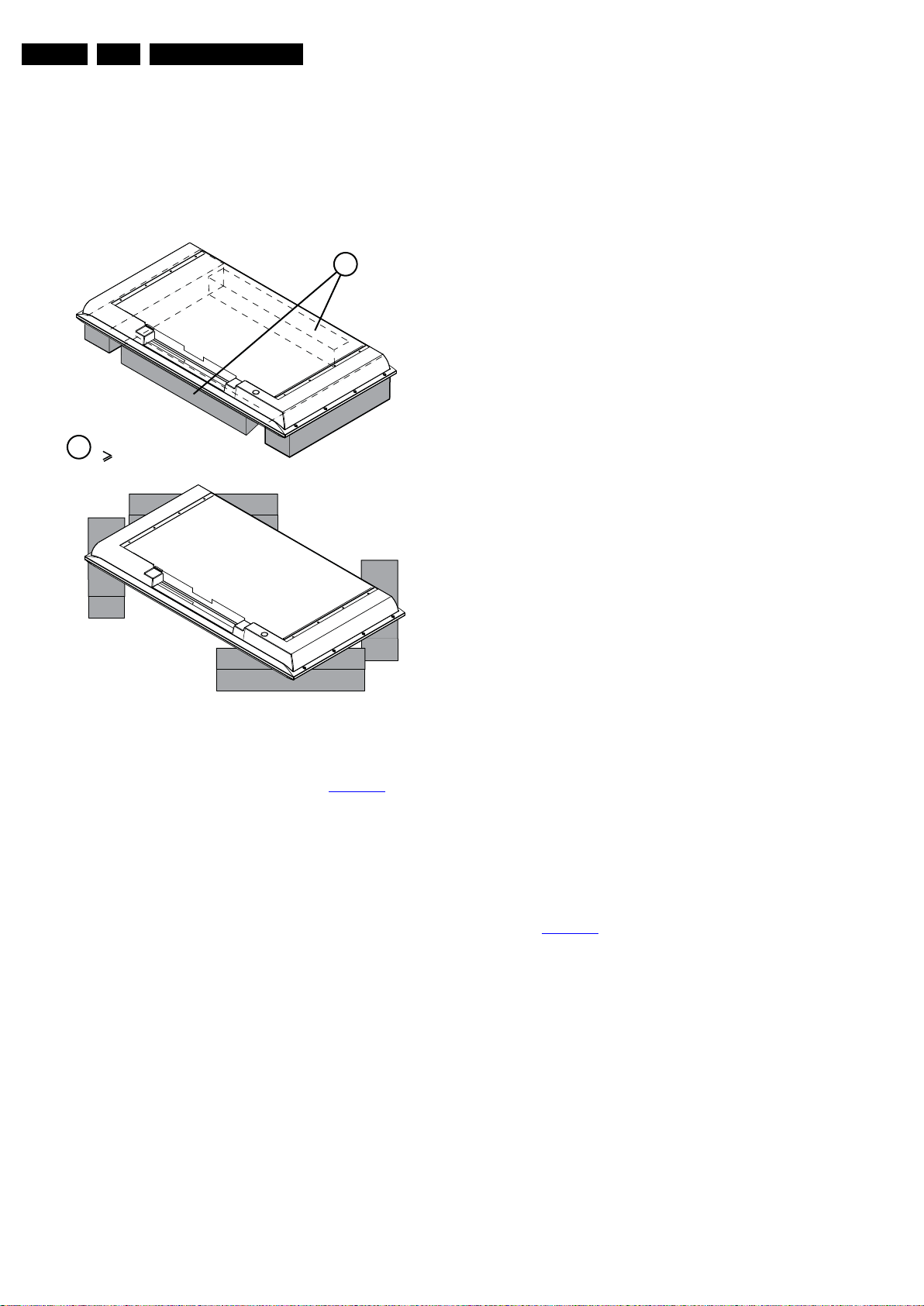
The foam bars (order code 3122 785 90580 for two pieces) can
be used for all types and sizes of Flat TVs. See Figure 4-3
details. Sets with a display of 42" and larger, require four foam
bars [1]. Ensure that the foam bars are always supporting the
cabinet and never only the display.
Caution: Failure to follow these guidelines can seriously
damage the display!
By laying the TV face down on the (ESD protective) foam bars,
a stable situation is created to perform measurements and
alignments. By placing a mirror under the TV, the screen can
be monitored.
Figure 4-3 Foam bars
4.3.5 Small Signal Board (SSB)
Caution: it is mandatory to remount all different screws at their
original position during re-assembly. Failure to do so may result
in damaging the SSB.
1. Remove the fixation screws that secure the shielding.
2. Unplug the LVDS connector.
Caution: be careful, as these are very fragile connectors!
3. Unplug all other connectors.
4. The SSB can now be taken out of the set.
for
4.3.6 Speakers
1. Release the speaker connector from the unit.
2. Remove the fixation screws (only for 26”).
3. Take the speakers out together with their casing.
When defective, replace the whole unit.
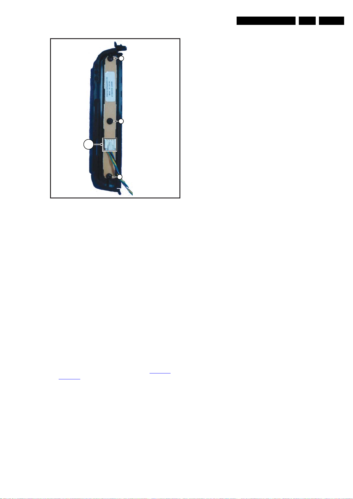
4.3.7 Keyboard Control Panel
Refer to Figure 4-4
1. Unplug the connector [1].
2. Remove the cover screws [2] and take out the whole unit.
When defective, replace the whole unit.
for details.
2010-Jun-18
Mechanical Instructions
18250_102_090210.eps
090611
1
2
2
2
EN 13TPS2.1L LA 4.
Figure 4-4 Keyboard Control Panel
4.3.8 IR Board
1. Remove screw and lift the IR Board from the front cover.
2. Unplug the connector.
When defective, replace the whole unit.
4.3.9 LCD Panel
1. Remove the PSU and SSB as described earlier.
2. Unplug all the connectors.
3. Remove the fixation screws from the clips that secure the
panel to the front.
4. The LCD panel can now be lifted from the front cabinet.
When defective, replace the whole unit.
4.4 Set Re-assembly
To re-assemble the whole set, execute all processes in reverse
order.
Notes:
• While re-assembling, make sure that all cables are placed
• Pay special attention not to damage the EMC foams on the
and connected in their original position. See Figure 4-1
Figure 4-2
SSB shields. Ensure that EMC foams are mounted
correctly.
.
and
2010-Jun-18
EN 14 TPS2.1L LA5.
18270_207_090603.eps
090611
Service Modes, Error Codes, and Fault Finding
5. Service Modes, Error Codes, and Fault Finding
Index of this chapter:
5.1
Service Modes
5.2 Service Tools
5.3 Error Codes
5.1 Service Modes
The Customer Service Mode (CSM) is used for communication
between the call center and the customer, while the Factory
Mode offers several features for the service technician.
This chassis also offers the option of using ComPair, a
hardware interface between a computer and the TV chassis. It
offers the abilities of structured troubleshooting, error code
reading, and software version read-out for all chassis.
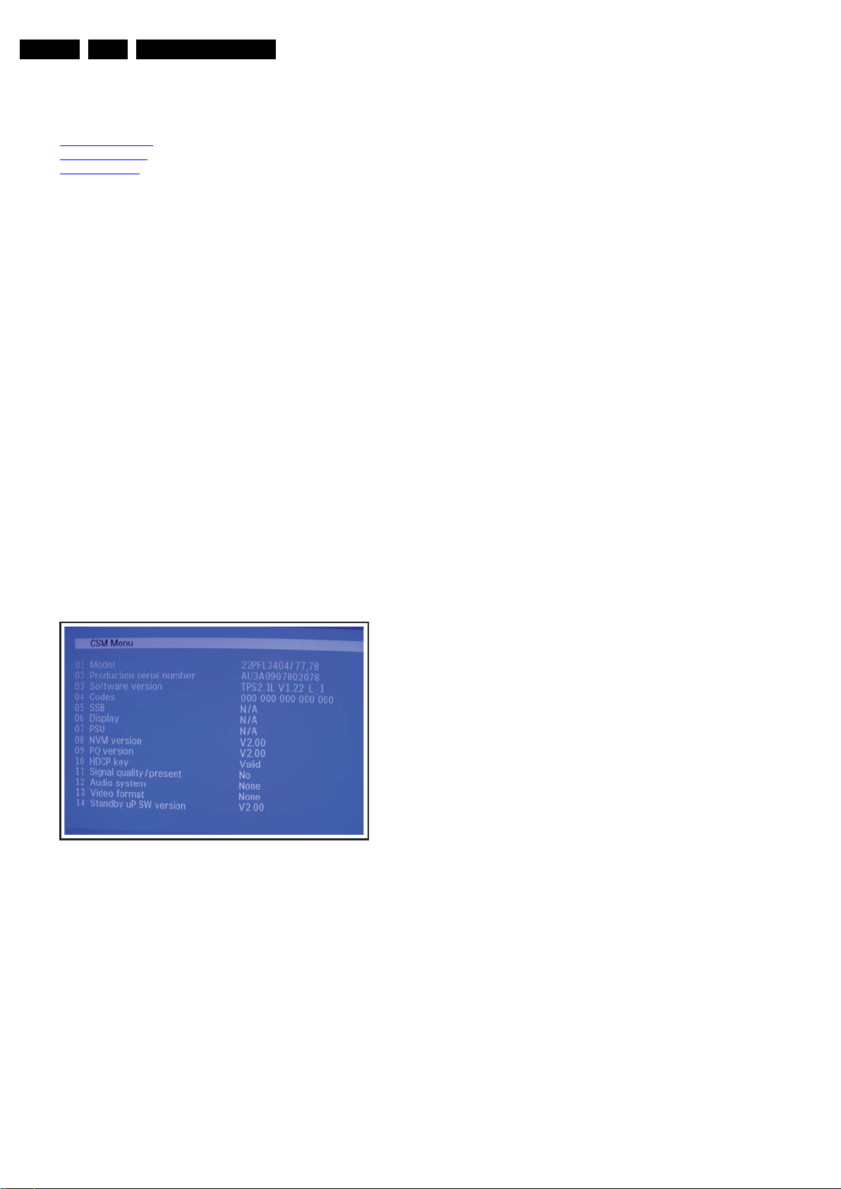
5.1.1 Customer Service Mode (CSM)
Purpose
The Customer Service Mode shows error codes and
information on the TV’s operation settings.The call center can
instruct the customer (by telephone) to enter CSM in order to
identify the status of the set.This helps the call center to
diagnose problems and failures in the TV set before making a
service call.
The CSM is a read-only mode; therefore, modifications are not
possible in this mode.
• Codes
Show the latest 5 error codes (layer 2)status:
000 = No problem, 011 = I
• SSB
Philips 12NC of SSB (small signal board)
• Display
Philips 12NC of display (LCD panel)
• PSU
Philips 12NC of PSU (Power Supply Unit)
• NVM version
Revision (4 letters)
• PQ Version
Revision (4 letter): if 1st version release, please
useV2.00...then V2.01....V2.02.....V2.03....etc
• HDCP key
HDCP status (Valid, Invalid)
• Signal quality/present
DTV shows (Digital percentage)
ATV shows (analog Yes/No)
• Audio system
Mono, Stereo, Dual
• Video format
PAL, SECAM, NTSC
• Standby μP SW version
Revision (4 letters)
How to Exit CSM
Press “MENU” on the RC-transmitter.
2
C bus error, 012 = tuner error
How to Activate CSM
Key in the code “123654” via the standard RC transmitter.
Note: Activation of the CSM is only possible if there is no (user)
menu on the screen!
Figure 5-1 CSM MENU
How to Navigate
By means of the “CURSOR-DOWN/UP” knob (or the scroll
wheel) on the RC-transmitter, can be navigated through the
menus.
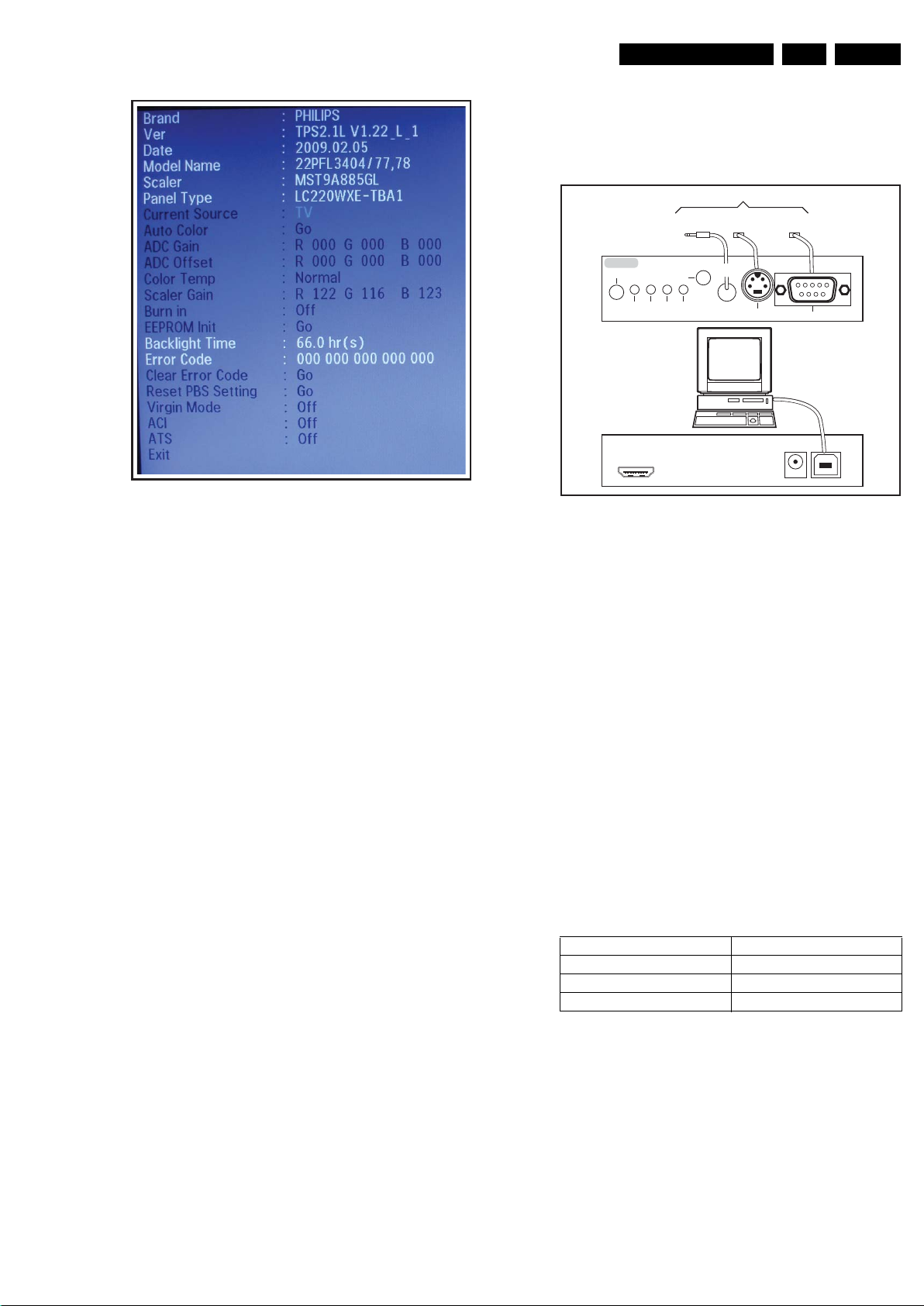
5.1.2 Factory mode
How to enter
To enter the factory mode, use the following method:
• Press the Menu button on the standard remote control.
• Press the following key sequence on the remote control
transmitter1999” directly followed by the “MENU” button.
Note: The factory mode can be entered by the following
method: (only for 22")
• Turn on the monitor, press the “MENU” key.
• Press the following key sequence on the remote control
transmitter: ”062596”, then press “INFO” key.
Caution: This functions are available for development and
service personal only, not for end customers.
After entering the factory mode, the following screen is visible
with panel information at the bottom line in the menu.
Contents of CSM
• Model. Philips model type(12characters max)
• Production serial number
Philips serial number(14characters max)
• Software version
Format:TPAA.AA V2.XX Y Z
TPAA.AA is the chassis name
V2.XX is the revision
Y is the display code (1 digit).
Z is the panel revision code (1 digit).
2010-Jun-18
Service Modes, Error Codes, and Fault Finding
18270_208_090603.eps
090611
10000_036_090121.eps
091118
TO
UART SERVICE
CONNECTOR
TO
UART SERVICE
CONNECTOR
TO
I2C SERVICE
CONNECTOR
TO TV
PC
HDMI
I
2
C only
Optional power
5V DC
ComPair II Developed by Philips Brugge
RC out
RC in
Optional
Switch
Power ModeLink/
Activity
I
2
C
ComPair II
Multi
function
RS232 /UART
EN 15TPS2.1L LA 5.
How to Navigate
when you press the up/down cursor keys you can move around
the items, with the “Right cursor” any item can be selected and
entered, with the “MENU” button on the remote control, the set
will switch on the normal user menu in the factory mode.
How to EXIT
Choose “exit”, then press “OK” button.
5.2 Service Tools
5.2.1 ComPair
Introduction
ComPair (Computer Aided Repair) is a Service tool for Philips
Consumer Electronics products. and offers the following:
1. ComPair helps to quickly get an understanding on how to
2. ComPair allows very detailed diagnostics and is therefore
3. ComPair speeds up the repair time since it can
4. ComPair features TV software up possibilities.
Specifications
ComPair consists of a Windows based fault finding program
and an interface box between PC and the (defective) product.
The ComPair II interface box is connected to the PC via an
USB cable. For the TV chassis, the ComPair interface box and
the TV communicate via a bi-directional cable via the service
connector(s).
The ComPair fault finding program is able to determine the
problem of the defective television, by a combination of
automatic diagnostics and an interactive question/answer
procedure.
Figure 5-2 Factory Mode Menu
repair the chassis in a short and effective way.
capable of accurately indicating problem areas. No
knowledge on I
2
C or UART commands is necessary,
because ComPair takes care of this.
automatically communicate with the chassis (when the uP
is working) and all repair information is directly available.
Figure 5-3 ComPair II interface connection
Caution: It is compulsory to connect the TV to the PC as
shown in the picture above (with the ComPair interface in
between), as the ComPair interface acts as a level shifter. If
one connects the TV directly to the PC (via UART), ICs will be
blown!
How to Order
ComPair II order codes:
• ComPair II interface: 3122 785 91020.
• Programming software can be downloaded from the Philips
Service portal.
• ComPair UART interface cable 3122 785 90004 and
adapter cable 3139 131 03791.
Note: When having problems, contact the local support desk.
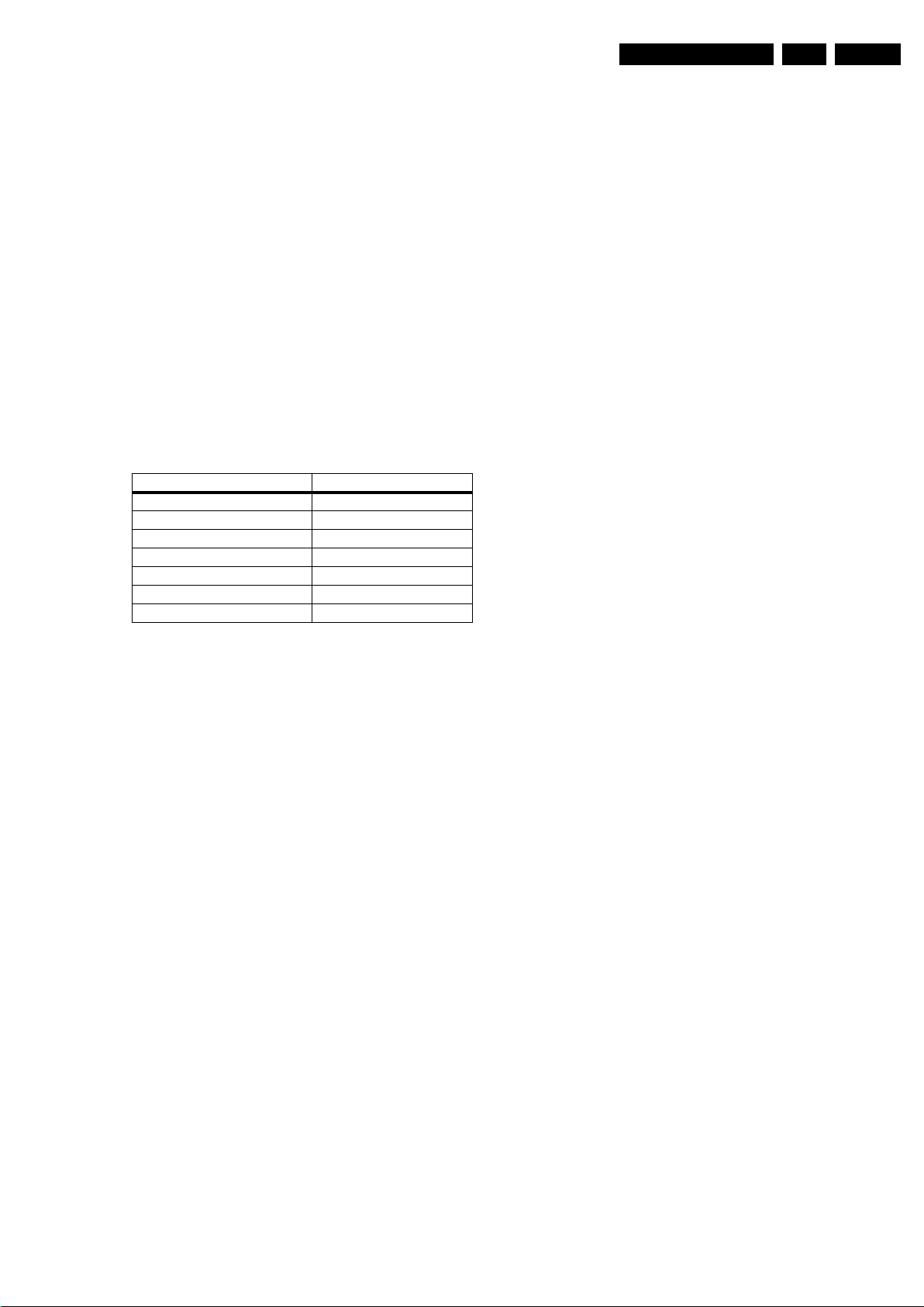
5.3 Error Codes
5.3.1 Error Buffer
Table 5-1 Error Code Overview
Error Code Description
000 No problem
011 I
012 Tuner error
2
C bus error
How to Connect
This is described in the chassis fault finding database in
ComPair.
2010-Jun-18

EN 16 TPS2.1L LA6.
6. Alignments
Alignments
Index of this chapter:
6.1
General Alignment Conditions
6.2 Hardware Alignments
6.3 Software Alignments
6.4 Reset of Repaired SSB
6.5 Serial Number Definition
Note: The Service Alignment Mode (SAM) is described in
chapter 5.
Menu navigation is done with the CURSOR UP, DOWN, LEFT
or RIGHT keys of the remote control transmitter.
Service Modes, Error Codes, and Fault Finding.
6.1 General Alignment Conditions
Perform all electrical adjustments under the following
conditions:
• Power supply voltage: 220 - 240 V
• Connect the set to the mains via an isolation transformer
with low internal resistance.
• Allow the set to warm up for approximately 15 minutes.
• Measure voltages and waveforms in relation to correct
ground (e.g. measure audio signals in relation to
AUDIO_GND).
Caution: It is not allowed to use heatsinks as ground.
• Test probe: Ri > 10 MΩ, Ci < 20 pF.
• Use an isolated trimmer/screwdriver to perform
alignments.
/ 50 ± 3 Hz.
AC
6.2 Hardware Alignments
Not applicable.
6.3 Software Alignments
With the software alignment in “Factory” mode, the tuner and
RGB settings can be aligned.
To store the data: use on the RC the “MENU” button to switch
to the main menu and then switch to “Stand-by” mode.
6.3.1 White Alignment
Before alignment, choose “MENU” -> “Picture” and set:
• “Brightness” to “50”.
• “Contrast” to “100”.
Then enter “Factory/SAM” mode to start the alignments.
When a color analyzer is available:
• Measure with a calibrated (phosphor- independent) color
analyzer (e.g Minolta CA-210) in the center of screen
Consequently, the measurement needs to be done in a
dark environment.
• Select a COLOR TEMPERATURE (e.g. COOL, NORMAL,
or WARM).
• Adjust the correct x,y coordinates (while holding one of the
White point registers R, G or B on “127”) by means of
decreasing the value of one or two other white points to the
correct x,y coordinates (see table “White D alignment
values xx”).
• Repeat this step for all color temperatures that need to be
aligned.
• When finished, press STANDBY on the RC to store the
aligned values to the NVM.
Table 6-1 White D alignment values 22"
Value Cool (11000 K) Normal (9000 K) Warm (6500 K)
x 0.278 ± 0.015 0.289 ± 0.015 0.314 ± 0.015
y 0.278 ± 0.015 0.291 ± 0.015 0.319 ± 0.015
Table 6-2 White D alignment values 26"
Value Cool (11000 K) Normal (9000 K) Warm (6500 K)
x 0.278 ± 0.004 0.289 ± 0.004 0.314 ± 0.004
y 0.278 ± 0.004 0.291 ± 0.004 0.319 ± 0.004
If no color analyzer is available, you can use the default
values. This is the next best solution. The default values are
average values coming from production (statistics).
• Select a COLOR TEMPERATURE (e.g. COOL, NORMAL,
or WARM).
• Set the RED, GREEN and BLUE default values according
to the values in the “Tint settings” table.
• When finished, press STANDBY on the RC, to store the
aligned values to the NVM.
Table 6-3 Tint settings 22"
Color Temp. R G B
Cool 115 111 124
Normal 122 116 123
Warm 119 108 106
Table 6-4 Tint settings 26"
Color Temp. R G B
Cool 123 110 122
Normal 119 104 112
Warm 114 95 90
6.3.2 Input Adjustment
1. Apply a color bar pattern (see below) to the input that must
be aligned, and set “Brightness” and “Contrast” to 50%.
2. Enter “Factory/SAM” mode to start the alignments.
3. Select the source to align: TV/CVI1/CVI2/VGA/HDMI1/AV
IN/AV side.
4. Activate the “Auto Color” function for auto ADC Offset and
ADC Gain alignment. Check if scales are distinguishable.
5. Perform this alignment for all sources.
2010-Jun-18
18290_200_090330.eps
Figure 6-1 Color bar pattern (TVBAR 100)
090416
6.4 Reset of Repaired SSB
A very important issue towards a repaired SSB from a service
repair workshop, implies the reset of the NVM on the SSB.
A repaired SSB in service should get the service Set Type
“00PF0000000000” and Production Code “00000000000000”.
Also the virgin bit is to be set. To set all this, you can use the
ComPair tool.
Due to the compensation needed for the backlight of these TV
sets, the item “Backlight time” value, stored in NVM, must be
reset in a spare SSB with the original value of the TV set.
“Backlight time” value can be found in the SAM (062596 + info
button).
In case of a display replacement, reset the “Backlight time” to
“0”, or to the operation hours of the replacement display.
6.5 Serial Number Definition
Table 6-5 BOM Code
Panel Supplier Code
AU 1
CPT 2
LPL(LG) 3
QDI 4
CMO 5
HSD 6
SVA 7
Alignments
EN 17TPS2.1L LA 6.
2010-Jun-18
EN 18 TPS2.1L LA7.
18270_209_090603.eps
090611
VIDEO
DECODER
AUDIO
DECODER
SCALER
MST9A885GL
U4201
PC
SIDE-AV
COMPONE NT 1
HDMI
MCU
WT6703F
U4101
FLASH
S25FL032
U4403
Y Pb Pr 1
CVBS
R G B
TUNER
TUNER_CVBS
HDCP-CODE
M24C32
U4203
LR
Com ponent Audio
JACK
PC Au dio
SIDE-AV
Side-AV Audio
TUN ER_S IF
LVDS
Panel
CVBS OUT
U1201
DRV601
Lineout
AUD_OUT
CN 1205
U6101
DRV601
AUD_OUT
U6102
Am plif ier
SPEAKER
I2C _S CL I2C _S DA
U4401
DDR
U1503
SCL_HD SDA_H D
EDID
U150 1
TMD S
TMD S
ISP_SCL ISP_SDA
COMPONE NT 2
Y Pb Pr 2
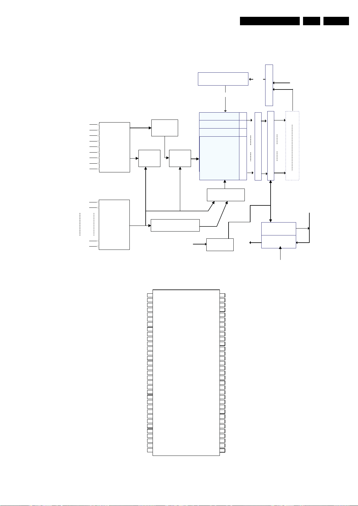
7. Circuit Descriptions
Circuit Descriptions
Index of this chapter:
7.1
Introduction
7.2 MST9A885GL
Notes:
•Only new circuits (circuits that are not published recently)
are described.
• Figures can deviate slightly from the actual situation, due
to different set executions.
• For a good understanding of the following circuit
descriptions, please use the wiring, block (chapter 6) and
circuit diagrams (chapter 7). Where necessary, you will find
a separate drawing for clarification.
7.1 Introduction
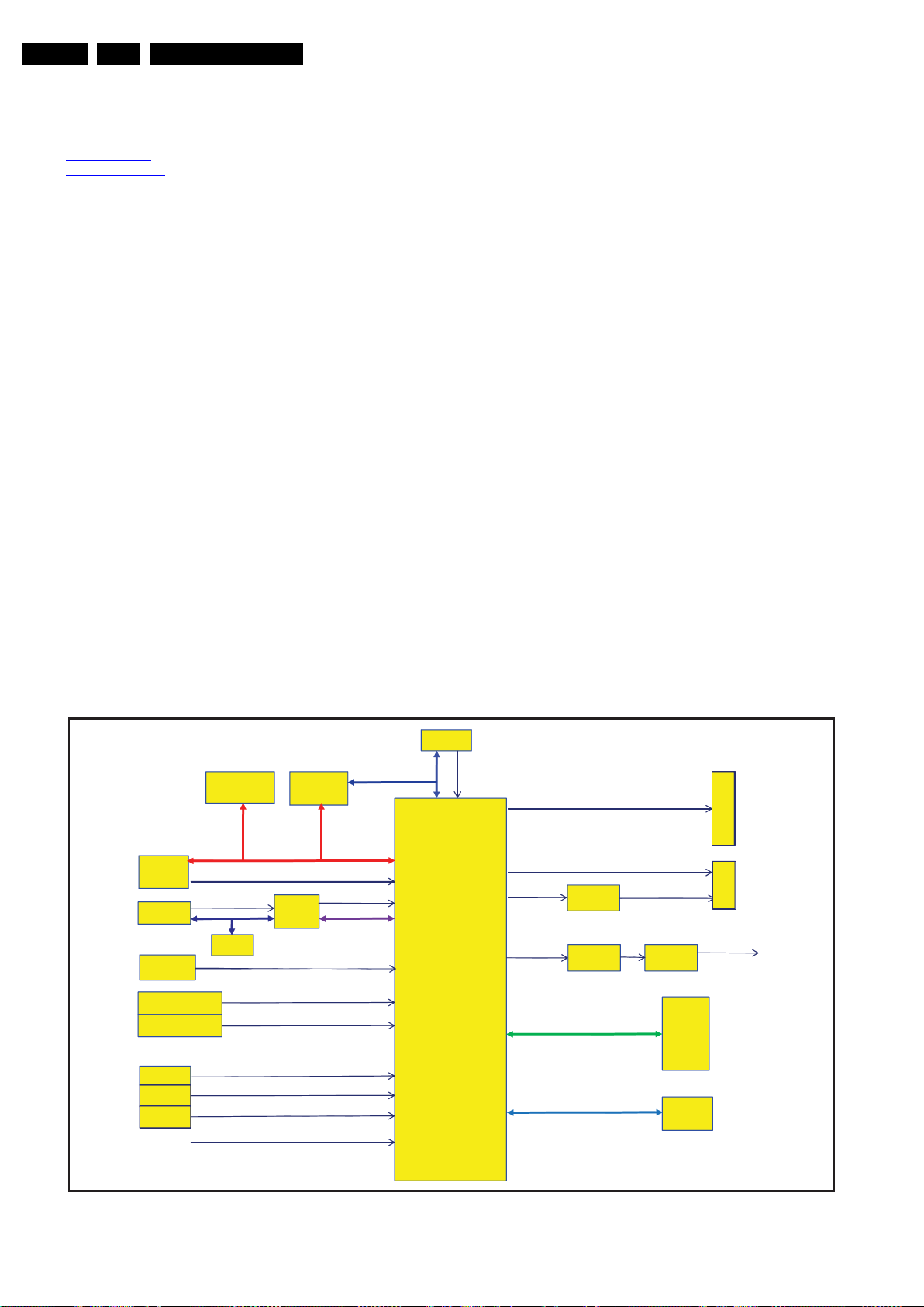
The 2K9 LCD-TV AL3 platform supports RF TV; PC VGA input
and DVI digital input via HDMI connector, up to 1366 × 768 at
60 Hz timing mode for WXGA mode. Besides that it supports
CVBS and also YPbPr (CVI) signal. HDMI signal input from
SDTV to HDTV format (480i/p, 576i/p, 720p, 1080i/p).
26PFL3404 is the 5th generation of Fighter series Flat Panel
Display TV with lead free policy. The TV features with good
stability. The power button and display control buttons (tact
switch type) are on the right side of the TV; IR sensor is on the
front of the TV. AC inlet, RF, YPbPr, SCART1, SCART 2,
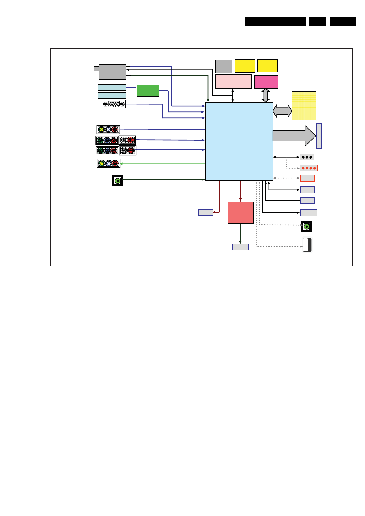
7.1.1 Block Diagram
HDMI1, SPDIF are on the rear side of the TV; Side HDMI and
Side AV are on the left side of the TV. And it is modularized as
a display unit with embedded EU AC power (220VAC ±10%)
supplies inside TV main body.
This platform uses the fully integrated scaler chip by M-STAR
MST9A885XX which has embedded ADC for CVI/VGA input;
decoder for HDMI/DVI digital data stream; audio decoder;
close caption (CC) decoder; micro controller; OSD engine;
LVDS transmitter for up/down scaling.
It designs with IPS/MVA panel, LVDS interface. For TV signal
MST9A885GL DSP supports baseband CVBS by can tuner for
multi-TV standards by region NTSC/PAL/SECAM, SIF
demodulation for NICAM/FM stereo and SAP.
The MST9A885XX is embeds the 3D de-interlace to generate
very smooth picture quality for motion video. 2D/3D comb filter
also renders rich details for still image. The special color
processing engine provides good picture quality for noise
reduction, enhancement of edge sharpness and color
performance. It also apply some dynamic feature for contrast,
backlight control to increase contrast ratio (CR).
To enrich the features of analog TV (ATV), MST9A885GL has
an built-in HDMI receiver to support digital signal with HDCP
function, integrated with high bandwidth VGA ADC, high
resolution Video/Audio ADC, 90 dB Audio DAC and 10-bit
Video DAC. It will provide a high performance for multi-function
LCD TV/Monitor.
Multi-input source of video signal will be delivered to
MST9A885XX for further processing. MUX selects audio input
source and digitalizes/processes audio signal, then
transformed by audio DAC and output to audio amplifier
TPA3124. The MST9A885XX supports LVDS interface to
panel for displaying image:
• RF input: MM tuner for PAL (M/N)
• HDMI/DVI input: 1 (rear) +1 (side)
• CVI with audio input: double YPbPr component video with
R/L audio
• AV input: CVBS with R/L audio, 1 (rear) +1 (side)
• PC input: VGA (Dsub) + AUDIO IN (3.5 mm mini-jack)
2010-Jun-18
Figure 7-1 Block Diagram 22"
Circuit Descriptions
18270_205_090529.eps
090611
ren
uTFR
o
iduA
C
P
LG588A9TS
M
SBVC
0RUA ,0LUA ,rP,,bP,,
Y
3RUA ,3LUA ,1SBVC
FI
S
RDD
zHM002
61xM8
hsalF IPS
M2/MOR
20C42
DIDE BUSD
23C42
MARVN
C2
I
3213APT
SDVL/LTT
lenaP DCL
IPS
riaP moC
1TRAU
gninol
C
)1-VTi(
)P5(
F/I oediV
)2-VTi
(
)P2(x2
rekaepS R-L
1RUA ,1LUA ,rP,,bP
,,Y
nI VA
tuo-eniL
/PH moorhtaB
rekaepS
)2-VTi(
BUS-D
1B
,1G,1R
20C4
2
DIDE IVD
Note: Reserved for iTV only
3076TW
UCM YBDTS
edis IMDH
WS 1 ot
2
IMDH
)P3(
2RUA ,2LUA
tuO VA
0
TUOENIL / 1TUOSBVC
P11
)P3(
)P7
(
draoB RI
draoB yeK
lortnoc SPIL
tuo
FIDP
S
)
devreseR(
BSU
ediS
)devreseR(
1-tnenopmo
C
2-tnenopmo
C
EN 19TPS2.1L LA 7.
Figure 7-2 Block Diagram 26"
2010-Jun-18
EN 20 TPS2.1L LA7.
18270_210_090603.eps
090611
CVI1
CVI2
AV I N
AV OUT
AV I N
Tuner
VGA
HDMI
Scaler
MCU
DDR
Flash
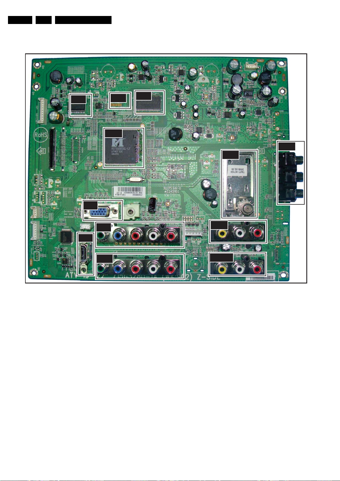
7.1.2 SSB Cell Layout
Circuit Descriptions
Figure 7-3 SSB top view 22"
2010-Jun-18

Circuit Descriptions
EN 21TPS2.1L LA 7.
7.2 MST9A885GL
In this chassis, the MST9A885GL is a high performance and
fully integrated IC with resolutions up to SXGA (1280 × 1024)
/ WXGA+ (1440 × 900). It is configured with an integrated
triple-ADC/PLL, an integrated DVI/HDCP/HDMI receiver, a
multi-standard TV video and audio decoder, a video
de-interlacer, a scaling engine, the MStar ACE-3 color engine,
an on-screen display controller, an 8-bit MCU and a built-in
output panel interface. By use of external frame buffer, 3-D
video decoding and processing are fulfilled for high-quality TV
applications. To further reduce system costs, the
MST9A885GL also integrates intelligent power management
control capability for green-mode requirements and spreadspectrum support for EMI management.
Host CPU
• Embedded 8032 micro controller
• Configurable PWMs and GPIOs
• Low speed ADC inputs for system control.
• SPI bus for external flash
• Supports external MCU option controlled through 4-wire
double-data-rate direct MCU bus
• Build-in CPI analyzer.
Transport De-multiplexer
• Integrated DVI/HDCP/HDMI receiver
• Integrated multi-standard TV video and audio decoder
• Integrated 8 bit MCU
• Integrated Output panel interface
• Integrated Video de-interlacer and Scaling.
NTSC/PAL/SECAM Video Decoder
• Supports NTSC-M, NTSC-J, NTSC-4.43, PAL (B, D, G, I,
K, M, N, Nc), and SECAM
• Automatic TV standard detection
• Motion adaptive 3-D comb filter for NTSC/PAL
• 8 configurable CVBS & Y/C S-video inputs
• Supports Teletext level-1.5, WSS, VPS, Closed-caption,
and V-chip
• CVBS video output.
• With 6/8 bits options
• Reduced swing for LVDS for low EMI
• Supports flexible spread spectrum frequency with
360 Hz ~ 11.8 MHz and up to 25% modulation.
CVBS In
• On chip 54 MHz 10 bit video ADC
• Support PAL (B, G, D, H, M, N, I, Nc), NTSC, NTSC-4.43,
SECAM
• NTSC/PAL support 3D motion adaptive comb filter and
SECAM support 2D comb filter
• Motion adaptive 3D noise reduction (NR) built in
• VBI data slicer for CC/TT decoding
• Supporting 4 CVBS, 2 S-video.
Analog RGB Compliant Input Ports
• Three analog ports support up to WXGA
• Supports RGB/YPbPr/YCbCr
• Supports Composite Sync and SOG (Sync-on-Green)
separator
• Automatic color calibration.
DVI/HDCP/HDMI Compliant Input Port
• Supports TMDS clock up to 225 MHz @ 1 080p, 60 Hz with
12 bit deep-color resolution
• Single link on-chip DVI 1.0 compliant receiver
• High-bandwidth Digital Content Protection (HDCP) 1.1
compliant receiver
• High Definition Multimedia Interface (HDMI) 1.3 compliant
receiver with CEC support
• Long-cable tolerant robust receiving
• Support HD up to WXGA.
Multi-Standard TV Sound Decoder
• Supports BTSC/NICAM/A2/EIA-J demodulation and
decoding
• FM stereo & SAP demodulation
• L/Rx4, mono, and SIF audio inputs
• L/Rx3 loudspeaker and line outputs
• Supports sub-woofer output
• Built-in audio output DACs.
Digital Audio Interface
• I2S digital audio input & output
• S/PDIF digital audio input & output
• HDMI audio channel processing capability
• Programmable delay for audio/video synchronization.
On-Screen OSD Controller
• 16/256 color palette
• 256/512 1-bit/pixel font
• 128/256 4-bit/pixel font
• Supports texture function
• Supports 4K attribute/code
• Horizontal and vertical stretch of OSD menus
• Pattern generator for production test
• Supports OSD MUX and alpha blending capability
• Supports blinking and scrolling for closed caption
applications.
LVDS Panel Interface
• Supports 8-bit dual link LVDS up to WXGA
• Supports 2 data output formats: Thine & TI data mappings
• Compatible with TIA/EIA
2010-Jun-18
EN 22 TPS2.1L LA8.
18250_300_090210.eps
090318
SIF
VIDEO
AUDIO
RF AGC
+5V
SCL
SDA
AS
LOW BAND
HIGH BAND
MID BAND
RF AGC
PLL
MIXER & OSC & PLL
UHF
OSC
VHF
OSC
IF
VT
DC/DC
VIF PLL
DEMODULATOR
SOUND
DEMODULATOR
SAW
SAW
V
ANT IN. (RF IN)
IF
IF
S
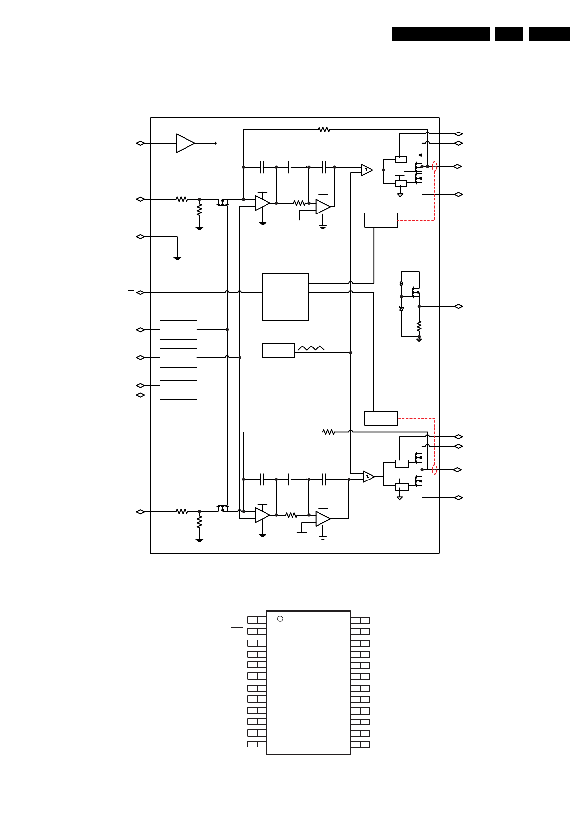
8. IC Data Sheets
IC Data Sheets
This section shows the internal block diagrams and pin
configurations of ICs that are drawn as “black boxes” in the
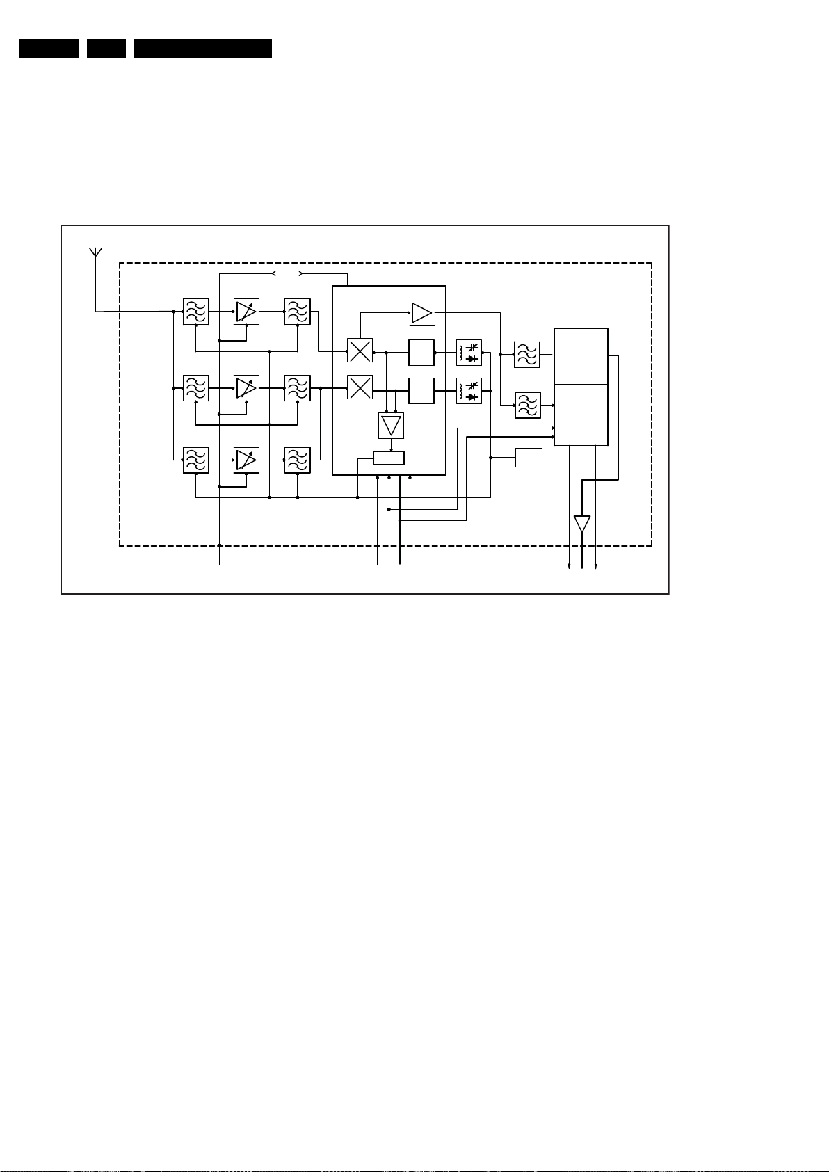
8.1 Diagram B04, TAFT-x710x (IC TU1101)
electrical diagrams (with the exception of “memory” and “logic”
ICs).
Figure 8-1 Internal Block Diagram
2010-Jun-18
8.2 Diagram B07, MST9A885GL-LF (IC U4201)
Pin 1
13
14
17
18
21
23
25
27
28
30
32
34
36
39
41
43
15
16
19
20
22
24
26
29
31
33
35
37
38
40
42
44
45
46
47
48
50
51
52
49
REXT
HSYNC1
VSYNC1
VCLAMP
REFP
REFM
BIN1P
RI N1 P
BIN0P
GIN0P
RI N0 P
AVDD_33
HSYNC0
VSYNC2
SOGI N1
GIN1P
VCOM2
VCOM3
SOGI N0
GND
VSYNC0
BIN2P
SOGI N2
GIN2P
RI N2 P
C1
Y1
C0
Y0
CVB S3
CVB S2
CVB S1
VCOM1
AVDD_33
CVBSOUT1
CVBSOUT0
GND
GPIOL[0]
GPIOL[1]
GPIOL[4]
XOUT
AVDD_MPLL
GND_ VI FPLL
VR27
VR12
1
2
3
4
5
7
9
11
6
8
10
12
53
54
55
56
57
59
61
63
58
60
62
64
GND_RXS
SIFP
SIFM
VI FM
VI FP
AVDD_RXV
TAFC
AVD D_TAG C
GND_ TAG C
TAGC
AVDD_AU
77
78
81
82
85
87
899192
94
96
98
100
103
105
107
79
80
83
84
86
88
90
93
959799
101
102
104
106
108
109
110
111
112
114
115
116
113
AUVAG
AVDD_AU
LINE_IN_0L
LINE_IN_0R
LINE_IN_1L
LINE_IN_1R
AUCOM
LINE_IN_3L
LINE_IN_MONO
LINE_OUT_3R
LINE_OUT_2R
LINE_OUT_1R
LINE_OUT_0R
GPIOD[0]
LINE_IN_2L
LINE_IN_2R
LINE_IN_3R
LINE_OUT_3L
LINE_OUT_2L
LINE_OUT_1L
LINE_OUT_0L
GPIOD[1]
GPIOD[2]
GND
VDDC
WRZ
RDZ
ALE
BADR[1]
BADR[0]
RASZ
VDDC
GND
AVDD_MI
CASZ
WEZ
MADR[11]
MADR[10]
656667
68
69
71
73
75
70
72
74
76
117
118
119
120
121
123
125
127
122
124
126
128
MADR[9]
MADR[8]
MADR[7]
MADR[6]
MADR[5]
MADR[4]
MADR[1]
MADR[3]
MADR[2]
MADR[0]
180
179
176
175
172
170
168
166
165
163
161
159
157
154
152
150
178
177
174
173
171
169
167
164
162
160
158
156
155
153
151
149
148
147
146
145
143
142
141
144
192
191
190
189
188
186
184
182
187
185
183
181
140
139
138
137
136
134
132
130
135
133
131
129
244
243
240
239
236
234
232
230
229
227
225
223
221
218
216
214
242
241
238
237
235
233
231
228
226
224
222
220
219
217
215
213
212
211
210
209
207
206
205
208
DDCD_SCL
DDCD_SDA
HPLUG
RX2P
RX2N
GND
RX0P
RX0N
AVDD_33
256
255
254
253
252
250
248
246
251
249
247
245
204
203
202
201
200
198
196
194
199
197
195
193
AUVRP
AVDD_ RXS
GND
GND
DI[7]
DI[6]
DI[5]
DI[4]
VDDP
DI[3]
DI[2]
DI[1]
DI[0]
VDDP
PWM2
PWM3
RXCKN
RXCKP
RX1N
VDDC
ICLK
GPIOT[0]
AUVRM
GND
CVB S0
VCOM0
AVDD_MI
PWM 0
SAR 2
SAR 0
GND
SPI_SCZ
SPI_SCK
GND
SAR 3
SAR 1
VDDC
SPI_SDO
SPI_SDI
USB20_DM
AVDD_USB
USB20_REXT
MVREF
MCLKE
MCLK
MCLKZ
DQM1
DQS1
MDATA[ 15]
MDATA[ 11]
MDATA[ 10]
AVDD_MI
MDATA[ 3]
MDATA[ 2]
GND
MDATA[ 1]
MDATA[ 0]
AVDD_MI
DQS0
DQM0
INT
DDCA_SCL
DDCA_SDA
DDCR_SCL
DDCR_SDA
PWM 1
GPIO R [ 0]
GPIOD[3]
GPIOD[5]
GPIOD[7]
GPIOD[4]
GPIOD[6]
VDDP
AVDD_MIPLL
GND _RX V
GND
USB20_DP
VDDP
GND
IRIN
VDDP
USB_DM
USB_VBUS
USB_DP
USB_CID
GPIOB[0]
GPIOB[1]
RX1P
GND
XIN
MDATA[ 9]
MDATA[ 8]
AVDD_MI
MDATA[ 7]
MDATA[ 6]
MDATA[ 5]
MDATA[ 4]
MDATA[ 14]
MDATA[ 13]
MDATA[ 12]
AVDD_MI
GPIOL[2]
GPIOL[3]
AD[0]
AD[1]
AD[2]
AD[3]
GND
VDDP
LVB0M
LVB0P
LVB1M
LVB1P
LVB2M
LVB2P
LVBCKM
LVBCKP
LVB3M
LVB3P
AVDD_MI
GND
VDDP
LVA0M
LVA0P
LVA1M
LVA1P
LVA2M
LVA2P
LVACKM
LVACKP
LVA3M
LVA3P
VDDC
GND
HWRESET
GPIOE[2]
GPIOE[0]
GPIOE[1]
GPIOE[3]
NC
NC
NC
NC
MST9A885
GL
18250_301_090210.eps
090210
Pin Configuration
IC Data Sheets
EN 23TPS2.1L LA 8.
XXXXXXXX
XXXXX
Figure 8-2 Pin Configuration
2010-Jun-18

EN 24 TPS2.1L LA8.
18250_302_090210.eps
090318
Pin Configuration
Block Diagram
Turbo 8051 MCU
8K bytes code flash
Internal 256
bytes SRAM
Eternal 128
bytes SRAM
32K Oscillator
RTC
RC Oscillator
Reset Processor
Clock Processor
Clock off & Wake Up
Watchdog timer
Interrupt Processor
8051 UART,
Timer0, Timer1
DDC
Slave IIC
HV DPMS Detector
CEC
IR Detector
PWM
4 IRQ Processor
GPIO Processor
Key Pad ADC
6703F-SG240WT
6703F-OG240WT
32K0SCO
32KOSCI
VSS
NRST
PWM1/GPIOC
PWM0/GPIOC0
RXD/IRQ3/GPIOB7
(CEC)/TXT/IRQ2/GPIOB6
HIN/GPIOB5
VIN/GPIOB4
(CEC)/IRQ1/P1.3/GPIOB3
IRQ0/P1.2/GPIOB2
VDD_RTC
VDD
GPIOA0/AD0
GPIOA1/AD1
GPIOA2/AD2
GPIOA3/AD3/IR
GPIOA4/P1.0
GPIOA5/P1.1
GPIOA6/DSCL
GPIOA7/DSDA
GPIOB0/SCL
GPIOB1/SDA/CEC
1
6
4
5
7
9
8
10
3
2
11
12
13
14
15
16
17
18
19
20
21
22
23
24
IC Data Sheets
8.3 Diagram B08, WT6703F-SG240WT (IC U4101)
2010-Jun-18
Figure 8-3 Internal Block Diagram and Pin Configuration
8.4 Diagram B09, HY5DU281622FTP-5-C (IC U4401)
Mode
Register
Command
Decoder
CLK
/CLK
CKE
/CS
/RAS
/CAS
/WE
LDM
UDM
Bank
Control
Mode
Register
Row
Decoder
2M×16 BANK 0
2M×16 BANK 1
2M×16 BANK 2
2M×16 BANK 3
Memory
Cell
Array
Sense AMP
Column
Decoder
Address
Buffer
A0
A1
A
max
BA0
BA1
Column Address
Decoder
16
Output Buffer
DQ0
DQ15
Input Buffer
DS
32
2-bit Prefetch Unit
Write Data Register
2-bit Prefetch Unit
16
32
Data Strobe
Transmitter
Data Strobe
Receiver
LDQS,
UDQS
LDQS,
UDQS
DLL
Block
CLK,
/CLK
CLK_DLL
Mode
Register
Pin Configuration
1
2
3
4
5
6
7
8
9
10
11
12
13
14
15
16
17
18
19
20
21
22
23
24
25
26
27
28
29
30
31
32
33
66
65
64
63
62
61
60
59
58
57
56
55
54
53
52
51
50
49
48
47
46
45
44
43
42
41
40
39
38
37
36
35
34
400mil x 875mil
66pin TSOP-I I
0.65mm pin pitch
V
DD
DQ0
V
DDQ
DQ1
DQ2
V
SSQ
DQ3
DQ4
V
DDQ
DQ5
DQ6
V
SSQ
DQ7
NC
V
DDQ
LDQS
NC
V
DD
NC
LDM
/WE
/CAS
/RAS
/CS
NC
BA0
BA1
A10/AP
A0
A1
A2
A3
V
DD
V
SS
DQ15
V
SSQ
DQ14
DQ13
V
DDQ
DQ12
DQ11
V
SSQ
DQ10
DQ9
V
DDQ
DQ8
NC
V
SSQ
UDQS
NC
VREF
V
SS
UDM
/CK
CK
CKE
NC
NC
A11
A9
A8
A7
A6
A5
A4
V
SS
18250_303_090210.eps
090318
Block Diagram
IC Data Sheets
EN 25TPS2.1L LA 8.
Figure 8-4 Internal Block Diagram and Pin Configuration
2010-Jun-18

EN 26 TPS2.1L LA8.
Block Diagram
Address
Generator
Memory Array
Page Buffer
Y-Decoder
X-Decoder
Data
Register
SRAM
Buff
er
SI/SIO0
SCLK
Clock Generator
State
Machine
Mode
Logic
Sense
Amplifier
HV
Generato
r
Output
Buffer
SO/SIO1
CS#,
WP#/ACC,
HOLD#
1
2
3
4
CS#
SO/SIO1
WP#/ACC
GND
VCC
HOLD#
SCLK
SI/SIO0
8
7
6
5
Pin Configuration
18270_308_090603.eps
090603
IC Data Sheets
8.5 Diagram B09, MX25L1605DM2I-12G for 22" (IC U4402)
2010-Jun-18
Figure 8-5 Internal Block Diagram and Pin Configuration
8.6 Diagram B14, TPA312xD2PWPR (IC U6102)
LS
HS
LS
HS
OSC/RAMP
MUTE
CONTROL
BYPASS
AV
CONTROL
CONTROL
BIAS
THERMAL
SC
DETECT
SC
DETECT
AVD D
AVCC
LIN
RIN
MUTE
BYPASS
GAIN1
GAIN0
SD
BSL
PVCCL
LOUT
PGNDL
VCLAMP
BSR
PVCCR
ROUT
PGNDR
VCLAMP
VCLAMP
AVDD
AVD D
AVD D/2
AVD D
AVD D
AVD D/2
REGULATOR
AGND
+
-
+
-
1
2
3
4
5
6
7
8
9
10
11
12
24
23
22
21
20
19
18
17
16
15
14
13
PVCCL
SD
PVCCL
MUTE
LIN
RIN
BYPASS
AGND
AGND
PVCCR
VCLAMP
PVCCR
PGNDL
PGNDL
LOUT
BSL
AVCC
AVCC
GAIN0
GAIN1
BSR
ROUT
PGNDR
PGNDR
PWP (TSSOP) PACKAGE
(TOP VIEW)
Pin Configuration
Block Diagram
18250_305_090210.eps
090318
IC Data Sheets
EN 27TPS2.1L LA 8.
Figure 8-6 Internal Block Diagram and Pin Configuration
2010-Jun-18

EN 28 TPS2.1L LA8.
_
+
_
+
_
+
_
+
_
+
REF
REF
Load Comparator
Skip Comparator
Current Limit Comparator
P-Channel
Power MOSFET
Driver
Shoot-Through
Logic
Control
Logic
Soft Start
1 MHz
Oscillator
Comparator
S
R
N-Channel
Power MOSFET
Comparator High
Comparator Low
Comparator Low 2
V
(COMP)
Sawtooth
Generator
V
I
Undervoltage
Lockout
Bias Supply
_
+
Comparator High
Comparator Low
Comparator Low 2
Compensation
V
REF
= 0.5 V
R2
See Note
R1
V
I
EN
SW
D
NG
BF
Gm
Block Diagram
For the adjustable version (TPS62200) the internal feedback divider is disabled and the FB pin is
directly connected to the internal GM amplifier.
18270_306_090529.eps
090611
IC Data Sheets
8.7 Diagram B16, TPS62203DBVRG4 (IC U7101)
Figure 8-7 Internal Block Diagram
2010-Jun-18
9. Block Diagrams
Key Pad
4 Pin
18270_404_090602.eps
090611
CN853
CN851
CN833
CN831
PSU
11 Pin
111
CN902
1
5
CN0201
IR BOARD
5 Pin
AC IN
SSB
CN7201
1
10
10 Pin
CN7502
30 Pin
1
30
CN7301 CN7306
4 Pin
1
4
7 Pin
1
7
MST9A885GL-LF
U4201
FFC Cable
Panel
CN6101
RL
4 Pin
SERV.C
Speaker L/R
Wiring Diagram 22"
Block Diagrams
EN 29TPS2.1L LA 9.
2010-Jun-18
Wiring Diagram 26"
DRAOBNIAM
LENAP
POWER SUPPLY
308
N
C
209NC
tekcosCA
109NC
102
7NC
V21+
01
JD
A_TH
GIRB
11
FFO_n
o_r
etrev
nI
21
V21+9
DNG
8
DNG
7
DNG
6
V42+5
V42+
4
YBDNATS3
YBTSV5+2
YB
T
SV5
+1
3057NC
DNG
13
CCV_LENAP03
DNG91
DNG81
+1
EXR
71
-1EXR61
+0EXR51
-0
EXR41
+COXR11
-COX
R01
DNG9
DNG8
+2EXR12
-2
EXR02
+3OXR
31
-3OX
R21
+3EXR
52
-3
EX
R42
+
CEXR
3
2
-CEX
R22
CCV_LENAP92
CCV_LENAP82
DNG23
HGIH_
LE
NA
P72
)CN(RO62
+2OXR
7
-2OXR6
+1OXR
5
-1OXR
4
+
0OX
R
3
-0OXR2
DNG1
1037NC
D
NG4
2YEK
3
1
YEK2
FFO_NO-EWP1
KEY BOARD
6
0
37NC
IR BOARD
YBTSV5
+
3
NO_1DEL2
F
FO_
NO_RWP
1
ROSNESTHIG
L
7
DNG6
3V3_RI_CR5
YBTS2DEL4
YBTS_V5
+
4
G_DE
L
5
R_
DE
L
3
6CR
2
DNG
1
100NC
FFO_NO_W
P
4
1YEK
3
2
Y
E
K
2
DN
G
1
RREKAEPLS REKAEPS
1016NC
V5+
3
1
2
1
V
5+
1
1
B/S
0
1
V429
V428
DNG7
DNG6
DNG5
V214
V213
MID2
AN
E1
610NC
208NC
18270_402_090529.eps
090611
Block Diagrams
EN 30TPS2.1L LA 9.
2010-Jun-18
 Loading...