

Page 1

Colour Television Chassis
TPS1.2A
LA
I_17620_000.eps
260308
Contents Page Contents Page
1. Technical Specifications, Connections, and Chassis
Overview 2
2. Safety Instructions, Warnings, and Notes 5
3. Directions for Use 6
4. Mechanical Instructions 7
5. Service Modes, Error Codes, and Fault Finding 10
6. Block Diagrams, Test Point Overview, and
Waveforms
Wiring Diagram 13
Block Diagram Scaler Board 14
7. Circuit Diagrams and PWB Layouts Diagram PWB
Scaler Board: DC-DC Power (SB01) 15 33-34
Scaler Board: PS & Inverter I/F
Scaler Board: Tuner (SB03) 17 33-34
Scaler Board: Video Input 1 (SB04) 18 33-34
Scaler Board: Video Input 2 (Side AV) (SB05) 19 33-34
Scaler Board: D-Sub Input (SB06) 20 33-34
Scaler Board: HDMI Input 1
Scaler Board: HDMI Input 2 (n.c.) (SB08) 22 33-34
WT6702F (Standby MCU)
Scaler Board: Scaler MST98980CLD (SB09) 24 33-34
Scaler Board: Flash ROM & Memory (SB10) 25 33-34
Scaler Board: KEY, IR BD & Compair I/F
Scaler Board: ITV I/F
Scaler Board: Panel I/F
Scaler Board: Audio I/F
Scaler Board: Audio Amplifier (SB15) 30 33-34
Scaler Board: Audio Out (n.c.) (SB16) 31 33-34
Scaler Board: USB (n.c.) (SB17) 32 33-34
Keyboard Control Panel (KB01) 35 36
IR & LED Panel (IB01) 37 38
Power Board: Adapter (PB01) 39 42-43
Power Board: Inverter (PB02) 40 42-43
Power Board: Jumper
©
Copyright 2008 Koninklijke Philips Electronics N.V.
All rights reserved. No part of this publication may be reproduced, stored in a
retrieval system or transmitted, in any form or by any means, electronic,
mechanical, photocopying, or otherwise without the prior permission of Philips.
(SB02) 16 33-34
(SB07) 21 33-34
(SB08) 23 33-34
(SB11) 26 33-34
(SB12) 27 33-34
(SB13) 28 33-34
(SB14) 29 33-34
(PB03) 41 42-43
8. Alignments 45
9. Circuit Descriptions, Abbreviation List, and IC Data
Sheets 47
Abbreviation List 48
IC Data Sheets 50
10. Spare Parts List & CTN Overview 56
11. Revision List 56
Published by CS 0866 BU TV Consumer Care Printed in the Netherlands Subject to modification EN 3122 785 17591
Page 2
EN 2 TPS1.2A LA1.
Technical Specifications, Connections, and Chassis Overview
1. Technical Specifications, Connections, and Chassis Overview
Index of this chapter:
1.1 Technical Specifications
1.2 Connection Overview
1.3 Chassis Overview
Notes:
• Figures can deviate due to the different set executions.
• Specifications are indicative (subject to change).
1.1 Technical Specifications
1.1.1 Vision
Display type : LCD
Screen Size : 19"
Display area (mm) : 408.24(H)x255.15(V)
Number of Pixel : 1440 (H) x 900 (V)
Pitch (mm) : 0.2835 x 0.2835
Colour pixel arrangement : RGB vertical stripe
Display operating mode : TN Mode, Normally
White
Colour depth : 16.7M colours (RGB
6-bits + HiFRC)
Brightness (cd/m^2) : 300 (typ.)
Viewing angle (typ.) : R/L 170, U/D 160
Surface treatment : Anti-glare type,
Hardness 3H
Electrical interface : Dual Channel LVDS
Response Time (ms) : 5 (typ.)
Contrast ratio : 1000:1 (typ.)
Backlight : 4 CCFL
Support Video Formats : 720 x 400@ 70 Hz
: 640 x 480@ 60 Hz
: 640 x 480@ 67 Hz
: 800 x 600@ 60 Hz
: 1024 x 768@ 60 Hz
: 1280 x 960@ 60 Hz
: 1440 x 900@ 60 Hz
1.1.2 Sound
Sound systems : Mono, Stereo,
Incredible Surround
Maximum power : 2 x 3W
1.1.3 Miscellaneous
Power supply
AC line voltage range : 90~264V
AC line frequency range : 50~60Hz
Power consumption : 50W
Horizontal scan
Horizontal : 30~81kHz
Vertical : 56~76 Hz
Box dimension (LxWxH, mm) : 562 x 486 x 186
Product dimension (HxWxD, mm) : 392 x 468 x 166
Gross weight : 6.0kg
Net weight : 4.8kg
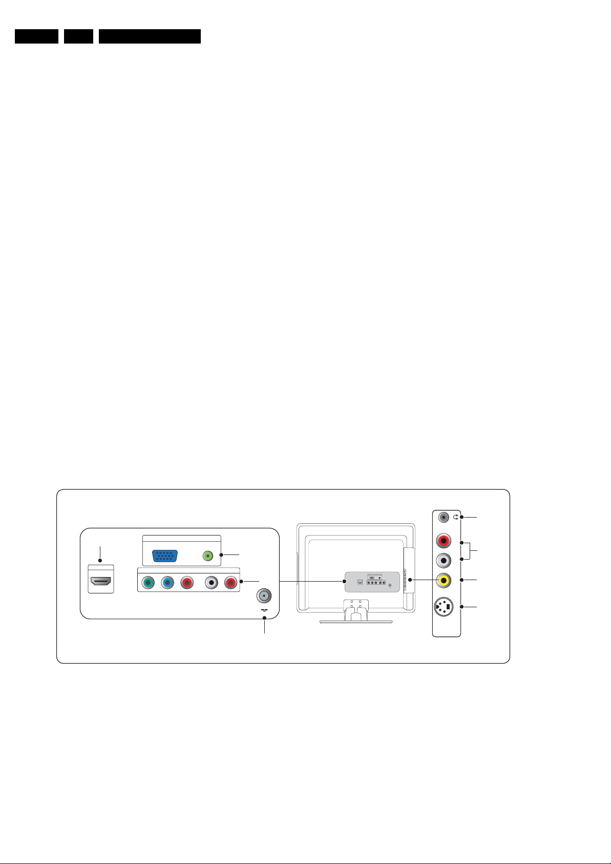
1.2 Connection Overview
1.2.1 Rear and Side Connections
1
HDMI
YPbPr LR
PC IN
VGA AUDIO IN
CVI
2
3
75 Ω
4
Figure 1-1 Rear and Side I/O
HDMI
PC IN
VGA AUDIO IN
CVI
YPbPr LR
5
6
L-AUDIO-RVIDEO IN
75 Ω
SIDE AV
7
8
S-VIDEO
I_17590_051.eps
300508
Page 3
Technical Specifications, Connections, and Chassis Overview
EN 3TPS1.2A LA 1.
1.2.2 Rear Connections
Note: The following connector colour abbreviations are used
(acc. to DIN/IEC 757): Bk= Black, Bu= Blue, Gn= Green, Gy=
Grey, Rd= Red, Wh= White, and Ye= Yellow.
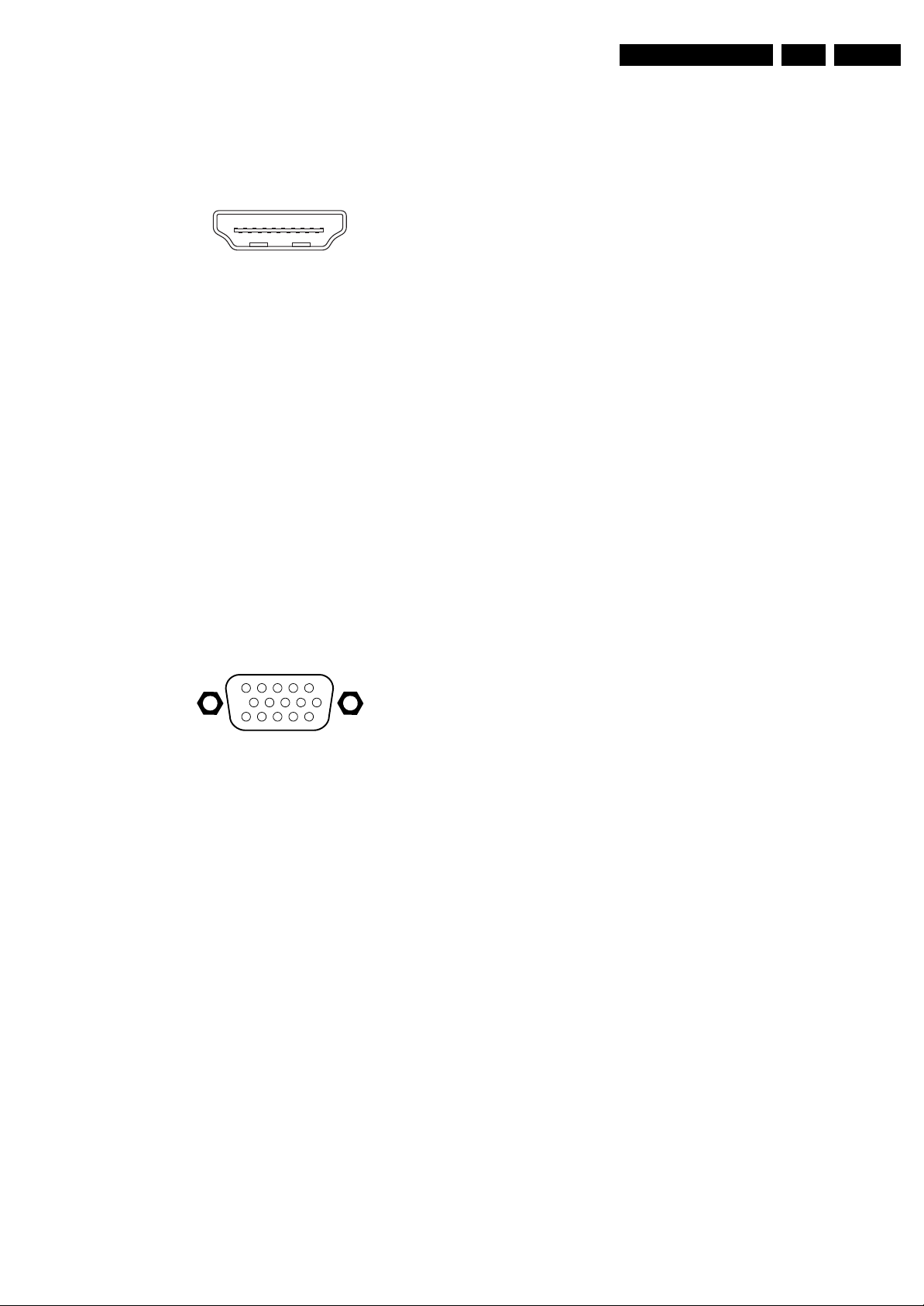
1. HDMI: Digital Video, Digital Audio - In
19
18 2
1
E_06532_017.eps
250505
Figure 1-2 HDMI (type A) connector
1 -D2+ Data channel j
2 -Shield Gnd H
3 -D2- Data channel j
4 -D1+ Data channel j
5 -Shield Gnd H
6 -D1- Data channel j
7 -D0+ Data channel j
8 -Shield Gnd H
9 -D0- Data channel j
10 - CLK+ Data channel j
11 - Shield Gnd H
12 - CLK- Data channel j
13 - CEC
14 - n.c.
15 - DDC_SCL DDC clock j
16 - DDC_SDA DDC data jk
17 - Ground Gnd H
18 - +5V j
19 - HPD Hot Plug Detect j
20 - Ground Gnd H
4. Aerial - In
- - IEC-type (EU) Coax, 75 ohm D
5. Side AV: Audio Head phone- Out
Bk - Head phone 32 - 600 ohm / 10 mW rt
6. Side AV: Audio - In
Wh - Audio L 0.5 V
Rd - Audio R 0.5 V
/ 10 kohm jq
RMS
/ 10 kohm jq
RMS
7. Side AV: Video CVBS - In
Ye - Video CVBS 1 V
/ 75 ohm jq
PP
8. Side AV: Video Y/C - In
1 -Ground Y Gnd H
2 -Ground C Gnd H
3 -Video Y 1 V
4 -Video C 0.3 V
/ 75 ohm j
PP
P / 75 ohm j
PP
2. PC In: Video RGB - In
1
6
11
5
10
15
E_06532_002.eps
050404
Figure 1-3 VGA Connector
1 -Video Red 0.7 V
2 -Video Green 0.7 V
3 -Video Blue 0.7 V
4-n.c.
/ 75 ohm j
PP
/ 75 ohm j
PP
/ 75 ohm j
PP
5 -Ground Gnd H
6 -Ground Red Gnd H
7 -Ground Green Gnd H
8 -Ground Blue Gnd H
9-+5V
10 - Ground Sync Gnd H
+5 V j
DC
11 - n.c.
12 - DDC_SDA DDC data j
13 - H-sync 0 - 5 V j
14 - V-sync 0 - 5 V j
15 - DDC_SCL DDC clock j
2. PC In: Audio - In
Bk - Audio L 0.5 V
Bk - Audio R 0.5 V
/ 10 kohm jq
RMS
/ 10 kohm jq
RMS
3. CVI: Video YPbPr - In, Audio - In
Gn - Video Y 1 V
Bu - Video Pb 0.7 V
Rd - Video Pr 0.7 V
Wh - Audio L 0.5 V
Rd - Audio R 0.5 V
/ 75 ohm jq
PP
/ 75 ohm jq
PP
/ 75 ohm jq
PP
/ 10 kohm jq
RMS
/ 10 kohm jq
RMS
Page 4
EN 4 TPS1.2A LA1.
1.3 Chassis Overview
Technical Specifications, Connections, and Chassis Overview
Figure 1-4 Chassis Overview
I_17590_007.eps
260508
Page 5

Safety Instructions, Warnings, and Notes
2. Safety Instructions, Warnings, and Notes
EN 5TPS1.2A LA 2.
Index of this chapter:
2.1 Safety Instructions
2.2 Warnings
2.3 Notes
2.1 Safety Instructions
Safety regulations require the following during a repair:
• Connect the set to the Mains/AC Power via an isolation
transformer (> 800 VA).
• Replace safety components, indicated by the symbol h,
only by components identical to the original ones. Any
other component substitution (other than original type) may
increase risk of fire or electrical shock hazard.
Safety regulations require that after a repair, the set must be
returned in its original condition. Pay in particular attention to
the following points:
• Route the wire trees correctly and fix them with the
mounted cable clamps.
• Check the insulation of the Mains/AC Power lead for
external damage.
• Check the strain relief of the Mains/AC Power cord for
proper function.
• Check the electrical DC resistance between the Mains/AC
Power plug and the secondary side (only for sets that have
a Mains/AC Power isolated power supply):
1. Unplug the Mains/AC Power cord and connect a wire
between the two pins of the Mains/AC Power plug.
2. Set the Mains/AC Power switch to the “on” position
(keep the Mains/AC Power cord unplugged!).
3. Measure the resistance value between the pins of the
Mains/AC Power plug and the metal shielding of the
tuner or the aerial connection on the set. The reading
should be between 4.5 MΩ and 12 MΩ.
4. Switch “off” the set, and remove the wire between the
two pins of the Mains/AC Power plug.
• Check the cabinet for defects, to prevent touching of any
inner parts by the customer.
2.2 Warnings
• All ICs and many other semiconductors are susceptible to
electrostatic discharges (ESD w). Careless handling
during repair can reduce life drastically. Make sure that,
during repair, you are connected with the same potential as
the mass of the set by a wristband with resistance. Keep
components and tools also at this same potential.
• Be careful during measurements in the high voltage
section.
• Never replace modules or other components while the unit
is switched “on”.
• When you align the set, use plastic rather than metal tools.
This will prevent any short circuits and the danger of a
circuit becoming unstable.
2.3 Notes
2.3.1 General
• Measure the voltages and waveforms with regard to the
chassis (= tuner) ground (H), or hot ground (I), depending
on the tested area of circuitry. The voltages and waveforms
shown in the diagrams are indicative. Measure them in the
Service Default Mode (see chapter 5) with a colour bar
signal and stereo sound (L: 3 kHz, R: 1 kHz unless stated
otherwise) and picture carrier at 475.25 MHz for PAL, or
61.25 MHz for NTSC (channel 3).
• Where necessary, measure the waveforms and voltages
with (D) and without (E) aerial signal. Measure the
voltages in the power supply section both in normal
operation (G) and in stand-by (F). These values are
indicated by means of the appropriate symbols.
2.3.2 Schematic Notes
• All resistor values are in ohms, and the value multiplier is
often used to indicate the decimal point location (e.g. 2K2
indicates 2.2 kΩ).
• Resistor values with no multiplier may be indicated with
either an “E” or an “R” (e.g. 220E or 220R indicates 220 Ω).
• All capacitor values are given in micro-farads (μ=× 10
nano-farads (n =× 10
• Capacitor values may also use the value multiplier as the
decimal point indication (e.g. 2p2 indicates 2.2 pF).
• An “asterisk” (*) indicates component usage varies. Refer
to the diversity tables for the correct values.
• The correct component values are listed in the Spare Parts
List. Therefore, always check this list when there is any
doubt.
2.3.3 BGA (Ball Grid Array) ICs
Introduction
For more information on how to handle BGA devices, visit this
URL: www.atyourservice.ce.philips.com (needs subscription,
not available for all regions). After login, select “Magazine”,
then go to “Repair downloads”. Here you will find Information
on how to deal with BGA-ICs.
BGA Temperature Profiles
For BGA-ICs, you must use the correct temperature-profile,
which is coupled to the 12NC. For an overview of these profiles,
visit the website www.atyourservice.ce.philips.com (needs
subscription, but is not available for all regions)
You will find this and more technical information within the
“Magazine”, chapter “Repair downloads”.
For additional questions please contact your local repair help
desk.
2.3.4 Lead-free Soldering
Due to lead-free technology some rules have to be respected
by the workshop during a repair:
• Use only lead-free soldering tin Philips SAC305 with order
code 0622 149 00106. If lead-free solder paste is required,
please contact the manufacturer of your soldering
equipment. In general, use of solder paste within
workshops should be avoided because paste is not easy to
store and to handle.
• Use only adequate solder tools applicable for lead-free
soldering tin. The solder tool must be able:
– To reach a solder-tip temperature of at least 400°C.
– To stabilize the adjusted temperature at the solder-tip.
– To exchange solder-tips for different applications.
• Adjust your solder tool so that a temperature of around
360°C - 380°C is reached and stabilized at the solder joint.
Heating time of the solder-joint should not exceed ~ 4 sec.
Avoid temperatures above 400°C, otherwise wear-out of
tips will increase drastically and flux-fluid will be destroyed.
To avoid wear-out of tips, switch “off” unused equipment or
reduce heat.
• Mix of lead-free soldering tin/parts with leaded soldering
tin/parts is possible but PHILIPS recommends strongly to
avoid mixed regimes. If this cannot be avoided, carefully
clear the solder-joint from old tin and re-solder with new tin.
-9
), or pico-farads (p =× 10
-12
-6
),
).
Page 6

EN 6 TPS1.2A LA3.
2.3.5 Alternative BOM identification
Note: on the European Service website, “Alternative BOM” is
referred to as “Design variant”.
The third digit in the serial number (example:
AG2B0335000001) indicates the number of the alternative
B.O.M. (Bill Of Materials) that has been used for producing the
specific TV set. In general, it is possible that the same TV
model on the market is produced with e.g. two different types
of displays, coming from two different suppliers. This will then
result in sets which have the same CTN (Commercial Type
Number; e.g. 28PW9515/12) but which have a different B.O.M.
number.
By looking at the third digit of the serial number, one can
identify which B.O.M. is used for the TV set he is working with.
If the third digit of the serial number contains the number “1”
(example: AG1B033500001), then the TV set has been
manufactured according to B.O.M. number 1. If the third digit is
a “2” (example: AG2B0335000001), then the set has been
produced according to B.O.M. no. 2. This is important for
ordering the correct spare parts!
For the third digit, the numbers 1...9 and the characters A...Z
can be used, so in total: 9 plus 26= 35 different B.O.M.s can be
indicated by the third digit of the serial number.
Identification: The bottom line of a type plate gives a 14-digit
serial number. Digits 1 and 2 refer to the production centre (e.g.
AG is Bruges), digit 3 refers to the B.O.M. code, digit 4 refers
to the Service version change code, digits 5 and 6 refer to the
production year, and digits 7 and 8 refer to production week (in
example below it is 2006 week 17). The 6 last digits contain the
serial number.
Directions for Use
MODEL :
PROD.NO:
32PF9968/10
AG 1A0617 000001
MADE IN BELGIUM
220-240V 50/60Hz
~
VHF+S+H+UHF
S
128W
BJ3.0E LA
E_06532_024.eps
260308
Figure 2-1 Serial number (example)
2.3.6 Board Level Repair (BLR) or Component Level Repair (CLR)
If a board is defective, consult your repair procedure to decide
if the board has to be exchanged or if it should be repaired on
component level.
If your repair procedure says the board should be exchanged
completely, do not solder on the defective board. Otherwise, it
cannot be returned to the O.E.M. supplier for back charging!
2.3.7 Practical Service Precautions
• It makes sense to avoid exposure to electrical shock.
While some sources are expected to have a possible
dangerous impact, others of quite high potential are of
limited current and are sometimes held in less regard.
• Always respect voltages. While some may not be
dangerous in themselves, they can cause unexpected
reactions that are best avoided. Before reaching into a
powered TV set, it is best to test the high voltage insulation.
It is easy to do, and is a good service precaution.
3. Directions for Use
You can download this information from the following websites:
http://www.philips.com/support
http://www.p4c.philips.com
Page 7
4. Mechanical Instructions
Index of this chapter:
1. Cable Dressing
2. Service Positions
3. Assy/Panel Removal
4. Re-assembly
Notes:
• Figures below can deviate slightly from the actual situation,
due to the different set executions.
• Follow the disassembly instructions in the described order.
4.1 Cable Dressing
Mechanical Instructions
EN 7TPS1.2A LA 4.
Figure 4-1 Cable dressing
I_17590_008.eps
260508
Page 8
EN 8 TPS1.2A LA4.
Mechanical Instructions
4.2 Service Positions
For easy servicing of this set, there are a few possibilities
created:
• The buffers from the packaging (see figure “Rear cover”).
• Foam bars (created for Service).
4.2.1 Foam Bars
Required for sets
1
42"
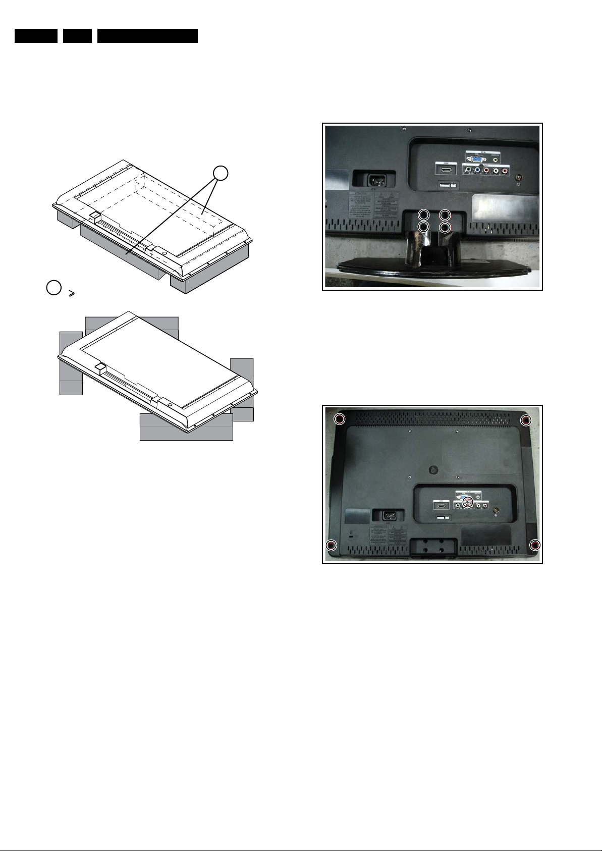
4.3 Assy/Panel Removal
4.3.1 Base
Remove the marked screws to remove the base.
1
I_17591_003.eps
240608
Figure 4-3 Remove Base
4.3.2 Rear Cover
E_06532_018.eps
171106
Figure 4-2 Foam bars
The foam bars (order code 3122 785 90580 for two pieces) can
be used for all types and sizes of Flat TVs. See figure “Foam
bars” for details. Sets with a display of 42” and larger, require
four foam bars [1]. Ensure that the foam bars are always
supporting the cabinet and never only the display.
Caution: Failure to follow these guidelines can seriously
damage the display!
By laying the TV face down on the (ESD protective) foam bars,
a stable situation is created to perform measurements and
alignments. By placing a mirror under the TV, you can monitor
the screen.
1. Remove the marked screws, which secure the rear cover.
2. Lift the rear cover from the cabinet. Make sure that wires
and flat foils are not damaged during cover removal.
I_17591_004.eps
240608
Figure 4-4 Remove rear cover
Page 9
Mechanical Instructions
EN 9TPS1.2A LA 4.
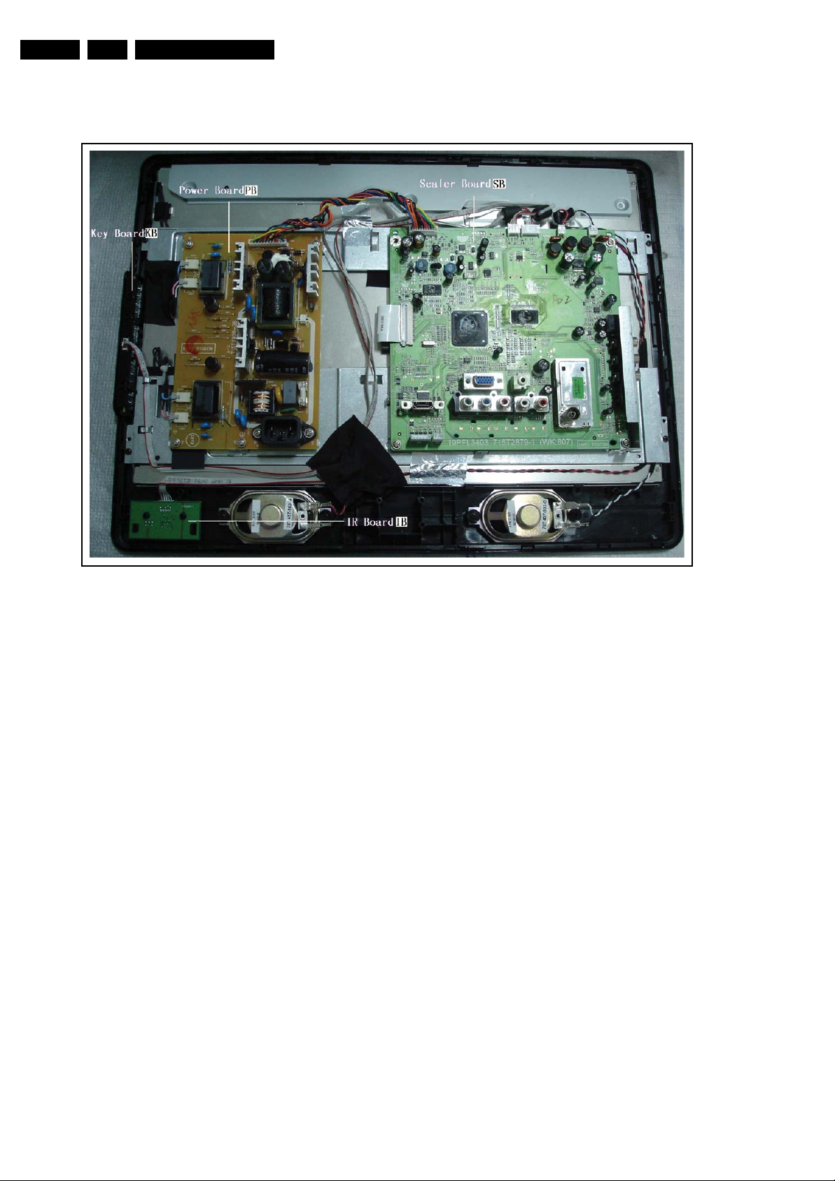
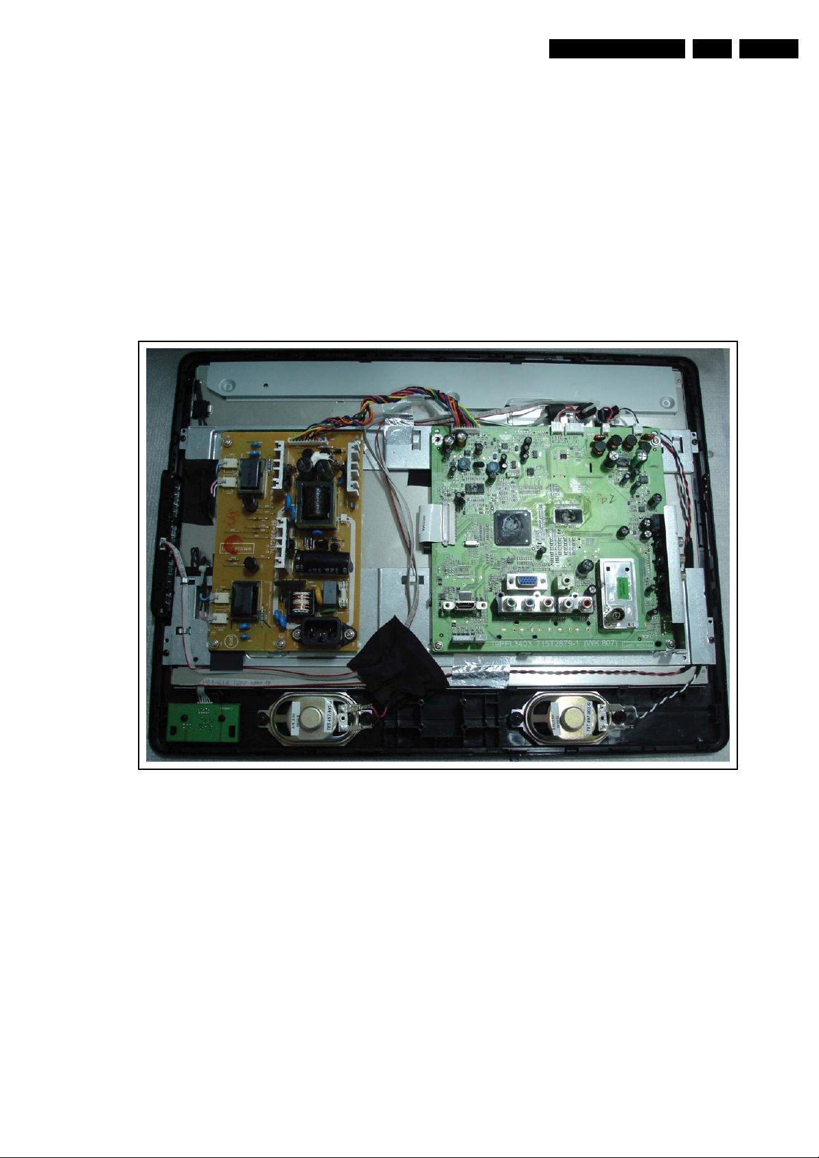
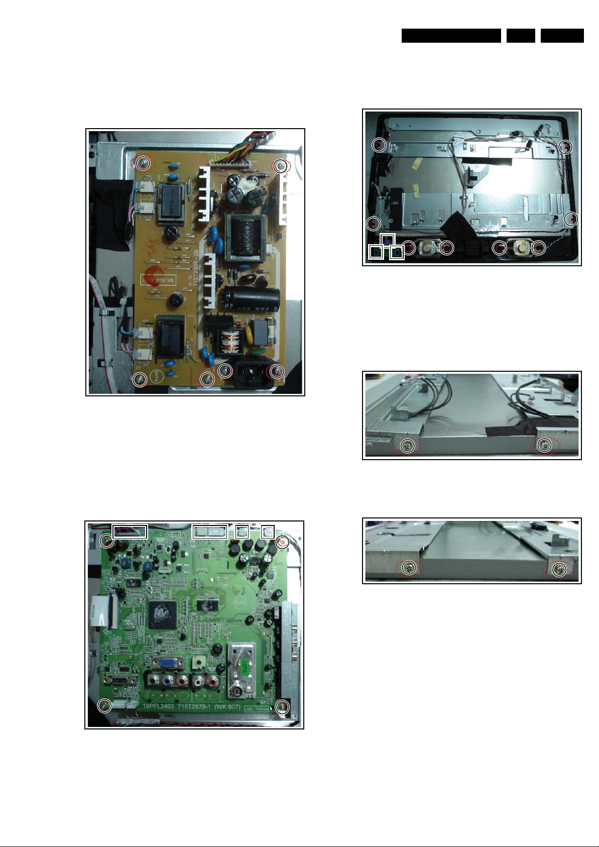
4.3.3 Power Board
1. Refer to next figure.
2. Unplug the marked connectors.
3. Remove the marked screws to remove the Power board.
When defective, replace the whole unit.
4.3.5 Bezel
1. Refer to next figures.
2. Remove the marked screws to remove the bezel.
Figure 4-7 Bezel
4.3.6 Bracket
1. Refer to next two figures.
2. Remove the marked screws to remove the brackets.
I_17590_013.eps
260508
Figure 4-5 Power Board
4.3.4 Scaler Board
1. Refer to next figure.
2. Unplug the marked connectors.
3. Remove the marked screws to remove the Scaler board.
When defective, replace the whole unit.
I_17590_011.eps
260508
Figure 4-8 Bracket 1/2
Figure 4-9 Bracket 2/2
4.4 Set Re-assembly
To re-assemble the whole set, execute all processes in reverse
order.
I_17590_014.eps
260508
I_17590_015.eps
260508
Figure 4-6 Scaler Board
I_17590_012.eps
260508
Notes:
• While re-assembling, make sure that all cables are placed
and connected in their original position. See figure “Cable
dressing”.
Page 10
EN 10 TPS1.2A LA5.
Service Modes, Error Codes, and Fault Finding
5. Service Modes, Error Codes, and Fault Finding
Index of this chapter:
5.1 Test Points
5.2 Service Mode
5.3 Service Tools
5.4 Tips and Tricks
5.1 Test Points
This chassis is not equipped with test points in the service
printing.
5.2 Service Mode
5.2.1 Factory Mode
How to Enter
To enter the Factory mode, please use the following method:
• Press the remote control codes ”062596” + ”STATUS/
EXIT”. Then select “2K8 CH V1 06” in the menu and press
“OK” in order to enter the factory mode.
Caution: This function is meant for development and
service personnel only, not for end customers.
After entering the factory mode, the following screen is visible.
You can now select one of them and press OK.
Figure 5-3 Factory mode menu 2
I_17590_017.eps
260508
I_17590_016.eps
Figure 5-1 Factory mode menu 1 (19PFL3403/93)
260508
How to EXIT
Choose ‘EXIT”, then press “MENU” button on the remote
control.
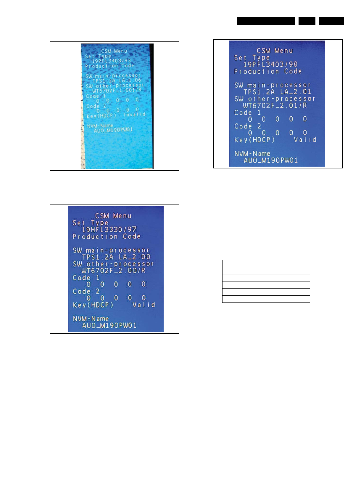
5.2.2 Customer Service Mode (CSM)
Purpose
When a customer is having problems with his TV-set, he can
call his dealer or the Customer Help desk. The service
technician can then ask the customer to activate the CSM in
order to identify the status of the set. Now, the service
technician can judge the severity of the complaint. In many
cases, he can advise the customer how to solve the problem,
or he can decide if it is necessary to visit the customer. The
CSM is read only mode; therefore, modifications in this mode
are not possible.
How to Activate CSM
Key in the codes ”123654” via the standard RC transmitter to
enter the Customer Service Mode.
How to Navigate
By mean of the “CURSOR-DOWN/UP” knob on the RCtransmitter on the screen.
I_17591_005.eps
240608
Figure 5-2 Factory mode menu 1 (19PFL3403/987& 19HFL3330/97)
Page 11
Contents of CSM
Service Modes, Error Codes, and Fault Finding
EN 11TPS1.2A LA 5.
Figure 5-4 CSM Menu (19PFL3403/93)
Figure 5-5 CSM Menu (19HFL3330/97)
I_17590_018.eps
260508
I_17591_006.eps
240608
I_17591_007.eps
240608
Figure 5-6 CSM Menu (19PFL3403/98)
Menu Explanation
1. Set Type: Type number and region.
2. Production code: Product serial no.
3. SW main-processor: SW-naming of Mstar/Trident.
4. SW other-processor: SW-naming of MCU.
5. Code 1: Logging I2C error codes in NVM/EEPROM (5 last
logged errors).
6. Code 2: Logging I2C error codes in NVM/EEPROM (5 first
logged errors).
For the error codes, please refer to the table below.
Error Code Error Code Type
0x01 Audio decoder error
0x02 I2C bus error
0x03 Tuner error
0x04 NVRAM error
0x05 Scaler chip error
7. Key (HDCP): Indicates if the HDCP-key is valid.
8. NVM-Naming: Indicates the used LCD panel type and
region (NVM content and main SW depend on the used
LCD panel).
How to exit
Press ”MENU” on the RC-transmitter.
Page 12
EN 12 TPS1.2A LA5.
Service Modes, Error Codes, and Fault Finding
5.3 Service Tools
5.3.1 ComPair
Introduction
ComPair (Computer Aided Repair) is a Service tool for Philips
Consumer Electronics products. And offers the following:
1. ComPair helps you to quickly get an understanding on how
to repair the chassis in a short and effective way.
2. ComPair allows very detailed diagnostics and is therefore
capable of accurately indicating problem areas. You do not
have to know anything about I
yourself, because ComPair takes care of this.
3. ComPair speeds up the repair time since it can
automatically communicate with the chassis (when the uP
is working) and all repair information is directly available.
4. ComPair features TV software upgrade possibilities.
Specifications
ComPair consists of a Windows based fault finding program
and an interface box between PC and the (defective) product.
The (new) ComPair II interface box is connected to the PC via
a USB cable. For the TV chassis, the ComPair interface box
and the TV communicate via a bi-directional cable via the
service connector(s).
How to Connect
This is described in the ComPair chassis fault finding database.
TO
UART SERVICE
CONNECTOR
2
C or UART commands
TO TV
TO
I2C SERVICE
CONNECTOR
TO
UART SERVICE
CONNECTOR
5.3.2 LVDS Tool
Support of the LVDS Tool has been discontinued.
5.4 Tips and Tricks
Below find some repair tips and tricks.
5.4.1 Soft Reset
When a consumer has forgotten his lock code, you can set the
TV back in Virgin mode by keying in the code”978450” via the
standard RC transmitter. The NVM is not erased.
The standard unlock code will then be “0711”.
5.4.2 Hard Reset (erase NVRAM)
A hard reset is executed by together pressing the “P+” and “V+”
buttons on the TV, while unplugging and replugging the mains
cord.
Note: By using this hard reset mode, the TV will be brought
back in Virgin mode, but also all TV settings will be erased!
TV must completely be re-aligned via the “Factory” mode.
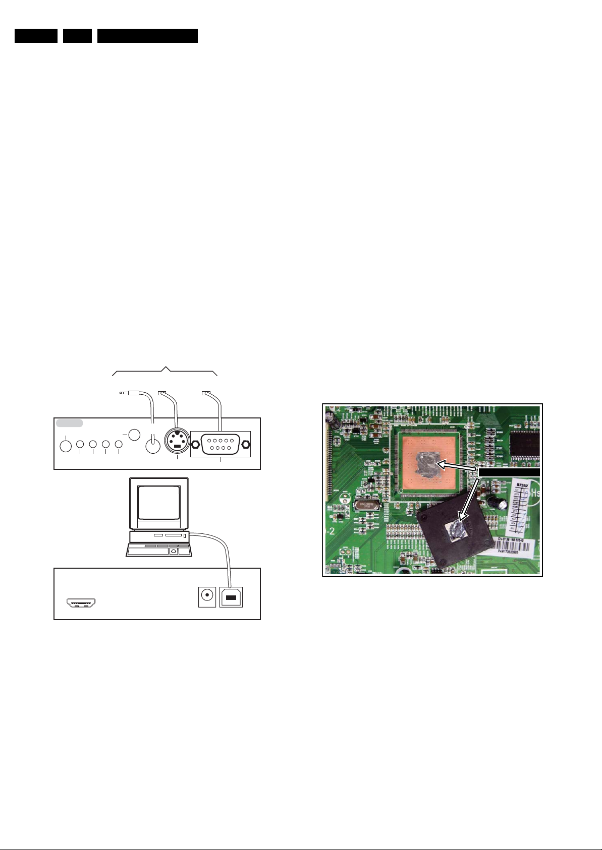
5.4.3 Removal of Morning Star Microprocessor
The Morning Star uP is fitted with a so-called E-pad (see photo
below). This is an extra surface for cooling and grounding. This
E-pad is soldered to the PWB.
To remove/place this IC on the PWB, use dedicated
equipment.
ComPair II
RC in
Optional
Switch
Power ModeLink/
Activity
RC out
Multi
function
2
C
I
RS232 /UART
PC
ComPair II Developed by Philips Brugge
Optional power
HDMI
2
C only
I
5V DC
E_06532_036.eps
150208
Figure 5-7 ComPair II interface connection
Caution: It is compulsory to connect the TV to the PC as
shown in the picture above (with the ComPair interface in
between), as the ComPair interface acts as a level shifter. If
one connects the TV directly to the PC (via UART), ICs will be
blown!
Soldered E-Pad
I_17620_046.eps
Figure 5-8 E-pad (photo from TPS1.0 chassis)
280308
How to Order
ComPair II order codes:
• ComPair II interface: 3122 785 91020.
• For SW see Philips service website.
• ComPair UART interface cable: 3122 785 90630.
Note: If you encounter any problems, contact your local
support desk.
Page 13
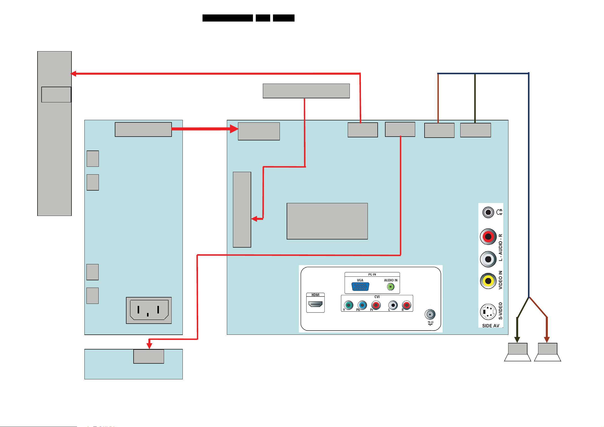
Block Diagrams, Test Point Overview, and Waveforms
6. Block Diagrams, Test Point Overview, and Waveforms
Wiring Diagram
13TPS1.2A LA 6.
Key
Board
4 Pin
CN0101
095T8013 2X912
4
095T8014 4X912
095T8013 2X911
Panel
1
CN7302
12 Pin
1
CN902
CN825
CN824
Power Board
12
11
CN7502
11 Pin
CN7201
30
30 Pin
1
089T179E30C921
MST98980CLD-LF
FFC Cable
U4201
4 Pin
4
CN7301
1
7 Pin
7
2 Pin 2Pin
1
2121
CN6101
CN6102
HEADPHONE
CN823
CN821
IR Board
AC IN
CN901
1
5 Pin
CN0201
1
AUDIO R/L
095T8014 7X909
VIDEO
S-VIDEO
5
Speaker R/L
I_17591_001.eps
230608
Page 14
Block Diagrams, Test Point Overview, and Waveforms
Block Diagram Scaler Board
PHILIPS 19W Block Diagram
14TPS1.2A LA 6.
Video Block
Tuner PACK
CVI
S_VIDEO
VGA
HDMI
MAIN_AV_CVBS
SIDE _AV_CVBS
SB-03
SB-04
SB-05
SB-06
SB-07
SB-04
SB-05
Tuner_CVBS
YPbPr
Y/C
PC(R,G,B&H,V)
WT6702F_S240
(Sub MCU)
SB-09
MST98980CLD
MST98980CLD
HY57V641620FTP-6-C
(SDRAM)
SB-11
SB-12
SB-12
SB-11
2
I
C BUS
LVDS to panel
M190PW01 V000
CTOC AUO
SB-14
Inverter Power
SB-02
KEY/IR
IR Receiver LED
Flash /93 :MX25L4005AM2C-12G
/98:MX25L8005M2I-15G
SB-10 EEPROM M24C32-WMN6TP
Audio Block
Tuner_SIF
CVI L/R
MAIN AV
PC AUDIO
HDMI
SIDE AV
SB-03
SB-04
SB-04
SB-15
SB-07
SB-05
TV
TV
CONTROLLER
CONTROLLER
SB-10
SB-16
EARPHONE AMP
TDA7491LP13TR
SB-16
Headphone
speakers
I_17591_002.eps
230608
Page 15
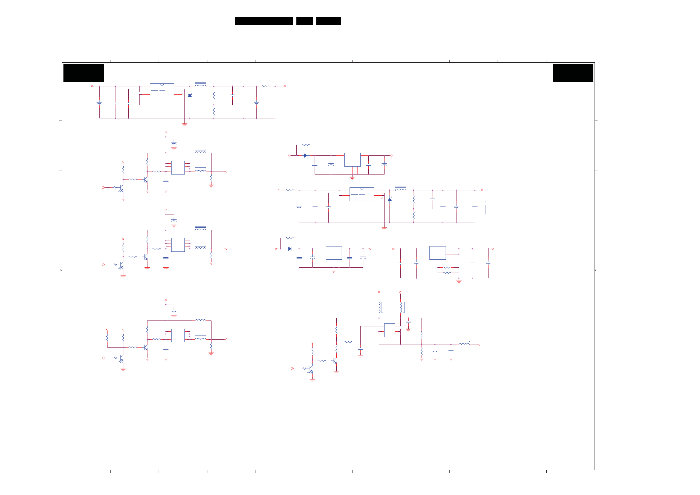
Circuit Diagrams and PWB Layouts
7. Circuit Diagrams and PWB Layouts
15TPS1.2A LA 7.
Scaler Board: DC-DC Power
1
2
3
4
5
6
7
8
9
10
11
DC-DC POWER
SB01
A
B B
C C
D
E
F F
+
+
5V_PWR_SWSB09
5V_PWR_SW1SB10
+5V_STBY
12V_PWR_SWSB9,10
C7101
C7101
47uF 25V
47uF 25V
2
2
R7127
R7127
47K(NC)
47K(NC)
2
C7102
C7102
0.1uF
0.1uF
+5V_STBY
1 3
+5V_SW
1 3
+5V_SW
1 3
C7103
C7103
0.1uF
0.1uF
R7123
R7123
47K
47K
R71241KR7124
1K
Q7101
Q7101
MUN2211T
MUN2211T
R7125
R7125
47K
47K
R71261KR7126
1K
Q7103
Q7103
MUN2211T
MUN2211T
R7136
R7136
47K(NC)
47K(NC)
R7128
R7128
1K(NC)
1K(NC)
Q7105
Q7105
MUN2211T(NC)
MUN2211T(NC)
R7102
R7102
56K
56K
2
R7105
R7105
56K
56K
2
R7108
R7108
56K(NC)
56K(NC)
2
U7101
U7101
AIC1550POTR
AIC1550POTR
1
VIN
2
BP
3
SHDN
4
FB
R7103
R7103
3
Q7109
Q7109
BC847C
BC847C
1
R7106
R7106
3
Q7110
Q7110
BC847C
BC847C
1
R7109
R7109
100K(NC)
100K(NC)
3
Q7111
Q7111
BC847C(NC)
BC847C(NC)
1
56K
56K
100K
100K
MODE/
MODE/
SYNC
+5V_STBY
+5V_STBY
+12V_STBY
8
LX
7
GND
6
5
RT
+
+
C7107
C7107
100UF 25V
100UF 25V
Q7102
Q7102
1
S
2
S
3
S
4
G
SI4835BDY
SI4835BDY
C7106
C7106
100N 50V
100N 50V
+
+
C7110
C7110
100UF 25V
100UF 25V
Q7104
Q7104
1
S
2
S
3
S
4
G
SI4835BDY
SI4835BDY
C7109
C7109
220N 25V
220N 25V
+
+
C7113
C7113
100UF 25V(NC)
100UF 25V(NC)
Q7106
Q7106
1
S
2
S
3
S
4
G
SI4835BDY(NC)
SI4835BDY(NC)
C7112
C7112
220N 25V(NC)
220N 25V(NC)
D
D
D
D
D
D
D
D
D
D
D
D
ZD7102
ZD7102
SSA34-E3(NC)
SSA34-E3(NC)
1 2
1 2
8
7
6
1 2
5
1 2
8
7
6
1
5
1
8
7
6
5
1 2
L7102
L7102
6.8uH
6.8uH
FB7101
FB7101
120R(NC)
120R(NC)
FB7102
FB7102
120R
120R
FB7103
FB7103
120R(NC)
120R(NC)
FB7104
FB7104
120R
120R
FB7105
FB7105
120R(NC)
120R(NC)
FB7106
FB7106
120R(NC)
120R(NC)
R7101
R7101
0R05
C7137
C7137
4.7UF
4.7UF
0R05
+
+
C7138
C7138
47UF 25V
47UF 25V
+5V_SW1
+5V_SW
R7134
R7134
560K 1%
560K 1%
R7135
R7135
162K 1%
162K 1%
R7104
R7104
10K
10K
2
R7107
R7107
10K
10K
2
R7110
R7110
10K(NC)
10K(NC)
+5V_SW
+5V_SW1
+12V_SW
C7104
C7104
33P
33P
+3V3_STBY+5V_STBY
C7139
C7139
0.1uF
0.1uF
R7111
R7111
0R(NC)
0R(NC)
D7102
D7102
+5V_SW +3V3_SW
R7132
R7132
0R05
0R05
R7114
R7114
0R(NC)
0R(NC)
D7103
D7103
1
K
A
S1D-E3
S1D-E3
SB10
PANEL_PWR
2
A1K
S1D-E3
S1D-E3
C7114
C7114
100N
100N
+
+
C7118
C7118
C7119
C7119
47uF 25V
47uF 25V
0.1uF
0.1uF
U7104
U7104
AME8815AEGT330Z
+
+
C7126
C7126
10uF 50V
10uF 50V
R7129
R7129
47K
47K
Q7107
Q7107
MUN2211T
MUN2211T
1 3
AME8815AEGT330Z
1
R71301KR7130
1K
2
C7125
C7125
0.1uF
0.1uF
+5V_SW
2
U7102
U7102
AME8815AEGT330Z
AME8815AEGT330Z
1
+
+
C7115
C7115
10UF/50V
10UF/50V
C7120
C7120
0.1uF
0.1uF
3
VOUT
VIN
GND
TH
2
4
R7121
R7121
56K
56K
R7133
R7133
0R05
0R05
3
Q7112
Q7112
2
BC847C
BC847C
1
VIN
U7103
U7103
AIC1550POTR
AIC1550POTR
1
VIN
2
BP
3
SHDN
4
FB
R7122
R7122
75K
75K
VOUT
GND
2
C7127
C7127
0.1uF
0.1uF
TH
4
3
MODE/
MODE/
GND
SYNC
+
+
C7128
C7128
100uF 10V
100uF 10V
C7133
C7133
0.1u 25V
0.1u 25V
C7116
C7116
100N
100N
LX
RT
+3V3
+12V_STBY
8
7
6
5
+5V_SW1
12
4
3
2
1
FB7107
FB7107
120R(NC)
120R(NC)
Q7108
Q7108
SI5441DC
SI5441DC
+
+
C7117
C7117
100uF 10V
100uF 10V
ZD7101
ZD7101
SSA34-E3(NC)
SSA34-E3(NC)
1 2
S
G
D
D
D
D
D
D
L7101
L7101
15uH
15uH
+5V_STBY
12
5
6
7
8
C7129
C7129
0.1uF(NC)
0.1uF(NC)
FB7108
FB7108
120R
120R
C7134
C7134
0.1uF
0.1uF
R7112
R7112
560K 1%
560K 1%
R7113
R7113
820K 1%
820K 1%
+
+
C7130
C7130
10uF 50V(NC)
10uF 50V(NC)
C7121
C7121
68P
68P
U7105
U7105
AME1117ACGTZ(NC)
AME1117ACGTZ(NC)
3
VIN
VOUT
1
R7137
R7137
0R05(NC)
0R05(NC)
+
+
C7135
C7135
R7131
R7131
10uF 50V
10uF 50V
10K
10K
C7122
C7122
4.7UF
4.7UF
2
4
TH
ADJ
R7115
R7115
100R 1%(NC)
100R 1%(NC)
R7116
R7116
110R 1%(NC)
110R 1%(NC)
+
+
C7123
C7123
100UF/25V
100UF/25V
FB7109
FB7109
1 2
120R
120R
C7136
C7136
0.1uF
0.1uF
C7124
C7124
0.1uF
0.1uF
C7131
C7131
0.1uF(NC)
0.1uF(NC)
PANEL_VCC
+1V2
+2V6
+
+
C7132
C7132
100uF 10V(NC)
100uF 10V(NC)
SB01
A
D
E
C7101 A1
C7102 A2
C7103 A2
C7104 A4
C7106 C3
C7107 B3
C7109 D3
C7110 C3
C7112 F3
C7113 E3
C7114 B6
C7115 B6
C7116 B7
C7117 B7
C7118 C5
C7119 C6
C7120 C6
C7121 C8
C7122 C8
C7123 C9
C7124 C9
C7125 D5
C7126 D6
C7127 D6
C7128 D7
C7129 D7
C7130 D8
C7131 D9
C7132 D9
C7133 F7
C7134 E8
C7135 F8
C7136 F8
C7137 A4
C7138 A4
C7139 A5
D7102 B5
D7103 D5
FB7101 B3
FB7102 B3
FB7103 D3
FB7104 D3
FB7105 E3
FB7106 F3
FB7107 E7
FB7108 E7
FB7109 F9
L7101 C7
L7102 A3
Q7101 C2
Q7102 B3
Q7103 D2
Q7104 D3
Q7105 F2
Q7106 F3
Q7107 F5
Q7108 F7
Q7109 C2
Q7110 D2
Q7111 F2
Q7112 F6
R7101 A5
R7102 B2
R7103 B2
R7104 C3
R7105 D2
R7106 D2
R7107 D3
R7108 F2
R7109 F2
R7110 F3
R7111 B5
R7112 C8
R7113 C8
R7114 D5
R7115 D8
R7116 D8
R7121 F6
R7122 F6
R7123 B2
R7124 C2
R7125 D2
R7126 D2
R7127 F1
R7128 F2
R7129 F6
R7130 F6
R7131 F8
R7132 C5
R7133 F6
R7134 A4
R7135 A4
R7136 F2
R7137 F8
U7101 A2
U7102 B6
U7103 C6
U7104 D6
U7105 D8
ZD7101 C7
ZD7102 A3
G G
H H
I_17590_021.eps
1
2
3
4
5
6
7
8
9
10
260508
11
Page 16
Circuit Diagrams and PWB Layouts
16TPS1.2A LA 7.
Scaler Board: PS & Inverter I/F
1
PS & INVERTER I/F
SB02 SB02
A A
R7205
BL_ADJSB10
B
BL_ENSB10
R7205
R7209
R7209
2
R7201
R7201
4K7(NC)
4K7(NC)
10K
10K
10K
10K
+3V3
2
R7215
R7215
4K7
4K7
2
C7203
C7203
1U(NC)
1U(NC)
+5V_SW1
R7202
R7202
4K7
4K7
3
Q7201
Q7201
BC847C
BC847C
1
+5V_SW1
R7206
R7206
10K
10K
3
Q7202
Q7202
BC847C
BC847C
1
R7203
R7203
R7208
R7208
0R05
0R05
100R
100R
3
R7204
R7204
C7201
C7201
1U(NC)
1U(NC)
INVERTER_ON_OFF
C7204
C7204
0.1uF
0.1uF
10R
10R
C7202
C7202
0.1uF(NC)
0.1uF(NC)
BRIGHT_ADJ
4
5
6
7
8
CN7201 C1
C7201 A3
C7202 A3
C7203 B2
C7204 B3
C7205 C3
C7206 D2
C7207 D3
C7208 D3
C7209 D2
C7210 D3
C7211 D3
FB7201 C2
FB7202 C2
FB7203 C2
FB7204 D2
FB7205 D2
FB7206 D2
Q7201 A2
Q7202 B2
R7201 A2
R7202 A2
R7203 A3
R7204 A3
R7205 A2
R7206 B2
R7208 B3
R7209 B2
B
R7210 C3
R7211 C3
R7212 C3
R7213 C3
R7214 C3
R7215 A2
R7216 D3
R7210
C C
For PS
CN7201
CN7201
1
2
3
4
5
6
7
8
D D
63391 11P 2.0MM
63391 11P 2.0MM
E
9
10
11
1 2
FB7201
FB7201
1 2
FB7202
FB7202
1
FB7203
FB7203
FB7204
FB7204
1
120R
120R
C7206
C7206
0.1uF
0.1uF
FB7205
FB7205
1
120R
120R
C7209
C7209
0.1uF
0.1uF
FB7206
FB7206
1 2
120R
120R
120R
120R
120R
120R
120R
120R
2
R7214
R7214
0R(NC)
0R(NC)
2
2
C7207
C7207
0.1uF
0.1uF
C7210
C7210
0.1uF
0.1uF
R7216
R7216
R7212
R7212
47K
47K
C7208
C7208
+
+
470uF 25V
470uF 25V
C7211
C7211
+
+
470uF 25V
470uF 25V
47R
47R
R7210
R7211
R7211
R7213
R7213
C7205
C7205
0.1uF
0.1uF
+5V_STBY
+12V_STBY
STANDBY SB09
47R
47R
47R
47R
47R
47R
PANEL_ID SB10
INVERTER_ON_OFF
BRIGHT_ADJ
E
I_17590_022.eps
1
2
3
4
5
6
7
8
260508
Page 17
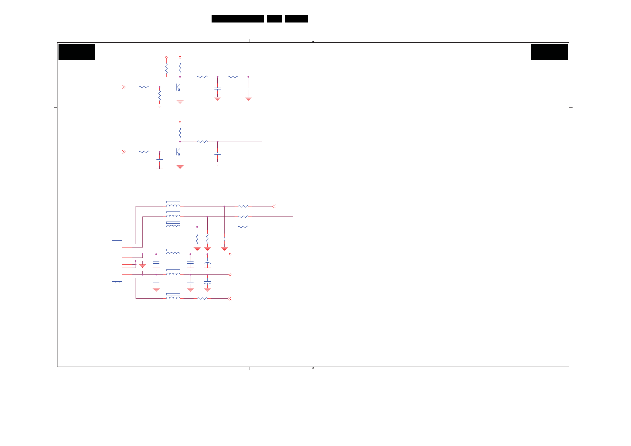
Circuit Diagrams and PWB Layouts
17TPS1.2A LA 7.
Scaler Board: Tuner
1
2
3
4
5
6
7
8
TUNER
SB03 SB03
1234567
A A
ANT IN
ANT IN
+5V3SCL4SDA
N.C.
N.C.
2
1
B B
TH121TH2
NC1NC2+B3NC4AGC5TP(TU)6NC7GND8SDA9SCL10AS11NC12VIDEO OUT13AFT14AUDIO OUT15SIF OUT16NC17NC18NC19NC
100P
100P
47R
47R
47R
47R
C1103
C1103
22
C1102
C1102
0.1uF
0.1uF
+
+
C1101
C1101
2U2 50V
2U2 50V
C1104
C1104
100P
100P
C C
R1101
I2C_SDASB09,10,13
I2C_SCLSB09,10,13
D D
E
R1101
R1102
R1102
AS_TU
6
5
R1104
R1104
0R(NC)
0R(NC)
CN1101
CN1101
63388 8P 2.0MM(NC)
63388 8P 2.0MM(NC)
8
AS_IF102ND IF SOUND
NC
9
R11030RR1103
0R
CVBS
11
12
20
C1105
C1105
330N 16V
330N 16V
L1101
L1101
22uH(NC)
22uH(NC)
FB1101
FB1101
1 2
120R
120R
+
+
C1106
C1106
1000uF 16V
1000uF 16V
R11050RR1105
NC
NC
+5V,IF
13
TU1101
TU1101
TH323TH4
TUNER TAFT-Z017D
TUNER TAFT-Z017D
24
2
0R
TU1102
TU1102
AF O/P
14
+5V_SW1
C1107
C1107
0.1uF
0.1uF
TH1
TH2
TH3
TH4
3
1
15
16
17
18
R1116
R1116
C1109
C1109
+
+
10uF 50V
10uF 50V
R1117
R1117
C1110
C1110
+
+
10uF 50V(NC)
10uF 50V(NC)
R1106
R1106
10K(NC)
10K(NC)
Q1101
Q1101
BC847C(NC)
BC847C(NC)
0R(NC)
0R(NC)
0R(NC)
0R(NC)
TV_CVBS
R1108
R1108
75R 1%
75R 1%
TV_SIF
Mono
R1115
R1115
C1108
C1108
470uF 10V
470uF 10V
R1118
R1118
75R 1%(NC)
75R 1%(NC)
R1110
R1110
2K2(NC)
2K2(NC)
10K(NC)
10K(NC)
TU1101
TU1102
+
+
0R(NC)
0R(NC)
100K(NC)
100K(NC)
R1114
R1114
R1113
R1113
C1101
Ye s
NC
C1114
C1114
22P
22P
C1105
Ye s
NC
1 2
FB110230RFB110230R
C1111
C1111
330P(NC)
330P(NC)
C1118
C1118
100P(NC)
100P(NC)
C1108
Ye s
NC
C1109
Ye s
NC
C1112
C1112
330P(NC)
330P(NC)
R1116
NC
Ye s
R1118
NC
Ye s
R1109
R1109
R11110RR1111
R11120RR1112
47R
47R
0R
0R
C1117
C1117
C1113
C1113
C1115
C1115
C1116
C1116
0.1uF(NC)
0.1uF(NC)
47N
47N
0.1uF
0.1uF
0.1uF
0.1uF
TUNER_CVBS SB10
SIFP0 SB10
SIFM0 SB10
AUMONO SB10
E
CN1101 A2
C1101 C2
C1102 D2
C1103 D2
C1104 D2
C1105 C3
C1106 D3
C1107 D3
C1108 C5
C1109 D4
C1110 D4
C1111 C5
C1112 C6
C1113 C6
C1114 D5
C1115 D6
C1116 D6
C1117 D6
C1118 D5
FB1101 D3
FB1102 C5
L1101 D3
Q1101 E3
R1101 C1
R1102 C1
R1103 D2
R1104 D2
R1105 E3
R1106 D3
R1107 E3
R1108 C4
R1109 C6
R1110 D4
R1111 D6
R1112 D6
R1113 D5
R1114 C5
R1115 D4
R1116 C4
R1117 D4
R1118 C5
TU1101 B1
TU1102 A1
R1107
R1107
10K(NC)
10K(NC)
I_17590_023.eps
1
2
3
4
5
6
7
8
260508
Page 18

Circuit Diagrams and PWB Layouts
18TPS1.2A LA 7.
Scaler Board: Video Input 1
1
SB04 SB04
A
VIDEO INPUT 1
2
3
4
5
6
7
8
9
10
11
For MM/DVB-T Module IN
CN1201
CN1201
B
63387 7P 2.0MM(NC)
C C
D D
63387 7P 2.0MM(NC)
1
2
3
4
5
6
7
CN1202
CN1202
RCA JACK 1x3V GBR
RCA JACK 1x3V GBR
2
1
4
3
6
5
R_PR2
G_Y2
B_PB2
75R 1%(NC)
75R 1%(NC)
AV_AU_INL
AV_AU_INR
PR1
Y1
PB1
75R 1%
75R 1%
R1201
R1201
R1208
R1208
1
FB1201
FB1201
1
FB1204
FB1204
30R(NC)
30R(NC)
C1201
C1201
10P(NC)
10P(NC)
C1208
C1208
10P(NC)
10P(NC)
2
R1202
R1202
75R 1%(NC)
75R 1%(NC)
2
30R
30R
R1209
R1209
75R 1%
75R 1%
1
FB1202
FB1202
C1202
C1202
10P(NC)
10P(NC)
1 2
FB1205
FB1205
C1209
C1209
10P(NC)
10P(NC)
30R(NC)
30R(NC)
75R 1%(NC)
75R 1%(NC)
2
R1203
R1203
30R
30R
R1210
R1210
75R 1%
75R 1%
1 2
FB1203
30R(NC)
FB1203
30R(NC)
C1203
C1203
10P(NC)
10P(NC)
1 2
FB1206
FB1206
C1210
C1210
10P(NC)
10P(NC)
30R
30R
R1204
R1204
R1205
R1205
R1206
R1206
R1207
R1207
R1211
R1211
R1212
R1212
R1213
R1213
R1214
R1214
47R(NC)
47R(NC)
47R(NC)
47R(NC)
47R(NC)
47R(NC)
470R(NC)
470R(NC)
47R
47R
47R
47R
47R
47R
470R
470R
C1204 47N(NC)C1204 47N(NC)
C1205 47N(NC)C1205 47N(NC)
C1206 47N(NC)C1206 47N(NC)
C1207 1N(NC)C1207 1N(NC)
C1211
C1211
C1212 47NC1212 47N
C1213 47NC1213 47N
C12141NC1214
47N
47N
1N
PR2+
Y2+
PB2+
SOY2
PR1+
Y1+
PB1+
SOY1
PR2+ SB10
Y2+ SB10
PB2+ SB10
SOY2 SB10
PR1+ SB10
Y1+ SB10
PB1+ SB10
SOY1 SB10
CN1201 A1
CN1202 C1
CN1203 D1
C1201 B2
C1202 B3
C1203 B4
A
C1204 A5
C1205 B5
C1206 B5
C1207 B5
C1208 C2
C1209 C3
C1210 C4
C1211 C5
C1212 C5
C1213 C5
C1214 C5
C1218 D5
B
C1219 D6
C1220 D7
C1222 D2
C1223 D3
C1224 D4
D1205 D5
D1206 D6
D1207 D6
D1208 D7
FB1201 A2
FB1202 A3
FB1203 B4
FB1204 C2
FB1205 C3
FB1206 C4
FB1207 D2
R1201 B2
R1202 B3
R1203 B3
R1204 A4
R1205 B4
R1206 B4
R1207 B4
R1208 C2
R1209 C3
R1210 C3
R1211 C4
R1212 C4
R1213 C4
R1214 C4
R1216 D2
R1217 D3
E E
+3V3_ESD
CN1203
CN1203
RCA JACK 1x3V YWR(NC)
F F
G G
H H
RCA JACK 1x3V YWR(NC)
1
2
1
4
3
6
5
MAIN_AV_CVBS
75R 1%(NC)
75R 1%(NC)
AV_AU_INL
AV_AU_INR
2
R1216
R1216
1 2
FB1207
FB1207
30R(NC)
30R(NC)
C1222
C1222
330P(NC)
330P(NC)
AV_AU_INL SB15
AV_AU_INR SB15
3
R1217
R1217
C1223
C1223
330P(NC)
330P(NC)
47R(NC)
47R(NC)
4
C1224 47N(NC)C1224 47N(NC)
5
AV_CVBS1 SB10
6
D1205
D1205
PR1
3
BAV99(NC)
BAV99(NC)
D1208
9
D1208
3
BAV99(NC)
BAV99(NC)
2
C1220
C1220
0.1uF(NC)
0.1uF(NC)
1
I_17590_024.eps
10
260508
11
D1206
2
C1218
C1218
0.1uF(NC)
0.1uF(NC)
1
7
D1206
Y1 PB1
3
BAV99(NC)
BAV99(NC)
BAS32L(NC)
BAS32L(NC)
8
D1207
D1207
2
C1219
C1219
0.1uF(NC)
0.1uF(NC)
1
2
K
A
1
Page 19

Circuit Diagrams and PWB Layouts
19TPS1.2A LA 7.
Scaler Board: Video Input 2 (Side AV)
SIDE_SV_Y0
11
SIDE_SV_C0
SIDE_AV_CVBS
2
SIDE_AU_INL
SIDE_AU_INR
R1301
R1301
75R 1%
75R 1%
R1303
R1303
75R 1%
75R 1%
R1305
R1305
75R 1%
75R 1%
1 2
FB1301
FB1301
C1301
C1301
330P(NC)
330P(NC)
1 2
FB1302
FB1302
C1304
C1304
330P(NC)
330P(NC)
1 2
FB1303
FB1303
C1307
C1307
330P(NC)
330P(NC)
SIDE_AU_INL SB15
SIDE_AU_INR SB15
1
SB05
A
B
C C
VIDEO INPUT 2 (SIDE AV)
CN1301A
CN1301A
SJACK+RCA1X3H
SJACK+RCA1X3H
12
7 8
CY
CY
9 10
GG
GG
13
CN1301B
CN1301B
SJACK+RCA1X3H
SJACK+RCA1X3H
2
1
4
3
6
5
30R
30R
30R
30R
30R
30R
3
R1302
R1302
C1302
C1302
330P(NC)
330P(NC)
R1304
R1304
C1305
C1305
330P(NC)
330P(NC)
R1306
R1306
C1308
C1308
330P(NC)
330P(NC)
47R
47R
47R
47R
47R
47R
C1303
C1303
C1306 47NC1306 47N
C1309
C1309
47N
47N
47N
47N
4
SV_Y0 SB10
SV_C0 SB10
AV_CVBS0 SB10
5
CN1302
CN1302
1
2
3
4
5
6
7
8
9
10
63390 10P 2.0MM(NC)
63390 10P 2.0MM(NC)
CN1303
CN1303
2SJ1508-001111
2SJ1508-001111
HP_DET_IN
5
4
3
2
7
8
1
R1307
R1307
SIDE_AV_CVBS
SIDE_SV_C0
SIDE_SV_Y0
SIDE_AU_INL
SIDE_AU_INR
HPL
HPR
C1311
C1311
6N8
6N8
100R
100R
HPL SB16
HPR SB16
1 2
FB1304
FB1304
1 2
FB1305
FB1305
C1312
C1312
6N8
6N8
6
C1310
C1310
100P(NC)
100P(NC)
120R
120R
120R
120R
HP_DET SB10
HP_DET_IN
HPR
HPL
7
8
SB05
N1301A A1
N1301B C1
CN1302 B5
CN1303 C5
C1301 B2
C1302 B3
C1303 B4
C1304 B2
C1305 B3
C1306 B4
A
C1307 C2
C1308 C3
C1309 C4
C1310 B6
C1311 C5
C1312 C6
FB1301 B3
FB1302 B3
FB1303 C3
FB1304 C6
FB1305 C6
R1301 B2
R1302 B3
R1303 B2
R1304 B3
R1305 C2
R1306 C3
R1
B
307 A6
D D
E
I_17590_025.eps
1
2
3
4
5
6
7
8
260508
E
Page 20

Circuit Diagrams and PWB Layouts
Scaler Board: D-Sub Input
1
20TPS1.2A LA 7.
2
3
4
5
6
7
8
SB06
3
VGA5V
2
VGA_5V
C1403
C1403
33P(NC)
33P(NC)
DDCSCL
R1401
R1401
2K7
2K7
R1402
R1402
10R
10R
DDCSDA
HS
VS
R1403
R1403
2K7
2K7
R1404
R1404
10R
10R
R1405
R1405
10K
10K
DDC_DSUB_WP SB07
R1406
R1406
22K(NC)
22K(NC)
ISP_SDA SB12
ISP_SCL SB12
1716
11
12
13
14
15
+3V3_STBY
R1430
R1430
10K
10K
+3V3_ESD
D1402
D1402
R G
3
BAV99(NC)
BAV99(NC)
6
1
7
2
8
3
9
4
10
5
1 2
FB1401
120R
FB1401
120R
2
1
VGA5 V
C1410
C1410
0.1uF(NC)
0.1uF(NC)
R
G
B
R1423
R1423
75R 1%
75R 1%
D1403
D1403
3
BAV99(NC)
BAV99(NC)
FB1402
FB1402
R1424
R1424
75R 1%
75R 1%
2
C1411
C1411
0.1uF(NC)
0.1uF(NC)
1
1 2
FB1403
FB1403
1 2
FB1404
FB1404
R1425
R1425
75R 1%
75R 1%
30R
30R
1 2
B
30R
30R
30R
30R
D1404
D1404
3
BAV99(NC)
BAV99(NC)
R1426
R1426
R1427
R1427
R1428
R1428
R1429
R1429
2
C1412
C1412
0.1uF(NC)
0.1uF(NC)
1
47R
47R
C1406 47NC1406 47N
47R
47R
C1407 47NC1407 47N
47R
47R
C1408 47NC1408 47N
47R
47R
C1409 47NC1409 47N
+5V_SW+5V_STBY
A A
B
CN1402
CN1402
C
63132 2P 2.54mm(NC)
63132 2P 2.54mm(NC)
1
2
+3V3_STBY
R1407
R1407
10K(NC)
10K(NC)
2
3
1
Q1401 BC847C(NC)Q1401 BC847C(NC)
R1408
R1408
10K(NC)
10K(NC)
11
S1
10
S2
9
S3
6
E
PWR_ON_OFF SB09,10,12
R1409
R1409
16
14
1Z
VCC
12
1Y0
13
1Y1
2
2Y0
1
2Y1
5
3Y0
3
3Y1
U1402
2Z153Z4GND8VEE
U1402
74LV4053PW(NC)
74LV4053PW(NC)
7
R1410
R1410
VGA_5V
R1411
R1411
R1412
R1412
R1413
R1413
R1414
R1414
47R(NC)
47R(NC)
C1404
C1404
0.1uF(NC)
0.1uF(NC)
47R(NC)
47R(NC)
0R(NC)
0R(NC)
0R(NC)
0R(NC)
0R(NC)
0R(NC)
0R(NC)
0R(NC)
R1431
R1431
0R05
0R05
U1401
U1401
1
A0
2
A1
3
A2
GND4SDA
M24C02-WMN6TP
M24C02-WMN6TP
R14170RR1417
R14150RR1415
0R
0R
R14180RR1418
R14160RR1416
0R
0R
R1432
R1432
0R05(NC)
0R05(NC)
1
C1401
C1401
0.1uF
0.1uF
8
VCC
7
WP
6
SCL
5
C1402
C1402
33P(NC)
33P(NC)
ISP2_SDA SB10
ISP1_SDA SB09
ISP2_SCL SB10
ISP1_SCL SB09
D1401
D1401
BAT54C
BAT54C
SB06
CN1401 C4 CN1402 C1
C1401 A3 C1402 B3
C1403 B4 C1404 C2
C1405 D5 C1406 C8
C1407 C8 C1408 C8
C1409 C8 C1410 B6
C1411 B6 C1412 B7
D1401 A3 D1402 B5
D1403 B6 D1404 B7
FB1401 C5 FB1402 C6
FB1403 C7 FB1404 C7
Q1401 B1 R1401 B4
R1402 B4 R1403 B4
R1404 B4 R1405 B4
R1406 B4 R1407 B1
R1408 C1 R1409 C2
R1410 C2 R1411 C2
R1412 C2 R1413 C2
R1414 C2 R1415 C3
R1416 C3 R1417 C3
R1418 C3 R1419 D4
R1420 D4 R1421 D4
R1422 D4 R1423 C6
R1424 C6 R1425 C7
R1426 C7 R1427 C7
R1428 C7 R1429 C7
R1430 A6 R1431 A3
R1432 A3 U1401 B3
U1402 C1 ZD1401 D4
ZD1402 D4 ZD1403 D3
ZD1404 D4 ZD1405 D5
RIN+SB10
GIN+
BIN+
SOG
SB10
SB10
SB10
D-SUB INPUT
B
C
C1405
C1405
0.1uF
CN1401
CN1401
DSUB15-FEM
DSUB15-FEM
ZD1401
BZX84-C5V6
BZX84-C5V6
ZD1401
R1419
R1419
2K2
2K2
D
ZD1403
ZD1403
1 3
E E
1
2
3
ZD1402
ZD1402
1 3
BZX84-C5V6
BZX84-C5V6
ZD1404
ZD1404
1 3
4
1 3
BZX84-C5V6
BZX84-C5V6
BZX84-C5V6
BZX84-C5V6
R1421
R1421
R1422
R1422
R1420
R1420
2K2
2K2
100R
100R
100R
100R
HS_RGB SB09,10
VS_RGB SB09,10
ZD1405
ZD1405
5
0.1uF
1 3
BZX84-C5V6
BZX84-C5V6
I_17590_026.eps
6
7
8
260508
D
Page 21

Circuit Diagrams and PWB Layouts
21TPS1.2A LA 7.
Scaler Board: HDMI Input 1
1
2
HDMI INPUT 1
SB07
A A
B
HD_5V_A
C
D
C1505
C1505
0.1uF
0.1uF
CN1501
CN1501
20
TH1
21
TH2
22
TH3
23
TH4
24
TH5
CON-HDMI-V-19P
CON-HDMI-V-19P
U1501A
U1501A
TMDS_D2+_4
TMDS_D2+_35
1
5V
TMDS_D2-_33
TMDS_D1+_7
TMDS_D1+_32
TMDS_D1-_30
TMDS_D0+_10
TMDS_D0+_29
TMDS_D0-_12
TMDS_D0-_27
TMDS_CK+_13
TMDS_CK+_26
TMDS_CK-_15
TMDS_CK-_24
2
3.3V
38
NC
37
TMDS_BYP
CM2021-02TR
CM2021-02TR
D2+
D2 Shield
D2-
D1+
D1 Shield
D1-
D0+
D0 Shield
D0-
CK+
CK Shield
CK-
CE Remote
DDC CLK
DDC DATA
GND
+5V
HP DET
TMDS_D2-_6
TMDS_D1-_9
TMDS_GND
TMDS_GND
TMDS_GND
TMDS_GND
TMDS_GND
TMDS_GND
TMDS_GND
TMDS_GND
GND
GND
NC
1
2
3
4
5
6
7
8
9
10
11
12
13
14
15
16
17
18
19
4
35
6
33
7
32
9
30
10
29
12
27
13
26
15
24
5
34
8
31
11
28
14
25
3
36
1RX2+
1RX21RX1+
1RX11RX0+
1RX01RXC+
1RXC-
DDC_1CLK_IN
DDC_1DAT_IN
HPD_1IN
1RX2+
1RX2-
1RX1+
1RX1-
1RX0+
1RX0-
1RXC+
1RXC-
CEC_1IN
R15041KR1504
SB07
SB06
R1502
R1502
R1503
R1503
1K
DDC_HDMI_WP
DDC_DSUB_WP
100R
100R
100R
100R
R1505
R1505
R1506
R1506
R1507
R1507
R1508
R1508
R1509
R1509
R1510
R1510
R1511
R1511
R1512
R1512
1
FB1501
FB1501
SB10
3
2R2
2R2
2R2
2R2
2R2
2R2
2R2
2R2
2R2
2R2
2R2
2R2
2R2
2R2
2R2
2R2
2
120R
120R
ZD1501
ZD1501
DDC_HDMI_WP
HPD1
1 3
D1502
D1502
BAT54C
BAT54C
BZX84-C5V6
BZX84-C5V6
R_1TX2+ SB10
R_1TX2- SB10
G_1TX1+ SB10
G_1TX1- SB10
B_1TX0+ SB10
B_1TX0- SB10
TXCLK1+ SB10
TXCLK1- SB10
DDC_HDMI_WP
HD5V_A
C1501
C1501
0.1uF
0.1uF
2
3
1
R1518
R1518
2
4K7
4K7
+3V3_SW
2
3
Q1504
Q1504
BC847C
BC847C
3
Q1501
Q1501
BC847C
BC847C
1
R1514
R1514
4K7
4K7
C1503
C1503
22P(NC)
22P(NC)
R1527
R1527
47K
47K
R1519
R1519
47K
47K
4
+5V_SW
R1515
R1515
4K7
4K7
C1504
C1504
22P(NC)
22P(NC)
1
DDC_WP SB10
HD_5V_A
R1520
R1520
4K7
4K7
HD_5V_A
R1516
R1516
10K
10K
R1517
R1517
22K(NC)
22K(NC)
R1521
R1521
4K7
4K7
R1523
R1523
R1522
R1522
1
CECSB08
D1501
D1501
BAT54C
BAT54C
3
22R
22R
22R
22R
5
HD5V_A
2
R1513
R1513
100R(NC)
100R(NC)
C1502
C1502
0.1uF
0.1uF
U1502
8
7
6
5
U1502
VCC
WP
SCL
SDA
M24C02-WMN6TP
M24C02-WMN6TP
+5V_STBY
R1525
0R(NC)
R1525
0R(NC)
R1524
R1524
U1501B
U1501B
16
CEC_IN
17
SCL_IN
18
SDA_I N
HPDET_IN19HPDET_OUT
CM2021-02TR
CM2021-02TR
SCL_HD1 SB10
SDA_HD1 SB10
A0
A1
A2
GND
Q1502
Q1502
2N7002
2N7002
1
2
3
4
R1526
R1526
0R(NC)
0R(NC)
+5V_STBY
CEC_OUT
SCL_OUT
SDA_OUT
Q1503
Q1503
2N7002
2N7002
0R(NC)
0R(NC)
23
22
21
20
6
CEC_HDMI SB09,10
CEC_1IN
DDC_1CLK_IN
DDC_1DAT_IN
HPD_1IN
7
8
SB07
B
C
D
CN1501 A1
C1501 B3
C1502 A5
C1503 B4
C1504 B4
C1505 D1
D1501 A5
D1502 C3
FB1501 B3
Q1501 D4
Q1502 C5
Q1503 C5
Q1504 C4
R1502 B3
R1503 B3
R1504 B2
R1505 A3
R1506 A3
R1507 A3
R1508 A3
R1509 A3
R1510 A3
R1511 A3
R1512 A3
R1513 A5
R1514 A4
R1515 A4
R1516 A4
R1517 B4
R1518 D3
R1519 C4
R1520 C4
R1521 C4
R1522 D4
R1523 D4
R1524 C5
R1525 C5
R1526 C5
R1527 B4
U1501A B1
U1501B D5
U1502 A5
ZD1501 B3
E E
I_17590_027.eps
1
2
3
4
5
6
7
8
260508
Page 22

Circuit Diagrams and PWB Layouts
22TPS1.2A LA 7.
Scaler Board: HDMI Input 2 (n.c.)
1
2
3
4
5
6
7
8
HDMI INPUT 2 (n.c.)
SB08
A
CN1601
CN1601
2RX2+
1
D2+
D2-
D1+
D1-
D0+
D0-
CK+
CK-
NC
GND
+5V
HP DET
GND
GND
2
3
4
5
6
7
8
9
10
11
12
13
14
15
16
17
18
19
4
35
6
33
7
32
9
30
10
29
12
27
13
26
15
24
5
34
8
31
11
28
14
25
3
36
2RX22RX1+
2RX12RX0+
2RX02RXC+
2RXC-
DDC_2CLK_IN
DDC_2DAT_IN
HPD_2IN
2RX2+
2RX2-
2RX1+
2RX1-
2RX0+
2RX0-
2RXC+
2RXC-
CEC_2IN
R1604
R1604
R1603
R1603
D2 Shield
D1 Shield
D0 Shield
CK Shield
CE Remote
20
TH1
DDC CLK
DDC DATA
TH2
TH3
TH4
TH5
CON-HDMI-V-19P(NC)
CON-HDMI-V-19P(NC)
U1601A
U1601A
TMDS_D2+_4
TMDS_D2+_35
TMDS_D2-_6
5V
TMDS_D2-_33
TMDS_D1+_7
TMDS_D1+_32
TMDS_D1-_9
TMDS_D1-_30
TMDS_D0+_10
TMDS_D0+_29
TMDS_D0-_12
TMDS_D0-_27
TMDS_CK+_13
TMDS_CK+_26
TMDS_CK-_15
TMDS_CK-_24
3.3V
TMDS_GND
TMDS_GND
TMDS_GND
NC
TMDS_GND
TMDS_GND
TMDS_GND
TMDS_GND
TMDS_GND
TMDS_BYP
CM2021-02TR(NC)
CM2021-02TR(NC)
HD_5V_B
C1605
C1605
0.1uF(NC)
0.1uF(NC)
21
22
23
24
1
2
38
37
B B
C C
D
R1602
R1602
1K(NC)
1K(NC)
R1605
R1605
R1606
R1606
R1607
R1607
R1608
R1608
R1609
R1609
R1610
R1610
R1611
R1611
R1612
R1612
100R(NC)
100R(NC)
100R(NC)
100R(NC)
1
FB1601
FB1601
2R2(NC)
2R2(NC)
2R2(NC)
2R2(NC)
2R2(NC)
2R2(NC)
2R2(NC)
2R2(NC)
2R2(NC)
2R2(NC)
2R2(NC)
2R2(NC)
2R2(NC)
2R2(NC)
2R2(NC)
2R2(NC)
120R(NC)
120R(NC)
SB10
SB07
2
HPD2
R_2TX2+ SB10
R_2TX2- SB10
G_2TX1+ SB10
G_2TX1- SB10
B_2TX0+ SB10
B_2TX0- SB10
TXCLK2+ SB10
TXCLK2- SB10
DDC_HDMI_WP
ZD1601
ZD1601
1 3
BZX84-C5V6(NC)
BZX84-C5V6(NC)
HD5V_B
C1601
C1601
0.1uF(NC)
0.1uF(NC)
R1618
R1618
4K7(NC)
4K7(NC)
R1614
R1614
4K7(NC)
4K7(NC)
C1603
C1603
22P(NC)
22P(NC)
R1619
R1619
47K(NC)
47K(NC)
3
Q1601
Q1601
2
BC847C(NC)
BC847C(NC)
1
+5V_SW
R1615
R1615
4K7(NC)
4K7(NC)
C1604
C1604
22P(NC)
22P(NC)
HD_5V_B
R1620
R1620
4K7(NC)
4K7(NC)
1
HD_5V_B
R1616
R1616
10K(NC)
10K(NC)
R1617
R1617
22K(NC)
22K(NC)
R1621
R1621
4K7(NC)
4K7(NC)
R1623
R1623
R1622
R1622
D1601
D1601
BAT54C(NC)
BAT54C(NC)
3
100R(NC)
100R(NC)
8
7
6
5
CECSB07
22R(NC)
22R(NC)
22R(NC)
22R(NC)
HD5V_B
2
R1613
R1613
C1602
C1602
0.1uF(NC)
0.1uF(NC)
U1602
U1602
VCC
WP
SCL
SDA
M24C02-WMN6TP(NC)
M24C02-WMN6TP(NC)
A0
A1
A2
GND
R1624
R1624
U1601B
U1601B
16
CEC_IN
17
SCL_IN
18
SDA_I N
HPDET_IN19HPDET_OUT
CM2021-02TR(NC)
CM2021-02TR(NC)
SCL_HD2 SB10
SDA_HD2 SB10
1
2
3
4
0R(NC)
0R(NC)
CEC_OUT
SCL_OUT
SDA_OUT
23
22
21
20
CEC_2IN
DDC_2CLK_IN
DDC_2DAT_IN
HPD_2IN
SB08
A
D
CN1601 A1
C1601 B4
C1602 B5
C1603 B4
C1604 B4
C1605 D1
D1601 A5
FB1601 B3
Q1601 C4
R1602 B3
R1603 B3
R1604 B3
R1605 A3
R1606 A3
R1607 A3
R1608 A3
R1609 A3
R1610 B3
R1611 B3
R1612 B3
R1613 A5
R1614 B4
R1615 B4
R1616 B5
R1617 B5
R1618 C4
R1619 C4
R1620 C4
R1621 C5
R1622 C5
R1623 C5
R1624 C5
U1601A C1
U1601B C5
U1602 B5
ZD1601 B3
E E
I_17590_028.eps
1
2
3
4
5
6
7
8
260508
Page 23

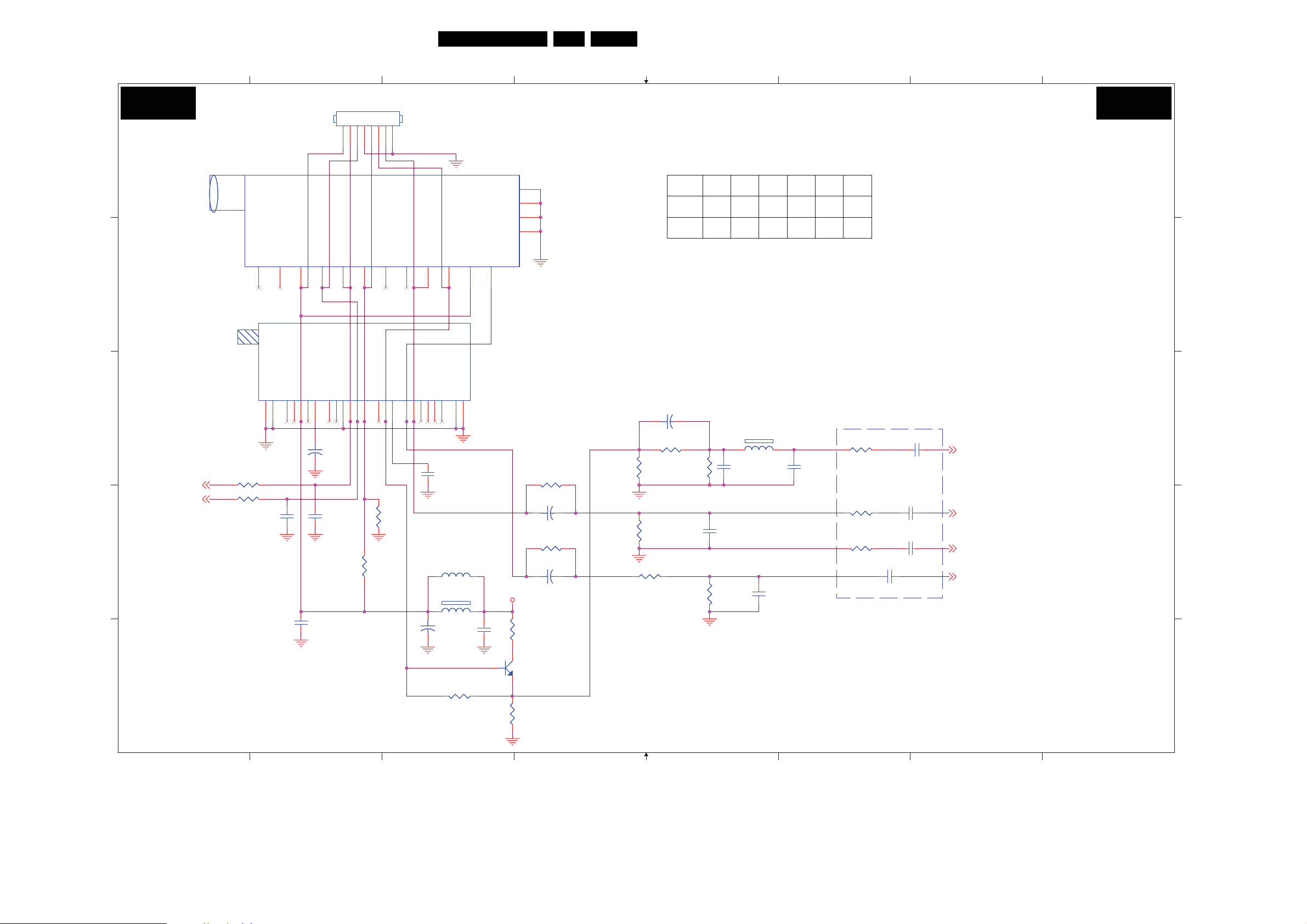
Circuit Diagrams and PWB Layouts
23TPS1.2A LA 7.
WT6702F (Standby MCU)
1
2
3
4
5
6
7
8
WT6702F (STANDBY MCU)
SB09
10K
10K
10K(NC)
10K(NC)
R4127
R4127
R4126
R4126
+3V3_STBY
10K
10K
R4128
R4128
+3V3_STBY
A
33K
33K
6K8
33K
33K
R4131
R4131
R4132
R4132
33K
33K
33K(NC)
33K(NC)
R4124
R4124
R4123
R4123
+3V3_STBY
6K8
R4133
R4133
10K(NC)
10K(NC)
R4125
R4125
10K
10K
33K
33K
R4130
R4130
R4129
R4129
KEY1SB10,12
STA ND B YSB02
5V_PWR_SW
SB01
SB10
SB06,10
SB10,13
SB06,12
RC_IR_3V3
CEC_IRQ
VS_RGB
HS_RGBSB06,10
12V_PWR_SWSB01,10
LED2_STBY
ISP1_SCLSB06,12
ISP1_SDA
I2C_SCLSB03,10,13
I2C_SDASB03,10,13
TXD1SB10,13
RXD1
C4105
C4105
22P
22P
C4106
C4106
100P
100P
10K
10K
R4121
R4121
10K
10K
R4122
R4122
SB10,12
B
SB10,12
C C
FB4101
FB4101
1 2
120R
120R
RESET
R4120
R4120
R4119
R4119
R4118
R4118
R4117
R4117
R4116
R4116
HD_CEC
R4115
R4115
R4114
R4114
R4113
R4113
R4112
R4112
R4111
R4111
R4110
R4110
R4109
R4109
R4108
R4108
R4107
R4107
R4106
R4106
33R
33R
33R
33R
33R
33R
33R
33R
33R
33R
33R
33R
33R
33R
33R
33R
33R
33R
33R(NC)
33R(NC)
33R
33R
22R
22R
22R
22R
33R
33R
33R
33R
+3V3_STBY
R4141
R4141
0R05
0R05
C4101
C4101
10U 10V
10U 10V
4
22
21
20
19
12
11
10
9
8
7
18
17
16
15
14
13
1
A
K
2
D4101
D4101
LS4148(NC)
LS4148(NC)
C4102
C4102
0.1uF
0.1uF
U4101
U4101
NPST
GPIOA0/AD0
GPIOA1/AD1
GPIOA2/AD2
GPIOA3/AD3/IR
GPIOB2/IRQ0
GPIOB3/IRQ1
GPIOB4/VIN
GPIOB5/HIN
GPIOB6/IRQ2/TXD
GPIOB7/IRQ3/RXD
GPIOA4/SCL3
GPIOA5/SDA3
GPIOA6/SCL1
GPIOA7/SDA1
GPIOB0/SCL2
GPIOB1/SDA2
WT6702F_S240
WT6702F_S240
23
VDD
VSS
3
24
32KOSCO
VDD_RTC
32KOSCI
GPIOC1/PWM1
GPIOC0/PWM0
1
2
5
6
R4102
R4102
R4103
R4103
OSCO
OSCI
33R
33R
33R
33R
+3V3_STBY
33K
33K
R4104
R4104
+3V3_SW
OSCO
OSCI
PWR_ON_OFF SB06,10,12
RST_MSPH SB10
33K
33K
R4105
R4105
R4136
R4136
100R(NC)
100R(NC)
R4101
R4101
33R
33R
C4103
C4103
22P
22P
U4102
U4102
1
GND
2
RESET
AP1701FWL(NC)
AP1701FWL(NC)
R4137
R4137
100K(NC)
100K(NC)
1 2
X1401
X1401
32.768KHz
32.768KHz
3
Vcc
+3V3_STBY
+3V3_STBY
C4108
C4108
0.1uF(NC)
0.1uF(NC)
C4104
C4104
22P
22P
SB09
A
B
C4101 A3
C4102 A3
C4103 A6
C4104 A6
C4105 B2
C4106 B2
C4107 D4
C4108 C6
C4109 D5
D4101 C3
FB4101 A3
R4101 A5
R4102 B4
R4103 B4
R4104 B5
R4105 B5
R4106 B3
R4107 B3
R4108 B3
R4109 B3
R4110 B3
R4111 B3
R4112 B3
R4113 B3
R4114 B3
R4115 B3
R4116 B3
R4117 B3
R4118 B3
R4119 A3
R4120 A3
R4121 C2
R4122 C2
R4123 C2
R4124 C2
R4125 C2
R4126 C2
R4127 C2
R4128 C2
R4129 A2
R4130 A2
R4131 A2
R4132 A2
R4133 A2
R4134 C3
R4135 D3
R4136 C5
R4137 C5
R4138 D5
R4139 D6
R4140 D3
R4141 C3
U4101 A3
U4102 C6
X1401 A6
R4140
SB07,10
D D
E E
1
CEC_HDMI
2
CEC_HDMI
R4140
100R
100R
3
R4134 27KR4134 27K
R4135
R4135
0R05
0R05
HD_CEC
C4107
C4107
100P 50V(NC)
100P 50V(NC)
4
RESET
R4138
R4138
5
100R
100R
R4139 10KR4139 10K
+
+
C4109
C4109
4U7 50V
4U7 50V
I_17590_029.eps
6
7
8
260508
Page 24

Circuit Diagrams and PWB Layouts
24TPS1.2A LA 7.
Scaler Board: Scaler MST98980CLD
175
PWM0/MCUCFG0
248
HWRESET
PWM1/MCUCFG1
176
AVDD_AU
AVDD _SIF
70
AVDD_AU
PWM3/MCUCFG3
PWM2/MCUCFG2
192
191
R4205
R4205
C4237
C4237
0.1uF
0.1uF
63
5
100R
100R
RST_MSPH SB09
VDDP
VDDC
AVDDA
101
149
185
193
AVDD_33
SCK
58
168
AVDD_33
SDI
169
R4236
R4236
15K(NC)
15K(NC)
SCZ
VDDC
SDO
170
240
165
VDDP99VDDP
VDDC
VDDC
VDDC
VDDC
MST98980CLD-LF
MST98980CLD-LF
GND
GND
GND
3
11
17
40
SPI_DO SB11
SPI_CZ SB11
SPI_DI SB11
SPI_CK SB11
RC_IR_3V3 SB09,12
VDDP
GND
183
61
SB18
194
GND
66
14
39
254
AVDD_33
AVDD_33
AVDD_SIF
IRIN
167
182
+3V3_SW
R4235
R4235
100R
100R
VDDP
GND
207
VDDP
GND
100
221
235
VDDP
VDDP
U4201
U4201
GND
GND
GND
105
113
134
DRV_USB
AVDD_MemPLL
VDDM
108
114
119
VDDM
VDDM
GND
GND
166
184
148
6
135
147
VDDM
VDDM
VDDM
GND
GND
GND
208
222
+3V3_STBY
AVDD_MPLL
136
AVDD_MEMPLL
GND
TH1
241
257
R4237
R4237
33K
33K
7
R4288
R4288
47R(NC)
47R(NC)
R4289
47R
R4289
47R
R4290
47R
R4290
47R
R4307
R4307
47R(NC)
47R(NC)
47R
47R
R4291
R4291
R4292
47R
R4292
47R
+3V3_SW
97
96
98
251
GPIOF[9]
GPIOF[8]
AVDD _MP LL
GPIOB[6]
AD[1]
AD[2]
AD[3]
AD[0]
186
155
156
158
154
157
AD[5]
AD[6]
AD[4]
159
160
187
GPIOF[0]89GPIOF[1]90GPIOF[2]91GPIOF[3]92GPIOF[4]93GPIOF[5]94GPIOF[6]95GPIOF[7]
LVSYNC/GPIOE[0]
LVH SYNC/GPIOE[1]
LDE/GPIOE[2]
LCK/GPIOE[3]
LVB4M/NC
MDATA[10]
MDATA[11]
MDATA[12]
MDATA[13]
MDATA[14]
MDATA[15]
AD[7]
ALE
RDZ
WRZ
R4248
R4248
161
164
163
162
R4247
R4247
R4246
R4246
R4245
R4245
R4244
R4244
R4243
R4243
R4242
R4242
R4241
R4241
R4240
R4240
R4239
R4239
R4238
R4238
189
188
OTG_DP
OTG_DM
OTG_VBUS
DI[13]
DI[12]
DI[11]
DI[10]
IVSYNC
IHSYNC
ICLK
LVB 0M
LVB 0P
LVB 1M
LVB 1P
LVB 2M
LVB 2P
LVB CK M
LVB CK P
LVB 3M
LVB 3P
LVB 4P / NC
LVA0 M
LVA0 P
LVA1 M
LVA1 P
LVA2 M
LVA2 P
LVAC KM
LVAC KP
LVA3M
LVA3P
LA4M/NC
LVA4P/NC
MDATA[0]
MDATA[1]
MDATA[2]
MDATA[3]
MDATA[4]
MDATA[5]
MDATA[6]
MDATA[7]
MDATA[8]
MDATA[9]
MCLK
MCLKE
UDQM
LDQM
RASZ
CASZ
WEZ
BARD[1]
BARD[0]
MADR[11]
MADR[10]
MADR[9]
MADR[8]
MADR[7]
MADR[6]
MADR[5]
MADR[4]
MADR[3]
MADR[2]
MADR[1]
MADR[0]
190
DI[9]
DI[8]
DI[7]
DI[6]
DI[5]
DI[4]
DI[3]
DI[2]
DI[1]
DI[0]
IDE
181
OTG_CID
NC
NC
NC
NC
47R
47R
47R
47R
47R
47R
47R
47R
47R
47R
47R
47R
47R
47R
47R
47R
56R
56R
47R
47R
47R(NC)
47R(NC)
INT
247
246
245
244
243
242
239
238
237
236
234
233
232
231
230
229
228
227
226
225
224
223
220
219
218
217
216
215
214
213
212
211
210
209
206
205
204
203
202
201
200
199
198
197
196
195
123
122
121
120
118
117
116
115
112
111
110
109
107
106
104
103
130
129
128
127
126
125
124
102
133
137
138
131
132
153
152
151
150
146
145
144
143
142
141
140
139
10K(NC)
10K(NC)
R4249
R4249
+3V3_SW
R4273
R4273
R4272
R4272
R4271
R4271
R4270
R4270
R4269
R4269
R4268
R4268
R4267
R4267
R4266
R4266
R4265
R4265
R4264
R4264
R4263
R4263
R4310
R4310
R4312
R4312
TP4211TP4211
R4262
R4262
R4261
R4261
R4260
R4260
TP4210TP4210
MDATA0
MDATA1
MDATA2
MDATA3
MDATA4
MDATA5
MDATA6
MDATA7
MDATA8
MDATA9
MDATA10
MDATA11
MDATA12
MDATA13
MDATA14
MDATA15
MCLK
MCLKZ
CKE
MVREF
UDQM
LDQM
DQS0
DQS1
RASZ
CASZ
WEZ
BA1
BA0
MADR11MADR11
MADR10
MADR9
MADR8
MADR7
MADR6
MADR5
MADR4
MADR3
MADR2
MADR1
MADR0
10K
10K
10K
10K
R4252
R4252
R4251
R4251
10K(NC)
10K(NC)
R4255
R4255
10K
10K
R4256
R4256
47R
47R
47R
47R
47R
47R
47R
47R
47R
47R
47R
47R
47R
47R
47R
47R
47R
47R
47R
47R
47R
47R
47R
47R
47R
47R
47R
47R
47R
47R
47R
47R
10K(NC)
10K(NC)
R4257
R4257
10K
10K
10K(NC)
10K(NC)
R4258
R4258
R4259
R4259
10K
10K
10K(NC)
10K(NC)
R4274
R4274
R4275
R4275
RXO0- SB14
RXO0+ SB14
RXO1- SB14
RXO1+ SB14
RXO2-
RXO2+ SB14
RXOC- SB14
RXOC+ SB14
RXO3- SB14
RXO3+ SB14
RXE0- SB14
RXE0+ SB14
RXE1- SB14
RXE1+ SB14
RXE2- SB14
RXE2+ SB14
RXEC- SB14
RXEC+ SB14
RXE3- SB14
RXE3+ SB14
NVRAM_WP
33K
33K
R4309
R4309
+3V3_STBY
10K
10K
R4277
R4277
33K(NC)
33K(NC)
R4250
R4250
10K
10K
10K
10K
10K
10K
R4279
R4279
R4280
R4280
R4278
R4278
33K
33K
33K
33K
R4254
R4254
R4253
R4253
8
OTG_VBUS SB18
OTG_DM SB18
OTG_DP SB18
OTG_CID SB18
+3V3_STBY
10K
10K
10K
10K
33K
33K
10K
10K
10K
10K
10K
10K
10K(NC)
10K(NC)
10K(NC)
10K(NC)
R4285
R4285
R4286
R4286
R4281
R4281
R4282
R4282
R4313
R4313
R4287
R4287
R4283
R4283
R4284
R4284
SB14
MDATA[0..15]
MADR[0..11]
DDC_WP SB07
CEC_IRQ SB09
CEC_HDMI SB07,09
PWR_ON_OFF SB06,09,12
5V_PWR_SW1 SB01
12V_PWR_SW SB01,09
2ND_CZ SB11
LED1_ON SB12
LED2_STBY SB09,12
33K
33K
33K
33K
33K
33K
R4276
R4276
R4308
R4308
R4311
R4311
PANEL_PWR SB01
BL_EN SB02
12V_PWR_SW1 SB16
AMP_STBY_CTRL SB16
AMP_MUTE_CTRL SB16
AMP_GAIN0 SB16
AMP_GAIN1 SB16
HP_STBY SB16
HP_DET SB05
OD_SEL SB14
MM_DVBT_PWR SB13
TXD1 SB09,13
RXD1 SB09,13
OTG_OC_DET SB18
MDATA[0..15] SB11
MCLK SB11
MCLKZ SB11
CKE SB11
UDQM SB11
LDQM SB11
DQS0 SB11
DQS1 SB11
RASZ SB11
CASZ SB11
WEZ SB11
BA1 SB11
BA0 SB11
MADR[0..11] SB11
9
POWER ON RESET
MSPH_RST
100R(NC)
100R(NC)
ISP & Debug PORT
RXD
TXD
NVRAM
U4203
U4203
1
A0
VCC
2
A1
WP
3
SCL
A2
4
GND
SDA
M24C32-WMN6TP
M24C32-WMN6TP
U4205
U4205
1
8
VCC
E0
2
7
WC
E1
3
6
E2
SCL
5
VSS4SDA
M24C32WBN6P PDIP8(NC)
M24C32WBN6P PDIP8(NC)
R4293
R4293
+5V_STBY
I2C address
at A0
C4254
C4254
0.1uF
0.1uF
8
7
6
5
VDDP
R4296
R4296
R4297
R4297
C4210
C4210
100N
100N
C4230
C4230
0.1uF
0.1uF
C4203
C4203
0.1uF
0.1uF
C4219
C4219
100N
100N
C4211
C4211
0.1uF
0.1uF
C4231
C4231
0.1uF
0.1uF
2
AVDDA
C4205
C4205
C4204
C4204
100N
100N
0.1uF
0.1uF
C4212
C4212
100N
100N
C4220
C4220
0.1uF
0.1uF
C4232
C4232
0.1uF
0.1uF
KEY1SB09,12
C4221
C4221
100N
100N
R4306
R4306
C4213
C4213
100N
100N
C4233
C4233
0.1uF
0.1uF
VDDM
SB13
+3V3_SW
0R(NC)
0R(NC)
C4214
C4214
100N
100N
MM_DVBT_SW
Q4201
Q4201
2N7002
2N7002
C4248
C4248
4.7uF
4.7uF
SB06
PANEL_IDSB02
BL_ADJSB02
SPI_WPSB11
KEY1#
C4215
C4215
0.1uF
0.1uF
VDDP
R4210
R4210
R4211
R4211
C4249
C4249
1uF
1uF
R42120RR4212
I2C_SDASB03,09,13
I2C_SCLSB03,09,13
ISP2_SDA
ISP2_SCLSB06
KEY2SB12
3
AVDDA
BAS32L(NC)
BAS32L(NC)
R4207
R4207
390R 1%
390R 1%
C4241
C4241
C4242 100NC4242 100N
47R
47R
47R
47R
C4250
C4250
0.1uF
0.1uF
0R
KEY1#
+3V3_SW
2
D4201
D4201
1
100N
100N
C4246 47NC4246 47N
C4247 47NC4247 47N
+
+
C4251
C4251
10uF 50V
10uF 50V
C4252 0.1uFC4252 0.1uF
I2C_SDA
I2C_SCL
TXD
RXD
6K8
6K8
10K
10K
3K3
3K3
10K
10K
R4222
R4222
R4223
R4223
R4221
R4221
R4224
R4224
R4305
R4305
C4256
C4256
0.1uF
0.1uF
K
A
10K(NC)
10K(NC)
R4225
R4225
VDDP
10K
10K
10K(NC)
10K(NC)
R4226
R4226
+
+
C4236
C4236
10uF 50V(NC)
10uF 50V(NC)
R4203
R4203
10K(NC)
10K(NC)
SB07
SB07
SB07
SB08
SB08
SB08
SB08
SB08
SB08
SB08
SB08
C4243
C4243
0.1uF(NC)
0.1uF(NC)
R4208
R4208
R4209
R4209
SB04
SB06
SB06
SB06
SB04
SB04
SB05
B04
TUNER_CVBSSB03
SB03
SB15
SB15
SB15
SB16
TXCLK1TXCLK1+SB07
B_1TX0-SB07
B_1TX0+
G_1TX1-SB07
G_1TX1+
R_1TX2-SB07
R_1TX2+SB07
SDA_HD1SB07
SCL_HD1SB07
TXCLK2TXCLK2+
B_2TX0B_2TX0+SB08
G_2TX1G_2TX1+
R_2TX2R_2TX2+SB08
SDA_HD2SB08
SCL_HD2
HS_RGBSB06,09
VS_RGBSB06,09
AV_CVBS1S
AV_CVBS0SB05
CVBSOutSB13
AUMONOSB03
ITV_AUOutLSB13
ITV_AUOutRSB13
LineoutLSB17
LineoutRSB17
AUOutLSB16
AUOutR
R4227
R4227
10K
10K
R4231
R4231
10K(NC)
10K(NC)
R4204
R4204
HPD1SB07
HPD2
47R
47R
47R
47R
SV_C0
SV_Y0SB05
R4213
R4213
R4214
R4214
R4215
R4215
R4216
R4216
R42171KR4217
R42181KR4218
R42191KR4219
R42201KR4220
+3V3_SW
C4238
C4238
C4239
C4239
C4240
C4240
C4244 47NC4244 47N
C4245
C4245
PB1+SB04
Y1+SB04
SOY1
PR1+SB04
BIN+
SOG
GIN+SB06
RIN+
PB2+
SOY2SB04
Y2+
PR2+SB04
SIFP0
SIFM0SB03
AUL0SB15
AUR0SB15
AUL1SB15
AUR1SB15
AUL2
AUR2
AUL3SB15
AUR3
27P
27P
27P
27P
R4228
R4228
10K(NC)
10K(NC)
R4232
R4232
10K
10K
4
100R(NC)
100R(NC)
47N
47N
TP4214TP4214
TP4201TP4201
TP4202TP4202
TP4204TP4204
TP4205TP4205
TP4208TP4208
TP4209TP4209
47R
47R
47R
47R
22R
22R
22R
22R
1K
1K
1K
1K
12
0.1uF
0.1uF
X4201
X4201
14.318MHZ
14.318MHZ
9
10
12
13
15
16
18
19
20
21
22
23
252
253
255
256
1
2
4
5
6
7
8
26
27
28
33
35
34
36
37
38
41
42
24
25
29
30
31
32
43
44
45
46
47
48
49
50
51
52
53
54
55
56
57
59
60
62
64
65
69
68
67
71
72
73
74
75
76
77
78
79
80
81
82
83
84
85
86
87
88
177
178
179
180
171
172
173
174
R4229
R4229
10K(NC)
10K(NC)
R4233
R4233
10K
10K
MSPH_RST
R4206
R4206
1M(NC)
1M(NC)
RXACKN
RXACKP
RXA0N
RXA0P
RXA1N
RXA1P
RXA2N
RXA2P
HPLUGA
REXT
DDCDA_DA
DDCDA_CK
RXBCKN
RXBCKP
RXB0N
RXB0P
RXB1N
RXB1P
RXB2N
RXB2P
HPLUGB
DDCDB_DA
DDCDB_CK
VCLAMP
REFP
REFM
VCOM3
VCOM2
BIN0P
GIN0P
SOGIN0
RIN0P
HSYNC0
VSYNC0
HSYNC1
VSYNC1
BIN1P
SOGIN1
GIN1P
RIN1P
VSYNC2
BIN2P
SOGIN2
GIN2P
RIN2P
C1
Y1
C0
Y0
CVBS3
CVBS2
CVBS1
VCOM1
CVBS0
VCOM0
CVBSOUT1
CVBSOUT0
SIF0P
SIF1P
SIFM
AUVREF
AUVRADP
AUVRADN
AUL0
AUR0
AUL1
AUR1
AUCOM
AUL2
AUR2
AUL3
AUR3
AUMONO
AUOUTL3
AUOUTR3
AUOUTL2
AUOUTR2
AUOUTL1
AUOUTR1
AUOUTL0
AUOUTR0
DDCR_DA
DDCR_CK
DDCA_DA
DDCA_CK
SAR0
SAR1
SAR2
SAR3
R4230
R4230
10K
10K
R4234
R4234
10K(NC)
10K(NC)
250
PWM0
PWM1
PWM2
PWM3
249
XIN
XOUT
1
SB10
A
FB4201
FB4201
1 2
+3V3_SW
+3V3_SW
B B
+3V3_SW
C C
+1V2 VDDC
D
E E
F F
+2V6
+3V3
G G
H H
+3V3
120R
120R
FB4202
FB4202
1 2
120R
120R
FB4203
FB4203
1
120R
120R
+1.2V for VDDC
FB4204
FB4204
1
120R
120R
FB4205
FB4205
1 2
120R
120R
FB4206
FB4206
1 2
120R
120R
FB4207
FB4207
1
120R
120R
FB4208
FB4208
1 2
120R(NC)
120R(NC)
FB4209
FB4209
1 2
120R
120R
C42341NC4234
1N
SCALER MST98980CLD
+3.3VSW for AVDDA
Pin14, Pin254, Pin39, Pin58
C4201
C4201
C4202
C4202
10U 10V
10U 10V
100N
100N
+3.3VSW for AVDD_MPLL
Pin251
AVDD_MPLL
C4206
C4206
C4207
C4207
10U 10V
10U 10V
0.1uF
0.1uF
+3.3VSW for VDDP
Pin99, Pin165, Pin183, Pin194, Pin207, Pin221, Pin235
2
C4208
C4208
C4209
C4209
100N
100N
10U 10V
10U 10V
Pin101, Pin149, Pin185, Pin193, Pin240
2
C4216
C4216
C4217
C4217
C4218
C4218
100N
10U 10V
10U 10V
+3.3V for AVDD_SIF
C4222
C4222
10U 10V
10U 10V
+3.3V for AVDD_AU
C4224
C4224
10U 10V
10U 10V
+3.3V for AVDD_MemPLL
2
C4226
C4226
10U 10V
10U 10V
+2.6V/3.3V for VDDM
C4228
C4228
10U 10V
10U 10V
VDDM
R4201
R4201
10K
10K
R4202
R4202
C4235
C4235
0.1uF
0.1uF
10K
10K
100N
100N
100N
Pin63
AVDD_SIF+3V3
C4223
C4223
0.1uF
0.1uF
Pin70
AVDD_AU+3V3
C4225
C4225
0.1uF
0.1uF
Pin251
AVDD_MemPLL
C4227
C4227
100N
100N
Pin108, Pin114, Pin119, Pin135, Pin147
C4229
C4229
0.1uF
0.1uF
MVREF
R4294
R4294
4K7(NC)
4K7(NC)
R4295
R4295
100K(NC)
100K(NC)
+3V3_SW
10
1
GND
2
RESET
AP1702EWL(NC)
AP1702EWL(NC)
10R
10R
10R
10R
63384 4P 2.0MM
63384 4P 2.0MM
R4298
R4298
10K
10K
U4202
U4202
1
2
3
4
VCC
CN4201
CN4201
R4299
R4299
10K(NC)
10K(NC)
11
SB10
VDDP
3
C4253
C4253
0.1uF(NC)
0.1uF(NC)
R4300
R4300
10K(NC)
10K(NC)
NVRAM_WP
I2C_SCL
I2C_SDA
CN4201 C10 C4201 A1
C4202 A1 C4203 A2
C4204 A2 C4205 A2
C4206 B1 C4207 B1
C4208 C1 C4209 C1
C4210 C2 C4211 C2
C4212 C2 C4213 C2
C4214 C2 C4215 C3
C4216 C1 C4217 C1
C4218 C2 C4219 C2
A
C4220 C2 C4221 C2
C4222 D1 C4223 D1
C4224 E1 C4225 E1
C4226 F1 C4227 F1
C4228 F1 C4229 F1
C4230 F2 C4231 F2
C4232 F2 C4233 F2
C4234 G1 C4235 G1
C4236 A3 C4237 A5
C4238 A4 C4239 B4
C4240 C4 C4241 C3
C4242 C3 C4243 C3
C4244 C4 C4245 C4
C4246 E3 C4247 E3
C4248 E3 C4249 E3
C4250 E3 C4251 E3
C4252 E3 C4253 B10
C4254 D10 C4256 G3
D4201 A3 FB4201 A1
FB4202 B1 FB4203 C1
FB4204 C1 FB4205 D1
FB4206 E1 FB4207 E1
FB4208 F1 FB4209 F1
Q4201 H2 R4201 G1
R4202 G1 R4203 A3
R4204 A4 R4205 A5
R4206 A4 R4207 B3
C4 R4209 C4
R4208
R4210 E3 R4211 E3
R4212 E3 R4213 F4
R4214 F4 R4215 F4
R4216 F4 R4217 F4
R4218 F4 R4219 F4
R4220 F4 R4221 G3
R4222 G3 R4223 G3
R4224 G3 R4225 G3
R4226 G3 R4227 G4
R4228 G4 R4229 G4
R4230 G4 R4231 G4
R4232 G4 R4233 G4
R4234 G4 R4235 G5
R4236 G5 R4237 G6
R4238 G7 R4239 G7
R4240 G7 R4241 G7
R4242 G7 R4243 G7
R4244 G7 R4245 G7
R4246 G7 R4247 G7
R4248 G7 R4249 G7
R4250 G8 R4251 G7
R4252 G7 R4253 G8
R4254 G8 R4255 G7
R4256 G7 R4257 G7
R4258 G7 R4259 G8
R4260 C7 R4261 C7
R4262 C7 R4263 C7
R4264 B7 R4265 B7
R4266 B7 R4267 B7
R4268 B7 R4269 B7
R4270 B7 R4271 B7
R4272 B7 R4273 B7
D
R4274 B8 R4275 B8
R4276 B8 R4277 B8
R4278
B8 R4279 B8
R4280 B8 R4281 B8
R4282 B8 R4283 B8
R4284 B8 R4285 B8
R4286 B8 R4287 B8
R4288 A7 R4289 A7
R4290 A7 R4291 A7
R4292 A7 R4293 B9
R4294 A10 R4295 B10
R4296 C10 R4297 C10
R4298 D10 R4299 D10
R4300 D10 R4305 G3
R4306 H2 R4307 A7
R4308 B8 R4309 G8
R4310 C7 R4311 B8
R4312 C7 R4313 B8
TP4201 D4 TP4202 D4
TP4204 E4 TP4205 E4
TP4208 F4 TP4209 F4
TP4210 C7 TP4211 C7
TP4214 D4 U4201 B4
U4202 A10 U4203 D9
U4205 E9 X4201 A4
I_17590_030.eps
1
2
3
4
5
6
7
8
9
10
260508
11
Page 25

Circuit Diagrams and PWB Layouts
25TPS1.2A LA 7.
Scaler Board: Flash ROM & Memory
1
2
3
4
5
6
7
8
9
10
11
FLASH ROM & MEMORY
SB11
C4406
C4406
0.1uF
0.1uF
DMC
DMQ
C4407
C4407
C4408
C4408
0.1uF
0.1uF
0.1uF
0.1uF
47R
47R
47R
47R
47R
47R
ADR0
ADR1
ADR2
ADR3
ADR4
ADR5
ADR6
ADR7
ADR8
ADR9
ADR10
ADR11
WEZM
CASZM
RASZM
DQMS0
DQMS1
5
6
7
8
5
6
7
8
5
6
7
8
29
30
31
32
35
36
37
38
39
40
28
41
21
22
23
16
51
20
47
26
27
24
14
17
34
48
66
12
52
58
64
+2V6
R4403
R4403
10K
10K
MVREF-D
C4409
C4409
0.1uF
0.1uF
U4401
U4401
A0
A1
A2
A3
A4
A5
A6
A7
A8
A9
A10/AP
A11
WE
CAS
RAS
LDQS
UDQS
LDM
UDM
BA0
BA1
CS
NC
NC
VSS
VSS
VSS
6
VSSQ
VSSQ
VSSQ
VSSQ
VSSQ
HY5DU281622FTP-5(NC)
HY5DU281622FTP-5(NC)
R4404
R4404
10K
10K
DQ0
DQ1
DQ2
DQ3
DQ4
DQ5
DQ6
DQ7
DQ8
DQ9
DQ10
DQ11
DQ12
DQ13
DQ14
DQ15
VREF
CLK
CLK
CKE
MVDD
MVDD
MVDD
VDDQ
VDDQ
VDDQ
VDDQ
VDDQ
NC
NC
NC
NC
NC
NC
C4410
C4410
0.1uF
0.1uF
C44111NC4411
1N
MDATA8
47R
DATA8
RP4401
2
4
5
7
8
10
11
13
54
56
57
59
60
62
63
65
49
46
45
44
19
25
42
43
50
53
1
18
33
3
9
15
55
61
RP4401
DATA9
DATA10
DATA11
DATA12
DATA13
DATA14
DATA15
RP4402
RP4402
DATA0
RP4403
RP4403
DATA1
DATA2
DATA3
DATA4
DATA5
DATA6
DATA7
RP4404
RP4404
MVREF-D
MCLKMCLK+
CKE
256M
R4413 22R(NC)R4413 22R(NC)
DMC
DMQ
4
3
2
1
4
3
2
1
4
3
2
1
4
3
2
1
R4412 150R 1%(NC)R4412 150R 1%(NC)
CKE SB10
47R
5
6
7
8
5
6
7
8
5
6
7
8
5
6
7
8
47R
47R
47R
47R
47R
47R
MDATA9
MDATA10
MDATA11
MDATA12
MDATA13
MDATA14
MDATA15
MDATA0
MDATA1
MDATA2
MDATA3
MDATA4
MDATA5
MDATA6
MDATA7
MDATA[0..15]
MDATA[0..15] SB10
BA0SB10
SB10
BA1
R4414
R4414
4K7
4K7
DMC
R4415
R4415
4K7
4K7
DQMS0
DQMS1
BA0
BA1
ADR0
ADR1
ADR2
ADR3
ADR4
ADR5
ADR6
ADR7
ADR8
ADR9
ADR10
ADR11
RASZM
CASZM
WEZM
MCLK+
U4402
U4402
23
A0
24
A1
25
A2
26
A3
29
A4
30
A5
31
A6
32
A7
33
A8
34
A9
22
A10
35
A11
18
RAS
17
CAS
16
WE
38
CLK
19
CS
15
LDQM
39
UDQM
20
BA0/A13
21
BA1/A12
28
VSS
41
VSS
54
VSS
6
VSSQ
12
VSSQ
46
VSSQ
52
VSSQ
HY57V641620FTP-6-C
HY57V641620FTP-6-C
D10
D11
D12
D13
D14
D15
CKE
VDD
VDD
VDD
VDDQ
VDDQ
VDDQ
VDDQ
D0
D1
D2
D3
D4
D5
D6
D7
D8
D9
NC
NC
DATA9
4
DATA10
5
DATA11
7
DATA12
8
DATA13
10
DATA14
11
DATA15
13
DATA0
42
DATA1
44
DATA2
45
DATA3
47
DATA4
48
DATA5
50
DATA6
51
DATA7
53
CKE
37
36
DMC
40
1
14
27
3
9
43
49
DMQ
DATA8
2
SDRAM 4M x 16
DDR 2M x 16bit x 4BK
FB4401
FB4401
R4401
0R(NC)
R4401
R44020RR4402
DMC
0R(NC)
0R
C4402
C4402
0.1uF
0.1uF
MADR[0..11]MADR[0..11]
SB10
SB10
SB10
SB10
C4403
C4403
0.1uF
0.1uF
UDQMSB10
LDQMSB10
MCLKSB10
MCLKZSB10
WEZSB10
CASZ
RASZ
DQS1
DQS0SB10
BA0
BA1SB10
C4401
C4401
10U 10V
10U 10V
C4404
C4404
0.1uF
0.1uF
MADR0
MADR1
MADR2
MADR3
MADR4
MADR5
MADR6
MADR7
MADR8
MADR9
MADR10
MADR11
WEZ
CASZ
RASZ
DQS1
DQS0
UDQM
LDQM
BA0
BA1
MCLK+
MCLK-
+2V6
A
B
C C
D D
E
+3V3
MADR[0..11]SB10
1 2
FB4402
FB4402
1 2
DMQ
C4405
C4405
0.1uF
0.1uF
RP4405
RP4405
4
3
2
1
4
3
2
1
RP4406
RP4406
4
3
2
1
RP4407
RP4407
R4405 22RR4405 22R
R4406 22RR4406 22R
R4407 22RR4407 22R
R4408 56R(NC)R4408 56R(NC)
R4409 56R(NC)R4409 56R(NC)
R4410 56RR4410 56R
R4411 56RR4411 56R
120R
120R
120R
120R
SB11
C4401 A2 C4402 B1
C4403 B1 C4404 B2
C4405 B2 C4406 B2
C4407 B3 C4408 B3
C4409 B3 C4410 B4
C4411 B5 C4412 F4
C4413 F9 FB4401 A2
FB4402 A2 RP4401 B5
RP4402 C5 RP4403 C5
RP4404 C5 RP4405 B2
RP4406 C2 RP4407 C2
R4401 A1 R4402 A1
R4403 A4 R4404 B4
R4405 C2 R4406 C2
R4407 C2 R4408 C2
R4409 D2 R4410 D2
R4411 D2 R4412 D5
R4413 D5 R4414 D7
R4415 D8 R4416 G3
R4417 G3 R4418 G3
R4419 G5 R4420 G5
R4421 F8 R4422 G8
R4423 F3 R4424 G5
U4401 B4 U4402 C9
U4403 G3 U4404 G8
A
B
E
F F
SB10
G G
H H
1
1st SPI Flash ROM for Main Control
+3V3_SW
R4423
R4423
10K
SPI_CZSB10
SPI_DOSB10
SPI_WP
2
R4416
R4416
R4417
R4417
R4418
R4418
82R
82R
82R
82R
0R(NC)
0R(NC)
10K
SPI_FDO
3
U4403
U4403
1
VCC
CS#
2
SO
HOLD#
3
W#
SCK
4
GND
MX25L4005AM2C-12G
MX25L4005AM2C-12G
SI
+3V3_SW
8
7
6
5
4
C4412
C4412
0.1uF
0.1uF
SPI_FCK
SPI_FDI
R4419
R4419
R4420
R4420
82R
82R
82R
82R
R44240RR4424
5
0R
SPI_CK SB10
SPI_DI SB10
6
7
2nd SPI Flash ROM for USB
+3V3_SW
R4421
R4421
10K(NC)
10K(NC)
2ND_CZSB10
SPI_FDO
10K(NC)
10K(NC)
8
R4422
R4422
U4404
U4404
1
CS#
2
SO
3
W#
4
GND
MX25L8005M2I-15G(NC)
MX25L8005M2I-15G(NC)
VCC
HOLD#
SCK
SI
+3V3_SW
8
7
6
5
9
C4413
C4413
0.1uF(NC)
0.1uF(NC)
SPI_FCK
SPI_FDI
I_17590_031.eps
10
260508
11
Page 26

Circuit Diagrams and PWB Layouts
26TPS1.2A LA 7.
Scaler Board: KEY, IR BD & Compair I/F
1
2
3
4
5
6
7
8
KEY, IR BD, & COMPAIR I/F
SB12
For Key BOARD For Compair I/F
ZD7301
ZD7301
BZX84-C5V6 (NC)
BZX84-C5V6 (NC)
1 3
PWR_ON_OFF_IN
BZX84-C5V6 (NC)
BZX84-C5V6 (NC)
C7302
C7302
0.1uF
0.1uF
IR IN/OUT I/F for MM/DVB-T Module/ Serial Plug (ITV Level 2)
A A
B
KEY1SB09,10
SB10
KEY2
ZD7302
ZD7302
1 3
For IR BOARD
R7310
R7310
R7301
R7301
R7302
R7302
C7301
C7301
0.1uF
0.1uF
+5V_STBY
0R05
0R05
4R7
4R7
4R7
4R7
R73030RR7303
0R
1
2
3
4
CN7301
CN7301
63364 4P 2.0mm
63364 4P 2.0mm
+5V_STBY
SB06
ISP_SDASB06
ISP_SCL
R7308
R7308
R7309
R7309
22R
22R
22R
22R
1
2
3
CN7303
CN7303
63383 3P 2.0mm (H=15mm)
ZD7304
ZD7304
ZD7303
ZD7303
1 3
1 3
BZX84-C5V6(NC)
BZX84-C5V6(NC)
63383 3P 2.0mm (H=15mm)
BZX84-C5V6(NC)
BZX84-C5V6(NC)
SB12
B
CN7301 A3
CN7302 C5
CN7303 A6
CN7304 C4
CN7305 C5
C7301 A2
C7302 A2
C7303 D2
C7304 B4
C7305 D4
FB7301 D4
Q7301 C2
Q7302 C2
R7301 A2
R7302 A2
R7303 A3
R7304 D3
R7305 D3
R7306 D3
R7307 D3
R7308 A5
R7309 A5
R7310 A2
R7311 C3
R7312 C4
R7313 C4
R7314 C3
R73
15 C4
R7316 B2
U7301 B3
ZD7301 A2
ZD7302 A1
ZD7303 A5
ZD7304 A5
R7313
R7313
47R(NC)
47R(NC)
120R
120R
+5V_STBY
R7315
R7315
47K(NC)
47K(NC)
IR_MODE
2
1
CN7304
CN7304
63362 2P 2.0MM(NC)
63362 2P 2.0MM(NC)
+5V_STBY
C7305
C7305
0.1uF
0.1uF
3
2
1
CN7305
CN7305
63363 3P 2.0mm(NC)
63363 3P 2.0mm(NC)
1
2
3
4
5
6
7
CN7302
CN7302
63367 7P 2.0MM
63367 7P 2.0MM
R7316
R7316
47K(NC)
47K(NC)
2
Q7302
Q7302
MUN2211J(NC)
MUN2211J(NC)
C C
+5V_STBY
Q7301
Q7301
2N7002
2N7002
SB09,10
RC_IR_3V3
LED2_STBYSB09,10
LED1_ONSB10
SB06,09,10
D D
PWR_ON_OFF
C7303
C7303
33P
33P
1 3
RC_IR_5V SB13
74LV4053PW(NC)
74LV4053PW(NC)
R7314
R7314
47R(NC)
47R(NC)
R7311
R7311
R7304
R7304
R7305
R7305
R7306
R7306
R7307
R7307
U7301
U7301
11
10
47R(NC)
47R(NC)
47R
47R
100R
100R
100R
100R
100R
100R
9
6
16
14
1Z
VCC
S1
1Y0
S2
1Y1
S3
2Y0
2Y1
3Y0
E
3Y1
2Z153Z4GND8VEE
PWR_ON_OFF_IN
C7304
C7304
0.1uF(NC)
0.1uF(NC)
12
13
2
1
R7312
R7312
5
47R(NC)
47R(NC)
3
7
1 2
FB7301
FB7301
E
I_17590_032.eps
1
2
3
4
5
6
7
8
E
260508
Page 27

Scaler Board: ITV I/F
1
Circuit Diagrams and PWB Layouts
2
27TPS1.2A LA 7.
3
4
5
6
7
8
ITV I/F
CN7402
SB13
Power for MM/DVB-T Module/ I-BOARD (ITV Level 2)
FB7403
FB7403
A A
+
+
C7414
C7414
10uF 50V(NC)
CN7401
1
2
3
4
5
CN7401
63172 3P 2.5mm(NC)
63172 3P 2.5mm(NC)
1
2
3
47R(NC)
R7415
R7415
R7416
R7416
47R(NC)
47R(NC)
47R(NC)
CN7406
CN7406
64835 5P 2.5mm(NC)
64835 5P 2.5mm(NC)
B B
10uF 50V(NC)
+
+
C7401
C7401
470uF 25V(NC)
470uF 25V(NC)
MM_DVBT_PWR SB10
MM_DVBT_SW SB10
1 2
120R(NC)
120R(NC)
C7415
C7415
0.1uF(NC)
0.1uF(NC)
FB7401
FB7401
1 2
120R(NC)
120R(NC)
C7402
C7402
0.1uF(NC)
0.1uF(NC)
Module
DVB-T/I-Board
MM
C7416
C7416
0.1uF(NC)
0.1uF(NC)
C7403
C7403
0.1uF(NC)
0.1uF(NC)
+12V_SW
+5V_STBY
C7401
as shown
220uF 25V
CN7402
1
2
3
4
5
63385 5P 2.0mm(NC)
63385 5P 2.0mm(NC)
+5V_STBY
SB10
1 2
CVBSOut
CVBS_TERR_OUT
FB7402
FB7402
600R(NC)
600R(NC)
+5V_STBY
C7406
C7406
0.1uF(NC)
0.1uF(NC)
R7407
R7407
C7405
C7405
LCD CLOCK I/F (ITV Level 2)
I-BOARD SYSTEM I/F (ITV Level 2)
I2C_SCL SB03,09,10
I2C_SDA SB03,09,10
+
+
10uF(NC)
10uF(NC)
C7409
C7409
47P 50V(NC)
47P 50V(NC)
C7407
C7407
10U 10V(NC)
10U 10V(NC)
0R(NC)
0R(NC)
R7414
R7414
C7408 47uF 25V(NC)
C7408 47uF 25V(NC)
R7410
R7410
R7408
R7408
10K(NC)
10K(NC)
R7409
R7409
10K(NC)
10K(NC)
+
+
470R(NC)
470R(NC)
2
0R(NC)
0R(NC)
1
2
3
3
Q7402
Q7402
BC847C(NC)
BC847C(NC)
1
BC858CG(NC)
BC858CG(NC)
Q7403
Q7403
R7413
R7413
75R(NC)
75R(NC)
R7412
R7412
75R(NC)
75R(NC)
R7411
R7411
75R(NC)
75R(NC)
SB13
CN7401 A1 CN7402 A4
CN7403 C2 CN7404 D7
CN7406 A1 CN7407 D7
CN7408 D3 C7401 A2
C7402 B2 C7403 B3
C7404 D5 C7405 B5
C7406 B5 C7407 B5
C7408 A6 C7409 A5
C7410 E2 C7411 E2
C7412 D3 C7413 D3
C7414 A2 C7415 A2
C7416 A3 FB7401 A3
FB7402 B4 FB7403 A3
Q7401 C5 Q7402 B6
Q7403 B6 R7401 D5
R7402 D5 R7403 C5
R7406 D5 R7407 B5
R7408 B5 R7409 B5
R7410 B6 R7411 B7
R7412 B7 R7413 A7
R7414 A6 R7415 B1
R7416 B1 R7417 D7
R7418 D7 R7419 D1
R7420 D1 R7421 E2
R7422 E3 TH7401 C6
ZD7401 D6 ZD7402 D6
ZD7403 D6 ZD7404 D6
C C
I2C_SCL
I2C_SDA
D D
BATHROOM AUDIO IN I/F (ITV Level 2)
R7419
SB10
ITV_AUOutL
ITV_AUOutRSB10
E E
R7419
R7420
R7420
100R(NC)
100R(NC)
100R(NC)
100R(NC)
C7410
C7410
2N2(NC)
2N2(NC)
+5V_STBY
CN7403
CN7403
1
2
3
4
63384 4P 2.0MM(NC)
63384 4P 2.0MM(NC)
R7421
R7421
22K(NC)
22K(NC)
2N2(NC)
2N2(NC)
C7411
C7411
R7422
R7422
22K(NC)
22K(NC)
C7412 1U(NC)C7412 1U(NC)
1U(NC)
1U(NC)
C7413
C7413
63383 3P 2.0mm(NC)
63383 3P 2.0mm(NC)
3
2
1
CN7408
CN7408
PORT for ITV Level 1/ DVB-T Module
+5V_STBY
3
Q7401
SB12
RC_IR_5V
RXD1SB09,10
TXD1SB09,10
R7403
R7403
R7402
R7402
R7401
R7401
100R
100R
100R
100R
100R
100R
Q7401
2
BC847C
BC847C
1
10K
10K
ZD7404
ZD7404
1 3
BZX84-C5V6
R7406
R7406
C7404 0.1uF(NC)C7404 0.1uF(NC)
BZX84-C5V6
ZD7403
ZD7403
1 3
TH7401
TH7401
MINISMDC075F-2
MINISMDC075F-2
ZD7402
ZD7402
1 3
BZX84-C5V6
BZX84-C5V6
BZX84-C5V6
BZX84-C5V6
+5V_STBY
12
t
t
ZD7401
ZD7401
1 3
RC_IR_OUT
47R(NC)
47R(NC)
47R(NC)
47R(NC)
BZX84-C5V6
BZX84-C5V6
R7418
R7418
R7417
R7417
CN7404
CN7404
1
2
3
4
5
64835 5P 2.5mm (H=15mm)
64835 5P 2.5mm (H=15mm)
CN7407
CN7407
3
2
1
63383 3P 2.0mm(NC)
63383 3P 2.0mm(NC)
I_17590_033.eps
1
2
3
4
5
6
7
8
260508
Page 28

Circuit Diagrams and PWB Layouts
28TPS1.2A LA 7.
Scaler Board: Panel I/F
1
2
3
4
5
SCALER BOARD: PANEL I/F
SB14
PANEL_VCC
R7501
R7501
R7502
R7502
R7503
A A
31
B
PANEL_VCC
R7503
1357911131517192123252729
246
RXE1-
RXE0+
RXE0-
R7504
R7504
10K 1%(NC)
10K 1%(NC)
0R(NC)
0R(NC)
0R(NC)
0R(NC)
0R(NC)
0R(NC)
8
1012141618202224262830
RXEC+
RXEC-
RXE2+
RXE2-
RXE1+
PANEL_HIGH
PANEL_VCC
CN7501
CN7501
60948 30P 1.25MM(NC)
60948 30P 1.25MM(NC)
RXE3+
RXE3-
32
CN7502
CN7502
30
29
28
27
26
25
24
23
22
21
20
19
18
17
16
15
14
13
12
11
10
9
8
7
6
5
4
3
2
1
R7506
R7506
R7507
R7507
R7508
R7508
R7509
R7509
R7510
R7510
R7511
R7511
RXE3+
RXE3-
RXEC+
RXECRXE2+
RXE2-
RXE1+
RXE1-
RXE0+
RXE0RXO3+
RXO3-
RXOC+
RXOC-
RXO2+
RXO2RXO1+
RXO1RXO0+
RXO0-
0R(NC)
0R(NC)
0R(NC)
0R(NC)
0R(NC)
0R(NC)
0R(NC)
0R(NC)
0R(NC)
0R(NC)
0R(NC)
0R(NC)
PANEL_HIGH
RXE3+ SB10
RXE3- SB10
RXEC+ SB10
RXEC- SB10
RXE2+ SB10
RXE2- SB10
RXE1+ SB10
RXE1- SB10
RXE0+ SB10
RXE0- SB10
RXO3+ SB10
RXO3- SB10
RXOC+ SB10
RXOC- SB10
RXO2+ SB10
RXO2- SB10
RXO1+ SB10
RXO1- SB10
RXO0+ SB10
RXO0- SB10
SB14
CN7501 B1
CN7502 A3
R7501 A1
R7502 A1
R7503 A1
R7504 C1
R7505 C1
R7506 A3
R7507 A3
R7508 A3
R7509 A3
R7510 A3
R7511 A3
B
C C
R7505
R7505
3K9 1%(NC)
3K9 1%(NC)
D D
1
PANEL_HIGH
31 32
AL230D-A0G1V-P
AL230D-A0G1V-P
I_17590_034.eps
260508
2
3
4
5
Page 29

Scaler Board: Audio I/F
1
SB15
A
B
C
AUDIO I/F
CN1701
CN1701
RCA 1x2V WR
RCA 1x2V WR
AV_AU_INL
SB04
AV_AU_INRSB04
CN1702
CN1702
Green PH JACK 3P V
Green PH JACK 3P V
Circuit Diagrams and PWB Layouts
2
FB1703
FB1703
2
1
4
3
1
2
3
YPbPr1_AU_INL
YPbPr1_AU_INR
AV_AU_INL
AV_AU_INR
PC_AU_INL
PC_AU_INR
1
120R
120R
FB1704
FB1704
1
120R
120R
FB1701
FB1701
1
120R
120R
FB1702
FB1702
1
120R
120R
29TPS1.2A LA 7.
R1702
R1702
12K
12K
R1704
R1704
12K
12K
R1706
R1706
12K
12K
R1708
R1708
12K
12K
R1710
R1710
12K
12K
R1712
R1712
12K
12K
4
C1703 100NC1703 100N
C1702
C1702
560P
560P
C1706 100NC1706 100N
C1705
C1705
560P
560P
C1709
C1708
C1708
560P
560P
C1711
C1711
560P
560P
C1714
C1714
560P
560P
C1717
C1717
560P
560P
C1709
C1712 100NC1712 100N
C1715 100NC1715 100N
C1718 100NC1718 100N
100N
100N
5
AUL0 SB10
AUR0 SB10
AUL1 SB10
AUR1 SB10
AUL2 SB10
AUR2 SB10
3
R1701
2
C1727
C1727
22P(NC)
22P(NC)
2
C1728
C1728
22P(NC)
22P(NC)
2
C1725
C1725
22P(NC)
22P(NC)
2
C1726
C1726
22P(NC)
22P(NC)
R1701
C1701
C1701
22P
22P
R1703
R1703
C1704
C1704
22P
22P
R1705
R1705
C1707
C1707
22P
22P
R1707
R1707
C1710
C1710
22P
22P
R1709
R1709
C1713
C1713
22P
22P
R1711
R1711
C1716
C1716
22P
22P
10K
10K
10K
10K
10K
10K
10K
10K
10K
10K
10K
10K
6
7
8
SB15
CN1701 A1
CN1702 C1
C1701 A3
C1702 A4
C1703 A5
C1704 A3
C1705 A4
C1706 A5
C1707 B3
C1708 B4
A
C1709 B5
C1710 B3
C1711 B4
C1712 B5
C1713 C3
C1714 C4
C1715 B5
C1716 C3
C1717 C4
C1718 C5
C1719 C3
C1720 C4
C1721 C5
C1722 D3
C1723 D4
C1724 D5
C1725 C3
C1726 C3
C1727 A3
B
C1728 A3
FB1701 B3
FB1702 C3
FB1703 A3
FB1704 A3
R1701 A4
R1702 A4
R1703 A4
R1704 A4
R1705 B4
R1706 B4
R1707 B4
R1708 B4
R1709 B4
R1710 C4
R1711 C4
R1712 C4
R1713 C4
C
R1714 C4
R1715 D4
R1716 D4
SIDE_AU_INL
SB05
SIDE_AU_INR
SB05
D
E E
1
SIDE_AU_INL
SIDE_AU_INR
2
3
R1713
R1713
C1719
C1719
22P
22P
R1715
R1715
C1722
C1722
22P
22P
10K
10K
10K
10K
R1714
R1714
12K
12K
R1716
R1716
12K
12K
4
C1720
C1720
560P
560P
C1723
C1723
560P
560P
C1721 100NC1721 100N
C1724 100NC1724 100N
AUL3 SB10
AUR3 SB10
I_17590_035.eps
5
6
7
8
260508
D
Page 30

Circuit Diagrams and PWB Layouts
30TPS1.2A LA 7.
Scaler Board: Audio Amplifier
1
2
3
4
5
6
7
8
9
10
11
AUDIO AMP
VO1
VDD
VO2
TH
9
2
C6152
C6152
100N
100N
C6153
C6153
100N
100N
R6152
R6152
IN1-
10R
10R
+5V_SW1
8
7
6
5
+3V3_SW
C6154
C6154
330P
330P
R6161
R6161
22R
22R
C6155
C6155
330P
330P
R6162
R6162
22R
22R
12
R6153 15KR6153 15K
R6164
R6164
47K
47K
Q6104
Q6104
MUN2211T
MUN2211T
1 3
FB6104
FB6104
120R(NC)
120R(NC)
AMP_MUTE
L6101
L6101
35uH
35uH
L6102
L6102
35uH
35uH
L6103
L6103
35uH
35uH
L6104
L6104
35uH
35uH
C6143
C6143
100N 50V
100N 50V
C6158
C6158
100N
100N
C6159
C6159
100N
100N
C6162
C6162
100N
100N
C6160
C6160
100N
100N
C6161
C6161
100N
100N
+
+
C6144
C6144
220uF 16V
220uF 16V
C6145
C6145
+
+
330uF 10V
330uF 10V
C6146
C6146
+
+
330uF 10V
330uF 10V
HPR SB05
HPL SB05
C6165
C6165
0.47uF 100V
0.47uF 100V
+12V_AMP
C6163
C6163
1uF
1uF
C6166
C6166
0.47uF 100V
0.47uF 100V
SB16
+3V3_SW
R6165
R6165
47K
47K
AMP_STBY
Q6105
Q6105
2
MUN2211T
MUN2211T
1 3
CN6101
CN6101
ROUT+
1
2
63362 2P 2.0MM
63362 2P 2.0MM
CN6102
CN6102
2
LOUT+
1
69072 2P 2.5MM
69072 2P 2.5MM
SB16
A
+12V_STBY
Q6102
Q6102
5
C6101
C6101
330N 25V
330N 25V
0R(NC)
0R(NC)
R6112
R6112
47K
47K
10K
10K
R6113
R6113
47K
47K
10K
10K
0R(NC)
0R(NC)
3
2
1
SI5441DC
SI5441DC
G4S
D
D
D
100N 50V
100N 50V
R6115
R6115
R6117
R6117
D
D
D
C6111
C6111
6
7
8
1 2
FB6101 120RFB6101 120R
+12V_SW1
47K
47K
3
2
R6116
R6116
C6112 100PC6112 100P
47K
47K
5
6
R6118
R6118
C6113
C6113
R6103
R6103
56K
56K
B B
SB10
R6106
R6106
R6107
R6107
12V_PWR_SW1
100R
100R
100R
100R
C6105
C6105
10N
10N
R6108
R6108
22K
22K
C
D D
E
AUOutL
AUOutLSB10
AUOutR
AUOutR
SB10
F F
G G
2
C6106
C6106
10N
10N
+5V_SW
R6101
R6101
47K
47K
Q6103
Q6103
MUN2211T
MUN2211T
1 3
R6109
R6109
22K
22K
R61021KR6102
2
1K
C6107
C6107
C6108
C6108
3
1
1U 16V
1U 16V
1U 16V
1U 16V
R6104
R6104
R6156
R6156
0R05
0R05
Q6101
Q6101
BC847C
BC847C
180K
180K
R6123
R6123
R6110
R6110
R6111
R6111
R6124
R6124
C61091UC6109
1U
C61101UC6110
1U
C6102
C6102
0.1uF
0.1uF
84
+
+
-
-
33K
33K
OP0_VCC
84
+
+
-
-
33K
33K
100P
100P
R6114
R6114
150R
150R
U6101A
U6101A
TL062CD
TL062CD
1
U6101B
U6101B
TL062CD
TL062CD
7
12
+
+
FB6102
FB6102
120R(NC)
120R(NC)
C6103
C6103
10uF 50V
10uF 50V
OP0_VCC
+
+
C6114
C6114
100UF 35V
100UF 35V
R61210RR6121
33K(NC)
33K(NC)
R6155
R6155
150R
150R
R61220RR6122
33K(NC)
33K(NC)
R6105 0R(NC)R6105 0R(NC)
D6101
D6101
A1K
S3D
S3D
C6104
C6104
0.1uF
0.1uF
0R
R6119
R6119
+
+
C6164
C6164
47uF 25V
47uF 25V
0R
R6120
R6120
2
AUD_RIN
AUD_LIN
+12V_SW1
SB10
AMP_GAIN0
AMP_GAIN1SB10
AMP_STBY
AMP_MUTE
R6157 10K(NC)R6157 10K(NC)
+3V3_SW
R6158 10K(NC)R6158 10K(NC)
+12V_SW1
AUD_LIN
C6129
C6129
33N
33N
R6159 0R(NC)R6159 0R(NC)
R6160 0R(NC)R6160 0R(NC)
1
R6140
R6140
R6163
R6163
R6142
R6142
39K
39K
AUD_RIN
AUOutR
AUOutL
FB6103
FB6103
120R
120R
C6128 33NC6128 33N
C6132
C6132
C6133
C6133
33N
33N
C6130
C6130
100N
100N
2
100R
100R
100R
100R
R6145 100RR6145 100R
R6146 100RR6146 100R
+12V_AMP
1M
1M
R61671MR6167
R61661MR6166
C6131
C6131
100N
100N
33N
33N
1M
1M
R61691MR6169
R61681MR6168
C6135
C6135
10uF 50V
10uF 50V
C6138
C6138
10N
10N
C6139
C6139
10N
10N
+
+
C6125
C6125
470uF 35V
470uF 35V
+
+
R6141 22RR6141 22R
+
+
+
+
C6126
C6126
470uF 35V
470uF 35V
R6143
R6143
C6136
C6136
10uF 50V
10uF 50V
R6147
R6147
22K
22K
R6148
R6148
22K
22K
C6134
C6134
100N
100N
C6140
C6140
1U 10V
1U 10V
C6141
C6141
1U 10V
1U 10V
47K
47K
19
20
21
22
23
24
25
26
27
28
29
30
31
32
33
34
35
36
R6149 10KR6149 10K
R6150 10KR6150 10K
C6127
C6127
100N
100N
C6137 100NC6137 100N
VDDPW
STBY
MUTE
INPA
INNA
ROSC
SYNCLK
VDDS
SGND
DIAG
SVR
GAIN0
GAIN1
INPB
INNB
VREF
SVCC
VSS
U6102
U6102
TDA7491LP-SSOP36
TDA7491LP-SSOP36
U6103
U6103
TPA6110A2DGNRG4
C6142 470NC6142 470N
HP_STBYSB10
37
PGND
TH1
OUTPA
OUTPA
PGNDA
PGNDA
PVCCA
PVCCA
OUTNA
OUTNA
OUTNB
OUTNB
PVCCB
PVCCB
PGNDB
PGNDB
OUTPB
OUTPB
SUB_GND
TPA6110A2DGNRG4
1
BYP
2
GND
3
SD
4
IN2-
R6151 15KR6151 15K
AMP_MUTE_CTRLSB10 AMP_STBY_CTRLSB10
18
17
16
15
14
13
12
11
10
9
8
7
6
5
4
3
2
1
CN6101 E10 CN6102 F10
C6101 B3 C6102 B4
C6103 B4 C6104 B4
C6105 F2 C6106 F2
C6107 F3 C6108 F3
C6109 E3 C6110 F3
C6111 D4 C6112 E4
A
C6113 F4 C6114 D4
C6125 D7 C6126 D7
C6127 D7 C6128 E7
C6129 E6 C6130 F6
C6131 E7 C6132 F7
C6133 F7 C6134 F7
C6135 G7 C6136 G7
C6137 E8 C6138 B7
C6139 C7 C6140 B7
C6141 B7 C6142 B8
C6143 B9 C6144 B9
C6145 B9 C6146 B9
C6152 E8
C6154 E9 C6155 F9
C6158 E9 C6159 E9
C6160 F9 C6161 G9
C6162 F9 C6163 F10
C6164 E5 C6165 E10
C6166 G10 D6101 B5
FB6101 B4 FB6102 B4
FB6103 D6 FB6104 A9
L6101 E9 L6102 E9
L6103 F9 L6104 G9
Q6101 C3 Q6102 B3
Q6103 C2 Q6104 D9
Q6105 D10 R6101 B2
R6102 C2 R6103 B3
R6104 B3 R6105 B5
C
R6106 F1 R6107 F1
R6108 F2 R6109 F2
R6110 E3 R6111 F3
R6112 D3 R6113 F3
R6114 D4 R6115 D4
R6116 E4 R6117 F4
R6118 F4 R6119 E5
R6120 F5 R6121 E4
R6122 F4 R6123 D3
R6124 G3 R6140 E6
R6141 E7 R6142 E6
R6143 F7 R6145 B7
R6146 B7 R6147 B7
R6148 C7 R6149 B8
R6150 B8 R6151 C8
R6152 A9 R6153 B9
R6155 E4 R6156 B3
R6157 F6 R6158 F6
R6159 F6 R6160 F6
R6161 E9 R6162 G9
R6163 E6 R6164 D9
R6165 D10 R6166 E7
R6167 E7 R6168 F7
R6169 F7 U6101A E4
U6101B F4 U6102 E8
E
C6153 F8
H H
I_17590_036.eps
1
2
3
4
5
6
7
8
9
10
260508
11
Page 31

Circuit Diagrams and PWB Layouts
31TPS1.2A LA 7.
Scaler Board: Audio Out (n.c.)
1
2
3
4
5
6
7
8
AUDIO OUT (n.c.)
SB17
A A
B B
R6201
SB10
LineoutL
SB10
LineoutR
C
R6201
100R(NC)
100R(NC)
R6202
R6202
100R(NC)
100R(NC)
2N2(NC)
2N2(NC)
C6201
C6201
C6202
C6202
2N2(NC)
2N2(NC)
R6203
R6203
22K(NC)
22K(NC)
R6204
R6204
22K(NC)
22K(NC)
+12V_SW1
C6203 1U 10V(NC)C6203 1U 10V(NC)
C6204 1U 10V(NC)C6204 1U 10V(NC)
1 2
FB6201 120R(NC)FB6201 120R(NC)
C6205
C6205
1U(NC)
1U(NC)
R6205
R6205
10K(NC)
10K(NC)
C6206
C6206
1U(NC)
1U(NC)
R6206
R6206
10K(NC)
10K(NC)
C6210
C6210
100N 50V(NC)
100N 50V(NC)
R6207
R6207
47K(NC)
47K(NC)
R6208
R6208
47K(NC)
47K(NC)
R6209
R6209
47K(NC)
47K(NC)
R6211
R6211
C6207
C6207
R6210
R6210
47K(NC)
47K(NC)
R6212
R6212
C6208
C6208
3
2
5
6
84
+
+
-
-
33K(NC)
33K(NC)
100P(NC)
100P(NC)
OP1_VCC
84
+
+
-
-
33K(NC)
33K(NC)
100P(NC)
100P(NC)
R6213
R6213
150R(NC)
150R(NC)
U6201A
U6201A
TL062CD(NC)
TL062CD(NC)
1
U6201B
U6201B
TL062CD(NC)
TL062CD(NC)
7
OP1_VCC
C6211
C6211
+
+
100UF 35V(NC)
100UF 35V(NC)
C6212 2U2(NC)C6212 2U2(NC)
R6214
R6214
33K(NC)
33K(NC)
R6218
R6218
150R(NC)
150R(NC)
C6213 2U2(NC)C6213 2U2(NC)
R6215
R6215
33K(NC)
33K(NC)
1 2
FB6202
FB6202
1 2
FB6203
FB6203
30R(NC)
30R(NC)
R6216
R6216
100K(NC)
100K(NC)
30R(NC)
30R(NC)
R6217
R6217
100K(NC)
100K(NC)
AUD_LOUT
C6214
C6214
100P 50V(NC)
100P 50V(NC)
AUD_ ROUT
C6215
C6215
100P 50V(NC)
100P 50V(NC)
CN6201
CN6201
2
1
4
3
RCA 1x2V WR(NC)
RCA 1x2V WR(NC)
SB17
C
CN6201 B6
C6201 C2
C6202 C2
C6203 B3
C6204 B3
C6205 B3
C6206 C3
C6207 B4
C6208 C4
C6210 A3
C6211 A4
C6212 B5
C6213 C5
C6214 B6
C6215 C6
FB6201 A3
FB6202 B5
FB6203 C5
R6201 B1
R6202 B1
R6203 C2
R6204 C2
R6205 B3
R6206 C3
R6207 A3
R6208 B3
R6209 A4
R6210 B4
R6211 B4
R6212 C4
R6213 A4
R6214 B4
R6215 C4
R6216 B5
R6217 C5
R6218 B4
U6201A B4
U6201B C4
D D
E E
I_17590_037.eps
1
2
3
4
5
6
7
8
260508
Page 32

Circuit Diagrams and PWB Layouts
32TPS1.2A LA 7.
Scaler Board: USB (n.c.)
1
2
SCALER BOARD: USB (n.c.)
3
+5V_STBY
4
SB18
R1813
R1813
0R05(NC)
0R05(NC)
A A
Q1802
Q1802
D
D
D
1 3
BZX84-C5V6 (NC)
BZX84-C5V6 (NC)
5
6
7
8
G4S
3
+5V_SW
R1810
R1810
47K(NC)
47K(NC)
R1811
R1811
2
1K(NC)
1K(NC)
Q1801
DRV_USBSB10
B B
2
Q1801
MUN2211T(NC)
MUN2211T(NC)
1 3
USB A CONN(NC)
USB A CONN(NC)
CN1801
CN1801
R1801
R1801
56K(NC)
56K(NC)
R1802
R1802
3
Q1803
Q1803
BC847C(NC)
BC847C(NC)
1
CN1802
CN1802
Mini USB CONN(NC)
Mini USB CONN(NC)
75K(NC)
75K(NC)
C1801
C1801
330N(NC)
330N(NC)
D
2
D
1
D
SI5441DC(NC)
SI5441DC(NC)
ZD1801
ZD1801
C1802
C1802
0.1uF(NC)
0.1uF(NC)
1 2
FB1802 120R(NC)FB1802 120R(NC)
C1803
C1803
0.1uF(NC)
0.1uF(NC)
+
+
C1804
C1804
100uF 10V(NC)
100uF 10V(NC)
12
R1807
R1807
FB1801
FB1801
120R(NC)
120R(NC)
R1803
R1803
MINISMDC075F-2(NC)
MINISMDC075F-2(NC)
1 2
0R(NC)
0R(NC)
OTG_VBUS
t
t
R1804
R1804
51K(NC)
51K(NC)
OTG_OC_DET
R1805
R1805
100K(NC)
100K(NC)
5
SB18
SB10
SB10
CN1801 B2
CN1802 B2
C1801 B2
C1802 A3
C1803 B3
C1804 B3
C1805 C2
C1806 D3
C1807 C3
FB1801 A3
FB1802 A3
L1801 B3
Q1801 B1
Q1802 A3
Q1803 B2
R1801 A2
R1802 A2
R1803 A4
R1804 B4
R1805 B5
R1806 C2
R1807 B3
R1808 C3
R1809 C4
R1810 A1
R1811 B1
R1812 C4
R1813 A3
U1801 C3
ZD1801 B3
L1801
L1801
79
6
8
1
2
3
4
5
330K(NC)
330K(NC)
C1807
C1807
1U 10V(NC)
1U 10V(NC)
+5V_STBY
2
3
3
66VCC54
1
1
GND
4
C1806
C1806
1P(NC)
1P(NC)
1
1234
1234
2
3
4
6 5
R1806
C C
D D
R1806
C1805 1P(NC)C1805 1P(NC)
1
2
90R/400mA(NC)
90R/400mA(NC)
R1808
R1808
U1801
U1801
RCLAMP0504F.TCT(NC)
RCLAMP0504F.TCT(NC)
4
3
0R(NC)
0R(NC)
R1809
R1809
15K(NC)
15K(NC)
R1812
R1812
15K(NC)
15K(NC)
OTG_DM SB10
OTG_DP SB10
OTG_CID SB10
I_17590_038.eps
1
2
3
4
5
260508
Page 33

Circuit Diagrams and PWB Layouts
Layout Scaler Board (Top Side)
33TPS1.2A LA 7.
I_17590_039.eps
260508
C1101 D5
C1102 D4
C1103 D4
C1104 D4
C1105 D5
C1106 C4
C1107 D4
C1108 D4
C1109 D5
C1110 D5
C1111 D4
C1112 D4
C1113 C3
C1114 D5
C1115 C3
C1116 C3
C1117 C3
C1118 D5
C1201 D3
C1202 D3
C1203 D3
C1204 C3
C1205 C3
C1206 C3
C1207 C3
C1208 D3
C1209 D3
C1210 D2
C1211 C3
C1212 C3
C1213 C3
C1214 C3
C1218 D3
C1219 D3
C1220 D2
C1222 E2
C1223 E2
C1224 C3
C1301 C5
C1302 C5
C1303 C3
C1304 C5
C1305 C5
C1306 C3
C1307 D5
C1308 D5
C1309 C3
C1310 B5
C1
311 C5
C1312 B5
C1401 C2
C1402 C2
C1403 C2
C1404 D2
C1405 D2
C1406 C3
C1407 C3
C1408 C3
C1409 C3
C1410 C3
C1411 C3
C1412 C3
C1501 D1
C1502 D1
C1503 D1
C1504 D1
C1505 D2
C1601 D1
C1602 C1
C1603 C1
C1604 C1
C1605 D2
C1701 C3
C1702 C3
C1703 C3
C1704 C4
C1705 C4
C1706 C4
C1707 C3
C1708 C3
C1709 C3
C1710 C4
C1711 C4
C1712 C4
C1713 C3
C1714 C3
C1715 C3
C1716 C4
C1717 C4
C1718 C4
C1719 C3
C1720 C3
C1721 C3
C1722 C4
C1723 C4
C1724 C4
C1725 D4
C1726 D4
C1727 D3
C1728 D3
C1801 E2
C1802 E2
C1803 E2
C1804 E5
C1805 E5
C1806 E5
C1807 E5
C4101 B1
C4102 A1
C4103 B2
C4104 B1
C4105 B2
C4106 B2
C4107 B2
C4108 B2
C4109 B1
C4201 B2
C4203 B2
C4206 B2
C4207 B2
C4208 B2
C4211 B2
C4216 B2
C4220 B2
C4236 C2
C4237 C2
C4238 C2
C4239 C2
C4240 C2
C4246 C3
C4247 C3
C4248 C3
C4249 C3
C4250 C3
C4251 C3
C4252 C3
C4253 C2
C4254 A3
C4256 B2
C4403 C4
C4412 A3
C4413 A3
C6101 B5
C6102 B5
C6103 B5
C6104 B5
C6105 C3
C6106 C3
C6107 C3
C6108 C3
C6109 B5
C6110 B5
C6111 B5
C6112 B5
C6113 B5
C6114 B5
C6125 A5
C6126 A5
C6127 A5
C6128 A5
C6129 A5
C6130 A5
C6131 A5
C6132 A5
C6133 A5
C6134 A5
C6135 B5
C6136 A5
C6137 A5
C6138 B5
C6139 B5
C6140 B5
C6141 B5
C6142 C5
C6143
C6144 C5
C6145 C5
C6146 C5
C6152 A5
C6153 A5
C6154 A5
C6155 A5
C6158 A4
C6159 A5
C6160 A5
C6161 A5
C6162 A5
C6163 A5
C6164 B5
C6165 A4
C6166 A5
C6201 C3
C6202 C3
C6203 D4
C6204 D4
C6210 D4
C6211 D4
C6213 E4
C6214 E3
C6215 E4
C7101 A1
C7102 A1
C7103 A1
C7104 A1
C7106 A2
C7107 A2
C7109 A2
C7110 A3
C7112 A1
C7113 B1
C7114 A2
C7115 A2
C7116 A2
C7117 A2
C7118 A2
C7119 A2
C7120 A2
C7121 A2
C7122 A2
C7123 A2
C7124 B2
C7125 A3
C7126 A3
C7127 A3
C7128 A3
C7129 A3
C7130 B4
C7131 B4
C7132 B4
C7133 B1
C7134 B1
C7135 B1
C7136 B1
C7137 A1
C7138 A1
C7139 A1
C7201 A2
C7202 A2
C7203 A2
C7204 A2
C5
C7205 A2
C7206 A2
C7207 A1
C7208 A1
C7209 A1
C7210 A1
C7211 A1
C7301 A4
C7302 A3
C7303 A4
C7304 A4
C7305 A4
C7401 A2
C7402 A3
C7403 A3
C7404 E1
C7405 A3
C7406 A3
C7407 A3
C7408 A3
C7409 A3
C7410 C4
C7411 C4
C7412 C4
C7413 C4
C7414 A3
C7415 A3
C7416 A3
CN1101 D4
CN1201 C3
CN1202 D3
CN1203 E3
CN1301 C6
CN1302 C5
CN1303 C6
CN1401 D3
CN1402 D2
CN1501 D1
CN1601 D1
CN1701 D4
CN1702 D3
CN1801 E5
CN1802 E5
CN4201 A2
CN6101 A5
CN6102 A5
CN6201 E4
CN7201 A1
CN7301 A3
CN7302 A4
CN7303 E2
CN7304 A4
CN7305 A4
CN7401 A3
CN7402 A3
CN7403 A3
CN7404 E1
CN7406 A3
CN7407 D4
CN7408 C4
CN7501 B1
CN7502 B1
D1205 D3
D1206 D3
D1207 D2
D1208 D2
D1401 D2
D1402 D3
D1403
D3
D1404 D3
D1501 D1
D1502 D2
D1601 C1
D4101 B2
D4201 C2
D6101 A5
D7102 A2
D7103 A3
FB1101 C4
FB1102 D4
FB1201 D3
FB1202 D3
FB1203 D3
FB1204 D3
FB1205 D3
FB1206 D2
FB1207 E2
FB1301 C5
FB1302 C5
FB1303 D5
FB1304 C5
FB1305 B5
FB1401 D2
FB1402 C3
FB1403 C3
FB1404 C3
FB1501 D1
FB1601 D1
FB1701 D4
FB1702 D4
FB1703 D3
FB1704 D3
FB1801 E2
FB1802 E2
FB4101 A1
FB4201 B2
FB4202 B2
FB4203 B2
FB4204 B2
FB6101 B5
FB6102 B5
FB6103 A5
FB6104 C5
FB6201 D4
FB6202 E3
FB6203 E4
FB7101 A2
FB7102 A2
FB7103 A2
FB7104 A2
FB7105 B1
FB7106 B1
FB7107 B1
FB7108 B1
FB7109 B1
FB7201 A2
FB7202 A2
FB7203 A2
FB7204 A2
FB7205 A1
FB7206 A1
FB7301 A4
FB7401 A3
FB7402 A3
FB7403 A3
L1101 C4
L1801 E5
L6101 A4
L6102 A5
L6103 A5
L6104 A5
L7101 A2
L7102 A1
Q1101 D4
Q1401 D2
Q1501 D1
Q1502 D1
Q1503 D1
Q1504 D2
Q1601 C1
01 D2
Q18
Q1802 E2
Q1803 E2
Q4201 B2
Q6101 B5
Q6102 B5
Q6103 B5
Q6104 B5
Q6105 A5
Q7101 A2
Q7102 A2
Q7103 A2
Q7104 A2
Q7105 A1
Q7106 B1
Q7107 B1
Q7108 B1
Q7109 A2
Q7110 A2
Q7111 A1
Q7112 B1
Q7201 A2
Q7202 A2
Q7301 A4
Q7302 A4
Q7401 E2
Q7402 A3
Q7403 A3
R1101 D4
R1102 D4
R1103 D4
R1104 D4
R1105 D4
R1106 D4
R1107 D4
R1108 D4
R1109 C3
R1110 D5
R1111 C3
R1112 C3
R1113 D5
R1114 D4
R1115 D5
R1116 D5
R1117 D5
R1118 D4
R1201 D3
R1202 D3
R1203 D3
R1204 C3
R1205 C3
R1206 C3
R1207 C3
R1208 D3
R1209 D3
R1210 D2
R1211 C3
R1212 C3
R1213 C3
R1214 C3
R1216 E2
R1217 C3
R1301 C5
R1302 C3
R1303 C5
R1304 C3
R1305 D5
R1306 C3
R1307 B5
R1401 C2
R1402 D2
R1403 C2
R1404 D2
R1405 C2
R1406 C2
R1407 D2
R1408 D2
R1409 D2
R1410 D2
R1411 D2
R1412 D2
R1413 D2
R1414 D2
R1415 D2
R1416 D2
R1417 D2
R1418 D2
R1419 D3
R1420 D2
R1421 C2
R1422 C2
R1423 D3
R1424 D3
R1425 D3
R1426 C3
R1427 C3
R1428 C3
R1429 C3
R1430 D2
R1431 D2
R1432 D2
R1502 D1
R1503 D1
R1504 D1
R1505 C2
R1506 C2
R1507 C2
R1508 C2
R1509 C2
R1510 C2
R1511 C2
R1512 C2
R1513 D1
R1514 D1
R1515 D1
R1516 D1
R1517 D1
R1518 C2
R1519 D1
R1520 D1
R1521 D1
R1522 C2
R1523 C2
R1524 D1
R1525 D1
R1526 D1
R1527 D2
R1602 D1
R1603 D1
R1604 D1
R1605 C2
R1606 C2
R1607 C2
R1608 C2
R1609 C2
R1610 C2
R1611 C2
R1612 C2
R1613 C1
R1614 C1
R1615 C1
R1616 C1
R1617 C1
R1618 C2
R1619 C1
R1620 C1
R1621 C1
R1622 C2
R1623 C2
R1624 C1
R1701 C3
R1702 C3
R1703 C4
R1704 C4
R1705 C3
R1706 C3
R1707 C4
R1708 C4
R1709 C3
R1710 C3
R1711 C4
R1712 C4
R1713 C3
R1714 C3
R1715 C4
R1716 C4
R1801 E2
R1802 E2
R1803 E1
R1804 D2
R1805 D2
R1806 E5
R1807 E5
R1808 E5
R1809 E5
R1810 E2
R1811 E2
R1812 E5
R1813 E2
R4101 B1
R4102 B2
R4103 B2
R4104 B2
R4105 B2
R4106 A2
R4107 A2
R4108 A2
R4109 A2
R4110 A2
R4111 A2
R4112 B2
R4113 B2
R4114 B2
R4115 B2
R4116 B2
R4117 A2
R4118 A2
R4119 A2
R4120 A2
R4121 B2
R4122 B2
R4123 A2
R4124 A2
R4125 A2
R4126 A2
R4127 A2
R4128 B2
R4129 B2
R4130 A2
R4131 A2
R4132 A2
R4133 A2
R4135 B2
R4136 B2
R4137 B2
R4138 B2
R4139 B2
R4140 B2
R4203 C2
R4204 C2
R4205 C2
R4206 C2
R4210 C3
R4211 C3
R4212 C
R4213 B2
R4214 B2
R4215 B2
R4216 B2
R4217 B2
R4218 B3
R4219 B3
R4220 B2
R4221 B2
R4222 B3
R4223 B3
R4224 B2
R4225 B2
R4226 B2
R4227 B2
R4228 B2
R4229 B2
R4230 B2
R4231 B2
R4232 B2
R4233 B2
R4234 B2
R4235 B2
R4236 B2
R4237 B2
R4238 B3
R4239 B3
R4240 B3
R4241 B3
R4242 B3
R4243 B3
R4244 B3
R4245 B3
R4246 B3
R4247 B3
R4248 B3
R4249 B3
R4250 B3
R4251 B3
R4252 B3
R4253 B3
R4254 B3
R4255 B3
R4256 B3
R4257 B3
R4258 B3
R4259 B3
R4260 C2
R4261 C2
R4262 C2
R4263
R4264 C2
R4265 C2
R4266 C2
R4267 C2
R4268 C2
R4269 C2
R4270 C2
R4271 C2
R4272 C2
R4273 C2
R4288 B2
R4289 B2
R4290 B2
R4291 B2
R4292 B2
R4293 C2
R4294 C2
R4295 C2
R4296 A2
R4297 A2
R4298 A3
R4299 A3
R4300 A3
R4305 B2
R4306 B3
R4307 B2
R4309 B3
R4312 C2
R4405 C4
R4406 C4
R4407 C4
R4408 C3
R4409 B3
R4410 B3
R4411 B3
R4412 B4
R4413 B4
R4416 B3
R4417 B3
R4418 B2
R4419 B3
R4420 B3
R4421 A3
R4422 A3
R4423 A3
R6101 B5
R6102 B5
R6103 B5
R6104 B5
R6105 B5
R6106 C3
R6107 C3
R6108 C3
R6109 C3
C2
R6110 B5
R6111 B5
R6112 B5
R6113 B5
R6114 B5
R6115 B5
R6116 B5
R6117 B5
R6118 B5
R6119 B5
R6120 B5
R6121 B5
R6122 B5
R6123 B5
3
R6124 B5
R6140 A5
R6141 A5
R6142 A5
R6143 A5
R6145 B5
R6146 B5
R6147 B5
R6148 B5
R6149 C5
R6150 C5
R6151 C5
R6152 C5
R6153 C5
R6155 B6
R6156 B5
R6157 B5
R6158 B5
R6159 B5
R6160 B5
R6161 A5
R6162 A5
R6163 A5
R6164 A5
R6165 A5
R6201 C3
R6202 C3
R6203 C3
R6204 C3
R6205 D4
R6206 D4
R6210 E4
R6213 D4
R6216 E3
R6217 E4
R6218 E3
R7101 A1
R7102 A2
R7103 A2
R7104 A2
R7105 A2
R7106 A2
R7107 A2
R7108 A1
R7109 A1
R7110 B1
R7111 A2
R7112 A2
R7113 A2
R7114 A2
R7115 B4
R7116 B4
R7121 B1
R7122 B1
R7123 A2
R7124 A2
R7125 A2
R7126 A2
R7127 A1
R7128 A1
R7129 B1
R7130 B1
R7131 B1
R7132 A2
R7133 B1
R7134 A1
R7135 A1
R7136 A1
R7137 B1
R7201 A2
R7202 A2
R7203 A2
R7204 A2
R7205 A2
R7206 A2
R7208 A2
R7209 A2
R7210 A2
R7211 A2
R7212 A2
R7213 A2
R7214 A2
R7215 A2
R7216 A1
R7301 A4
R7302 A3
R7303 A3
R7304 A4
R7305 A4
R73
R7307 A4
R7308 E2
R7309 E2
R7310 A4
R7311 A4
R7312 A4
R7313 A4
R7314 A4
R7315 A4
R7316 A4
R7401 E1
R7402 E1
R7403 E2
R7406 E1
R7407 A3
R7408 A3
06 A4
R7409 A3
R7410 A3
R7411 A3
R7412 A3
R7413 A3
R7414 A3
R7415 A3
R7416 A3
R7417 E1
R7418 E1
R7419 C4
R7420 C4
R7421 C4
R7422 C4
R7501 C1
R7502 C1
R7503 C1
R7504 B1
R7505 B1
R7509 B1
R7510 B1
R7511 B1
RP4401 B3
RP4402 C3
RP4403 B3
RP4404 B3
RP4405 B3
RP4406 B3
RP4407 B3
TH7401 E1
TU1101 E4
TU1102 E4
U1401 C2
U1402 D2
U1501 D1
U1502 D1
U1601 C1
U1602 C1
U1801 E5
U4101 B2
U4102 B2
U4201 C2
U4202 C2
U4203 A4
U4205 A4
U4401 B4
U4402 B4
U4403 A3
U4404 A3
U6101 B5
U6102 A5
U6103 C5
U7101 A1
U7102 A3
U7103 A2
U7104 A3
U7105 B4
U7301 A4
X1401 B1
X4201 C2
ZD1401 D2
ZD1402 D2
ZD1403 D3
ZD1404 D2
ZD1405 D2
ZD1501 D1
ZD1601 C1
ZD1801 E5
ZD7101 A2
ZD7102 A1
ZD7301 A4
ZD7302 A3
ZD7303 E2
ZD7304 E2
ZD7401 E1
ZD7402 E1
ZD7403 E1
ZD7404 E1
Page 34

Circuit Diagrams and PWB Layouts
Layout Scaler Board (Bottom Side)
34TPS1.2A LA 7.
C4202 C2
C4204 C3
C4205 C3
C4209 C3
C4210 B2
C4212 C2
C4213 B2
C4214 C2
C4215 B2
C4217 C3
C4218 C2
C4219 B2
C4221 B3
C4222 C3
C4223 C3
C4224 C3
C4225 C3
C4226 B3
C4227 B3
C4228 B3
C4229 B3
C4230 B3
C4231 B3
C4232 B3
C4233 B3
C4234 B3
C4235 B3
C4241 C2
C4242 C2
C4243 C2
C4244 C2
C4245 C2
C4401 B4
C4402 B4
C4404 B3
C4405 B3
C4406 B4
C4407 B3
C4408 B4
C4409 B3
C4410 B4
C4411 B4
C6205 D4
C6206 E4
C6207 E4
C6208 E4
C6212 E3
FB4205 C3
FB4206 C3
FB4207 B3
FB4208 B3
FB4209 B3
FB4401 B4
FB4402 B4
R4134 B2
R4141 B2
R4201 B3
R4202 B3
R4207 C2
R4208
C2
R4209 C2
R4274 C2
R4275 C2
R4276 C2
R4277 C2
R4278 C2
R4279 C2
R4280 C2
R4281 C2
R4282 C2
R4283 C2
R4284 C2
R4285 C2
R4286 C2
R4287 C2
R4308 C2
R4310 C2
R4311 C2
R4313 C2
R4401 B4
R4402 B4
R4403 B4
R4404 B4
R4414 B4
R4415 B4
R4424 B3
R6166 A5
R6167 A5
R6168 A5
R6169 A5
R6207 D4
R6208 D4
R6209 D4
R6211 E4
R6212 E4
R6214 E3
R6215 E4
R7506 B1
R7507 B1
R7508 B1
U6201 E4
I_17590_040.eps
260508
Page 35

Circuit Diagrams and PWB Layouts
35TPS1.2A LA 7.
Keyboard Control Panel
1
2
3
4
5
KEY BOARD CONTROL PANEL
KB01
A A
1
2
3
4
KEY1
KB01
KEY2
CN0101
63364 4P 2.0mm
C0101
100N 50V
C0102
100N 50V
C0103
100N 50V
CN0101 A1
C0101 B1
C0102 B2
C0103 B2
R0101 B3
R0102 B3
R0103 B4
R0104 B4
R0105 B5
SW0101 B2
SW0102 B3
SW0103 B3
SW0104 B4
SW0105 B4
SW0106 B5
B B
42
SW0101
SKHHAM2520-PL
1
C
SKHHAM2520-PL
3
POWER
R0101
470R 1/10W
2
SW0102
1
VOLUM-
R0102
5K6 1/10W
4
SW0103
SKHHAM2520-PL
3
VOLUM+
SKHHAM2520-PL
1 3
42
R0103
2K2 1/10W
42
SW0104
SKHHAM2520-PL
1 3
MENU
R0104
470R 1/10W
42
SW0105
SKHHAM2520-PL
1 3
SW0106
PROGRAM-
R0105
5K6 1/10W
2
1 3
4
PROGRAM+
C
D
I_17590_041.eps
1
2
3
4
5
D
270508
Page 36

Circuit Diagrams and PWB Layouts
Layout Keyboard Control Panel (Top Side)
CN0101 A2 SW0101 A3SW0102 A1 SW0103 A1 SW0104 A2 SW0105 A3SW0106 A3
I_17590_042.eps
Layout Keyboard Control Panel (Bottom Side)
C0101 A3 C0102 A2 C0103 A2 R0101 A2 R0102 A1 R0103 A2 R0104 A3 R0105 A3
36TPS1.2A LA 7.
Personal Notes:
270508
I_17590_043.eps
270508
E_06532_012.eps
131004
Page 37

Circuit Diagrams and PWB Layouts
37TPS1.2A LA 7.
IR & LED Panel
1
IB01
A A
B
IR & LED PANEL
EMI_GND
2
R0206
KPL-3015PWF-A White
LED0201
Q0201
BC847C
R0205
10K
390R
2
3
+5V_STBY
12
3
1
R0201
1K2
12
KPL-3015SURCK HYPER RED
LED0202
3
Q0202
2
Y
BC847C
1
R0208
10K
4
+5V_STBY
5
IB01
CN0201
C0201 C4
C0202 C3
C0203 C2
C0204 C2
C0205 C2
FB0201
FB0202
FB0203
FB0204
FB0205
ED0201
ED0202
Q0201 B3
Q0202 B3
R0201 A3
R0202 C4
R0203 C4
R0204 B2
R0205 B3
R0206 A3
R0207 C3
R0208 B3
U0201 C5
B
ZD0201
C1
C1
C2
C2
C2
C1
A3
A3
C4
R0204
600R/200mA
1
600R/200mA
1
2
C
CN0201
63365 5P 2.0mm
D D
3
4
5
LED2_STBY
1
FB0201
600R/200mA
LED1_ON
FB0205
600R/200mA
12
12
FB0203
2
+5V_STBY
C0203
100N 50V
FB0202
600R/200mA
12
FB0204
C0204
100N 50V
2
4K7
C0202
100P 50V
C0205
100N 50V
R0207
4K7
R0203
4K7
C0201
1U 16V
R0202
220R
3
1
2
ZD0201
BZX84-C5V1
1 3
VS
OUT
GND
U0201
TSOP34136SB1
C
I_17590_044.eps
270508
1
2
3
4
5
Page 38

Circuit Diagrams and PWB Layouts
Layout IR & LED Panel (Top Side)
C0201 A2
C0202 A2
C0203 A1
C0204 A1
C0205 A1
CN0201 A2
B0201 A1
B0202 A2
B0203 A2
B0204 A1
B0205 A2
LED0201 B1
LED0202 B2
Q0201 A2
Q0202 A2
R0201 A1
R0202 A2
R0203 A2
R0204 A1
R0205 A1
R0206 A1
R0207 A2
R0208 A1
U0201 B2
ZD0201 B2
38TPS1.2A LA 7.
Personal Notes:
I_17590_045.eps
270508
E_06532_012.eps
131004
Page 39

Circuit Diagrams and PWB Layouts
39TPS1.2A LA 7.
Power Board: Adapter
1
PB01
A A
BF40TA-3.5x4.7x1B
BF40TA-3.5x4.7x1B
B B
SG901
SG901
300V
300V
C C
!
R900
R900
910K 1/4W 5%
910K 1/4W 5%
12
NR901
NR901
SCK13074MMY502 7OHM/4A
SCK13074MMY502 7OHM/4A
t
t
D D
CN901
CN901
SOCKET
SOCKET
ADAPTER
1
BD901
BD901
GBU408
GBU408
+
+
2
-
-
4
FB903
FB903
1 2
1 2
C900
C900
!
470pF/250V
470pF/250V
L902
L902
1
4
!
LS-NB02F-004 9mH 1A
LS-NB02F-004 9mH 1A
!
3
2
3
RV901
RV901
TVR14561KFC4FY
TVR14561KFC4FY
R901
R901
910K 1/4W 5%
910K 1/4W 5%
C908
C908
0.47uF/275V
0.47uF/275V
!
12
910K 1/4W 5%
910K 1/4W 5%
C907
C907
120uF 450V
120uF 450V
3
FB902
FB902
BF40TA-3.5x4.7x1B
BF40TA-3.5x4.7x1B
C901
C901
470pF/250V
470pF/250V
R902
R902
!
!
F901
F901
1
2
3
4
FUSE 3.15A 250V
FUSE 3.15A 250V
+
+
SG902
SG902
300V
300V
R911
R911
100K 1/8W
100K 1/8W
ZD905
ZD905
P6KE440A
P6KE440A
1uF/25V
1uF/25V
1200pF/50V
1200pF/50V
C917
C917
1 2
R906
R906
150 OHM 1/8W
150 OHM 1/8W
ZD904
ZD904
RLZ18B
RLZ18B
1 2
C923
C923
R905
R905
1K OHM 1/8W
1K OHM 1/8W
2
RV902NCRV902
NC
C919
C919
100N 50V
100N 50V
IC901
IC901
1
Vcc
2
GND
3
PROTECT
CTRL4SENSE
TEA1530AT
TEA1530AT
R908
R908
8.2K OHM 1/8W
8.2K OHM 1/8W
R910
R910
10K OHM 1/8W
10K OHM 1/8W
DRAIN
HVS
DRIVER
10M OHM 1/8W(NC)
10M OHM 1/8W(NC)
10M OHM 1/8W(NC)
10M OHM 1/8W(NC)
15M 1/8W 5%(NC)
15M 1/8W 5%(NC)
D904
D904
8
7
6
5
LS4148
LS4148
R918
R918
47 OHM 1/8W
47 OHM 1/8W
R912
R912
10K OHM 1/8W
10K OHM 1/8W
C912
C912
0.33uF/25V
0.33uF/25V
R913
R913
R921
R921
R922
R922
R935NCR935
NC
+
+
R919
R919
10 OHM 1/8W
10 OHM 1/8W
R909
R909
1K OHM 1/8W
1K OHM 1/8W
ZD906
ZD906
P6KE180A
P6KE180A
47uF/50V
47uF/50V
C920
C920
1
R920
R920
22K 1/8W
22K 1/8W
3
C915
C915
0.0022uF/500V
0.0022uF/500V
D901
D901
UF1007
UF1007
D903
D903
RGP10M
RGP10M
2.2 OHM 1/4W
2.2 OHM 1/4W
2
Q901
Q901
2SK3530-01MRSC
2SK3530-01MRSC
HQ901HQ901
3
2
R924
R924
4.7K OHM 1/8W
4.7K OHM 1/8W
R925
R925
0.27 OHM +-5% 1WS
0.27 OHM +-5% 1WS
cut off pin 4
3
2
1
R915
R915
1
5
6
POWER X'FMR
POWER X'FMR
J902NCJ902
NC
C905
C905
3300pF 250V
3300pF 250V
!
T901
T901
7
8
O
O
9
10
11
12
3300pF 250V
3300pF 250V
43
!
R916 100 OHM 1/4WR916 100 OHM 1/4W
R917 100 OHM 1/4WR917 100 OHM 1/4W
R903 100 OHM 1/4WR903 100 OHM 1/4W
R904
R904
!
C906
C906
IC902
IC902
TCET1103G
TCET1103G
12
R927
R927
150 OHM 1/8W
150 OHM 1/8W
ZD903
ZD903
RLZ6.2B
RLZ6.2B
1 2
3
1
D905
D905
SP1060
SP1060
100 OHM 1/4W
100 OHM 1/4W
3
1
D902
D902
SP10100
SP10100
R923
R923
3.3K OHM 1/8W
3.3K OHM 1/8W
C918
C918
330pF/500V
330pF/500V
2
HD905HD905
2
C911
C911
330pF/500V
330pF/500V
2
HD902HD902
2
1
1
1
2
4
L904
L904
2.3uH
2.3uH
C921
C921
+
+
2200UF 16V
2200UF 16V
L903
L903
0.8uH
0.8uH
C913
C913
+
+
2200UF 16V
2200UF 16V
3.6K OHM 1% 1/8W
3.6K OHM 1% 1/8W
R926
R926
1.5K OHM 1/8W
1.5K OHM 1/8W
C926
C926
100N 50V
100N 50V
3
IC903
IC903
TL431CZ-AP
TL431CZ-AP
R928
R928
C909
C909
0.001uF(NC)
0.001uF(NC)
R931
R931
1K OHM 1/8W
1K OHM 1/8W
C922
C922
+
+
470uF16V
470uF16V
C914
C914
+
+
470uF16V
470uF16V
R929
R929
33K OHM 1% 1/8W
33K OHM 1% 1/8W
R932
R932
3.65 K OHM 1% 1/8W
3.65 K OHM 1% 1/8W
12
ZD902
ZD902
P6KE7.5A(
P6KE7.5A(
R934
R934
4.3 OHM 1W
4.3 OHM 1W
R914
R914
6.8K OHM 1/8W
6.8K OHM 1/8W
?ࠧ
?ࠧ
RK7002
RK7002
Q902
Q902
+5.2V
kink)
kink)
+12.5V
C927
C927
1uF/16V
1uF/16V
R933
R933
10K OHM 1/8W
10K OHM 1/8W
5
C930
0.1uF/25V
C924
C924
4.7uF/10V
4.7uF/10V
PB01
C931
0.1uF/25V
PID
INV-ON/OFF
BRIGHTNESS
1
2
3
4
5
6
7
8
9
10
11
12
CN902
CN902
12P 2.5MM
12P 2.5MM
C928
C928
0.1uF/25V
0.1uF/25V
R930
R930
22K OHM
22K OHM
BD901 A1
C900 B1
C901 B1
C905 B3
C906 B3
C907 A1
C908 C1
C909 C4
C911 B4
C912 C2
C913 B4
C914 B4
C915 A3
C917 B2
C918 A4
C919 B2
C920 B3
C921 A4
C922 A4
C923 C2
C924 D5
C926 C4
C927 B5
C928 B5
C930 A5
C931 A5
CN901 D1
CN902 A5
D901 A3
D902 B4
D903 B3
D904 B2
D905 A4
F901 D1
FB902 B1
FB903 B1
HD902 B4
HD905 A4
HQ901 B3
IC901 B2
IC902 C3
IC903 C4
J902 B3
L902 C1
L903 B4
L904 A4
NR901 C1
Q901 B3
Q902 D5
R900 C1
R901 C1
R902 C1
R903 B4
R904 B4
R905 C2
R906 B2
R908 C2
R909 C3
R910 A2
R911 B1
R912 C2
R913 A3
R914 C4
R915 B3
R916 A4
R917 A4
R918 B2
R919 B3
R920 B3
R921 A3
R922 A3
R923 C4
R924 B3
R925 C3
R926 C4
R927 C3
R928 C4
R929 C4
R930 D5
R931 C4
R9
32 D4
R933 D5
R934 B5
R935 A3
RV901 C1
RV902 A2
SG901 C1
SG902 C1
T901 A3
ZD902 A5
I_17590_046.eps
1
2
3
4
5
270508
Page 40

Circuit Diagrams and PWB Layouts
40TPS1.2A LA 7.
Power Board: Inverter
1
PB02
A A
0~5V
BRIGHTNESS
B B
C C
D
1 2
R801
R801
10K_1/4W
10K_1/4W
INVERTER
VDD
R804
R803
R803
0
?
0
?
0.01uF/25V-NC
0.01uF/25V-NC
Q801NCQ801
NC
INV-ON/OFF
R804
C826
C826
12
PID
C831
C831
0.33uF
0.33uF
10K_1/4W
10K_1/4W
R871
R871
200KOHM +-1% 1/8W_(NC)
200KOHM +-1% 1/8W_(NC)
R806
R806
20K
20K
1
12
C846
C846
1uF
1uF
R861
R861
1M OHM
1M OHM
12
R872
R872
100K
100K
R815
R815
30K
30K
R816
R816
20K
20K
VDD
12
C811
C811
1uF
1uF
1
2
3
4
5
6
7
8
U811
U811
OZ9938GN
OZ9938GN
Isen
C871
C871
0.01uF/25V
0.01uF/25V
DRV1
VDDA
TIMER
DIM
ISEN
VSEN
OVPT
NC1
VDD
Q871
Q871
RK7002
RK7002
0.01uF/25V
0.01uF/25V
R807
R807
10K 1/10W
10K 1/10W
?
?
C819
C819
0.01uF/25V
0.01uF/25V
1
PGND
DRV2
GNDA
SSTCMP
LCT
ENA
NC2
C832
C832
12
+12.5V
23
1 2
2
16
15
14
13
CT
12
11
10
9
R819
R819
1M
?
1M
?
Q873
Q873
PDTA144WK
PDTA144WK
R873
R873
2.7K
2.7K
ZD874
ZD874
RLZ5.6B
RLZ5.6B
2
C812
C812
0.1UF_(NC)
0.1UF_(NC)
Q880
Q880
RK7002
RK7002
R874
R874
330 OHM
330 OHM
Q874
Q874
MMBT3904
MMBT3904
12
C874NCC874
NC
12
R813
R813
47K
47K
R811
R811
3M3
3M3
390pF_NPO
390pF_NPO
C847
C847
0.047uF/25V
0.047uF/25V
R812
R812
560K
560K
0 OHM +-5% 1/4W_(NC)
0 OHM +-5% 1/4W_(NC)
VDD
C813
C813
C820
C820
470uF16V
470uF16V
470uF16V
470uF16V
R863
R863
33K 1/8W
33K 1/8W
C880
C880
0.1uF
0.1uF
J809
J809
C840
C840
+12.5V
+
+
1
2
3
+12.5V
+
+
1
2
3
Q821
Q821
S2
D2
G2
D2
D1
S1
G14D1
AO4828L
AO4828L
Q841
Q841
S2
D2
G2
D2
D1
S1
G14D1
AO4828L
AO4828L
Q881
Q881
RK7002
RK7002
Q883
Q883
RK7002
RK7002
Q885
Q885
RK7002
RK7002
Q886
Q886
RK7002
RK7002
C821
C821
0.1uF/25V
0.1uF/25V
8
7
6
5
C841
C841
0.1uF/25V
0.1uF/25V
8
7
6
5
VDD
12
R880
R880
10K_1/4W
10K_1/4W
R822
R822
33R
33R
C822
C822
1500PF50V
1500PF50V
220PF 25V-NC
220PF 25V-NC
R842
R842
33R
33R
C842
C842
1500PF50V
1500PF50V
3
R821
R821
33R
33R
C824
C824
R841
R841
33R
33R
C825
C825
220PF 25V-NC
220PF 25V-NC
C881
C881
0.01uF
0.01uF
C883
C883
0.01uF
0.01uF
C885
C885
0.01uF
0.01uF
C887
C887
0.01uF
0.01uF
3
R843
R843
33R
33R
R881
R881
100KOHM
100KOHM
R883
R883
100KOHM
100KOHM
R885
R885
100KOHM
100KOHM
R887
R887
100KOHM
100KOHM
23:2460 260mH
C823
C823
1500PF50V
1500PF50V
R823
R823
R820
R820
33R
33R
33R
33R
23:2460 260mH
R844
R844
33R
33R
C843
C843
1500PF50V
1500PF50V
R8821KR882
1K
R884
R884
?
?
1K
1K
R8861KR886
1K
R8881KR888
2
1K
PT801
PT801
1
2
3
4
6
TK.2081M.101
TK.2081M.101
PT802
PT802
1
2
3
4
6
TK.2081M.101
TK.2081M.101
D881
D881
12
LS4148
LS4148
D883
D883
12
LS4148
LS4148
D885
D885
12
LS4148
LS4148
D887
D887
1
LS4148
LS4148
7
C801
C801
10pF/6KV
10pF/6KV
85
7
C806
C806
10pF/6KV
10pF/6KV
85
OP1
OP2
OP3
OP4
C838
C838
1nF_NPO
1nF_NPO
R837
R837
8.2K OHM 1/8W
8.2K OHM 1/8W
12
C805
C805
3pF/3KV_NC
3pF/3KV_NC
12
R854
R854
6.2M 1/2W
6.2M 1/2W
12
R857
R857
10K_1%
10K_1%
C858
C858
1nF_NPO
1nF_NPO
C802
C802
3PF3KV
3PF3KV
?
?
C810
C810
3PF3KV
3PF3KV
4
12
R834
R834
?
?
6.2M 1/2W_NC
6.2M 1/2W_NC
1 2
C803
C803
100pF
100pF
C860
C860
220PF 50V
220PF 50V
12
R839
R839
6.2M 1/2W?
6.2M 1/2W?
C807
C807
12
3pF/3KV_NC
3pF/3KV_NC
R855
R855
0
?
0
?
C861
C861
220PF 50V
220PF 50V
C804
C804
100pF
100pF
12
R859
R859
6.2M 1/2W_NC?
6.2M 1/2W_NC?
4
R835
R835
10K_1%
10K_1%
R829
R829
0
?
0
?
12
10K_1%
10K_1%
R849
R849
1 2
10K_1%
10K_1%
R856
R856
12
R836
R836
10K_1%
10K_1%
12
R830
R830
10K_1%
10K_1%
12
R850
R850
10K_1%
10K_1%
12
C865
C865
33nF
33nF
D833
D833
BAV70/SOT23B
BAV70/SOT23B
2
1
D853
D853
BAV70/SOT23B
BAV70/SOT23B
1
2
R865
R865
200R 1/8W 1%
200R 1/8W 1%
3
3
R866
R866
2.2KOHM +-1% 1/8W
2.2KOHM +-1% 1/8W
OP2
OP4
OP1
OP3
5
PB02
1
CN821
CN821
2
CONN_NC
CONN_NC
1
CN831
CN831
2
CONN
CONN
R8311KR831
1K
3
D831
D831
BAV99
BAV99
1
2
1
CN823
CN823
2
CONN_NC
R8331KR833
1K
R8511KR851
1K
3
D851
D851
BAV99
BAV99
1
2
R8531KR853
1K
5
CONN_NC
2
CN833
CN833
1
CONN
CONN
1
CN851
CN851
2
CONN
CONN
1
CN824
CN824
2
CONN_NC
CONN_NC
1
CN825
CN825
2
CONN_NC
CONN_NC
2
CN853
CN853
1
CONN
CONN
I_17590_047.eps
270508
C801 A4
C802 A4
C803 A4
C804 B4
C805 A4
C806 B4
C807 B4
C810 C4
C811 A2
C812 B2
C813 B2
C819 C2
C820 A3
C821 A3
C822 A3
C823 A3
C824 A3
C825 B3
C826 B1
C831 B1
C832 B2
C838 A4
C840 B3
C841 B3
C842 B3
C843 B3
C
846 B1
C847 B2
C858 B4
C860 A4
C861 B4
C865 C4
C871 D2
C874 D2
C880 C2
C881 C3
C883 D3
C885 D3
C887 D3
CN821 A5
CN823 A5
CN824 B5
CN825 B5
CN831 A5
CN833 B5
CN851 B5
CN853 C5
D831 A5
D833 A4
D851 B5
D853 B4
D881 C3
D883 D3
D885 D3
D887 D
J809 C3
PT801 A3
PT802 B3
Q801 B1
Q821 A3
Q841 B3
Q871 D2
Q873 C2
Q874 D2
Q880 C2
Q881 C3
Q883 D3
Q885 D3
Q886 D3
R801 B1
R803 B1
R804 A1
R806 B1
R807 B2
R811 A2
R812 B2
R813 A2
R815 A1
R816 B1
R819 C2
R820 A3
R821 A3
R8
R823 A3
R829 A4
R830 A4
R831 A5
R833 A5
R834 A4
R835 A4
R836 A4
R837 A4
R839 A4
R841 B3
R842 B3
R843 B3
R844 B3
R849 B4
R850 B4
R851 B5
R853 B5
R854 B4
R855 B4
R856 B4
R857 B4
R859 C4
R861 C1
D
R863 C2
R865 C4
R866 C5
R871 D1
R8
R873 D2
R874 D2
R880 C3
R881 C3
R882 C3
R883 D3
R884 D3
R885 D3
R886 D3
R887 D3
R888 D3
U811 B2
3
22 A3
72 D1
Page 41

Power Board: Jumper
JUMPER
PB03
A
J801
J801
10m OHM +-5%
10m OHM +-5%
J802
J802
10m OHM +-5%
10m OHM +-5%
Circuit Diagrams and PWB Layouts
1
J803
J803
10m OHM +-5%
10m OHM +-5%
J903
J903
10m OHM +-5%
10m OHM +-5%
J804
J804
10m OHM +-5%
10m OHM +-5%
2
J805
J805
0 OHM 1/8W
0 OHM 1/8W
J904
J904
10m OHM +-5%
10m OHM +-5%
J806
J806
10m OHM +-5%
10m OHM +-5%
41TPS1.2A LA 7.
3
J905
J905
10m OHM +-5%
10m OHM +-5%
J807
J807
10m OHM +-5%
10m OHM +-5%
J906
J906
10m OHM +-5%
10m OHM +-5%
J907
J907
10m OHM +-5%
10m OHM +-5%
4
J908
J908
10m OHM +-5%
10m OHM +-5%
J909
J909
10m OHM +-5%
10m OHM +-5%
5
J910
J910
10m OHM +-5%
10m OHM +-5%
PB03
F901 B1
J801 B1
J802 B1
J803 B1
J804 B2
J805 B2
J806 B2
A
J807 B3
J903 A2
J904 A2
J905 A3
J906 A3
J907 A3
J908 A4
J909 A4
J910 A5
B B
F901
F901
FUSE CLIP
FUSE CLIP
C C
D D
I_17590_048.eps
270508
1
2
3
4
5
Page 42

Circuit Diagrams and PWB Layouts
Layout Power Board (Top Side)
BD901 C2
C801 B1
C802 B1
C806 B4
C810 B5
C820 B2
C840 B3
C900 C1
C901 C1
C905 C3
C906 C3
C907 C2
C908 D2
C911 C4
C913 C4
C914 C4
C915 C3
C918 D4
C920 D3
C921 D4
C922 D4
CN821 A1
CN823 A1
CN824 A4
42TPS1.2A LA 7.
CN825 A4
CN831 A1
CN833 A1
CN851 A4
CN853 A4
CN901 D1
CN902 C5
D901 C3
D902 C4
D903 D3
D905 D4
F901 D2
FB902 C1
FB903 C1
HD902 C4
HD905 D4
HQ901 C2
IC902 D3
IC903 D3
J801 B2
J802 A2
J803 B3
J804 B3
J806 B3
J807 B3
I_17590_049.eps
270508
Page 43

Circuit Diagrams and PWB Layouts
Layout Power Board (Bottom Side)
C803 B2
C804 B4
C811 B2
C812 B3
C813 B2
C819 B3
C821 B2
C822 B2
C823 B2
C824 B2
C825 B3
C826 B3
C831 B2
C832 B3
C838 B2
C841 B3
C842 B4
C843 B4
C846 B2
C847 B2
C858 B4
C860 B2
C861 B4
C865 A2
C871 B3
C874 B3
C880 A2
C88
1 A2
C883 A2
C885 A3
C887 A3
C910 D3
C912 D2
C917 D2
C919 D2
C923 D2
C924 D4
C926 D3
C927 D4
C928 C4
C930 C5
C931 C5
D831 A2
D833 B2
D851 A3
D853 B3
D881 A2
D883 A2
D885 A3
D887 A3
D904 C2
IC901 D2
J805 A3
J809 A2
Q801 B3
Q821 B2
Q841 B3
Q871 B3
Q873 B3
Q874 B3
Q880 A2
Q881 A2
Q883 A3
Q885 A3
Q886 A3
Q902 D4
R803 B3
R804 B3
R806 B3
R807 B3
R811 B2
R812 B3
R813 B2
R815 B3
R816 B3
R819 B3
R820 B2
R821 B2
R822 B2
R823 B2
43TPS1.2A LA 7.
R829 B2
R830 B2
R831 A2
R833 A2
R835 B2
R836 B2
R837 B2
R841 B4
R842 B4
R843 B4
R844 B4
R849 B3
R850 B4
R851 A3
R853 A4
R855 B4
R856 B4
R857 B4
R863 A3
R865 A2
R866 A2
R872 B3
R873 B3
R874 B3
R881 A2
R882 A2
R883 A2
R884 A2
R885 A3
R886 A3
R887 A3
R888 A3
R900 D1
R901 D2
R902 D2
R903 C4
R904 C4
R905 D2
R906 D2
R908 D2
R909 D2
R910 C2
R911 D2
R912 D2
R913 C2
R914 C4
R915 D3
R916 D4
R917 D4
R918 C2
R919 C2
R920 C2
R921 D2
R922 D2
R923 D3
R924 D3
R926 D3
R927 D3
R928 D4
R929 D3
R930 D4
R931 D3
R932 D4
R933 D5
U811 B3
ZD874 B3
ZD903 D3
ZD904 D2
I_17590_050.eps
270508
Page 44

Personal Notes:
Circuit Diagrams and PWB Layouts
44TPS1.2A LA 7.
E_06532_013.eps
131004
Page 45

8. Alignments
Alignments
EN 45TPS1.2A LA 8.
Index of this chapter:
8.1 Software Alignments
8.2 Serial Number Definition
Note: The Service Modes are describe in chapter 5.
Menu navigation is done with the CURSOR UP, DOWN, LEFT
or RIGHT keys of the remote control transmitter.
8.1 Software Alignments
8.1.1 CVI mode display adjustment
Equipment requirements:
Minolta CA-110, CA-210, or equivalent colour analyser.
Quantum Data pattern generator 802G, 802BT, 881, or
equivalent instrument.
Input requirements:
Input signal type: CVI signal
1. 1080i mode, TVBar100 pattern by pattern generator.
2. Set “Smart picture” mode to “Personal” and check the x, y
data.
Input signal strength: 1000 mVpp for Y signal, +/- 350 mV for
Pb & Pr signal. Input injection point: YPbPr (RAC jack) 1080i,
TVBar100 pattern.
specified in table “Overview x,y coordinates”. Then store
those values to NVM.
7. Set colour temperature to “COOL”.
8. In FAC mode menu, keep the “CLR_TEMP_B” to “124”,
and adjust the “CLR_TEMP_G” and “CLR_TEMP_R”
values to meet the “COOL” colour coordinates as specified
in table “Overview x,y coordinates”. Then store those
values to NVM.
Output Detection Points: Screen centre.
Table 8-1 Overview x,y coordinates
Normal (7200K) Warm (6500K) Cool (9300K)
x (center) 0.300 +/- 0.015 0.314 +/- 0.005 0.285 +/- 0.015
y (center) 0.310 +/- 0.015 0.319 +/- 0.005 0.293 +/- 0.015
Check Gray Scale
Check the gray scale pattern: it should be distinguished and
colour bar must be correct. Check the luminance.
Notes:
1. Use a Minolta CA-110 or CA-210 for colour coordinates
and luminance check.
2. Luminance: typical 300 Nit, min. > 230 Nit.
3. Measure in In the centre of the screen. Set “Smart picture”
to ”Personal”, and “Brightness” and “Contrast” control at
100%.
I_17550_012.eps
130208
Figure 8-1 Pattern 27
Alignment Method:
1. Select source “CVI”.
2. Set “Smart picture” mode to “Personal”, and set “Contrast”,
“Brightness” and “Colour” to “50”.
3. Apply “SMPTE colour” or “Colour bar with black & white”
pattern by signal generator.
4. Enter “Factory” mode menu (described in chapter 5) and
select “Factory” item.
Alignment
1. In FAC mode menu, select the “AUTO_COLOR” item.
Then press the “OK” key to auto adjust “ADC_GAIN_R”,
“ADC_GAIN_G”, “ADC_GAIN_B” and “ADC_OFFSET_R”,
“ADC_OFFSET_G”, and “ADC_OFFSET_B”. Then store
those values to NVM.
2. Apply “Full white” pattern.
3. Set “Colour temperature” to “NORMAL”.
4. In FAC mode menu, keep the “CLR_TEMP_B” to “124”,
and adjust the “CLR_TEMP_G” and “CLR_TEMP_R”
values to meet the “NORMAL” colour coordinates as
specified in table “Overview x,y coordinates”. Then store
those values to NVM.
5. Set colour temperature to “WARM”.
6. In FAC mode menu, keep the “CLR_TEMP_R” to “124”,
and adjust the “CLR_TEMP_G” and “CLR_TEMP_B”
values to meet the “WARM” colour coordinates as
8.1.2 PC Mode Adjustment
White Balance Adjustment (B)
Equipment Requirements:
Minolta CA-110 or CA-210 or equivalent colour analyser.
Chroma 2250 or equivalent PC signal generator.
Input requirements:
Input Signal Type: PC VGA signal.
1. 1024x768/60Hz PC mode with 5 white block pattern. (see
the next figures)
2. Select ”Colour temperature” to “Normal” and check the x, y
data.
Input Signal Strength: 0.7 Vpp linear voltage.
Input Injection Point: PC D-SUB input.
Settings
1. Select source “PC”.
2. Set “Contrast” and “Brightness” to 50, set “Colour
temperature” to “Normal”, and set “Picture format” to “Full
screen”.
3. Apply “5 white block” pattern by VGA pattern generator.
4. Enter “Factory” mode menu (described in chapter 5) and
select “Factory” item.
Alignment:
1. In FAC mode menu, select the “AUTO_COLOR” item.
Then press the “OK” key to auto adjust “ADC_GAIN_R”,
“ADC_GAIN_G”, “ADC_GAIN_B” and “ADC_OFFSET_R”,
“ADC_OFFSET_G”, and “ADC_OFFSET_B”. Then store
those values to NVM.
Page 46

EN 46 TPS1.2A LA8.
Alignments
I_17550_013.eps
Figure 8-2 "AUTO_COLOUR" with five white circle pattern.
130208
Figure 8-3 "AUTO_COLOUR" with five white block pattern.
8.2 Serial Number Definition
Alt-BOM code:
Table 8-2 Panel type
PANEL SUPPLIER Code
AU 1
CPT 2
LPL (LG Philips) 3
QDI 4
CMO 5
HSD 6
SVA 7
I_17550_014.eps
130208
Page 47

Circuit Descriptions, Abbreviation List, and IC Data Sheets
9. Circuit Descriptions, Abbreviation List, and IC Data Sheets
EN 47TPS1.2A LA 9.
Index of this chapter:
9.1 Introduction
9.2 Block Diagram
9.3 Abbreviation List
9.4 IC Data Sheets
Notes:
•Only new circuits (circuits that are not published recently)
are described.
• Figures can deviate slightly from the actual situation, due
to different set executions.
• For a good understanding of the following circuit
descriptions, please use the Wiring, Block (chapter 6) and
Circuit Diagrams (chapter 7). Where necessary, you will
find a separate drawing for clarification.
9.1 Introduction
This chassis uses a 1440x900 WXGA+ display panel.
It supports PC analogue and DVI (HDMI port) digital input up to
1440x900/60Hz, and supports Y/C and CVBS. Also for YPbPr
signal inputs from SDTV to HDTV (480i, 480p, 576i, 576p,
720p, 1080i, and 1080p) and a digital port for HDMI (480i,
480p, 576i, 576p, 720p, 1080i, and 1080p).
A key component is the MST98980CLD-LF scalar IC, which
has an embedded on-screen display controller (OSD) engine,
and it is configured with an integrated DVI/HDCP/HDMI
compliant receiver, 10-bit triple-ADC for TV and RGB/YPbPr,
with 10-bit video data processing.
There are video processing and audio functions on the scaler
board.
The chassis uses the MST98980 as scaler engine, which has
embedded a 2D video de-interlacer, edge-oriented adaptive
algorithm for smooth low-angle edges, programmable 12-bit
RGB gamma CLUT, and 3D video noise reduction for SDTV.
The video and some audio processing is done on the Scaler
board.
The MST98980 consists of an ATV frontend demodulator, a
backend decoder and a TV controller, and offers high
integration for advanced applications.
It combines a transport demultiplexer, a high definition NTSC/
PAL/SECAM video decoder, a multi-standard TV sound
decoder, and an LVDS transmitter.
The MST98980 has a built in high resolution and high quality
audio codec.
It is configured with an integrated triple-ADC/PLL, an integrated
DVI/HDCP/HDMI receiver, a multi-standard TV video and
audio decoder, a video de-interlacer, a scaling engine, the
MStarACE-3 colour engine, an on-screen display controller, an
8-bit MCU and a built-in output panel interface.
With an external frame buffer, 2D video decoding and
processing is fulfilled for high-quality TV applications. To
further reduce system costs, the MST98980 also integrates
intelligent power management control capability for greenmode requirements and spread-spectrum support for EMI
management.
9.2 Block Diagram
PHILIPS 19W Block Diagram
Video Block
Tuner PACK
CVI
S_VIDEO
VGA
HDMI
MAIN_AV_CVBS
SIDE _AV_CVBS
Audio Block
Tuner_SIF
CVI L/R
MAIN AV
PC AUDIO
HDMI
SIDE AV
SB-03
SB-04
SB-05
SB-06
SB-07
SB-04
SB-05
SB-03
SB-04
SB-04
SB-15
SB-07
SB-05
Tuner_CVBS
YPbPr
Y/C
PC(R,G,B&H,V)
WT6702F_S240
(Sub MCU)
SB-09
MST98980CLD
MST98980CLD
TV
CONTROLLER
CONTROLLER
SB-10
HY57V641620FTP-6-C
(SDRAM)
SB-11
TV
2
I
C BUS
SB-12
SB-12
SB-11
SB-16
LVDS to panel
M190PW01 V000
CTOC AUO
SB-14
Inverter Power
KEY/IR
IR Receiver LED
Flash /93 :MX25L4005AM2C-12G
/98:MX25L8005M2I-15G
SB-10 EEPROM M24C32-WMN6TP
EARPHONE AMP
TDA7491LP13TR
SB-16
SB-02
Headphone
speakers
Figure 9-1 Scaler board block diagram
I_17591_002.eps
230608
Page 48

EN 48 TPS1.2A LA9.
Circuit Descriptions, Abbreviation List, and IC Data Sheets
9.3 Abbreviation List
1080i 1080 visible lines, interlaced
1080p 1080 visible lines, progressive scan
480i 480 visible lines, interlaced
480p 480 visible lines, progressive scan
AARA Automatic Aspect Ratio Adaptation:
algorithm that adapts aspect ratio to
remove horizontal black bars; keeping
up the original aspect ratio
ACI Automatic Channel Installation:
algorithm that installs TV channels
directly from a cable network by
means of a predefined TXT page
ADC Analogue to Digital Converter
AFC Automatic Frequency Control: control
signal used to tune to the correct
frequency
AGC Automatic Gain Control: algorithm that
controls the video input of the feature
box
AM Amplitude Modulation
AUO Acer Unipack Optronics
AP Asia Pacific
AR Aspect Ratio: 4 by 3 or 16 by 9
ASD Automatic Standard Detection
AV Audio Video
B-TXT Blue teletext
BTSC Broadcast Television System
Committee
C-FRONT Chrominance front input
CBA Circuit Board Assembly (or PWB)
CL Constant Level: audio output to
connect with an external amplifier
CLUT Colour Look Up Table
ComPair Computer aided rePair
CSM Customer Service Mode
CVBS Composite Video Blanking and
Synchronisation
CVBS-EXT CVBS signal from external source
(VCR, VCD, etc.)
CVBS-INT CVBS signal from Tuner
CVBS-MON CVBS monitor signal
CVBS-TER-OUT CVBS terrestrial out
DAC Digital to Analogue Converter
DBE Dynamic Bass Enhancement: extra
low frequency amplification
DFU Directions For Use: owner's manual
DNR Dynamic Noise Reduction
DRAM Dynamic RAM
DSP Digital Signal Processing
DST Dealer Service Tool: special
(European) remote control designed
for service technicians
DTS Digital Theatre Sound
DVD Digital Versatile Disc
DVI Digital Visual Interface
DW Double Window
ED Enhanced Definition: 480p, 576p
EEPROM Electrically Erasable and
Programmable Read Only Memory
EXT EXTernal (source), entering the set by
SCART or by cinches (jacks)
FBL Fast Blanking: DC signal
accompanying RGB signals
FBL-TXT Fast Blanking Teletext
FLASH FLASH memory
FM Field Memory / Frequency Modulation
FMR FM Radio
FRONT-C Front input chrominance (SVHS)
FRONT-DETECT Front input detection
FRONT-Y_CVBS Front input luminance or CVBS
(SVHS)
FTV Flat TeleVision
G-TXT Green teletext
H H_sync to the module
HD High Definition: 720p, 1080i, 1080p
HDMI High Definition Multimedia Interface,
digital audio and video interface
HP Head Phone
I Monochrome TV system. Sound
carrier distance is 6.0 MHz
I2C Integrated IC bus
I2S Integrated IC Sound bus
IC Integrated Circuit
IF Intermediate Frequency
Interlaced Scan mode where two fields are used
to form one frame. Each field contains
half the number of the total amount of
lines. The fields are written in “pairs”,
causing line flicker.
IR Infra Red
IRQ Interrupt ReQuest
Last Status The settings last chosen by the
customer and read and stored in RAM
or in the NVM. They are called at start-
up of the set to configure it according
the customers wishes
LATAM LATin AMerica
LC04 Philips chassis name for LCD TV 2004
project
LCD Liquid Crystal Display
LED Light Emitting Diode
L/L' Monochrome TV system. Sound
carrier distance is 6.5 MHz. L' is Band
I, L is all bands except for Band I
LPL LG Philips LCD
LS Loud Speaker
LVDS Low Voltage Differential Signalling,
data transmission system for high
speed and low EMI communication.
M/N Monochrome TV system. Sound
carrier distance is 4.5 MHz
MOSFET Metal Oxide Semiconductor Field
Effect Transistor
MPEG Motion Pictures Experts Group
MSP Multi-standard Sound Processor: ITT
sound decoder
MUTE MUTE Line
NAFTA North American Free Trade
Association: Trade agreement
between Canada, USA and Mexico
NC Not Connected
NICAM Near Instantaneous Compounded
Audio Multiplexing. This is a digital
sound system, used mainly in Europe.
NTSC National Television Standard
Committee. Colour system used
mainly in North America and Japan.
Colour carrier NTSC M/N = 3.579545
MHz, NTSC 4.43 = 4.433619 MHz
(this is a VCR norm, it is not
transmitted off-air)
NVM Non Volatile Memory: IC containing
TV related data (for example, options)
O/C Open Circuit
ON/OFF LED On/Off control signal for the LED
OSD On Screen Display
PAL Phase Alternating Line. Colour system
used mainly in Western Europe
(colour carrier = 4.433619 MHz) and
South America (colour carrier PAL M =
3.575612 MHz and PAL N = 3.582056
MHz)
PC Personal Computer
PCB Printed Circuit Board (or PWB)
PDP Plasma Display Panel
PIG Picture In Graphic
PIP Picture In Picture
Page 49

Circuit Descriptions, Abbreviation List, and IC Data Sheets
PLL Phase Locked Loop. Used, for
example, in FST tuning systems. The
customer can directly provide the
desired frequency
Progressive Scan Scan mode where all scan lines are
displayed in one frame at the same
time, creating a double vertical
resolution.
PWB Printed Wiring Board (or PCB)
RAM Random Access Memory
RC Remote Control transmitter
RC5 (6) Remote Control system 5 (6), the
signal from the remote control receiver
RGB Red, Green, and Blue. The primary
colour signals for TV. By mixing levels
of R, G, and B, all colours (Y/C) are
reproduced.
RGBHV Red, Green, Blue, Horizontal sync,
and Vertical sync
ROM Read Only Memory
SAM Service Alignment Mode
SC SandCastle: two-level pulse derived
from sync signals
S/C Short Circuit
SCL Clock signal on I2C bus
SD Standard Definition: 480i, 576i
SDA Data signal on I2C bus
SDI Samsung Display Industry
SDM Service Default Mode
SDRAM Synchronous DRAM
SECAM SEequence Couleur Avec Memoire.
Colour system used mainly in France
and Eastern Europe. Colour carriers =
4.406250 MHz and 4.250000 MHz
SIF Sound Intermediate Frequency
SMPS Switch Mode Power Supply
SND SouND
SNDS-VL-OUT Surround sound left variable level out
SNDS-VR-OUT Surround sound right variable level out
SOPS Self Oscillating Power Supply
S/PDIF Sony Philips Digital InterFace
SRAM Static RAM
STBY Stand-by
SVHS Super Video Home System
SW Sub Woofer / SoftWare
THD Total Harmonic Distortion
TXT TeleteXT
uP Microprocessor
VL Variable Level out: processed audio
output toward external amplifier
VCR Video Cassette Recorder
VGA Video Graphics Array
WD Watch Dog
WYSIWYR What You See Is What You Record:
record selection that follows main
picture and sound
XTAL Quartz crystal
YPbPr Component video (Y= Luminance, Pb/
Pr= Colour difference signals B-Y and
R-Y, other amplitudes w.r.t. to YUV)
Y/C Video related signals: Y consists of
luminance signal, blanking level and
sync; C consists of colour signal.
Y-OUT Luminance-signal
YUV Baseband component video (Y=
Luminance, U/V= Colour difference
signals)
EN 49TPS1.2A LA 9.
Page 50

EN 50 TPS1.2A LA9.
9.4 IC Data Sheets
This section shows the internal block diagrams and pin layouts
of ICs that are drawn as “black boxes” in the electrical diagrams
(with the exception of “memory” and “logic” ICs).
9.4.1 Diagram SB09, WT6702F_S240
Block Diagram
Circuit Descriptions, Abbreviation List, and IC Data Sheets
Turbo 8031 MCU
8K bytes code
flash
Internal 256
bytes SRAM
32K Oscillator
RTC
RC
Oscillator
Key Pad ADC
Reset
Processor
8051
UART,Timer0,
Timer1
1st SIIC
2nd SIIC
internal bus
3rd SIIC
HV DPMS
Detector
Interrupt
Processor
Clock
Processor
Clock off &
Wake Up
Watchdog
timer
IR Detector
PWM
4 IRQ
Processor
GPIO
Processor
I_17620_044.eps
260308
Figure 9-2 Block diagram
Page 51

Circuit Descriptions, Abbreviation List, and IC Data Sheets
L
9.4.2 Diagram SB10, MST98980CLD
Pin Configuration (MST98980CL)
]
1
[
E
O
OE[2]
I
I
LK
P
C
GPIOE[0]
G
IHSYNC
229
GP
IDE
I
228
226
227
225
224
P
0
D
B
N
GPIOE[3]
G
VDDP
LVB0M
LV
3
22
LVB1M
22
19
221
2202
218
2
MS T98980CL
XXXXXXXX
XXXXX
3
6
9
98
9
95
97
9
100103105
]
]
4
7
F[
F[5]
F[
O
IO
IO
IOF[6]
IOF[3]
P
P
G
G
GPI
GP
GP
101102
C
NC
D
ND
F[8]
DDP
D
G
V
O
V
IOF[9]
P
GPI
G
ATA[15]
D
M
M
2
B
LVB1P
LV
LVB2P
LVBCKM
216214
217215
7
10
104106108
]
]
2
4
ND
G
ATA[1
ATA[13]
ATA[1
D
D
D
M
M
M
P
K
BC
V
L
LVB3M
13
2
212
09
1
M
1]
D
[1
D
A
V
AT
D
M
LVB3PNCNC
0
211
21
0
11
1111121
]
0
[9]
A
ATA[1
D
MDAT
M
P
D
A1M
D
V
GND
V
LVA0M
LVA0P
L
LVA1P
205
207206
208
209
ATA[8]
D
M
204203
3
6
14
115
11
11
117118
]
D
GN
]
M
7
4
[6]
[5]
[
[
D
A
A
D
TA
TA
V
DA
DAT
M
M
MDAT
MDA
2
25
F
RE
V
U
A
AVDD_MPLL
XIN
251
2502
7072
0
U
L
U
_A
A
D
VD
A
ET
S
]
0]
3]
RE
1
1
[
[
I
I
W
XOUT
9
24
R0
U
A
D
H
DI[12]
DI[11
D
48
45
244
246
247
2
3
6
75
77
7
74
7
2
M
L
R1
U
U
AUL1
A
A
AUR2
AUCO
243
78
DI[9]
AUL3
]
8
[
I
D
GND
42
241
2
9
80
7
O
R3
U
A
MON
U
A
]
7
[
I
VDDC
D
DI[6]
DI[5]
238
240
237
239
81828
83
8486
L3
T
TR3
TR2
U
U
U
O
OUTL2
U
U
A
A
AUO
AUO
]
4
[
I
VDDP
D
236
235
5
1
L
OUT
U
A
AUOUTR1
C
N
]
Y
2
[
S
I
V
DI[3]
D
DI[1]
DI[0]
I
234
231
232
230
233
7
8
909
89
919294
88
]
0
1
L
TR0
F[0]
F[2]
F[
U
O
O
IO
OUT
U
GPI
GPI
GP
A
AUO
RXB1N
RXB1P
GND
RXB2N
RXB2P
HPLUGB
DDCDB_DA
DDCDB_CK
RXACKN
RXACKP
GND
RXA0N
RXA0P
AVDD_33
RXA1N
RXA1P
GND
RXA2N
RXA2P
HPLUGA
REXT
DDCDA_DA
DDCDA_CK
HSYNC1
VSYNC1
VCLAMP
REFP
REFM
BIN1P
SOGIN1
GIN1P
RIN1P
VCOM3
BIN0P
VCOM2
GIN0P
SOGIN0
RIN0P
AVDD_33
GND
HSYNC0
VSYNC0
VSYNC2
BIN2P
SOGIN2
GIN2P
RIN2P
CVBS3
CVBS2
CVBS1
VCOM1
CVBS0
VCOM0
AVDD_33
CVBSOUT1
CVBSOUT0
GND
SIF0P
AVDD_SIF
SIF1P
33
_
D
D
RXB0P
RXB0N
AV
RXBCKPRXBCKN
3
5
25625
254
25
1
2
3
4
5
6
7
8
9
10
11
12
13
14
15
16
17
18
19
20
21
22
23
24
25
26
27
28
29
30
31
32
33
34
35
36
37
38
39
40
41
42
43
44
45
46
47
48
C1
49
Y1
50
C0
51
Y0
52
53
54
55
56
57
58
59
60
61
62
63
64
Pin 1
656667686971
P
N
D
FM
N
D
I
G
S
RAD
V
U
UVRA
A
A
Note 1: This pin diagram is based on LVDS output. For details, please see the Output Type vs. Pin Configuration
at the end of the Pin Description section.
A2P
V
LVA2M
L
01
202
2
119120121
M
D
D
V
EN 51TPS1.2A LA 9.
C
C
LVA3P
N
NC
196
197
195
5
12
126
M
M
NC
Q
DQ
L
UD
D
VDDP
VD
194
193
192
PWM3
191
PWM2
190
NC
189
NC
188
GPIOB[6]
187
GPIOB[5]
186
GPIOB[4]
185
VDDC
184
GND
183
VDDP
182
IRIN
181
INT
180
DDCA_CK
179
DDCA_DA
178
DDCR_CK
177
DDCR_DA
176
PWM1
175
PWM0
174
SAR3
173
SAR2
172
SAR1
171
SAR0
170
SDO
169
CSZ
168
SDI
167
SCK
166
GND
165
VDDP
164
ALE
163
RDZ
162
WRZ
161
AD[7]
160
AD[6]
159
AD[5]
158
AD[4]
157
AD[3]
156
AD[2]
155
AD[1]
154
AD[0]
153
MADR[11]
152
MADR[10]
151
MADR[9]
150
MADR[8]
149
VDDC
148
GND
147
VDDM
146
MADR[7]
145
MADR[6]
144
MADR[5]
143
MADR[4]
142
MADR[3]
141
MADR[2]
140
MADR[1]
139
MADR[0]
138
WEZ
137
CASZ
136
AVDD_MEMP L
135
VDDM
134
GND
133
RASZ
132
BADR[0]
131
BADR[1]
130
MCLK
129
NC
8
127
12
E
NC
MCLK
I_17600_013.eps
310308
A3M
V
LVACKM
LVACKP
L
199
200
198
123
122124
]
2
[1]
[
A
TA
ATA[3]
ATA[0]
D
DA
D
M
M
M
MDAT
Figure 9-3 Pin configuration
Page 52

EN 52 TPS1.2A LA9.
9.4.3 Diagram SB11, HY57V641620FTP
Block Diagram
Circuit Descriptions, Abbreviation List, and IC Data Sheets
CLK
CKE
CS
RAS
CAS
WE
U/LDQM
etatS
caM
h
Refresh
ni
e
Column Active
Bank Select
Self refresh
logic & timer
Row Active
Internal Row
Counter
Row
Pre
Decoder
Column
Pre
Decoder
Column Add
Counter
1Mx16 BANK 3
X-Decoder
X-Decoder
X-Decoder
1Mx16 BANK 2
1Mx16 BANK 1
1Mx16 BANK 0
X-Decoder
Memory
Cell
Array
Y-Decoder
Sense AMP & I/O Gate
DQ0
I/O Buffer & Logic
DQ15
A0
A1
A11
BA1
BA0
Address
Register
ddA
Burst
Counter
sser
uB
f
f
e
r
s
Mode Register
Figure 9-4 Block diagram
CAS Latency
Data Out Control
Pipe Line
Control
I_17590_002.eps
260508
Page 53

Circuit Descriptions, Abbreviation List, and IC Data Sheets
9.4.4 Diagram SB11, MX25L4005AM2C (19PFL3403/93); MX25L8005M2C (19PFL3403/98; 19HFL3330/97)
Block Diagram
EN 53TPS1.2A LA 9.
SI
CS#
Address
Generator
Data
Register
Mode
Logic
SRAM
Buffer
X-Decoder
State
Machine
Memory Array
Page Buffer
Y-Decoder
HV
Generator
Sense
Amplifier
Output
Buffer
SCLK Clock Generator
Figure 9-5 Block diagram
SO
I_17590_003.eps
260508
Page 54

EN 54 TPS1.2A LA9.
9.4.5 Diagram SB16, TDA7491LP13TR
Block Diagram
Circuit Descriptions, Abbreviation List, and IC Data Sheets
Pin Configuration
Figure 9-6 Internal block diagram and pin configuration
I_17590_004.eps
260508
Page 55

Circuit Descriptions, Abbreviation List, and IC Data Sheets
9.4.6 Diagram SB16, TPA6110A2DGNR
Block Diagram (Typical Application Circuit)
EN 55TPS1.2A LA 9.
Audio
Input
R
i
C
i
C
Audio
(B)
Input
R
i
C
i
From Shutdown
Control Circuit
9.4.7 Diagram PB01, TEA1530AT
R
f
IN1−
8
BYPASS
1
IN2−
4
SHUTDOWN
3
325 kΩ 325 kΩ
V
/2
DD
−
+
−
+
Bias
V
6
DD
1
V
7
O
C
2
V
5
O
C
(C)
(C)
V
DD
C
(S)
2
Control
R
f
I_17590_005.eps
260508
Figure 9-7 Typical application circuit
Block Diagram
Figure 9-8 Block diagram
I_17590_006.eps
260508
Page 56

EN 56 TPS1.2A LA10.
Spare Parts List & CTN Overview
10. Spare Parts List & CTN Overview
For the latest spare part overview, please consult the Philips
Service website.
Table 10-1 Sets described in this manual:
CTN
19HFL3330/97
19PFL3403/93
19PFL3403/98
11. Revision List
Manual xxxx xxx xxxx.0
• First release.
Manual xxxx xxx xxxx.1
• All chapters: Added 19HFL3330/97 & 19PFL3403/98
 Loading...