

Page 1

Colour Television Chassis
TPS1.1A
LA
26TA2800/93
26TA2800/98
26TA2800/79
32TA2800/93
32TA2800/98
32TA2800/79
H_17050_000.eps
Contents Page Contents Page
1 Technical Specifications, Connections, and Chassis
Overview 2
2 Safety Instructions, Warnings, and Notes 4
3 Directions for Use 6
4 Mechanical Instructions 9
5 Service Modes, Error Codes, and Fault Finding 11
6 Block Diagrams, Test Point Overview, and
Waveforms
Wiring Diagram 16
Block Diagrams 17-21
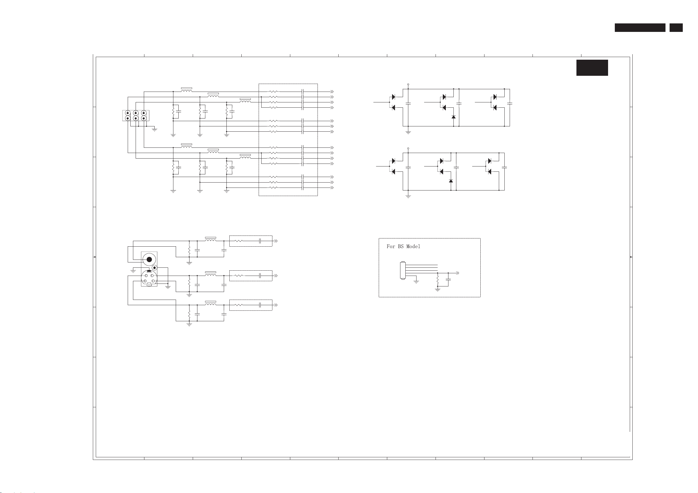
7 Circuit Diagrams and PWB Layouts Diagram
Scaler Board: Power (S-A01)22
Scaler Board: Lips & Inverter I/F (S-A02)23
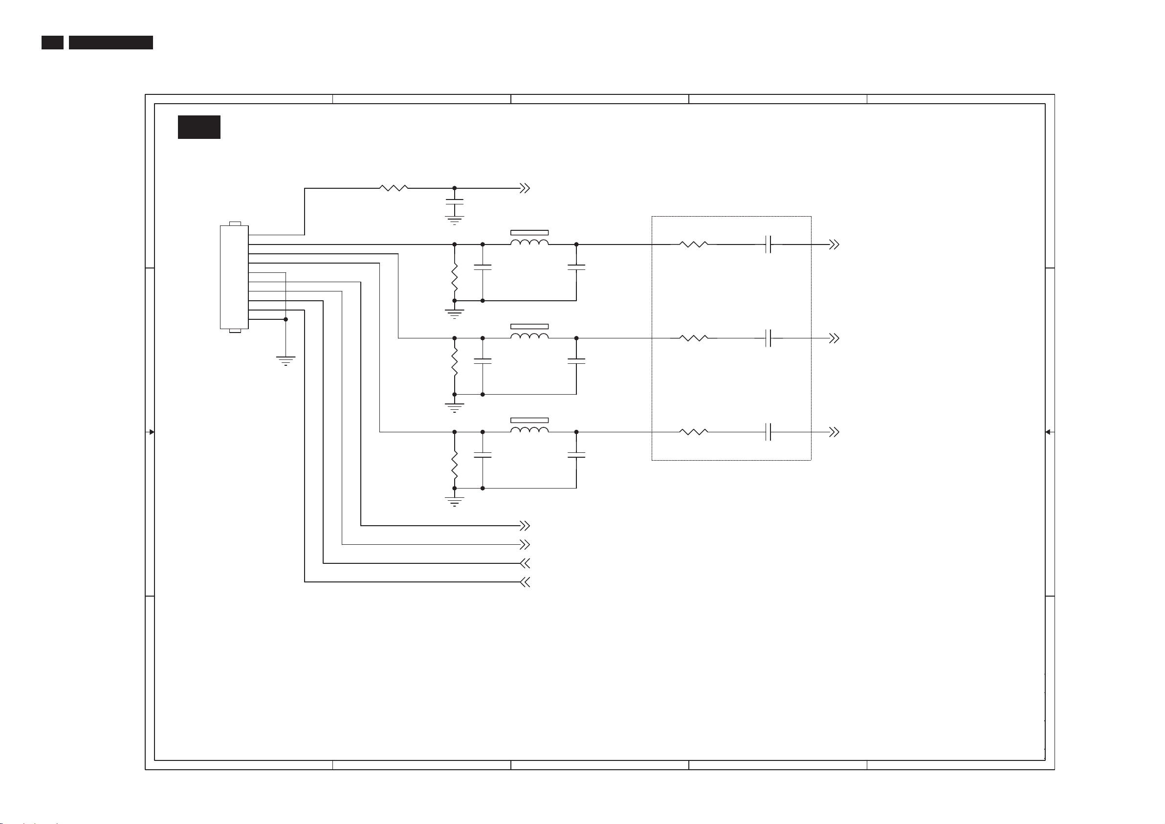
Scaler Board: Tuner (S-A03)24
Scaler Board: Video Input 1 (S-A04)25
Scaler Board: Side AV (S-A05)26
Scaler Board: DSUB Input (S-A06)27
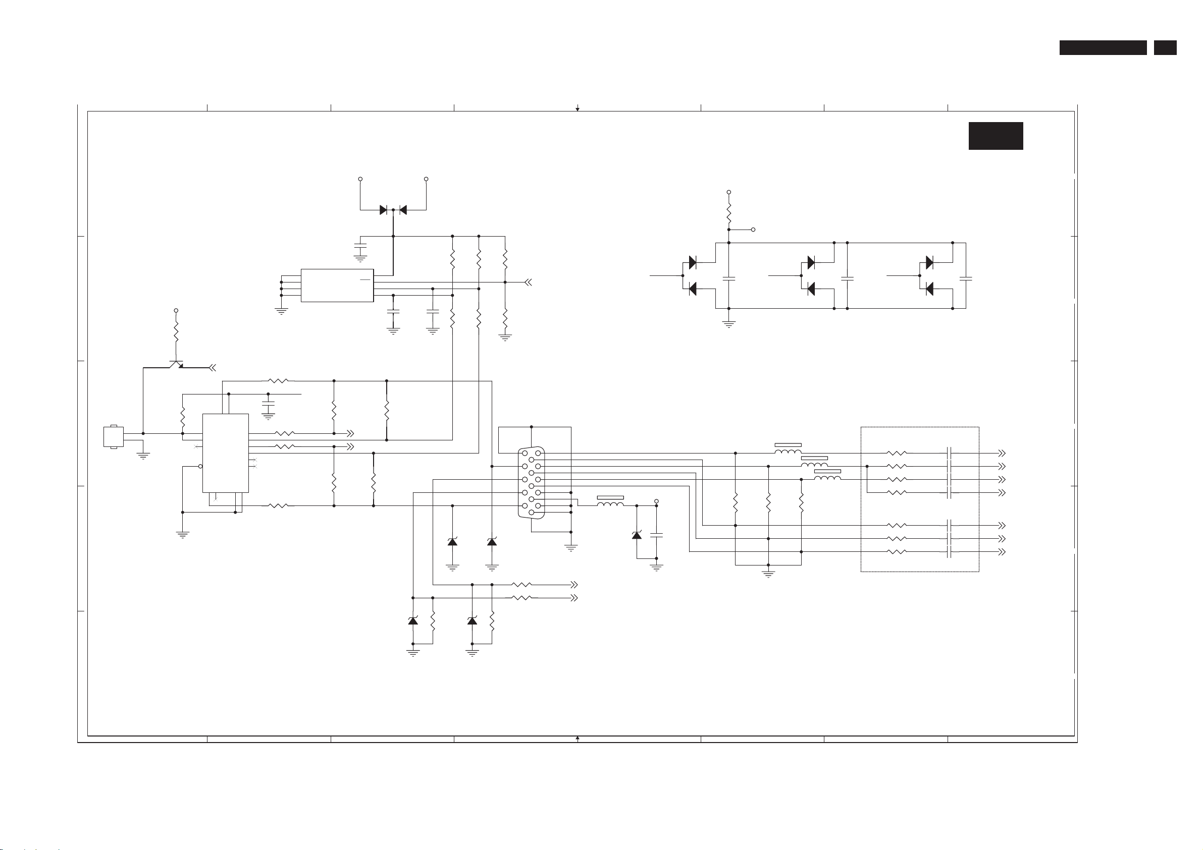
Scaler Board: DVI-D Input (S-A07) 28
Scaler Board: Scaler (S-A08)29
Scaler Board: Flash ROM & Memory (S-A09)30
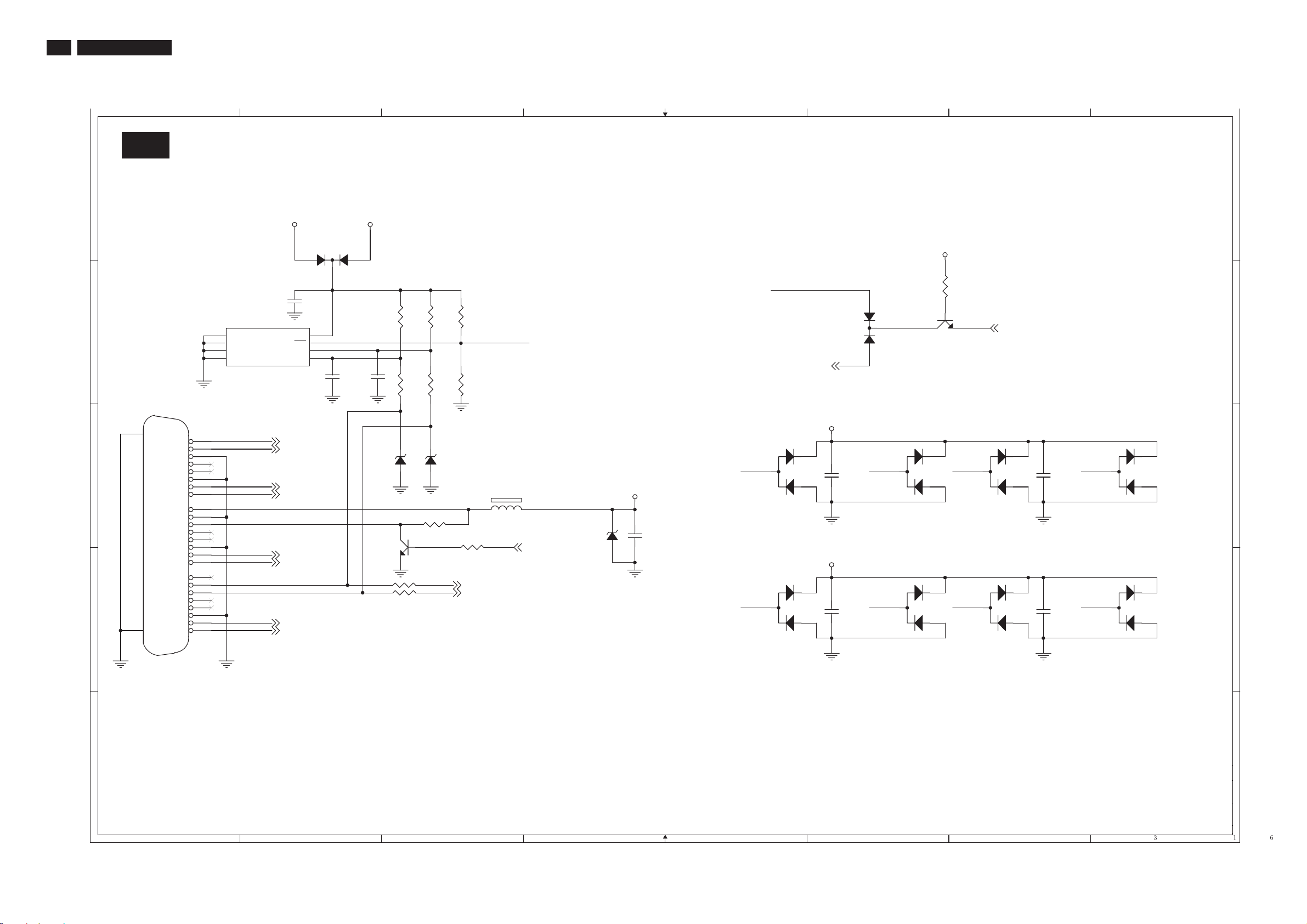
Scaler Board: Key, IR BD & ComPair I/F(S-A10)31
Scaler Board: ITV I/F (S-A11)32
Scaler Board: Panel I/F (S-A12) 33
Scaler Board: Audio I/F (S-A13) 34
Scaler Board: Audio MUX (S-A14)35
Scaler Board: Audio Amplifier (S-A15)36
Waveform Diagram 43-44
Keyboard Control Panel (K)45
IR & LED Panel (I)48
Side AV Panel (AV)51
Power Panel (P)54
8 Alignments 57
9 Circuit Descriptions, Abbreviation List, and IC Data
Sheets 64
Abbreviation List 67
IC Data Sheets 70
Exploded View 78
10 Recommended / Spare Parts List 74
Styling Sheet 74
Recommended Parts List 77
Spare Parts List 78
11 Different Parts List 90
12 Revision List 91
040407
©
Copyright 2007 Philips Consumer Electronics B.V. Eindhoven, The Netherlands.
All rights reserved. No part of this publication may be reproduced, stored in a
retrieval system or transmitted, in any form or by any means, electronic,
mechanical, photocopying, or otherwise without the prior permission of Philips.
Published by CS 0766 BG CD Customer Service Printed in the Netherlands Subject to modification EN 3122 785 17051
Page 2

2
TPS1.1A LA
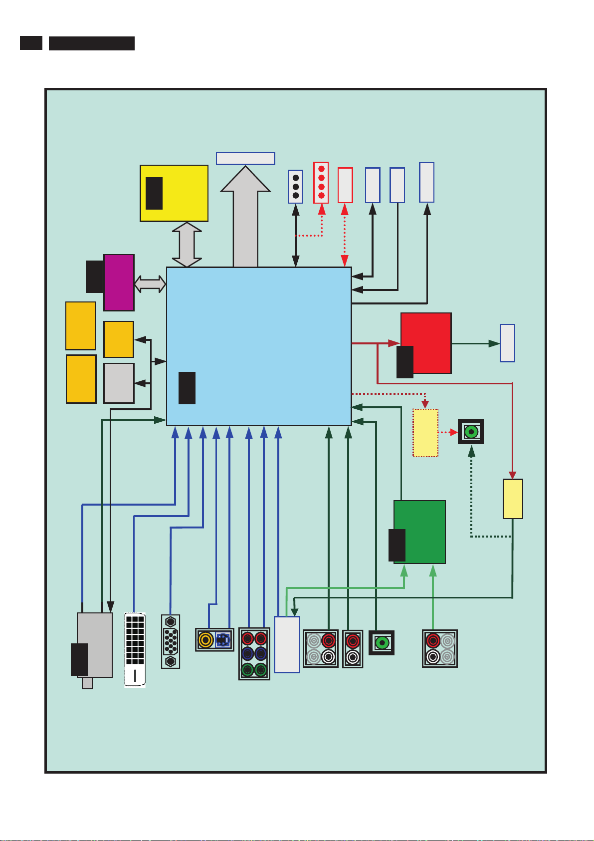
1. Technical Specifications,Connections,and Chassis Overview
1.Technical Specifications,Connections,and Chassis Overview
Index of this chapter:
1.1 Technical Specifications
1.2 Connections
1.3 Chassis Overview
Notes:
Figures below can deviate slightly from the actual situation,
due to the different set executions.
Specifications are indicative (subject to change)
1.1 Technical Specifications
Ambient conditions:
Ambient temperature: 15°C~35°C
Relative humidity : 25% ~ 75%.
1.2 Connections
1.2.1 Signal Connector
Connectors: From Right to Left
1.Tuner: PAL D/K for 93 model
1.1.1 Technical Specifications
Type : LCD
Outline dimensions : 626.0 mm(H) x 373.0 mm(V) x 44.1(D)
Pitch (mm) : 421.5.um(H) x 140.5um(V) (26")
Pixel format : 1366 horiz. by 768 vert. pixels
Color pixel arrangement : RGB vertical stripe
Display surface : Hard coating(3H),Anti-glare treatment
Number of color : 16,777,216 colors ( 8 bits)
Backlight : 17 EEFL(26")
Active area (WxH) : 575.769mm x 323.712mm (26")
View angle : Viewing angle free(R/L 178(Typ.),U/D
Contrast ratio : Typical 700 : 1(26")
Luminance of white : 500 cd/m²(Center 1 points, Typ.)
Supported video formats:
mm (Typ.)(26")
: 760.0 mm(H) x 450.0 mm(V) x 47.4(D)
mm (Typ.)(32")
: 510.75 .um(H) x 170.25um(V)(32")
of the front polarizer
: 16 CCFL(32")
: 697.68mm X 392.26 mm(32")
178(Typ.) (26")
: Viewing angle free(R/L 176(Typ.),U/D
176(Typ.))(32")
Typical 1500 : 1(32")
720 X 480i 60Hz
720 X 576i 50Hz
720 X 480P 60Hz
720 X 576P 50Hz
1280X 720P 50Hz
1280X 720P 60Hz
1920X1080i 50Hz
1920X1080i 60Hz
1920X1080p 50Hz
1920X1080p 60Hz
1.1.2 Sound
Sound system : 2CS, NICAM B/G (5.5-5.85), NICAM D/K (6.5-5.85),
Maximum power:2X5
NICAM I (6.0-6.52), stereo for all (should be in line
with RF system of each region)
2.Compair
3.AV1 audio IN : AV1 and S-Video shared audio R/L(RCA jack)
4.AV1 IN : Composite video input (AV1)
5.CVI IN : Component input with YPbPr format with audio R/L.
6.PC audio IN: audio R/L(mini-jack).
7.PC IN: VGA input (D-SUB connectors)
8.DVI-D : digital PC and video input
9.Earphone : earphone jack
10.AV2 IN : Composite video input (AV2 side)
11.AV2 audio IN : AV2 and S-Video side audio R/L(RCA jack)
12.S-Video IN : S-video input (S-Video side)
1.2.2 Input Signal
1.2.2.1 signal type
PC Signal
Analog Video :15 pin D-Sub
Digital Video :24-pin DVI-D connect connector, Single
Audio signal :Mini-jack audio input
TV Signal
RF signal : Aerial or cable via RF connector,
RF input level -10mV (80dBuV) typical, terminated with
1.1.3 Miscellaneous
Power supply
AC-input : 90V ~ 264VAC,50/60±2Hz
Power consumption :
Normal:
1.PC Mode TYP 100 W[Smart picture as "Normal" ] (with audio)(26")
PC Mode TYP 145 W[Smart picture as "Normal" ] (with audio)(32")
2.TV Mode TYP 100 W [Smart picture as "Rich"] (with audio)(26")
TV Mode TYP 145 W [Smart picture as "Rich"] (with audio)(32")
Maximum: 130W (with audio)(26")
170W (with audio)(32")
Power cord length : 1.8M
Power cord type : 3 lead with earth plug , plugable
(US type)
Power indicator : LED (On: blue ,Sleeping mode: Amber )
Auto power saving : EPA, Nutek, VESA DPMS
Horizontal scan : 30 ~ 61KHz
Vertical scan : 56 ~ 75 Hz
Component Y Pb Pr with RCA connector ( Video , Audio input ) Specification
Support:
Support: 480i/p, 720p/60Hz, 1080i/60Hz
PAL B/G
PAL D/K
I and SECAM B/G D/K for 98 model
I and NTSC-M for 79 model
Rx/Tx communicate
12
0.7 Vp-p linear, positive polarity and
separate Sync ( TTL level, positive or
negative polarity )
TMDS link according to DVI specification
input impedance of 75W.
Transient response: < 250 nS.
Sound (5.5MHz) suppression: > 55dB.
Chroma (4.43MHz) suppression: > 25dB.
Y/C separation: > 20dB.
China/93
AP/98
AP/79
PAL D/K
PAL B/G I SECAM B/G D/K
PAL B/G I NTSC-M
11
Video Y : 700mV, Pb, Pr, : ± 350mV,
Impedance : 75W
Audio : L/R input
Nominal : 0.5 V rms.
Maximum : 1.5 V rms. Impedance > 10 kW
Note : the input will be overloaded
10
when the signal > 1.5 V rms.
9
Page 3
1. Technical Specifications,Connections,and Chassis Overview
TPS1.1A LA
3
S-Video with S terminal (Video, Audio input) Specificati on
Support : PAL, NTSC and SECAM colour system
Composite with S terminal (Video, Audio input) Specification
Support : PAL, NTSC and SECAM colour system
DVI input with DVI connector, support HDCP Specification
upport : 480i/p, 720p/60Hz, 1080i/60Hz
S
Video - Y : 1Vpp , C : 300 mV pp
-Impedance : 75W.
Audio L/R input (share with Composite Audio input)
Nomi nal : 0.5 V rms.
Maximum : 1.5 V rms. Impedance > 10 kW.
Note : the input will be overloaded when the signal > 1.5 V rms.
Video - : 700mV Video, 300 mV -Sync
Impedance : 75W.
Audio L/R input (share with Composite Audio input)
- Nominal : 0.5 V rms.
Maximum : 1.5 V rms, Impedance > 10 kW.
Note : the input will be overloaded when the signal > 1.5 V rms.
Video - Digital interface with 4 channels TMDS signal
Impedance : 100W.
Audio L/R input
- Nominal : 0.5 V rms.
Maximum : 1.5 V rms.-Impedance > 10 K
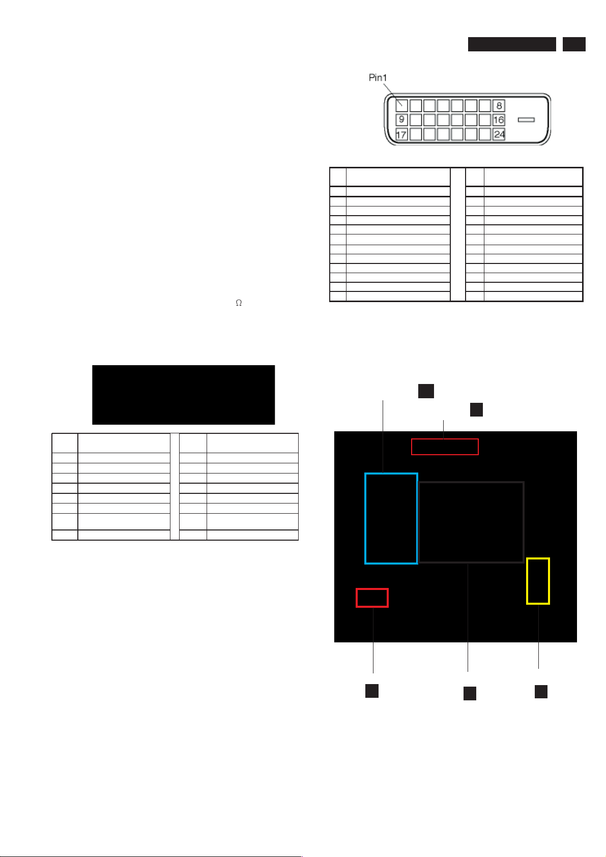
D-sub Pin assignment
DVI Pin assignment
PIN
No.
1 T.M.D.S. Data2- 13 No connect
2 T.M.D.S. Data2+ 14 +5V Power
3 T.M.D.S. Data2/4 Shield 15 Ground (for +5V)
4 No connect 16 Hot Plug Detect
5 No connect 17 T.M.D.S. Data06 DDC Clock 18 T.M.D.S. Data0+
7 DDC Data 19 T.M.D.S. Data0/5 Shield
8 No connect 20 No connect
9 T.M.D.S. Data1- 21 No connect
10 T.M.D.S. Data1+ 22 T.M.D.S. Clock Shield
11 T.M.D.S. Data1/3 Shield 23 T.M.D.S. Clock+
12 No connect 24 T.M.D.S. Clock-
SINGAL
PIN
No.
SINGAL
1.3 Chassis Overview
PIN
No.
1 Red video input 9 DDC +5V
2 Green video input /SOG 10 Logic ground
3 Blue video input 11 GND
4 GND 12 Serial data line (SDA)
5 GND– cable detect 13 H. Sync / H+V
6 Red video ground 14 V. Sync
7 Green video ground 15 Data clock line (SCL)
8 Blue video ground
SINGNAL
PIN
No.
SINGNAL
Power board
IR board
IR
P
Key board
K
Scaler board
S
SideAV board
AV
AV
Page 4
setoN dna ,sgninraW ,snoitcurtsnI ytefaS.2
2. Safety Instructions, Warnings and Notes
4 TPS1.1ALA
:retpahc siht fo xednI
sgninraW 2.2
setoN 3.2
snoitcurtsnI ytefaS 1.2
snoitcurtsnI ytefaS1.2
r snoitaluger ytefaS gniwollof eht eriuqe gnirud :riaper a
.)AV 008 >( remrofsnart
lacitnedi stnenopmoc yb ylno ynA .seno lanigiro eht ot
o( noitutitsbus tnenopmoc rehto yam )epyt lanigiro naht reht
ro erif fo ksir esaercni .drazah kcohs lacirtcele
taht eriuqer snoitaluger ytefaS retfa eb tsum tes eht ,riaper a
:stniop gniwollof eht
.spmalc elbac detnuom
.egamad lanretxe
.noitcnuf reporp
edis yradnoces eht dna gulp rewoP evah taht stes rof ylno(
,stcefed rof tenibac eht kcehC• yna fo gnihcuot tneverp ot
.remotsuc eht yb strap renni
.)3 lennahc( CSTN rof zHM 52.16
( htiw
( noitarepo
noitalosi na aiv rewoP CA/sniaM eht ot tes eht tcennoC•
lobmys eht yb detacidni ,stnenopmoc ytefas ecalpeR•
,
ot noitnetta ralucitrap ni yaP .noitidnoc lanigiro sti ni denruter
eht htiw meht xif dna yltcerroc seert eriw eht etuoR•
rof dael rewoP CA/sniaM eht fo noitalusni eht kcehC•
rof droc rewoP CA/sniaM eht fo feiler niarts eht kcehC•
CA/sniaM eht neewteb ecnatsiser CD lacirtcele eht kcehC•
:)ylppus rewop detalosi rewoP CA/sniaM a
eriw a tcennoc dna droc rewoP CA/sniaM eht gulpnU.1
.gulp rewoP CA/sniaM eht fo snip owt eht neewteb
noitisop "NO" eht ot hctiws rewoP CA/sniaM eht teS.2
.)!deggulpnu droc rewoP CA/sniaM eht peek(
eht fo snip eht neewteb eulav ecnatsiser eht erusaeM.3
eht fo gnidleihs latem eht dna gulp rewoP CA/sniaM
gnidaer ehT .tes eht no noitcennoc lairea eht ro renut
.mhoM 21 dna mhoM 5.4 neewteb eb dluohs
eht neewteb eriw eht evomer dna ,tes eht "FFO" hctiwS.4
.gulp rewoP CA/sniaM eht fo snip owt
setoN citamehcS2.3.2
.)mho
.tbuod
redloS eerf-daeL3.3.2
.sdrawno
( tuohtiw dna )
( yb-dnats ni dna ) era seulav esehT .)
detacidni srotcudnocimes ehT• ni dna margaid tiucric eht ni
cretni era ,stsil strap eht eht htiw noitisop rep elbaegnah
.srotcudnocimes eseht no noitacidni
dna ”cigoL orP“ ,”ybloD“ era ,”lobmys D-elbuod“ eht
.seirotarobaL ybloD fo skramedart
mho ni era seulav rotsiser llA• si reilpitlum eulav eht dna ,s
.)mhok 2.2 setacidni
tlum on htiw seulav rotsiseR• htiw detacidni eb yam reilpi
era seulav roticapac llA• ( sdaraf-orcim ni nevig =µ 01x
9-
01x =n( sdaraf-onan
e( noitacidni tniop lamiced .)Fp 2.2 setacidni 2p2 .g.
-dael gnicudorp si EC spilihP 5002.1.1 morf )FBP( stes eerf
01x =p( sdaraf-ocip ro ,)
.seulav tcerroc eht rof selbat ytisrevid eht ot
rab ruoloc a htiw )5 retpahc ees( edoM tluafeD ecivreS
detats sselnu zHk 1 :R ,zHk 3 :L( dnuos oerets dna langis
ro ,LAP rof zHM 52.574 ta reirrac erutcip dna )esiwrehto
segatlov dna smrofevaw eht erusaem ,yrassecen erehW•
eht erusaeM .langis lairea )
lamron ni htob noitces ylppus rewop eht ni segatlov
.slobmys etairporppa eht fo snaem yb detacidni
epyt eht fo evitcepserri ,tinu eht ni srotcudnocimes
.seirotarobaL ybloD morf esnecil rednu derutcafunaM•
2K2 .g.e( noitacol tniop lamiced eht etacidni ot desu netfo
022 setacidni R022 ro E022 .g.e( "R" na ro "E" na rehtie
6-
21-
,)
.)
eht sa reilpitlum eulav eht esu osla yam seulav roticapaC•
refeR .seirav egasu tnenopmoc setacidni )*( "ksiretsa" nA•
straP erapS eht ni detsil era seulav tnenopmoc tcerroc ehT•
yna si ereht nehw tsil siht kcehc syawla ,eroferehT .tsiL
sgninraW2.2
ocimes rehto ynam dna sCI llA• ot elbitpecsus era srotcudn
id citatsortcele DSE( segrahcs
rd efil ecuder nac riaper gnirud ,taht erus ekaM .yllacitsa
ra uoy ,riaper gnirud sa laitnetop emas eht htiw detcennoc e
:tnempiuqe noitcetorp DSE
ams( 3DSE tik etelpmoC– ,dnabtsirw ,tamelbat ll
lbac noisnetxe ,xob noitcennoc 2284 )elbac htrae dna e
.17601 013
.99931 443 2284 retset dnabtsirW–
.noitces
."NO" dehctiws si
lp esu ,tes eht ngila uoy nehW• .sloot latem naht rehtar citsa
trohs yna tneverp lliw sihT a fo regnad eht dna stiucric
.elbatsnu gnimoceb tiucric
gnildnah sseleraC .)
peeK .ecnatsiser htiw dnabtsirw a yb tes eht fo ssam eht
elbaliavA .laitnetop emas siht ta osla sloot dna stnenopmoc
egatlov hgih eht ni stnemerusaem gnirud luferac eB•
tinu eht elihw stnenopmoc rehto ro seludom ecalper reveN•
setoN3.2
lareneG1.3.2
eht ot drager htiw smrofevaw dna segatlov eht erusaeM•
( dnuorg )renut =( sissahc
idni era smargaid eht ni nwohs eht ni meht erusaeM .evitac
( dnuorg toh ro ,)
gnidneped ,)
smrofevaw dna segatlov ehT .yrtiucric fo aera detset eht no
:noitacifitnedI tigid-41 a sevig etalp epyt a fo enil mottob ehT
.)71 keew
: LEDOM
:ON.DORP
01/8699FP23
efer 6 dna 5 stigiD .rebmun laires stigid ,raey noitcudorp eht ot r
6002 si ti woleb elpmaxe ni( keew noitcudorp ot refer 8 dna 7
MUIGLEB NI EDAM
zH06/05V042-022
~
W821
100000 7160A1 GA
S
elpmaxe rebmun laireS 1-2 erugiF
rf-dael laiceps eht fo sseldrageR syawla ton si hcihw( ogol ee
es lla taert tsum eno ,)detacidni sdrawno etad siht morf st
.woleb debircsed sa selur eht ot gnidrocca
FHU+H+S+FHV
ALE0.3JB
spe.420_23560_E
606031
P
b
ogol eerf-daeL 2-2 erugiF
os ygolonhcet eerf-dael ot euD detcepser eb ot evah selur em
:riaper a gnirud pohskrow eht yb
Page 5

it gniredlos eerf-dael ylno esU• redro htiw 503CAS spilihP n
2. Safety Instructions, Warnings and Notes
TPS1.1A LA 5
,deriuqer si etsap redlos eerf-dael fI .60100 941 2260 edoc
utcafunam eht tcatnoc esaelp gniredlos ruoy fo rer
uaceb dediova eb dluohs spohskrow ot ysae ton si etsap es
.eldnah ot dna erots
t redlos etauqeda ylno esU• eerf-dael rof elbacilppa sloo
,C°004 evoba serutarepmet diovA fo tuo-raew esiwrehto
rd esaercni lliw spit .deyortsed eb lliw diulf-xulf dna yllacitsa
,spit fo tuo-raew diova oT ro tnempiuqe desunu ”ffo“ hctiws
.taeh ecuder
it gniredlos eerf-dael fo xiM• gniredlos dedael htiw strap/n
HP tub elbissop si strap/nit ylgnorts sdnemmocer SPILI ot
diova ylluferac ,dediova eb tonnac siht fI .semiger dexim
lo morf tnioj-redlos eht raelc .nit wen htiw redlos-er dna nit d
strap-eraps lanigiro ylno esU• .slaunaM-ecivreS eht ni detsil
.seinapmoc lanretxe ta desahcrup
,stnenopmoc dna nit gniredlos lliw strap eraps dedeen lla
t fo dne eht llit elbaliava eb riaper eht roF .doirep ecivres eh
.segnahc gnihton stes hcus fo
raob eht rehtehw tbuod fo esac nI htiw ro( ton ro eerf-dael si d
.)woleb snoitcurtsni osla ees( 503CAS
dlos naelc( ylhguoroht redlos-eD• fo xim diova ot stnioj re
.)syolla owt
noitacifitnedi MOB evitanretlA4.3.2
itcudorp ro( rebmun laires eht si )1-2 erugiF ees ,rebmun no
eht ,no etad siht morF .desopmoc tigid driht laires eht ni
GA :elpmaxe( rebmun 2 fo rebmun eht setacidni )1000005330B
nihtiw etsap redlos fo esu ,lareneg nI .tnempiuqe
:elba eb tsum loot redlos ehT .nit gniredlos
.C°004 tsael ta fo erutarepmet pit-redlos a hcaer oT–
.pit-redlos eht ta erutarepmet detsujda eht esilibats oT–
.snoitacilppa tnereffid rof spit-redlos egnahcxe oT–
dnuora fo erutarepmet a taht os loot redlos ruoy tsujdA•
.tnioj redlos eht ta desilibats dna dehcaer si C°083 - C°063
.ces 4 ~ deecxe ton dluohs tnioj-redlos eht fo emit gnitaeH
eb ot sah )seitidommoc( lairetam dradnats detsil toN
dedael gniniatnoc ,5002.1.1 erofeb decudorp stes roF•
:dohtem gniwollof eht esu nac uoy ,)seigolonhcet dexim
gnisu nehw ,redlos ot erutarepmet tsehgih eht esu syawlA•
• .kcohs lacirtcele ot erusopxe diova ot esnes sekam tI
• segatlov tcepser syawlA eb ton yam emos elihW .
yaw eht ni egnahc a decudortni EC spilihP ,3002 rebmetpeS nI
GA :elpmaxe( 1 .M.O.B eno ylno si ereht neht ,)100005330B
GA :elpmaxe( 2 tnereffid owt era ereht neht ,)1000005330B
)RLC(
.level tnenopmoc
fo lliB( MOB evitanretla eht eht gnicudorp rof desu slairetaM
si tI .)tes VT fo ledom cificeps ledom VT emas eht taht elbissop
fo sepyt tnereffid owt .g.e htiw decudorp si tekram eht no
.s.M.E.O tnereffid owt morf gnimoc ,syalpsid
fo tigid driht eht ta gnikool yB ecivres eht ,rebmun laires eht
.M.O.B fo epyt eno naht erom si ereht fi ees nac naicinhcet
nac eH .htiw gnikrow si eh tes VT eht fo noitcudorp eht ni desu
vreS ruoY tA eht tlusnoc neht epyt nac eh erehw ,etis beW eci
.g.e( tes VT eht fo rebmuN noisreV epyT laicremmoC eht ni
rcs a hcihw retfa ,)21/5159WP82 sevig taht raeppa lliw nee
.desu s.M.O.B evitanretla fo rebmun eht tuoba noitamrofni
laires eht fo tigid driht eht fI 1 rebmun eht sniatnoc rebmun
2 a si tigid driht eht fI .tekram eht no tes VT eht fo noisrev
eht gniredro rof tnatropmi si siht tuoba noitamrofnI .s.M.O.B
!strap eraps tcerroc
Z...A sretcarahc eht dna 9...1 srebmun eht ,tigid driht eht roF
nac s.M.O.B tnereffid 53 = 62 sulp 9 :latot ni os ,desu eb nac
.rebmun laires eht fo tigid driht eht yb detacidni eb
riapeR leveL tnenopmoC ro )RLB( riapeR leveL draoB5.3.2
tlusnoc ,evitcefed si draob a fI ediced ot erudecorp riaper ruoy
no deriaper eb dluohs ti fi ro degnahcxe eb ot sah draob eht fi
syas erudecorp riaper ruoy fI degnahcxe eb dluohs draob eht
ti ,esiwrehtO .draob evitcefed eht no redlos ton od ,yletelpmoc
!gnigrahc kcab rof reilppus .M.E.O eht ot denruter eb tonnac
snoituacerP ecivreS lacitcarP6.3.2
elbissop a evah ot detcepxe era secruos emos elihW
etiuq fo srehto ,tcapmi suoregnad fo era laitnetop hgih
.drager ssel ni dleh semitemos era dna tnerruc detimil
ht ,sevlesmeht ni suoregnad detcepxenu esuac nac ye
a otni gnihcaer erofeB .dediova tseb era taht snoitcaer
.noitalusni egatlov hgih eht tset ot tseb si ti ,tes VT derewop
.noituacerp ecivres doog a si dna ,od ot ysae si tI
Page 6
6
TPS1.1A LA
3. Directions for User
3. Directions for User
You can download this information from the following websites:
http://www.philips.com/support
http://www.p4c.philips.com
OSD Menu list
1st Layer 2nd Layer 3rd Layer 4th Layer
PC Mode
Picture
Sound
Color temp
Normal
Warm
Cool
Brightness
Contrast
Auto adjust Yes
Manual adjust
Phase
Clock
Horizontal
Vertical
Smart sound
Personal
Speech
Music
Movie
Multimedia
Install
Settings
AVL
Language
Factory reset
Treble
Bass
Balance
OnVirtual surround
Off
On
Off
Full screenFeatures Picture format
4:3
English
Thai
Arabic
No
Yes
Page 7
3. Directions for User
TV / AV/ S-VIDEO / HD MODE
1st Layer 2nd Layer 3rd Layer 4th Layer 5th Layer
Picture
Sound
Features
Smart picture
Contrast
Brightness
Color
Sharpness
Tint
Color temp
Picture format
Smart sound
Settings
AVL
Timer
NR
Auto lock
Source list
Personal
Rich
Nature
Soft
Multimedia
Normal
Warm
Cool
Super zoom
4:3
Movie expand 14:9
Movie expand 16:9
16:9 subtitle
Widescreen
Personal
Speech
Music
Movie
Multimedia
Treble
Bass
Balance
OnVirtual surround
Off
On
Off
Clock
Start time
Stop time
Sleep timer
On
Off
Lock program
Change code Enter New Code Confirm Code
Clear all Start ?
TV
CVI
AV1
AV2 (side)
PC
DVI
TPS 1.1A LA
7
Page 8
8
Install
TPS1.1A LA
Language
Auto store Start ?
Manual store
Channel setting
Factory reset
3. Directions for User
English
Thai
Arabic
Auto store
Please wait
Prog. found
Frequency
MHzManual store
Start ?
Prog. no
Finetune
Store
Channel edit
Channel swap
Channel sort Sort ?
No
Yes
Store ?
Stored
Channel
Skipped
From
To
Exchange
ChannelName edit
Name
Active
Skipped
Exchange ?
Exchanged
Sorting … …
Sort complete
Page 9
4. Mechanical Instructions
4. Mechanical Instructions
Index of this chapter:
4.1 Assy/Panel Removal
4.2 Set Re-assembly
4.1 Assy/Panel Removal
Notes: Please put your machine on soft material to avoid to scrape
panel when you disassemble it.
Front view
TPS1.1A LA
Step 4. Remove shielding.
Remove 10 screws as Fig.5 and remove 10 screws as Fig6.
9
Fig.4
Back view
Step 1. Remove the stand.
Remove the four screws as Fig.2.
Step 2. Remove the Back cover assy.
Remove the 10 screws on the bottom side as Fig.3.
Fig.1
Fig.2
Fig.5
Fig.6
Step 5. Remove Scaler board, Power board, SideAV board and
IR board.
Remove 17 screws as Fig.7.
Step 3. Remove the Vase plate and Bracket-base.
Remove the 14 screws on the bottom side as Fig.4.
Fig.3
Fig.7
Page 10
10
Step 6. Remove frame-PCB.
Step 7. Remove Metal frame.
TPS1.1A LA
Remove 7 screws as Fig.8.
Remove 16 screws as Fig.9.
4. Mechanical Instructions
Fig.8
4.2 Set Re-assembly
To re-assemble the whole set, execute all processes in reverse
order.
Notes:
a. While re-assembling, make sure that all cables are placed
and connected in their original position.
b. Pay special attention not to damage the EMC foams at the
Fig.9
Fig.9
SSB shielding. Check that EMC foams are put correctly on
their places.
Fig.12
Service Position
Step 8. Remove Metal frame.
Remove 4 screws as Fig.10.
In warranty, it is not allowed to disassembly the LCD panel, even the
backlight unit defect.
Out of warranty, the replacment of backlight unit is a correct way
when the defect is cused by backlight (CCFL,Lamp).
Fig.10
Fig.11
Page 11
5. Service Modes, Error Codes and Fault Finding
TPS1.1A LA
5. Service Modes, Error Codes and Fault Finding
index of this chapter:
5.1 CSM
5.2 Factory Mode
5.
3 Repair Flow Chart
5.1 CSM
It can display CSM windows message when press Menu+123654 on the button (RC) remote control in normal operation mode.
Then choose The following information is displayed on screen:
CSM Item Contents Remark
1: Set Type 32TA2800/93 Project name
2: Production code 01234567890123 14 digit pr oduction-code(serial number)
3: SW-naming mainprocessor MST96889LD-LF SW-naming of Mstar/Tr ident
4: Code 1 0 0 0 0 0 Error codes in NVM/EEPROM (5 last logged errors)
5: Code 2 0 0 0 0 0 Error codes in NVM/EEPROM (5 first logged errors)
6: Key (HDCP) Enabled HDMI information whether HDCP-key is valid
7: NVM-naming 24C32-Without-BDS Contents per display-type
The real picture as below:
11
About error code,Please refer to the table below.
Error code Event
0x01 DDR error
0x02 IIC bus error
0x03 Tuner er ror
0x04 Demod err or
Page 12

12
TPS1.1A LA
5. Service Modes, Error Codes and Fault Finding
5.2 Factory Mode
It can enter Factory Mode
1. Press" Menu in normal operation mode to enter OSD.
2. Press "062596+Menu on the button (RC) remote control in OSD.
3. The screen will appear F3 content in the bottom, choose it and press the right key.
OSD behavior:
Before press number key change OSD item
Now remove previous function, press number key then press OK will change value
Item Description Range method of operation
//Actio n Items
0ExitFactory press O K.
1 AutoColor
//Switch Items
2PowerOn On/Off
3 AGING MODE turn<On> and no signal input On/Off
//ADC G ain & Offset
4 ADC_GA IN_R 0~255 Press Left and Right to c hange value
5 ADC_GA IN_G 0~255
6 ADC_GA IN_B 0~255
7 ADC_OFFSET_R 0~127
8 ADC_OFFSET_G 0~127
9 ADC_OFFSET_B 0~127
"""
"
PC: any pattern has black and white
YPbPr:SMPTEbar(color bar), any timing.
(values different by VGA and YPbPr)
Au t o Colo r c hanges those items
press O K. when autocolor, the OSD disappear, when
finished. OSD appear.
//Color Temperature (values different by AV,VGA,DTV,YPbPr)
10 CLR_TEMP_R Back-End Scaler R G B Gain 0~255 Press Left and Right to change value
11 CLR_TEMP_G 0~255
12 CLR_TEMP_B 0~255
//Tuner & Panel Id
13 EEPROM ID value different by type
The below pictures is for your reference:
Step1: press MENU+062596 in user mode.
The factory content:
Step2: choose F3 98 V1.77.74.3,press the right key, then
enter the factory mode.
Page 13
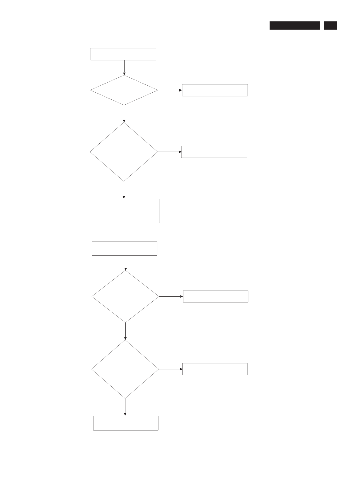
5.3 Repair Flow Chart
5. Service Modes, Error Codes and Fault Finding
1.No work/LED is off
TPS1.1A LA
13
Check if
power switch is
normal
Yes
Check
IR board CN0201
pin3=5V,pin5=5V
Yes
Check scaler board
U7105 pin1=24V,pin4=5V
2.No raster/picture too
dim
No
No
Replace Power switch
Check IR board
Check
power board
CN913,pin1=24V,
pin3=12V
Yes
Check
power board
IC920 pin2,IC970
pin2=12V
Yes
Check scaler board
No
No
Check Scaler board
Check IC920,IC970
Page 14
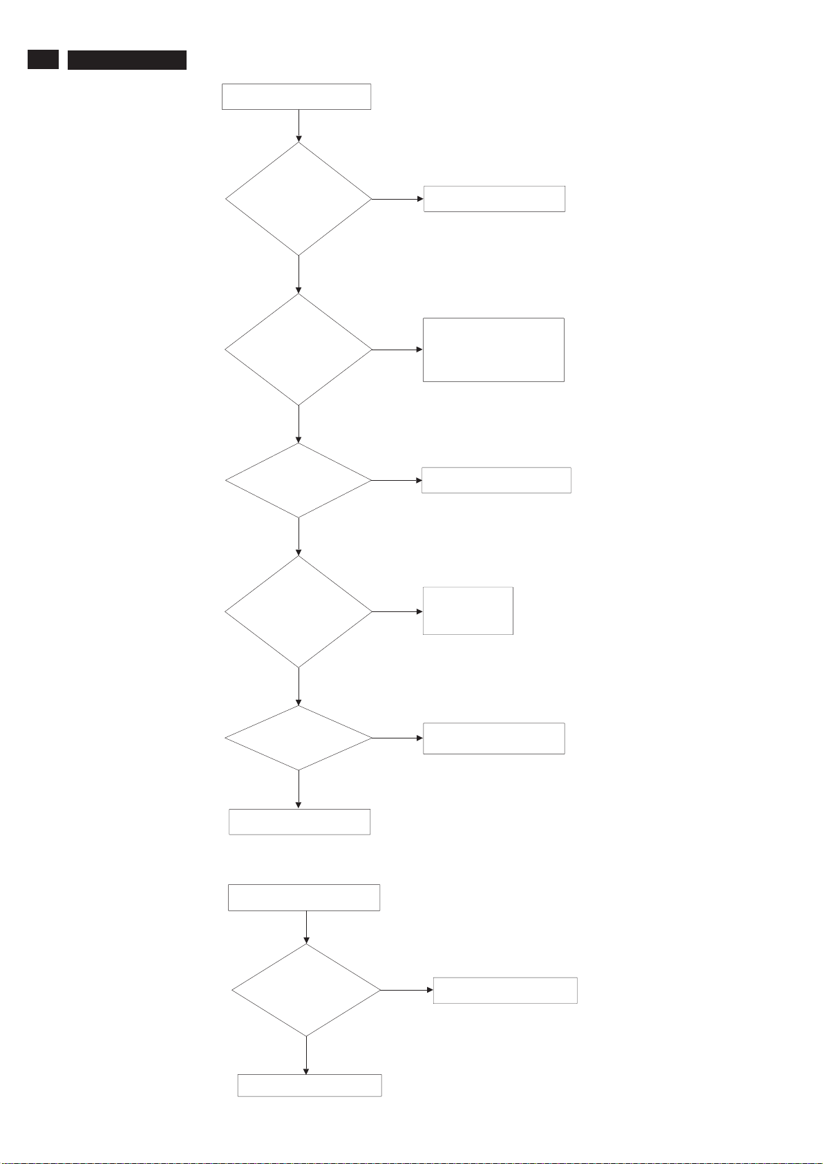
14
TPS1.1A LA
5. Service Modes, Error Codes and Fault Finding
3.No picture/LED is green
Check
scaler board U7105
pin1=24V,pin4=5V
Yes
No
Check power
Check if
working voltage
U7104 pin1=5V,
pin4=3.3V
Yes
Check if clock
source X4101
Yes
Check if
RGB,clk,H/V and
DE signal output 128
bits TTL
Yes
Check
resistors-network
No
No
No
No
Check circuit around
each regulator and
eliminate short and
open situation
Replace X4101
Try to replace
flash Rom
EEPROM
Replace bad resistorsnetwork
Yes
Replace LVDS cable
4.No TV sound
Check if
tuner TU2101 pin11
output IF signal
Yes
Check U4101
No
Replace TU2101
Page 15
5. Service Modes, Error Codes and Fault Finding
5.No earthphone sound
TPS1.1A LA
15
Check
U6301 pin33=3.3V
Yes
Check U6303
pin6= 5V
pin5,7=HPL/HPR
Yes
Replace Side AV Board
6.No remote function
No
No
Eliminate short and open
situation
Replace U6303
Tty another
remote control
Yes
Check IR receiver
7.LED and function
key poor
Check circuit around
control board and cable
between control board
and scaler board
No
Replace one good
remote control
Page 16
16
TPS1.1A LA
6. Block Diagram
Index of this chapter:
6.1
Wiring Diagram
6.2 Block Diagram
6.1 Wiring Diagram
6. Block Diagram
26TA2800 & 32TA2800 Wiring Diagram
095T8018 30948 FP
095T8014 3924 FP
095T8014 12936 FP
14 pin
11 pin
11 pin
30 pin
095T8014 7932 FP
3 pin
K
7pin 2pin
3pin
AV
2pin
10 pin
10 pin
7pin
IR
P
095T8014 11930 FP
095T8013 2967 FP
S
095T8013 2966 FP
095T8014 10932 FP
Page 17
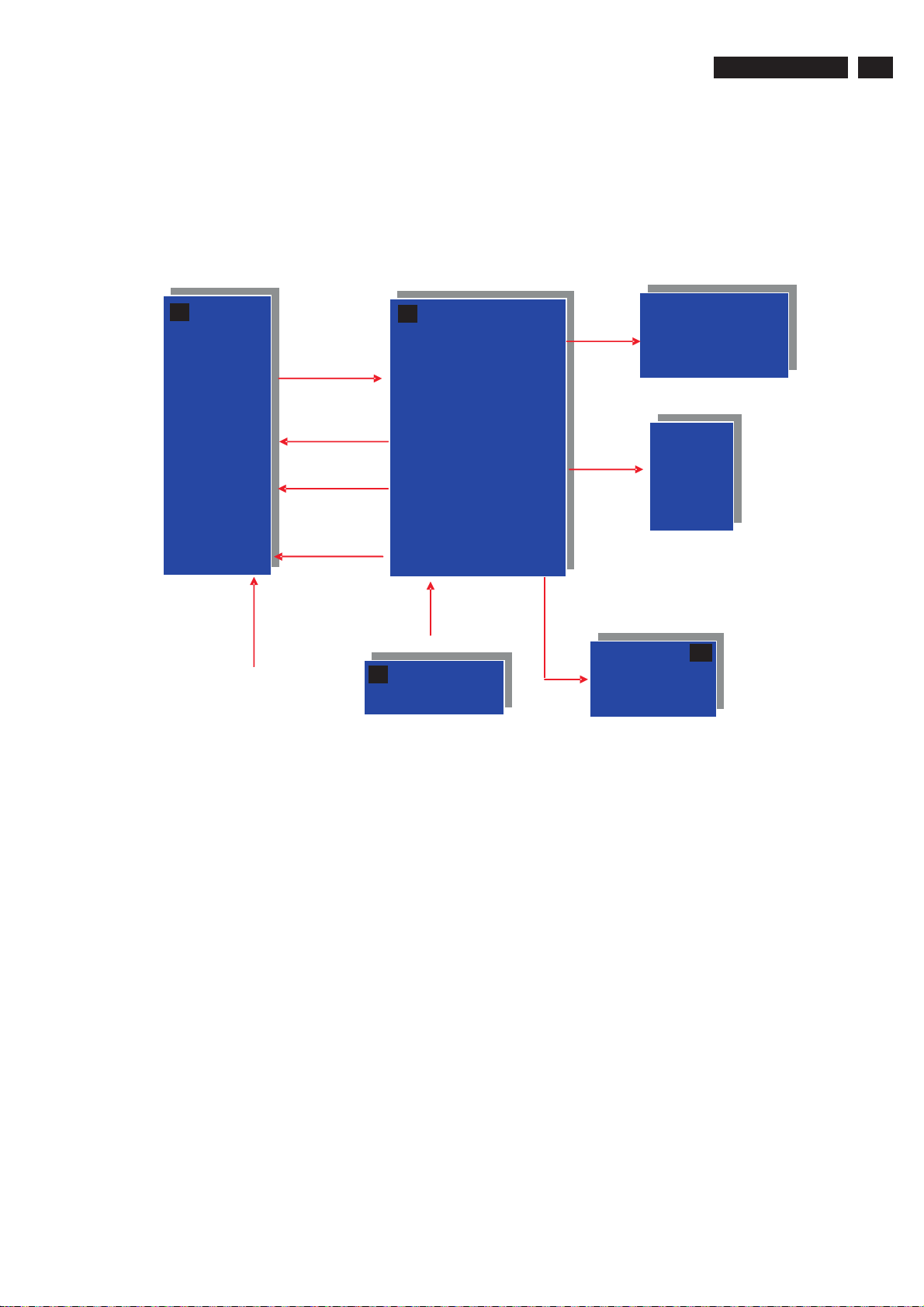
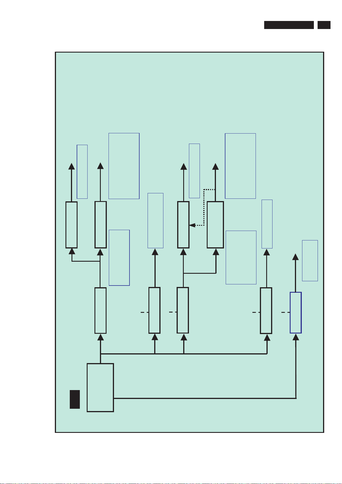
6.2 Block Diagram
6. Block Diagram
26 Wide, 32 Wide architecture Block Diagram""
TPS1.1A LA
17
P
Power
board
AC
Mains
Vcc
Bright_ADJ
Inverter_
ON/OFF
Stand-By
S
SCALER BOARD
MST96889L
74HC4052D MUX
TPA102
TPA3005D2
K
Control
Board
Side AV
Side AV
Board
( option )
LVDS Pa ne l
Speaker
2x5W
AV
Page 18
18
TPS1.1A LA
S-A09
SPI
SPI
DDR
DDR
6. Block Diagram
LCD Panel
LCD Panel
LVDS
LVDS
Com Pair
Com Pair
UART1
UART1
Cloning
Cloning
control
(ITV-1)
(ITV-1)
(ITV-2)
(ITV-2)
Video I/F
Video I/F
(5P)
(5P)
IR Board
IR Board
(7P)
(7P)
Key Board
Key Board
(3P)
(3P)
control
LIPS/PS
LIPS/PS
11P
11P
Function Block of main Board
24C02
24C02
DVI EDID
DVI EDID
24C02
24C02
DSUB EDID
DSUB EDID
CVBS0
CVBS0
S-A09
SIF0
SIF0
ROM
ROM
SPI Flash
SPI Flash
HDCP
HDCP
24C16
24C16
24C32
24C32
NVRAM
NVRAM
I2C
I2C
S-A08
MST96889L
MST96889L
AUL0, AUR0
AUL0, AUR0
AUL1, AUR1
AUL1, AUR1
Line-out
Line-out
DAC
DAC
AUL2, AUR2
AUL2, AUR2
TPA3005D2
TPA3005D2
S-A15
TPA6203A
TPA6203A
AUL3, AUR3
AUL3, AUR3
S-A14
74HC4052D
74HC4052D
AMP
AMP
1W AMP
1W AMP
MUX
MUX
2x(2P)
2x(2P)
(ITV-2)
(ITV-2)
HP/Bathroom
HP/Bathroom
Speaker
Speaker
TPA102
TPA102
L-R Speaker
L-R Speaker
S-A03
MM Tuner
MM TunerMM Tuner
R1,G1,B1
DVI-D
DVI-D
R1,G1,B1
D-SUB
D-SUB
DVI (CK,RX0,RX1,RX2)
DVI (CK,RX0,RX1,RX2)
Y0,C0
Y0,C0
CVBS1
CVBS1
S-Video
S-Video
CVBS
CVBS
CVBS2,Y1,C1
CVBS2,Y1,C1
Y,Pb,Pr (R2,G2,B2)
Y,Pb,Pr (R2,G2,B2)
Y,Pb,Pr (R0,G0,B0)
Y,Pb,Pr (R0,G0,B0)
Component-2
Component-2
Component-1
Component-1
(10P)
(10P)
SIDE AV
SIDE AV
CVBS
CVBS
Audio
Audio
Audio-1
Audio-1
Component
Component
PC Audio
PC Audio
Audio-2
Audio-2
Component
Component
Remark : Reserve only for ITV function
Remark : Reserve only for ITV function
Page 19
Speaker
Speaker
6. Block Diagram
TPS1.1A LA
SIDE AV
SIDE AV
TUNER
TUNERTUNER
ComPair
ComPairComPair
iTV
iTV
iTV
Level 1
Level 1
Level 1
19
AV 1
AV 1
IR BD
IR BD
Key BD
Key BD
I-BD
I-BD
26TA2800 BLOCK DIAGRAM
PWR I-BD
PWR I-BD
DSUB
DSUBDSUB
YPbPr
YPbPr
PC_Audio
PC_Audio
26”/32”LVDS
26 /3
2
LVDS
""
DVI-D
DVI-DDVI-D
PWR
PWR
Page 20
20
TPS1.1A LA
Speaker
Speaker
6. Block Diagram
SIDE AV
SIDE AV
ComPair
ComPairComPair
iTV
iTV
iTV
Level 1
Level 1
Level 1
32TA2800 BLOCK DIAGRAM
IR BD
IR BD
Key BD
Key BD
I-BD
I-BD
PWR I-BD
PWR I-BD
YPbPr2
YPbPr2
DSUB
DSUBDSUB
YPbPr1 AV 1
YPbPr1 AV 1
PC_Audio
PC_Audio
26”/32”LVDS
26 /32 LVDS
"
"
DVI-D
DVI-DDVI-D
PWR
PWR
Page 21
+1V8
+1V8
- U4101 (MST) : VDDC
- U4101 (MST) : VDDC
+3V3_STBY
+3V3_STBY
- U4101 (MST) :AVVD_DVI,
- U4101 (MST) :AVVD_DVI,
AVDDA,AVDD_MPLL,VDDP
AVDDA,AVDD_MPLL,VDDP
- U4202 (Flash ROM)
- U4202 (Flash ROM)
- U4102,3 (NVRAM)
- U4102,3 (NVRAM)
- U4104,5 (HDCP)
- U4104,5 (HDCP)
6. Block Diagram
+2V5
+2V5
- U4101 (MST) : VDDM
- U4101 (MST) : VDDM
+3V3
+3V3
- U4101 (MST) :AVDD_SIF,
- U4101 (MST) :AVDD_SIF,
AVDD_AV,AVDD_MemPLL,
AVDD_AV,AVDD_MemPLL,
VDDM
VDDM
- U4201, 3 (DDR, SDRAM)
- U4201, 3 (DDR, SDRAM)
- PANEL(+3.3V)
- PANEL(+3.3V)
TPS1.1A LA
21
U7106 (AME8815)
U7106 (AME8815)
Power management
S-A01
U7103 (AME8815)
U7103 (AME8815)
+5V_STBY
+5V_STBY
U7101 (AIC1596)
U7101 (AIC1596)
+24V
+24V
LIPS
LIPSLIPS
- For IR Board
- For IR Board
- U1101(24C02 :DSUB)
- U1101(24C02 :DSUB)
- U5101 (24C02 :DVI-D)
- U5101 (24C02 :DVI-D)
- For ITV use
- For ITV use
+5V_ITV
+5V_ITV
ITV_5V_SW
ITV_5V_SW
U7105 (AIC1596)
U7105 (AIC1596)
+24V
+24V
- U7401 (SyncSlicer)
- U7401 (Sync Slicer)
+5V
+5V
PWR_SW
PWR_SW
+24V
+24V
U7107 (AME8815)
U7107 (AME8815)
U7102 (AIC1596)
U7102 (AIC1596)
or (AIC1084/5)
or (AIC1084/5)
U7104 (AME8815)
U7104 (AME8815)
+5V
+5V
- TU2101 (TUNER)
- TU2101 (TUNER)
- U6201 (Audio MUX)
- U6201 (Audio MUX)
- U6302 (Bath AMP)
- U6302 (Bath AMP)
- U6303 (HP AMP)
- U6303 (HP AMP)
- PANEL(+5V)
- PANEL(+5V)
+12V_AUDIO
+12V_AUDIO
AU_PWR_SW
AU_PWR_SW
+24V
+24V
- U6301 (AUD AMP)
- U6301 (AUD AMP)
ITV_12_SW
ITV_12_SW
U7108 (AIC1596)
U7108 (AIC1596)
+12V_ITV
+12V_ITV
Q7110 (SI5441)
Q7110 (SI5441)
+12V
+12V
- For ITV use
- For ITV use
- PANEL(+12V)
- PANEL(+12V)
Page 22
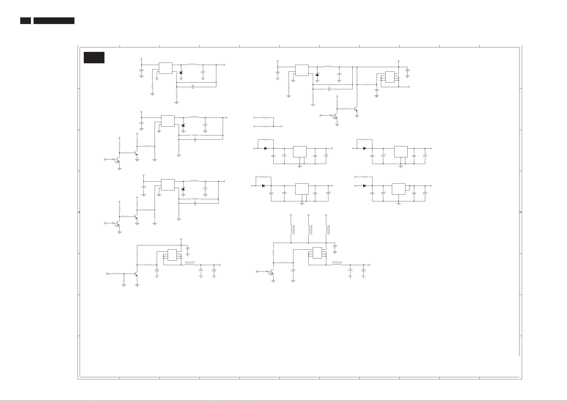
22
TPS1.1A LA
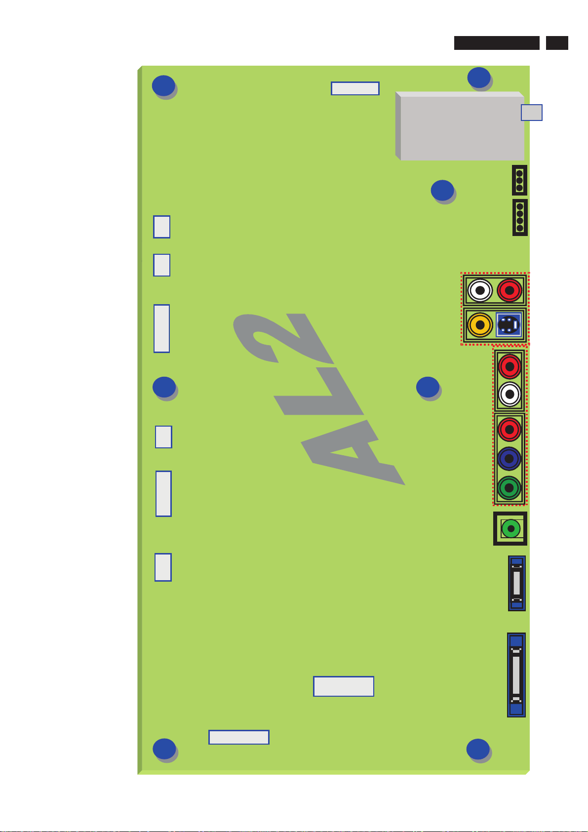
Scaler Schematic Diagram - PowerBoard
7. Circuit Diagrams and PWB Layouts
1
S-A01
A A
B B
+5V_STBY
R7117
47K(NC)
C C
ITV_5V_SW8
D D
AU_PWR_SW8
E E
2
2
3
1
+5V_STBY
3
1
R7120
1K(NC)
Q7101
MUN2211J(NC)
R7125
47K
R7128
1K
Q7107
MUN2211J
2
+24V
C7102
0.1uF
+24V
C7126
0.1uF(NC)
+24V
R7116
220K(NC)
R7118
3
100R(NC)
Q7104
2
BC847C(NC)
1
+24V
C7101
0.1uF
+24V
R7123
220K
R7126
3
100R
Q7106
2
BC847C
1
U7102
1
IN
5
ON/OFF
3 4
GND FB
AIC1596-33PM5
R7108
0R
U7108
1
IN
5
ON/OFF
3 4
GND FB
AIC1596-50P(NC)
R7129
0R(NC)
U7101
1
IN
5
ON/OFF
3 4
GND FB
AIC 1596-12PM5
R7101
0R(NC)
OUT
OUT
OUT
2
2
2
3
2
ZD7102
SSA34-E3
1
R7103 0R
C7105 0.1uF(NC)
R7109
0R(NC)
2
ZD7104
SSA34-E3(NC)
1
R7122 0R(NC)
C7129 0.1uF(NC)
R7127
0R(NC)
2
ZD7101
SSA34-E3
1
R7106 0R
C7106 0.1uF(NC)
R7110
0R(NC)
+12V
L7102
35uH
L7104
35uH(NC)
L7101
35uH
C7103
470uF 25V
C7127
470uF 25V(NC)
C7104
470uF 25V
4
+3V3_STBY
+5V_ITV
+12V_AUDIO
5
+24V
C7115
0.1uF
R7136
+5V
0R05
R7135
0R05(NC)
R7114
0R05(NC)
D7104
+3V3_STBY
+5V_PANEL +3V3_PANEL
1 2
AK
S1D
R7111
0R05(NC)
D7101
1 2
AK
GF1D(NC)
C7118
0.1uF
C7107
0.1uF(NC)
+5V_PANEL+5V_ITV
10uF 50V(NC)
1
IN
5
ON/OFF
3 4
GND FB
AIC1596-50PM5
R7121
0R
U7106
AME8815AEGT180Z
1
VIN
C7121
10uF 50V
U7103
AME8815AEGT330Z(NC)
1
VIN
C7110
+12V
1
FB7101
220R
2
6
U7105
2
OUT
2
ZD7103
SSA34-E3
1
R7119
0R(NC)
PWR_SW8
VOUT
GND
TH
C7119
234
VOUT
GND
234
+5V_PANEL +3V3_PANEL
0.1uF
TH
C7108
0.1uF(NC)
1
FB7102
220R(NC)
2
L7103
35uH
R7113 0R
C7117 0.1uF(NC)
+5V_STBY
R7104
47K
3
2
1
+1V8
C7122
100uF 10V
100uF 10V(NC)
C7111
1
FB7103
220R(NC)
2
7
Q7103
MUN2211J
8
+5V_STBY
Q7111
C7109
0.1uF
C71200.1uF
4 5
3
2
1
C7137
220N
GS
D
D
D
D
D
D
SI5441DC
U7104
AME8815AEGT330Z
1
C7112
10uF 50V
U7107
AME8815BEGT250Z
3 2
VI VO
C7123
10uF 50V
C7116
470uF 25V
R7107
1K
R7102
22K
R7105
47K
3
Q7102
2
BC847C
1
R7112
0R05(NC)
D7102
1 2
+5V
AK
S1D
R7115
+3V3
0R05(NC)
D7105
1 2
+5V +2V5
AK
S1D
C7138
0.1uF
6
7
8
+5V
VIN
VOUT
GND
TH
234
4
TH
GND
1
C7114
0.1uF
C7124
0.1uF
9
+3V3
C7113
100uF 10V
C7125
100uF 10V
10
C7101 D2 C7102 A2
C7103 A3 C7104 D4
C7105 A3 C7106 D3
C7107 D5 C7108 D6
C7109 C8 C7110 D6
C7111 D7 C7112 C8
C7113 C9 C7114 C9
C7115 A5 C7116 A7
C7117 A7 C7118 C5
C7119 C6 C7120 D8
C7121 C6 C7122 C7
C7123 D8 C7124 D9
C7125 D9 C7126 B2
C7127 B4 C7128 E7
C7129 C3 C7130 F6
C7131 F7 C7132 F7
C7133 E3 C7134 F2
C7135 F3 C7136 F4
C7137 B8 C7138 A9
D7101 D5 D7102 C7
D7104 C5 D7105 D7
FB7101 E6 FB7102 E6
FB7103 E7 FB7104 F7
FB7105 F3 L7101 D3
L7102 A3 L7103 A7
L7104 B3 Q7101 C1
Q7102 B7 Q7103 B7
Q7104 C2 Q7105 E6
Q7106 E2 Q7107 E1
Q7108 F5 Q7109 F2
Q7110 E3 Q7111 A8
R7101 D2 R7102 A7
R7103 A3 R7104 B7
R7105 A8 R7106 D3
R7107 B7 R7108 A2
R7109 B3 R7110 D3
R7111 D5 R7112 C7
R7113 A7 R7114 C5
R7115 D7 R7116 C2
R7117 C1 R7118 C2
R7119 B6 R7120 C2
R7121 A6 R7122 C3
R7123 D2 R7124 E5
R7125 D1 R7126 D2
R7127 C3 R7128 E2
R7129 C2 R7130 F5
R7131 F1 R7132 F2
R7133 E2 R7134 F2
R7135 B5 R7136 B5
U7101 D3 U7102 A2
U7103 D6 U7104 C8
U7105 A6 U7106 C6
U7107 D8 U7108 B3
ZD7101 D3 ZD7102 A3
ZD7103 A6 ZD7104 B3
11
6
7
8
C7128
0.1uF(NC)
FB7104
1 2
220R
7
C7131
10uF 50V
C7132
0.1uF
PANEL_VCC
CP NR. CL6xxxx
Title
AL2 26TA2800 MAIN BOARD(DC-DC POWER)
Size Document Number Rev
E267G1ND8WPHNS (715T2441-1)
C
8
9
Date: Sheet of
10
116Friday, January 05, 2007
11
1
Q7105
4 5
GS
3
D
D
2
D
D
1
D
D
SI5441DC
6
6
7
8
1 2
3
C7133
0.1uF(NC)
FB7105
220R(NC)
C7135
10uF 50V(NC)
+12V_ITV
C7136
0.1uF(NC)
4
R7124
56K
R7130
3
75K
Q7108
PANEL_PWR8
2
MUN2211J
1
5
C7130
330N
Q7110
4 5
C7134
22nF(NC)
GS
3
D
D
2
D
D
1
D
D
SI5441DC(NC)
R7133
22K(NC)
R7134
4K7(NC)
R7132
47K
3
Q7109
2
BC847C(NC)
1
2
F F
G G
H H
ITV_12V_SW2,8
1
R7131
33K
Page 23
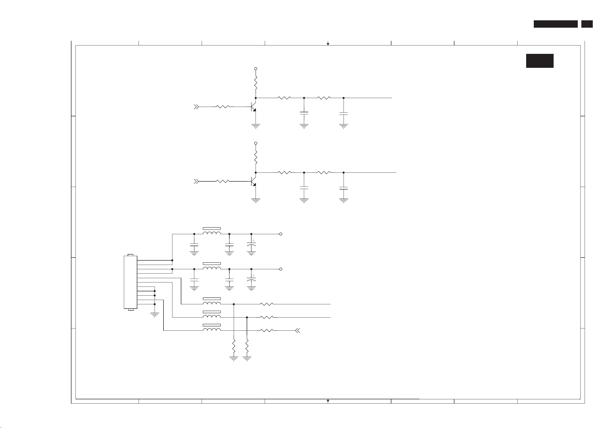
Scaler Schematic Diagram -Board Lips & Inverter I/FLips & Inverter I/F
1
2
7.Circuit Diagrams and PWB Layouts
3
4
5
6
7
TPS1.1A LA
8
23
+5V
A A
BL_ADJ8
B B
BL_EN8
C C
For LIPS/PS
CN7201
1
2
3
4
5
6
7
8
D D
9
10
11
R7201 10K
R7208 10K
FB7201
1 2
120R
C7205
0.1uF
FB7202
1 2
120R
C7208
0.1uF
1 2
FB7204 120R
2
2
C7206
0.1uF
C7209
0.1uF
R7202
4K7
R7203 0R05
3
Q7201
BC847C
1
+5V
R7205
1K
R7206 2K2
3
Q7202
BC847C
1
C7207
470uF 35V
C7210
100uF 25V
R7209 47R
+24V
+12V
R7204 10R
C7201
1U(NC)
R7207 10R
C7203
1U(NC)
BRIGHT_ADJ
BRIGHT_ADJ
C7202
0.1uF(NC)
INVERTER_ON_OFF
C7204
0.1uF
CN7201 C2
C7201 A4
C7202 A4
C7203 B4
C7204 B4
C7205 C2
C7206 C3
C7207 C3
C7208 C2
C7209 C3
C7210 C3
FB7201 C3
FB7202 C3
FB7204 D3
FB7205 D3
FB7206 D3
Q7201 A3
Q7202 B3
R7201 A3
R7202 A3
R7203 A3
R7204 A4
R7205 B3
R7206 B3
R7207 B4
R7208 B3
R7209 D3
R7210 D3
R7211 D3
R7212 D3
R7213 D3
S-A02
63391 11P 2.0MM
E E
1 2
FB7205 120R
1 2
FB7206 120R
R7212
0R(NC)
R7210 47R
R7211 47R
R7213
10K
INVERTER_ON_OFF
ITV_12V_SW 1,8
CP NR. CL6xxxx
Title
AL2 26TA2800 MAIN BOARD(LIPS & INVERTER I/F)
Size Document Number Rev
B
E267G1ND8WPHNS (715T2441-1)
1
2
3
4
5
Date: Sheet of
6
7
216Friday, January 05, 2007
8
1
Page 24
24
TPS1.1A LA
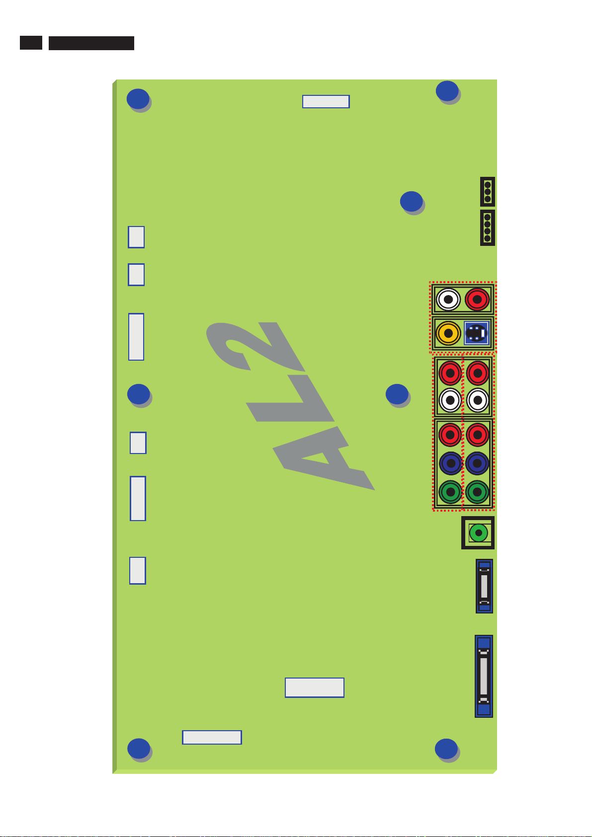
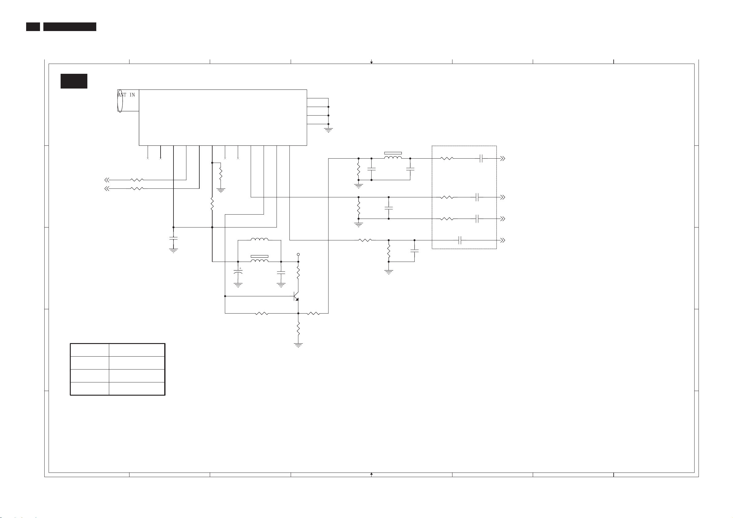
Scaler Schematic Diagram - TunerBoard
7. Circuit Diagrams and PWB Layouts
1
S-A03
A A
I2C_SCL8,11
B B
C C
I2C_SDA8,11
R2101 47R
R2105 47R
N.C.
TU2101
N.C
1
SCL
2
C2101
0.1uF
2
+5V
SDA
AS_TU
NC
AS_IF
3
4
5
6
R2107
0R(NC)
9
R2103
0R
3
2NDIFSOUND
10
11
22uH(NC)
1 2
C2 111
1000uF 16V
CVBS
L2101
FB2101
100R
R2113
4
15
TH1
16
TH2
17
TH3
18
TH4
AF O/P
+5V,IF
13
12
C2110
0.1uF
2
14
+5V
R2112
10K(NC)
3
Q2101
BC847C(NC)
1
R2114
TV_CVBS
R2104
75R 1%
TV_SIF
MONO
1 2
FB2102 30R
330P(NC)
C2103
R2108
2K2(NC)
R2110 10K(NC)
R2 111
10K(NC)
C2106
100P(NC)
22P
C2109
5
C2104
330P(NC)
R2102 47R
R2106 0R
R2109 0R
C2108 0.1uF(NC)
C2102 47N
C2105 0.1uF
C2107 0.1uF
6
TUNER_CVBS 8
SIFP0 8
SIFM0 8
AUMONO 8
7
C2101 C2
C2102 B6
C2103 B4
C2104 B5
C2105 B6
C2106 B5
C2107 B6
C2108 C6
C2109 C5
C2110 C3
C2111 C3
FB2101 C3
FB2102 B5
L2101 C3
Q2101 C3
R2101 B2
R2102 B5
R2103 B3
R2104 B4
R2105 B2
R2106 B5
R2107 B2
R2108 B4
R2109 B5
R2110 C4
R2111 C5
R2112 C4
R2113 C3
R2114 C4
R2115 D4
TU2101 A1
8
0R
R2115
0R(NC)
D D
TU2101MODEL
0R
CHINA (/93) FQ1256 MK5
AP (/98)
AP (/79)
E E
FQ1216ME MK5
FQ1216PN MK5
CP NR. CL6xxxx
Title
AL2 26TA2800 MAIN BOARD(TUNER)
Size Document Number Rev
B
E267G1ND8WPHNS (715T2441-1)
of
1
2
3
4
5
6
Date: Sheet
7
316January 05, 2007
8
1
Page 25
Scaler Schematic Diagram - Video Input 1Board
7.Circuit Diagrams and PWB Layouts
TPS1.1A LA
25
1
2
3
4
5
6
7
8
9
10
11
S-A04
2
1
2
1
+3V3_ESD
+3V3_ESD
C2204
0.1uF(NC)
C22210.1uF(NC)
D2202
3
BAV99(NC)
D2205
3
BAV99(NC)
D2204
BAS32L(NC)
D2208
BAS32L(NC)
CN2201 B1 CN2202 D1
2
C2205
0.1uF(NC)
1
2
AK
1
2
C2222
0.1uF(NC)
1
2
AK
1
BAV99(NC)
D2206
3
BAV99(NC)
2
3
C2206
0.1uF(NC)
1
2
C2223
0.1uF(NC)
1
CN2203 E7 C2201 B2
C2202 A5 C2203 A5
C2204 A7 C2205 A8
C2206 A9 C2207 A5
C2208 A5 C2209 B3
C2210 B3 C2211 B5
C2212 B5 C2213 B5
C2214 B5 C2215 B5
C2216 B5 C2217 C5
C2218 C2 C2219 C3
C2220 C3 C2221 C7
C2222 C8 C2223 C9
C2224 C5 C2225 C5
C2226 C5 C2227 D4
C2228 D3 C2229 D3
C2230 E4 C2231 E8
C2232 E3 C2233 E3
C2234 E4 C2235 F3
C2236 F3 D2201 A6
D2202 A7 D2203 A9
D2204 B8 D2205 C7
D2206 C8 D2207 C6
D2208 C8 FB2201 A2
FB2202 A3 FB2203 A3
FB2204 B2 FB2205 B3
FB2206 B3 FB2207 D3
FB2208 E3 FB2209 E3
R2201 B2 R2202 A4
R2203 A4 R2204 A4
R2205 A4 R2206 B3
R2207 B3 R2208 B4
R2209 B4 R2210 B4
R2211 B4 R2212 B4
R2213 B4 R2214 C4
R2215 C2 R2216 C3
R2217 C3 R2218 C4
R2219 C4 R2220 C4
R2221 D3 R2222 D2
R2223 E3 R2224 E2
R2225 E7 R2226 E3
A A
R_PR2
G_Y2
B_PB2
32659
1
4
8
7
PR1
Y1
PB1
CN2201
RCA JACK 2*3
B B
C C
R2215
75R 1%
R2201
1 2
FB2201 30R(NC)
C2201
10P(NC)
75R 1%(NC)
1 2
FB2204 30R
C2218
10P(NC)
R2216
75R 1%
R2206
1 2
FB2202 30R(NC)
C2209
10P(NC)
75R 1%(NC)
1 2
FB2205 30R
C2219
10P(NC)
R2217
75R 1%
R2207
75R 1%(NC)
1 2
FB2203 30R(NC)
C2210
10P(NC)
1 2
FB2206 30R
C2220
10P(NC)
R2202 47R(NC)
R2203 47R(NC)
R2204 47R(NC)
R2205 470R(NC)
R2208 47R(NC)
R2209 47R(NC)
R2210 47R(NC)
R2211 47R
R2212 47R
R2213 47R
R2214 470R
R2218 47R
R2219 47R
R2220 47R
C2202 47N(NC)
C2203 47N(NC) D2203
C2207 47N(NC)
C2208 1N(NC)
C2211 47N(NC)
C2212 47N(NC)
C2213 47N(NC)
C2214 47N
C2215 47N
C2216 47N
C2217 1N
C2224 47N
C2225 47N
C2226 47N
PR2+
Y2+
PB2+
SOY2
PR2-
Y2-
PB2-
PR1+
Y1+
PB1+
SOY1
PR1-
Y1-
PB1-
PR2+ 8
Y2+ 8
PB2+ 8
SOY2 8
PR2- 8
Y2- 8
PB2- 8
PR1+ 8
Y1+ 8
PB1+ 8
SOY1 8
PR1- 8
Y1- 8
PB1- 8
D2201
R_PR2 G_Y2 B_PB2
3
BAV99(NC)
D2207
PR1 Y1 PB1
3
BAV99(NC)
D D
1 2
R2222
CN2202JACK
7
9
8
1 2
E E
F F
G G
3 4
6
5
75R 1%
R2224
75R 1%
R2227
75R 1%
FB2207 30R
C2228
330P(NC)
1 2
FB2208 30R
C2232
330P(NC)
1 2
FB2209 30R
C2235
330P(NC)
R2221 47R
C2229
330P(NC)
R2223 47R
C2233
330P(NC)
R2226 47R
C2236
330P(NC)
C2227 47N
C2230 47N
C2234 47N
AV_CVBS 8
SV_Y0 8
SV_C0 8
CN2203
63385 5P 2.0mm (NC)
75R 1%(NC)
R_PR2
G_Y2
B_PB2
R2225
C2231
0.1uF(NC)
FBL2 8
1
2
3
4
5
H H
1
2
3
4
5
6
7
8
9
CP NR. CL6xxxx
Title
AL2 26TA2800 MAIN BOARD(VIDEO INPUT-1)
Size Document Number Rev
C
E267G1ND8WPHNS (715T2441-1)
Date: Sheet
10
of
416January 05, 2007
11
1
Page 26
26
TPS1.1A LA
Scaler Schematic Diagram - Side AVBoard
7. Circuit Diagrams and PWB Layouts
1
2
3
4
5
S-A05
A A
CN2301
10
9
8
7
6
5
4
3
2
1
B B
63370 10P 2.0MM
R2302 100R
75R 1%
75R 1%
75R 1%
R2304
R2306
R2301
C2302
100P(NC)
1 2
C2304
330P(NC)
1 2
C2307
330P(NC)
1 2
C2301
330P(NC)
HP_DET 8
FB2302 30R
FB2303 30R
FB2301 30R
C2305
330P(NC)
C2308
330P(NC)
C2310
330P(NC)
R2303 47R
R2305 47R
R2307 47R
C2303 47N
C2306 47N
C2309 47N
SIDE_CVBS 8
SIDE_SV_C1 8
SIDE_SV_Y1 8
CN2301 A1
C2301 C2
C2302 A2
C2303 A4
C2304 A2
C2305 A3
C2306 B4
C2307 B2
C2308 B3
C2309 B4
C2310 C3
FB2301 B2
FB2302 A2
FB2303 B2
R2301 C2
R2302 A2
R2303 A3
R2304 A2
R2305 B3
R2306 B2
R2307 B3
C C
D D
SIDE_AU_INL 14
SIDE_AU_INR 14
HPL 15
HPR 15
CP NR. CL6xxxx
Title
AL2 26TA2800 MAIN BOARD(VIDEO INPUT-2 ,SIDE AV)
Size Document Number Rev
A
E267G1ND8WPHNS (715T2441-1)
of
Date: Sheet
1
2
3
4
516January 05, 2007
5
1
Page 27
Scaler Schematic Diagram - DSUB InputBoard
7.Circuit Diagrams and PWB Layouts
TPS1.1A LA
27
1
A A
B B
CN1102
C C
63132 2P 2.54mm(NC)
D D
1
2
+3V3_STBY
R1107
10K(NC)
2
3
1
Q1101 BC847C(NC)
11
10
9
U1102
R1109
10K(NC)
RS232_SW 8
14
1Z
S1
S2
S3
2Z
3Z
1548
16
VCC
1Y0
1Y1
2Y0
2Y1
3Y0
3Y1E
GND
2
R1108 47R(NC)
VGA_5V
R1112 0R05(NC)
12
13
R1113 0R05(NC)
2
1
5
36
VEE
74LV4053PW(NC)
7
R1120 47R(NC)
U1101
1
NC/NC/NC/E0/E0
2
NC/NC/E1/E1/E1
3
NC/E2/E2/E2/E2
4 5
VSS SDA
M24C02-WMN6TP
C1107
0.1uF(NC)
R111 0
0R05
R111 5
0R05
+5V_STBY
VCC
WC
SCL
C1105
330P(NC)
TXD 8,10
RXD 8,10
1
C1101
0.1uF
8
7
6
3
D1101
BAT54C
3
R1111
0R05
R111 6
0R05
DDCSCL
VGA5V
2
VGA_5V
C1106
330P(NC)
DDCSDA
DDC_SDA
DDC_SCL
3
ZD1104
1
R1129
2K2
BZX84-C5V6
ZD1102
3
1
R1101
4K7
R1104
100R
HS
VS
BZX84-C5V6
3
ZD1105
1
R1102
4K7
R1105
100R
3
ZD1103
BZX84-C5V6
1
R1127 100R
R1128 100R
R1130
2K2
BZX84-C5V6
4
R1103
10K
R1106
22K
11
12
13
14
15
D-SUB 15PIN F
DDC_DSUB_WP 7
CN1101
17
1
6
2
7
3
8
4
9
5
10
16
1 2
FB1104 120R
HS_RGB 8
VS_RGB 8
5
+3V3_STBY
D1102
RGB
3
BAV99
VGA5V
3
C111 3
1
0.1uF
BZX84-C5V6
ZD1101
2
1
R
G
B
R1121
75R 1%
R-
G-
B-
6
R1131
10K
+3V3_ESD
C1102
0.1uF
FB1101 30R
1 2
FB1102 30R
R1122
75R 1%
R1123
75R 1%
D1103
3
BAV99
1 2
FB1103 30R
2
1
1 2
C1103
0.1uF
7
D1104
3
BAV99
R1114 47R
R1117 47R
R1118 47R
R1119 47R
R1124 47R
R1125 47R
R1126 47R
2
1
C1109 47N
C1108 47N
C1110 47N
C1111 4 7N
C1112 47N
C1114 47N
C1115 47N
S-A06
C1104
0.1uF
8
RIN+ 8
GIN+ 8
BIN+ 8
SOG 8
RIN- 8
GIN-
BIN-
CN1101 D4
CN1102 D1
C1101 B3
C1102 B6
C1103 B7
C1104 B8
C1105 C3
C1106 C3
C1107 D2
C1108 D7
C1109 D7
C111 0 D7
C1111 D7
C111 2 E7
C111 3 E5
C111 4 E7
C111 5 E7
D1101 A3
D1102 B5
D1103 B6
D1104 B7
FB1101 D6
FB1102 D6
FB1103 D6
FB1104 E5
Q1101 C1
R1101 B3
R1102 B4
R1103 B4
R1104 C3
R1105 C4
R1106 C4
R1107 C1
R1108 C2
R1109 D1
R111 0 D2
R1111 D3
R111 2 D2
R111 3 D2
R111 4 D7
R111 5 D2
R111 6 D3
R111 7 D7
R111 8 D7
R111 9 D7
R1120 E2
R1121 E6
R1122 E6
R1123 E6
R1124 E7
R1125 E7
8
R1126 E7
R1127 E4
8
R1128 F4
R1129 F3
R1130 F4
R1131 A6
U1101 B2
U1102 D1
ZD1101 E5
ZD1102 E3
ZD1103 E4
ZD1104 F3
ZD1105 F4
E E
CP NR. CL6xxxx
Title
AL2 26TA2800 MAIN BOARD(DSUB INPUT)
Size Document Number Rev
B
E267G1ND8WPHNS (715T2441-1)
1
2
3
4
5
6
Date: Sheet
7
616January 05, 2007
of
8
1
Page 28
28
TPS1.1A LA
Scaler Schematic Diagram - DVI-D InputBoard
7. Circuit Diagrams and PWB Layouts
1
2
3
4
5
6
7
8
S-A07
A A
3
330P(NC)
DVI5V
2
C5103
Q5101
BC847C
R5110 100R
R5111 100R
ZD5101
BZX84-C5V6
R5101
4K7
R5105
100R
3
ZD5102
BZX84-C5V6
1
R5108 1K
3
2
1
R5103
R5104
4K7
10K
R5107
R5106
22K
100R
3
1
R5109 4K7
SDA_HD 8
SCL_HD 8
DDC_DVI_WP
1 2
FB5101 120R
HPDCTRL 8
3
ZD5103
1
DVI5V
C5106
0.1uF
BZX84-C5V6
RX2+
BAV99(NC)
RX0+
BAV99(NC)
D5104
3
D5108
3
+3V3_STBY
DDC_DVI_WPDVI_5V
2
D5102
BAT54C
3
1
DDC_DSUB_WP6
+3V3_ESD
RX2-
BAV99(NC)
RX0-
BAV99(NC)
D5105
3
D5109
3
2
1
+3V3_ESD
2
1
C5104
0.1uF(NC)
C5107
0.1uF(NC)
R5102
47K
2
3
1
Q5102 BC847C
2
RX1+
1
BAV99(NC)
2
RXC+ RXC-
1
BAV99(NC)
D5106
3
D5110
3
DDC_WP 8
2
1
2
1
C5105
0.1uF(NC)
C5108
0.1uF(NC)
RX1-
BAV99(NC)
BAV99(NC)
D5107
3
D5111
3
CN5101 C1
C5101 B2
C5102 B2
C5103 B2
C5104 C6
C5105 C7
C5106 C4
C5107 D6
C5108 D7
D5101 A2
D5102 B6
D5104 C5
D5105 C6
D5106 C7
D5107 C8
D5108 D5
D5109 D6
D5110 D7
D5111 D8
FB5101 C3
2
Q5101 C3
Q5102 B6
R5101 B3
1
R5102 B6
R5103 B3
R5104 B3
R5105 B3
R5106 B3
R5107 B3
R5108 C3
R5109 C3
R5110 D3
R5111 D3
U5101 B1
ZD5101 C3
2
ZD5102 C3
ZD5103 C4
1
+5V_STBY
D5101
BAT54C
1
C5101
U5101
B B
CN5101
26
26
RXC-
RXC+
GND
RX5+
C C
D D
25
RX5GND
RX0+
RX0-
HP
GND
5V
RX3+
RX3GND
RX1+
RX1-
VS
SDA
SCL
RX4+
RX4GND
RX2+
25
RX2-
1
NC/NC/NC/E0/E0
2
NC/NC/E1/E1/E1
3
NC/E2/E2/E2/E2
4 5
VSS SDA
M24C02-WMN6TP
24
23
22
21
20
19
18
17
16
15
14
13
12
11
10
9
8
7
6
5
4
3
2
1
RXCRXC+
RX0+
RX0-
RX1+
RX1-
DDC_SDA
DDC_SCL
RX2+
RX2-
0.1uF
8
VCC
7
WC
6
SCL
C5102
330P(NC)
TXCLK- 8
TXCLK+ 8
B_TX0+ 8
B_TX0- 8
G_TX1+ 8
G_TX1- 8
R_TX2+ 8
R_TX2- 8
DVI-D CONN 24P
E E
CP NR. CL6xxxx
Title
AL2 26TA2800 MAIN BOARD(DVI-D INPUT)
Size Document Number Rev
B
E267G1ND8WPHNS (715T2441-1)
1
2
3
4
5
6
Date: Sheet
7
of
716January 05, 2007
8
1
Page 29

Scaler Schematic Diagram - SCALERBoard
7.Circuit Diagrams and PWB Layouts
TPS1.1A LA
29
1
FB4104
1 2
600R
FB4105
1 2
600R
1 2
1 2
1 2
FB4109
1 2
600R(NC)
FB4110
1 2
600R
C4151
1N
1 2
1 2
1 2
FB4106
600R
FB4107
600R
FB4108
600R
+3.3AVDD for AVDD_DVI
FB4101
600R
C4101
10U 10V
+3.3AVDDfor AVDDA
FB4102
600R
C4114
10U 10V
+3.3V for AVDD_MPLL
FB4103
600R
Pin194, Pin256
C4112
10U 10V
Pin97, Pin 162, Pin180, Pin196, Pin209,
Pin223, Pi n237, Pin252
C4120
C4119
0.1uF
10U 10V
Pin99, Pin146, Pin182, Pin195,
Pin242
C4128
C4129
10U 10V
0.1uF
+3.3V for AVDD_SIF
Pin63
C4139
C4138
10U 10V
0.1uF
+3.3V for AVDD_AU
Pin70
C4140
C4141
0.1uF
10U 10V
+3.3V for AVDD_MemPLL
Pin133
C4143
C4144
10U 10V
0.1uF
Pin106, Pin112, Pin117,Pin132,
P144
C4146
C4145
0.1uF
10U 10V
+2V5
R4169
1K
MVREF
C4152
R4177
0.1uF
1K
C4104
0.1uF
C4115
0.1uF
C4113
0.1uF
C4105
0.1uF
AVDDA+3V3_STBY
C4118
0.1uF
C4122
C4121
0.1uF
0.1uF
C4130
C4131
0.1uF
0.1uF
AVDD_SIF+3V3
AVDD_AU+3V3
AVDD_MemPLL+3V3
C4147
0.1uF
A A
B B
+3V3_STBY
+3V3_STBY VDDP
C C
+1V8 VDDC
D D
E E
+3V3 VDDM
F F
+2V5
C4148
0.1uF
AVDD_DVI+3V3_STBY
AVDD_MPLL
2
D4101
BAS32L(NC)
R4108 390R 1%
AVDD_DVI
C4116 0.1uF
C4117 0.1uF
C4123
0.1uF
C4132
0.1uF
C4125
C4126
C4124
0.1uF
0.1uF
C4133
0.1uF
C4150
C4149
0.1uF
0.1uF
C4127
0.1uF
0.1uF
C4134 47N
R4121 47R
C4135 47N
R4122 47R
R4123 47R
C4136 47N
PC_TV_LED10
LED_SEL_OUT10
HPDCTRL7
ITV_5V_SW1
ITV_12V_SW1,2
PWR_SW1
LightSensor10
PWR_ON_OFF10
2
1
R4134 10K
R4133 10K
+3V3_STBY
AK
VDDP
TXD6,10
RXD6,10
KEY110
KEY210
R4135 10K
C4102
10uF 50V(NC)
R4103
24K(NC)
TUNER_CVBS3
R4136 10K
R4137 4K7
I2C_SDA3,11
I2C_SCL3,11
R4138 10K
3
R4101 100R(NC)
TXCLK-7
TXCLK+7
B_TX0-7
B_TX0+7
G_TX1-7
G_TX1+7
R_TX2-7
R_TX2+7
SDA_HD7
SCL_HD7
HS_RGB6
VS_RGB6
BIN+6
BIN-6
SOG6
GIN+6
GIN-6
RIN+6
RIN-6
PB1-4
PB1+4
Y1-4
Y1+4
SOY14
PR1-4
PR1+4
FBL24
PB2+4
PB2-4
SOY24
Y2+4
Y2-4
PR2+4
PR2-4
SIDE_SV_C15
SIDE_SV_Y15
SV_C04
SV_Y04
SIDE_CVBS5
AV_CVBS4
CVBSOut11
R4127 47R
R4128 47R
R4129 47R
R4130 47R
R4131 47R
R4132 47R
+3V3_STBY
R4153 10K
+3V3_STBY
R4158 10K
+3V3_STBY
R4165 10K
+3V3_STBY
R4170 10K
+3V3_STBY
R4175 3K3
+3V3_STBY
R4182 3K3
I2C_SDA
I2C_SCL
C4106
C4107
22P
22P
TP4101
TP4102
R4148 47R
R4150 47R
1
X4101
14.318MHZ
2
1
RXCKN
2
RXCKP
4
RX0N
5
RX0P
7
RX1N
8
RX1P
10
RX2N
11
RX2P
13
REXT
14
DDCD_SDA
15
DDCD_SCL
18
RMID
19
VCLAMP
20
REFP
21
REFM
16
HSYNC1
17
VSYNC1
22
BIN1P
23
BIN1M
24
SOGIN1
25
GIN1P
26
GIN1M
27
RIN1P
28
RIN1M
29
BIN0M
30
BIN0P
31
GIN0M
32
GIN0P
33
SOGIN0
34
RIN0M
35
RIN0P
38
HSYNC0
39
VSYNC0
40
VSYNC2
41
BIN2P
42
BIN2M
43
SOGIN2
44
GIN2P
45
GIN2M
46
RIN2P
47
RIN2M
48
C1
49
Y1
50
C0
51
Y0
52
VCOM2
53
CVBS3
54
CVBS2
55
CVBS1
56
VCOM1
57
CVBS0
58
VCOM0
59
CVBSOUT
151
AD[0]
152
AD[1]
153
AD[2]
154
AD[3]
155
AD[4]
156
AD[5]
157
AD[6]
158
AD[7]
88
NC
89
NC
90
NC
91
NC
92
NC
93
NC
94
NC
95
NC
96
NC
R4155 22R
R4163 22R
R4167 100R
R4172 1K
R4178 1K
R4183 1K
SYS_RST
DDCR_DA
174
175
4
AVDD_AU
AVDD_SIF
VDDM VDDP AVDD_MPLL VDDC
AVDD_DVI
R4104
AVDDA
1M
6
12
36
132
117
112
106
253
254
255
XIN
XOUT
AVDD_DVI
HWRESET
97
144
VDDP
VDDM
VDDM
VDDM
VDDM
VDDM
AVDD_AU
AVDD_SIF
AVDD_DVI
AVDD_ADC
162
VDDP
180
VDDP
196
223
209
VDDP
VDDP
AVDD_MemPLL
25298242
256
237
99
194
VDDP
VDDP
VDDP
AVDD_MPLL
AVDD_MPLL
VDDC
195
146
182
VDDC
VDDC
VDDC
VDDC
U4101
MST96889LD-LF
GND
GND
GND
GND
GND
GND
GND
GND
PWM2
PWM3
DDCR_CK
DDCA_DA
DDCA_CK
SAR0
168
176
177
IRIN
SAR1
SAR2
SAR3
PWM0
PWM1
169
170
171
172
173
179
192
193
R4145
100R
R4159
10K
R4179
10K(NC)
+3V3_STBY
+3V3_STBY
GND
GND
3
9
R4146
15K
R4160
10K(NC)
R4180
10K
GND
GND
37
606366
224
145
181
163
243
210
RC_IR 10
R4161
R4164
10K
10K(NC)
PWM3
PWM2
PWM1
PWM0
R4176
R4181
10K
10K(NC)
5
AUOutR
AUOutL
AUOutR2
AUOutL2
AUMONO
80
82
85
87
81
133
868384
AUOL
AUOS
AUOR
NC/AUOR2
AVDD_MemPLL
GND
GND
GND
SPI_DI
103
131
111
165
167
SPI_DI
9
BL_ADJ 2
7473777679
78
AUL0
AUL3
AUL2
AUL1
AUR0
AUR3
AUR2
AUR1
AUOL3
AUOR3
AUCOM
AUMONO
NC/AUOL2
GPIOE[0]/LVSYNC
GPIOE[1]/LHSYNC
DIGO[8]
DIGO[0]
DIGO[1]
DIGO[2]
DIGO[3]
DIGO[4]
DIGO[5]
DIGO[6]
SPI_DO
SPI_CK
164
166
SPI_DO9SPI_CZ9SPI_CK
9
DIGO[7]
SPI_CZ
159
183
184
185
186
187
188
189
190
191
AUR3
AUL3
AUR2
AUL2
AUCOM
AUR1
AUL1
AUR0
AUL0
67686970717275
65
SIF1M
AUVREF
AUVRADP
AUVRADN
DI14/AISD3
DI13/AISD2
DI12/AISD1
DI11/AISD
DI10/AISCK
DI09/AIWS
DI08/SPDIF_IN
DI05/AUSD0
DI04/AUSCK
DI03/AUWS
DI02/AUMUTE
DI01/AUMCKO
DI00/SPDIFO
IVSYNC/UATX1
IHSYNC/UARX1
IDE/UATX0
ICLK/UARX0
GPIOE[2]/LDE
GPIOE[3]/LCK
LVBCKM
LVACKM
MDATA[0]
MDATA[1]
MDATA[2]
MDATA[3]
MDATA[4]
MDATA[5]
MDATA[6]
MDATA[7]
MDATA[8]
MDATA[9]
MDATA[10]
MDATA[11]
MDATA[12]
MDATA[13]
MDATA[14]
MDATA[15]
MADR[11]
MADR[10]
MADR[9]
MADR[8]
MADR[7]
MADR[6]
MADR[5]
MADR[4]
MADR[3]
MADR[2]
MADR[1]
MADR[0]
WRZ
RDZ
ALE
INT
160
161
178
TP4109
AUVREFAUVREFAUVREFAUVREF
AUVRADP
AUVRADNAUVRADN
SIFP0
SIFM0
61
62
64
SIF0P
SIF1P
SIF0M
DI15
DIO7
DI06
LVB0M
LVB0P
LVB1M
LVB1P
LVB2M
LVB2P
LVBCKP
LVB3M
LVB3P
GA5
GA4
LVA0M
LVA0P
LVA1M
LVA1P
LVA2M
LVA2P
LVACKP
LVA3M
LVA3P
RA1
RA0
MCLK
MCLKZ
MCLKF
MVREF
DQM
DQS[0]
DQS[1]
RASZ
CASZ
WEZ
BADR[1]
BADR[0]
R4144 47R
R4149 47R
R4152 47R
R4156 47R
R4162 47R
R4166 47R
R4171 47R
R4174 47R
AUOutR 15
AUOutL 15
LineoutR 15
AUMONO 3
AUR3 14
AUL3 14
AUR2 13
AUL2 13
AUR1 13
AUL1 13
AUR0 13
AUL0 13
251
250
249
248
247
246
245
244
241
240
239
238
236
235
234
233
232
231
230
229
228
227
226
225
222
221
220
219
218
217
216
215
214
213
212
211
208
207
206
205
204
203
202
201
200
199
198
197
121
120
119
118
116
115
114
113
110
109
108
107
105
104
102
101
127
126
125
124
123
122
100
130
134
135
128
129
150
149
148
147
143
142
141
140
139
138
137
136
SIFP0 3
SIFM0 3
R4112 47R
R4113 47R
R4114 47R
R4115 47R
TP4108
T POINTR
TP4107
TP4106
TP4105
TP4104
TP4103
MDATA0
MDATA1
MDATA2
MDATA3
MDATA4
MDATA5
MDATA6
MDATA7
MDATA8
MDATA9
MDATA10
MDATA11
MDATA12
MDATA13
MDATA14
MDATA15
MCLK+
MCLKCKE
MVREF
DQM
DQS0
DQS1
RASZ
CASZ
WEZ
BA1
BA0
MADR11MADR11
MADR10
MADR9
MADR8
MADR7
MADR6
MADR5
MADR4
MADR3
MADR2
MADR1
MADR0
R4143 10K
R4147 10K
R4151 10K
R4154 10K
R4157 10K
NVRAM_WP
R4168 10K
R4173 10K
6
C4103 0.1uF
C4108
10uF 50V
LVSYNC 12
LHSYNC 12
LDE 12
LCK 12
RXO0- 12
RXO0+ 12
RXO1- 12
RXO1+ 12
RXO2- 12
RXO2+ 12
RXOC- 12
RXOC+ 12
RXO3- 12
RXO3+ 12
GA5 12
GA4 12
RXE0- 12
RXE0+ 12
RXE1- 12
RXE1+ 12
RXE2- 12
RXE2+ 12
RXEC- 12
RXEC+ 12
RXE3- 12
RXE3+ 12
RA1 12
RA0 12
+3V3_STBY
+3V3_STBY
+3V3_STBY
+3V3_STBY
+3V3_STBY
+3V3_STBY
+3V3_STBY
R4102 0R
C4109
0.1uF
R4105 10K
R4109 10K
R4107 10K
R4110 10K
MDATA[0..15]
MADR[0..11]
DDC_WP 7
AMP_PW_STBY 15
HP_PW_STBY 15
RS232_SW 6
AU_SW 14
TXD1 11
RXD1 11
C4110
1uF
+3V3_STBY
C4111
4.7uF
R4106
0R
PANEL_PWR 1
BL_EN 2
HP_DET 5
AU_PWR_SW 1
MDATA[0..15] 9
MCLK+ 9
MCLK- 9
CKE 9
DQM 9
DQS0 9
DQS1 9
RASZ 9
CASZ 9
WEZ 9
BA1 9
BA0 9
MADR[0..11] 9
7
POWER ON RESET
R4184
4K7
R4186
SYS_RST
100R
R4185
100K
ISP & Debug PORT
+3V3_STBY +5V_STBY
R4118
0R(NC)
+VCC_RS232
+VCC_RS232
R4119 10R
RXD
R4120 10R
TXD
U4102
E0
VCC
E1
WC
E2
SCL
VSS SDA
U4103
A0
A1A2WP
GND
M24C32-WMN6TP
VCC
SCL
SDA
C4137
0.1uF
8
7
6
I2C address at
A0
8
7
6
5
+3V3_STBY
NVRAM
1
2
3
4 5
M24C32WBN6P PDIP8(NC)
1
2
3
4
Only spare for HDCP KEY
I2C address at
A4
+3V3_STBY
C4142
R4139
0.1uF(NC)
10K(NC)
U4104
1
8
NC
VCC
2
7
NC
WC
3
6
NC
SCL
4 5
VSS SDA
M24C04-WBN6P(NC)
U4105
1
8
NC
VCC
2
7
NC
WC
3
6
NC
SCL
4 5
VSS SDA
M24C04(NC)
U4106
1
GND
VCC
2
RESET
AP1702EWL
R4117
0R
1
2
3
4
63384 4P 2.0MM
R4124
10K
R4140
10K(NC)
CN4101
8
9
10
11
S-A08
VDDPVDDP
3
C4153
0.1uF
R4126
R4125
10K
10K
NVRAM_WP
I2C_SCL
I2C_SDA
R4141
R4142
10K(NC)
10K(NC)
I2C_SCL
I2C_SDA
CN4101 C8 C4101 A1
C4102 A3 C4103 A6
C4104 A1 C4105 A2
C4106 A3 C4107 A3
C4108 A6 C4109 A6
C4110 A6 C4111 A 7
C4112 B1 C4113 B1
C4114 B1 C4115 B1
C4116 B3 C4117 B3
C4118 B2 C4119 C1
C4120 C1 C4121 C1
C4122 C2 C4123 C2
C4124 C2 C4125 C2
C4126 C2 C4127 C2
C4128 C1 C4129 C1
C4130 C1 C4131 C2
C4132 C2 C4133 C2
C4134 D3 C4135 D3
C4136 D3 C4137 D8
C4138 D1 C4139 D1
C4140 E1 C4141 E1
C4142 E7 C4143 E1
C4144 E1 C4145 F1
C4146 F1 C4147 F1
C4148 F2 C4149 F2
C4150 F2 C4151 G1
C4152 G1 C4153 A8
D4101 A3 FB4101 A1
FB4102 B1 FB4103 B1
FB4104 C1 FB4105 C1
FB4106 D1 FB4107 E1
FB4108 E1 FB4109 F1
FB4110F1 R4101 A3
R4102 A6 R4103 A3
R4104 A4 R4105 B6
R4106 B7 R4107 B6
R4108 B3 R4109 B6
R4110 B6 R4112 B6
R4113 B6 R4114 B6
R4115 B6 R4117 B8
R4118 B8 R4119 C8
R4120 C8 R4121 D2
R4122 D2 R4123 D2
R4124 D8 R4125 D8
R4126 D8 R4127 D3
R4128 D3 R4129 D3
R4130 D3 R4131 D3
R4132 D3 R4133 E3
R4134 E3 R4135 E3
R4136 E3 R4137 E3
R4138 E3 R4139 E7
R4140 F8 R4141 F8
R4142 F8 R4143 F6
R4144 F6 R4145 F4
R4146 F4 R4147 F6
R4148 F3 R4149 F6
R4150 F3 R4151 F6
R4152 F6 R4153 F3
R4154 F6 R4155 F3
R4156 F6 R4157 F6
R4158 F3 R4159 F4
R4160 F4 R4161 F5
R4162 F6 R4163 F3
R4164 F4 R4165 F3
R4166 F6 R4167 F3
R4168 F6 R4169 F1
R4170 F3 R4171 F6
R4172 F3 R4173 F6
R4174 F6 R4175 F3
R4176 F4 R4177 G1
R4178 F3 R4179 F4
R4180 F4 R4181 F5
R4182 G3 R4183 G3
R4184 A7 R4185 B7
R4186 A7 TP4101 D3
TP4102 D3 TP4103 C6
TP4104 C6 TP4105 B6
TP4106 B6 TP4107 B6
TP4108 B6 TP4109 A5
U4101 B3 U4102 D7
U4103 E7 U4104 F7
U4105 F7 U4106 A8
G G
H H
T PV ( Top Victory Electronics Co . , Ltd.)
T2441-2-26TA2800-070227
KeyComponent
08: SCALER MST96889LD
1
2
3
4
5
6
7
8
9
9
Date
OEM MODEL Size
AL2 26/32TA2800MAIN BOARD D
TPV MODEL
E267G1ND8WPHNS 2
PCB NAME
715T2441-2
Sheet
of
10
816February 27, 2007
Rev
>
<
11
Page 30

30
TPS1.1A LA
Scaler Schematic Diagram -Board FLASH ROM & MEMERY
7. Circuit Diagrams and PWB Layouts
1
2
3
4
5
6
7
8
S-A09
A A
R4201 0R
+2V5
R4202 0R(NC)
+3V3
DMC
C4204
C4203
0.1uF
0.1uF
B B
MADR[0..11]8
C C
WEZ8
CASZ8
RASZ8
DQS18
DQS08
DQM8
BA08
BA18
MCLK+8
D D
MCLK-8
MADR[0..11]MADR[0..11]
DMC
R4221
4K7
WEZ
R4211 22R
CASZ CASZM
R4212 22R
R4213 22R
DQS1
R4214 100R
DQS0
R4215 100R
DQM
BA0
BA1
MCLK+
MCLK-
R4216 100R
R4219 100R
C4205
0.1uF
C4201
10U 10V
DMQ
MADR0
MADR1
MADR2
MADR3
MADR4
MADR5
MADR6
MADR7
MADR8
MADR9
MADR10
MADR11
WEZM
RASZMRASZ
DQMS0
DQMS1
C4209
0.1uF
FB4201
1 2
FB4202
1 2
C4206
0.1uF
U4201
29
A0
30
A1
31
A2
32
A3
35
A4
36
A5
37
A6
38
A7
39
A8
40
A9
28
A10/AP
41
A11
21
WE
22
CAS
23
RAS
16
LDQS
51
UDQS
20
LDM
47
UDM
26
BA0
27
BA1
24
CS
14
NC
17
NC
34
VSS
48
VSS
66
VSS
6
VSSQ
12
VSSQ
52
VSSQ
58
VSSQ
64
VSSQ
HY5DU281622ETP-5
600R
600R
DDR 2M x 16bit x 4BK
C4207
0.1uF
DMC
DMQ
C4210
0.1uF
DQ0
DQ1
DQ2
DQ3
DQ4
DQ5
DQ6
DQ7
DQ8
DQ9
DQ10
DQ11
DQ12
DQ13
DQ14
DQ15
VREF
CLK
CLK
CKE
MVDD
MVDD
MVDD
VDDQ
VDDQ
VDDQ
VDDQ
VDDQ
SPI Flash ROM
C4201 A2
C4202 B7
C4203 B1
C4204 B2
C4205 B2
C4206 B3
C4207 B3
C4208 B3
C4209 B2
C4210 B3
C4211 B4
C4212 B4
FB4201 A3
FB4202 A3
RP4201 C4
RP4202 C4
RP4203 C4
RP4204 D4
R4201 A2
R4202 A2
R4203 B4
R4204 B6
R4205 B6
R4206 B6
R4207 B4
R4208 B8
R4209 B6
R4210 B8
R4211 D2
R4212 D2
R4213 D2
R4214 D2
R4215 D2
R4216 D2
R4217 D4
R4218 E6
R4219 D2
R4220 E6
R4221 C1
R4222 D4
U4201 C3
U4202 B7
U4203 D7
VCC
HOLD#
SCK
SI
+3V3_STBY
8
7
R4208 100R
6
5
R4210 100R
C4202
0.1uF
SPI_CK 8
SPI_DI 8
C4208
0.1uF
+2V5
R4203
1K
MVREF-D
R4207
1K
C4211
0.1uF
C4212
1N
R4205
10K
R4209
10K(NC)
+3V3_STBY
SPI_CZ8
SPI_DO8
R4204 100R
R4206 100R
1
2
3
4
U4202
CS#
SO
W#
GND
S25FL004A
U4202MODEL
CHINA (/93) S25FL004A (4M)
AP (/98)
DATA 8
RP4201 100R
4
2
DATA 9
4
DATA10
5
DATA 11
7
DATA12
8
DATA13
10
DATA14
11
DATA15
13
54
56
57
59
60
62
63
65
49
46
45
44
19
NC
25
NC
42
NC
43
NC
50
NC
53
NC
1
18
33
3
9
15
55
61
RP4202 100R
DATA 0
RP4203 100R
DATA 1
DATA 2
DATA 3
DATA 4
DATA 5
DATA 6
DATA 7
RP4204 100R
MVREF-D
MCLKMCLK+
CKE
256M
R4217 150R 1%
R4222 22R
DMC
DMQ
CKE 8
5
3
6
2
7
1
8
4
5
3
6
2
7
1
8
4
5
3
6
2
7
1
8
4
5
3
6
2
7
1
8
MDATA8
MDATA9
MDATA10
MDATA11
MDATA12
MDATA13
MDATA14
MDATA15
MD ATA0
MD ATA1
MD ATA2
MD ATA3
MD ATA4
MD ATA5
MD ATA6
MD ATA7
MDATA[0..15]
MDATA[0..15] 8
DMC
R4220
4K7
BA08
BA18
R4218
4K7
DQMS0
DQMS1
BA0
BA1
MADR0
MADR1
MADR2
MADR3
MADR4
MADR5
MADR6
MADR7
MADR8
MADR9
MADR10
MADR11
RASZM
CASZM
WEZM
MCLK+
AP (/79)
SDRAM 4M x 16
U4203
23
A0
24
A1
25
A2
26
A3
29
A4
30
A5
31
A6
32
A7
33
A8
34
A9
22
A10
35
A11
18
RAS
17
CAS
16
WE#
19
CS
15
LDQM
39
UDQM
20
BA0
21
BA1
28
VSS
41
VSS
54
VSS
6
VSSQ
12
VSSQ
46
VSSQ
52
VSSQ
HY57V641620ETP-6(NC)
S25FL008A (8M)
S25FL008A (8M)
2
D0
4
D1
5
D2
7
D3
8
D4
10
D5
11
D6
13
D7
42
D8
44
D9
45
D10
47
D11
48
D12
50
D13
51
D14
5338
D15CLK
37
CKE
36
NC
40
NC
1
VCC
14
VCC
27
VCC
3
VCCQ
9
VCCQ
43
VCCQ
49
VCCQ
DATA 8
DATA 9
DATA 10
DATA 11
DATA 12
DATA 13
DATA 14
DATA 15
DATA 0
DATA 1
DATA 2
DATA 3
DATA 4
DATA 5
DATA 6
DATA 7
CKE
DMC
DMQ
E E
CP NR. CL6xxxx
Title
AL2 26TA2800 MAIN BOARD( FLASH ROM & MEMERY)
Size Document Number Rev
E267G1ND8 WPHNS (715T2441-1)
1
2
3
4
5
6
Date: Sheet of
7
916January 05, 2007
8
1
Page 31

Scaler Schematic Diagram -Board KEY, IR BD & COMPAIR I/F
7.Circuit Diagrams and PWB Layouts
TPS1.1A LA
31
1
2
3
4
5
S-A10
For Key BOARD
CN7301
A A
KEY18
KEY28
3
ZD7302
1
BZX84-C5V6 (NC)
3
ZD7301
1
C7302
0.1uF
BZX84-C5V6 (NC)
For IR BOARD
B B
LightSensor8
RC_IR8
LED_SEL_OUT8
PC_TV_LED8
PWR_ON_OFF8
R7307 100R
R7306 100R
R7308 100R
R7309 100R
R7310 100R
R7301 100R
R7303 100R
C7301
0.1uF
+5V_STBY
R7305
0R
1
2
3
63363 3P 2.0mm
CN7303
1
2
3
4
5
6
7
CN7301 A3
CN7302 C3
CN7303 B3
C7301 A2
C7302 A2
C7303 C1
C7304 C2
R7301 A2
R7302 D2
R7303 A2
R7304 D2
R7305 A3
R7306 B2
R7307 B2
R7308 B2
R7309 C2
R7310 C2
ZD7301 A1
ZD7302 A1
ZD7303 D2
ZD7304 D2
C7303
33P
C C
C7304
33P
63367 7P 2.0MM
For Compair I/F
CN7302
RXD6,8
TXD6,8
D D
1
R7302 100R
R7304 100R
3
ZD7303
1
3
ZD7304
BZX84-C5V6
2
BZX84-C5V6
1
1
2
3
63363 3P 2.0mm
CP NR. CL6xxxx
Title
AL2 26TA2800 MAIN BOARD(KEY, IR BD & COMPAIR I/F)
Size Document Number Rev
A
E267G1ND8WPHNS (715T2441-1)
of
Date: Sheet
3
4
10 16January 05, 2007
5
1
Page 32

32
TPS1.1A LA
Scaler Schematic Diagram -Board ITV I/F
7. Circuit Diagrams and PWB Layouts
S-A11
1
Power for I-BOARD (Level 2)
A A
B B
CN7401
1
2
3
63172 3P 2.5mm(NC)
+12V_ITV
Control I/F for I-BOARD (Level 2)
I2C_SCL3,8
C C
I2C_SDA3,8
2nd Control I/F (Level 2)
D D
I2C_SCL
I2C_SDA
2
C7401
470uF 25V(NC)
+5V_ITV
+5V_ITV
FB7401
1 2
120R(NC)
C7402
0.1uF(NC)
CN7403
1
2
3
4
63384 4P 2.00MM(NC)
CN7404
1
2
3
4
63384 4P 2.0MM(NC)
C7403
0.1uF(NC)
3
+5V_ITV
4
5
6
7
8
9
10
11
Video I/F for I-BOARD (Level 2)
CN7402
63385 5P 2.0mm(NC)
+5V_ITV
CVBSOut8
CVBS Sync Slicer (Level 2)
C7408
100P(NC)
1
2
3
4
5
FB7402
1 2
600R(NC)
R7412
120K 1%(NC)
10K(NC)
CVBS_HSYNC
CVBS_VSYNC
CVBS_TERR_OUT
R7401 100R(NC)
R7402 100R(NC)
C7404
0.1uF(NC)
R7407 0R(NC)
C7406 10uF(NC)
+5V_ITV
R7413
BA7046F(NC)
1
2
3
4 5
CVBS_VSYNC
CVBS_HSYNC
C7405
10U 10V(NC)
R7410
470K(NC)
U7401
H. Osc. Res.
Phase O/P
Hd O/P
SYNC O/P
Video I/P
Vd O/P GND
R7405 470R(NC)
R7406
10K(NC)
R7409
10K(NC)
8
7
VCC
6
R7414 470K(NC)
1
3
Q7401
2
BC847C(NC)
1
R7411 10K(NC)
C7409
2N2(NC)
2
BC858CG(NC)
Q7402
3
+5V_ITV
C7413
1uF(NC)
C7407
470N(NC)
C7410
470N(NC)
R7415 330R(NC)
C7414
1N(NC)
R7403
75R(NC)
R7404
75R(NC)
R7408
75R(NC)
C7411
47uF 25V(NC)
+5V_ITV
2
FB7403
120R(NC)
1
CVBS_TERR_OUT
C1211
22N(NC)
CN7401 A1
CN7402 A5
CN7403 C2
CN7404 D2
CN7405 F3
C1211 D8
C7401 A2
C7402 A2
C7403 A3
C7404 B5
C7405 B6
C7406 C5
C7407 D7
C7408 D5
C7409 D6
C7410 D7
C7411 D7
C7413 E7
C7414 E7
FB7401 A2
FB7402 B5
FB7403 D7
Q7401 B6
Q7402 B7
R7401 A5
R7402 A5
R7403 A7
R7404 B7
R7405 B6
R7406 B6
R7407 B5
R7408 B7
R7409 C6
R7410 D6
R7411 D6
R7412 D5
R7413 D5
R7414 E6
R7415 E7
R7416 F2
R7417 F2
TH7401 E3
U7401 D5
ZD7401 F3
ZD7402 F2
ZD7403 F2
E E
ZD7403
3
1
TH7401
PTCR(NC)
BZX84-C5V6(NC)
+5V_STBY
1
2
3
ZD7401
1
CN7405
4
3
2
1
61264 4P 2.5mm(NC)
BZX84-C5V6(NC)
3
CP NR. CL6xxxx
Title
AL2 26TA2800 MAIN BOARD(ITV I/F)
Size Document Number Rev
C
E267G1ND8WPHNS (715T2441-1)
4
5
6
7
8
9
Date: Sheet
10
11 16January 05, 2007
11
1
of
PORT for Level 1
R7416 100R(NC)
RXD18
R7417 100R(NC)
TXD18
F F
G G
H H
1
3
ZD7402
1
BZX84-C5V6(NC)
2
Page 33

Scaler Schematic Diagram -Board PANEL I/F
7.Circuit Diagrams and PWB Layouts
TPS1.1A LA
33
1
2
PANEL_VCC
3
4
CN7502
5
6
7
8
S-A12
A A
B B
C C
30
29
RXE0-
28
27
RXE0+
22
24
26
21
23
25
RXE1-
RXE1+
12
14
16
18
20
15
17
19
RXE2-
RXE2+
RXEC-
RXEC+
246810
135791113
60948 30P 1.25MM
RXE3-
RXE3+
CN7501
3132
CN7503
31
1
2
3
4
5
6
7
8
9
10
11
12
13
14
15
16
17
18
19
20
21
22
23
24
25
26
27
28
29
30
R7502 0R(NC)
R7503 0R(NC)
RXE3+
RXE3RXEC+
RXECRXE2+
RXE2-
RXE1+
RXE1-
RXE0+
RXE0RXO3+
RXO3RXOC+
RXOC-
RXO2+
RXO2RXO1+
RXO1RXO0+
RXO0-
PANEL_VCC
51
1
2
3
4
5
6
7
8
9
10
11
12
13
14
15
16
17
18
19
20
21
22
23
24
25
26
27
28
29
30
31
32
33
34
35
36
37
38
39
40
41
42
43
44
45
46
47
48
49
50
RA_0
RA_1
RA_2
RA_3
RA_4
RA_5
RA_6
RA_7
GA_0
GA_1
GA_2
GA_3
GA_4
GA_5
GA_6
GA_7
BA_0
BA_1
BA_2
BA_3
BA_4
BA_5
BA_6
BA_7
R7504 22R(NC) C7501
R7505 22R(NC)
R7506 22R(NC)
RP7501 0R(NC)
1
2
3
4
1
2
3
4
1
2
3
4
1
2
3
4
1
2
3
4
1
2
3
4
8
7
6
5
RP7502 0R(NC)
8
7
6
5
RP7503 0R(NC)
8
7
6
5
RP7504 0R(NC)
8
7
6
5
RP7505 0R(NC)
8
7
6
5
RP7506 0R(NC)
8
7
6
5
LDE 8
LVSYNC 8
LHSYNC 8
PANEL_VCC
RA0 8
RA1 8
RXE3+ 8
RXE3- 8
RXEC+ 8
RXEC- 8
RXE2+ 8
RXE2- 8
RXE1+ 8
RXE1- 8
RXE0+ 8
RXE0- 8
GA4 8
GA5 8
RXO3+ 8
RXO3- 8
RXOC+ 8
RXOC- 8
RXO2+ 8
RXO2- 8
RXO1+ 8
RXO1- 8
RXO0+ 8
RXO0- 8
R7501 22R(NC)
22P(NC)
CN7501 A1
CN7502 A4
CN7503 B3
C7501 C6
RP7501 A5
RP7502 B5
RP7503 B5
RP7504 B5
RP7505 B5
RP7506 C5
R7501 C6
R7502 B3
R7503 B3
R7504 C5
R7505 C5
R7506 C5
LCK 8
D D
32
H 60952 30P 1.25mm(NC)
E E
52
AF7501-A2G1T 50P 0.5mm(NC)
CP NR. CL6xxxx
Title
AL2 26TA2800 MAIN BOARD(PANEL I/F)
Size Document Number Rev
B
E267G1ND8WPHNS (715T2441-1)
1
2
3
4
5
6
Date: Sheet
7
of
12 16January 05, 2007
8
1
Page 34

34
TPS1.1A LA
Scaler Schematic Diagram - AUDIOBoard I/F
7. Circuit Diagrams and PWB Layouts
1
2
3
4
5
6
7
8
S-A13
YPbPr2_AU_INL 14
YPbPr2_AU_INR 14
A A
CN6101
JACK
32651
4
B B
CN6102
JACK
321
C C
CN6103
PHONEJACK
D D
1
3
5
4
2
YPbPr1_AU_INL
YPbPr1_AU_INR
AV_AU_INL
AV_AU_INR
PC_AU_INL
PC_AU_INR
R6101 10K
C6101
22P
R6103 10K
C6105
22P
R6105 10K
C6108
22P
R6107 10K
C6 111
22P
R6109 10K
C6114
22P
C6117
22P
R6102
12K
R6104
12K
R6106
12K
R6108
12K
R6110
12K
R6112
12K
C6103
560P
C6106
560P
C6109
560P
C6112
560P
C6115
560P
C6118
560P
C6102 2.2uF
C6104 2.2uF
C6107 2.2uF
C6110 2.2uF
C6113 2.2uF
C6116 2.2uFR6111 10K
AUL0 8
AUR0 8
AUL1 8
AUR1 8
AUL2 8
AUR2 8
CN6101 A1
CN6102 C1
CN6103 C1
C6101 A3
C6102 A5
C6103 A4
C6104 B5
C6105 B3
C6106 B4
C6107 B5
C6108 B3
C6109 B4
C6110 C5
C6111 C3
C6112 C4
C6113 C5
C6114 C3
C6115 C4
C6116 D5
C6117 D3
C6118 D4
R6101 A4
R6102 A4
R6103 B4
R6104 B4
R6105 B4
R6106 B4
R6107 C4
R6108 C4
R6109 C4
R6110 C4
R6111 D4
R6112 D4
E E
CP NR. CL6xxxx
Title
AL2 26TA2800 MAIN BOARD(AUDIO I/F)
Size Document Number Rev
B
E267G1ND8WPHNS (715T2441-1)
1
2
3
4
5
6
Date: Sheet
7
of
13 16January 05, 2007
8
1
Page 35

Scaler Schematic Diagram - AUDIO MUXBoard
7.Circuit Diagrams and PWB Layouts
TPS1.1A LA
35
1
A A
YPbPr2_AU_INL13
SIDE_AU_INL5
B B
C C
D D
YPbPr2_AU_INR13
SIDE_AU_INR5
R6201 10K(NC)
C6201
22P(NC)
R6211 10K
C6204
22P
R6213 10K(NC)
C6210
22P(NC)
R6215 10K
C6212
22P
2
R6204
12K(NC)
R6212
12K
R6214
12K(NC)
R6216
12K
C6203
560P(NC)
C6205
560P
C6211
560P(NC)
C6213
560P
AU_SW8
3
C6206 4.7UF(NC)
C6207 4.7UF
C6208 4.7UF(NC)
C6209 4.7UF
+5V
R6217
10K(NC)
2
R6218 1K(NC)
3
Q6201
MUN2211J(NC)
1
4
+5V
R6202 2K2(NC)
C6202
10U(NC)
R6206 470K(NC)
R6207 470K(NC)
R6205 470K(NC)
C6214
1U(NC)
R6208 470K(NC)
R6203
2K2(NC)
R6221 0R05(NC)
R6222 0R05
R6223 0R05(NC)
R6224 0R05
U6201
12
X0
14
X1
15
X2
11
X3
1
Y0
5
Y1
2
Y2
4
Y3
10
A
9
B
6
EN
7
VEE
16
VDD
74HC4052D(NC)
C6215
0.1uF(NC)
+5V
13
X
3
Y
AUINL3
AUINR3
5
R6210 470K(NC)
R6209 470K(NC)
AUINL3
AUINR3
R6219 22R
R6220 22R
C6216 2.2uF
C6217
22P
C6218 2.2uF
C6219
22P
6
AUL3 8
AUR3 8
7
8
S-A14
C6201 A1
C6202 A4
C6203 A2
C6204 B1
C6205 B2
C6206 B3
C6207 B3
C6208 B3
C6209 B3
C6210 B1
C6211 B2
C6212 C1
C6213 C2
C6214 C4
C6215 C4
C6216 C6
C6217 C5
C6218 D6
C6219 D5
Q6201 C3
R6201 A2
R6202 A4
R6203 A4
R6204 A2
R6205 A3
R6206 A3
R6207 A3
R6208 A4
R6209 A5
R6210 A5
R6211 B2
R6212 B2
R6213 B2
R6214 B2
R6215 B2
R6216 B2
R6217 B3
R6218 C3
R6219 C5
R6220 D5
R6221 A4
R6222 A4
R6223 A4
R6224 B4
U6201 B4
E E
CP NR. CL6xxxx
Title
AL2 26TA2800 MAIN BOARD(AUDIO MUX)
Size Document Number Rev
B
E267G1ND8WPHNS (715T2441-1)
of
1
2
3
4
5
6
Date: Sheet
7
14 16January 05, 2007
8
1
Page 36

36
TPS1.1A LA
Scaler Schematic Diagram - AUDIOBoard AMP
7. Circuit Diagrams and PWB Layouts
1
S-A15
A A
+12V_AUDIO
R6302
0R05
L6301
10uH
B B
C C
AUOutR8
AUOutL8
D D
E E
F F
G G
AMP_PW_STBY8
R6313 100R
R6315 100R
C6301
1uF
C6352
10N
R6309 10K
C6308
0.1u 50V
R6316
22K
2
C6309
470uF 25V
R6311
10K
C6353
10N
AMP_VCC
C6310
470uF 25V
+3V3_STBY
R6308
4K7
3
Q6301
2
BC847C
1
C6325 1U 10V
C6327 1U 10V
R6317
22K
AMP_STBY
R6321
15K(NC)
3
R6312 330R
C6323 1U 10V
C6326 1U 10V
C6328 1U 10V
R6319
R6318
100K
100K
R6322
15K(NC)
4
C6302
ROUT- ROUT+
2
1
C6321
220N 25V
1
SHUTDOWN
2
RINN
3
RINP
4
V2P5
5
LINP
6
LINN
7
AVDDREF
8
NC
9
GAIN0
10
GAIN1
11
NC
12
NC
C6334
220N 25V
FB6305
120R
LOUT-
470NF 50V
C6306
100N 25V
L6302
33uH 10%
C6312
100P 50V
C6315
FB6301
10U 25V
120R
C6319
100N 25V
BSRN
PVCCR
PVCCR
ROUTN
TPA3005D2PHP
BSLN
PVCCL
PVCCL
LOUTN
1314161718192021222324
15
C6336
100N 25V
2
C6341
10U 25V
AMP_VCC
1
C6345
100P 50V
L6304
33uH 10%
C6349
100N 25V
C6316
10U 25V
C6320
100N 25V
42
ROUTN
PGNDR
PGNDR
U6301
LOUTN
PGNDL
PGNDL
C6337
100N 25V
C6342
10U 25V
C6351
470NF 50V
100N 25V
C6313
100P 50V
AMP_VCCAMP_VCC
ROUTP
ROUTP
PVCCR
LOUTP
LOUTP
PVCCL
AMP_VCC
C6346
100P 50V
C6350
100N 25V
C6307
3738394041434445464748
BSRP
PVCCR
VCLAMPR
VCLAMPL
PVCCL
BSLP
2
1
NC
NC
AVCC
NC
NC
AGND
AVDD
COSC
ROSC
AGND
2
FB6306
120R
1
L6305
33uH 10%
LOUT+
L6303
33uH 10%
FB6303
120R
C6322
220N 25V
36
35
34
33
32
31
30
29
28
27
26
25
C6335
220N 25V
5
ROUT+
ROUT-
LOUT+
LOUT-
C6324
1U 25V
C6332 220P
R6320 120K
C6333 1U 25V
CN6301
1
2
63362 2P 2.0MM
CN6302
1
2
69072 2P 2.5MM
C6329
10U 25V
C6331 100N 25V
AUOutR8
AUOutL8
6
R6314 47R
C6330
100N 25V
R6323 100R
C6354
10N
R6327 100R
C6355
10N
7
AMP_STBY
C6303 220N(NC)
R6303
C6311
10K 1%(NC)
470N(NC)
R6307
LineoutR8
R6305 100R(NC)
10N(NC)
AMP_VCC
C6338
1U 10V
R6325
22K
C6347
1U 10V
R6329
22K
C6356
R6324 10K
HP_PW_STBY8
R6328 10K
C6317
470N(NC)
R6333
22K(NC)
BATHSPOUT+
BATHSPOUT-
C6343 470N
10K 1%(NC)
CN6304
63384 4P 2.0MM(NC)
R6331 0R05(NC)
R6332 0R05(NC)
TPA6110A2DGNRG4
1
2
3
4
R6330 39K
U6302
TPA6203A1DGN(NC)
1
SHUTDOWN
2
BYPASS
3
IN+
4 5
IN- Vo+
1
2
3
4
0R05(NC)
U6303
BYP
IN1-
GND
VO1
SD
VDD
IN2-
VO2
TH
9
8
VoGND
VDD
HS
9
R6304 20K 1%(NC)
C6314 120P(NC)
R6306 20K 1%(NC)
C6318 120P(NC)
HP_DET
HP_R
HP_L
R6310
+5V
1
FB6304
120R
2
R6326 39K
8
7
6
5
+5V
1
FB6302
120R(NC)
2
8
7
6
PH JACK 7P 3.5MM(NC)
C6339
100N 50V
C6304
100N 50V(NC)
5
4
3
2
7
8
1
C6340
1uF
C6344
330uF 10V
C6348
330uF 10V
9
BATHSPOUT-
BATHSPOUT+
CN6303
HPR 5
HPL 5
C6305
1uF(NC)
10
CN6301 B5
CN6302 B5
CN6303 C9
CN6304 C8
C6301 B1
C6302 A4
C6303 A7
C6304 A9
C6305 A9
C6306 A4
C6307 A4
C6308 B2
C6309 B2
C6310 B2
C6311 A7
C6312 B4
C6313 B4
C6314 B8
C6315 B4
C6316 B4
C6317 B7
C6318 B8
C6319 B4
C6320 B4
C6321 C3
C6322 C4
C6323 C3
C6324 C5
C6325 C2
C6326 C3
C6327 C2
C6328 C3
C6329 C5
C6330 C6
C6331 D6
C6332 D5
C6333 D5
C6334 D4
C6335 D4
C6336 E4
C6337 E4
C6338 E6
C6339 E8
C6340 E9
C6341 E4
C6342 E4
C6343 E7
C6344 E9
C6345 E4
C6346 E4
C6347 E6
C6348 E9
C6349 F4
C6350 F4
C6351 F4
C6352 D2
C6353 D2
C6354 E6
C6355 F6
C6356 B7
FB6301 B3
FB6302 A8
FB6303 B4
FB6304 D8
FB6305 E3
FB6306 E4
L6301 A1
L6302 A3
L6303 A4
L6304 E4
L6305 E4
Q6301 C2
R6302 A1
R6303 A7
R6304 B8
R6305 B7
R6306 B8
R6307 B7
R6308 B2
R6309 C2
R6310 D8
R6311 C2
R6312 C3
R6313 C1
R6314 C6
R6315 C1
R6316 D2
R6317 D2
R6318 D3
R6319 D3
R6320 D5
R6321 D3
R6322 D3
R6323 E6
R6324 E7
R6325 E6
R6326 E8
R6327 E6
R6328 E7
R6329 F6
R6330 F8
R6331 C8
R6332 C8
R6333 B7
U6301 C3
U6302 A8
U6303 E8
11
H H
1
2
3
4
5
6
7
8
9
CP NR. CL6xxxx
Title
AL2 26TA2800 MAIN BOARD(AUDIO AMP)
Size Document Number Rev
C
E267G1ND8WPHNS (715T2441-1)
Date: Sheet
10
of
15 16January 05, 2007
11
1
Page 37

Scaler Layout(Top Side)Board
7.Circuit Diagrams and PWB Layouts
TPS1.1A LA
37
C1101 C2 C2203C3 C2232 C4C4115 B2 C4144 B3C5108 C1 C6211 B4 C6321A5 C6350 A6C7123 B4 C7304A4 CN6304 C5D5105 C1 FB4101C2 FB7401 A3Q7111 A3 R1125 C2 R2208C3 R4103 B2R4134 A3 R4163B2• R4206 A3R6102 C4 R6219B3 R6325 B3R7122 A1 R7302C5 R7503 B2U6301 A5 ZD7401C5
C1102 C2 C2204C3 C2233 C4C4116 B2 C4145 B3C6101 C3 C6212B4 C6322 A5C6351 A6 C7124B4 C7401 A3CN7201 A1 D5106 C1 FB4102B2 FB7402 A3Q7201 A3 R1126 C2 R2209 C3 R4104 B2R4135 A3 R4164A2• R4207 B3R6103 C4 R6220B3 R6326 B6R7123 A1 R7303A4 R7504 B1U6302 B5 ZD7402C5
C1103 C2 C2205C3 C2234 C3C4117 B2 C4146 B3C6102 B3 C6213B4 C6323 A5C6352 B3 C7125B4 C7402 A3CN7301 A4 D5107 C1 FB4103B2 FB7403 A3Q7202 A3 R1127 C2 R2210 C2 R4105 B2R4136 A3 R4165A2• R4208 A3R6104 C4 R6221B4 R6327 B3R7124 B2 R7304C5 R7505 B1U6303 B5 ZD7403C5
C1104 C2 C2206C3 C2235 C4C4118 B2 C4147 B3C6103 C3 C6214B4 C6324 A5C6353 B3 C7126A2 C7403 A3CN7302 C5 D5108 C1 FB4104B2 L2101 B5Q7401 A3 R1128 C2 R2211 C2 R4106 B3R4137 A3 R4166B2• R4209 A3R6105 C4 R6222B4 R6328 B5R7125 A1 R7305A4 R7506 B1U7101 A1
C1105 C2 C2207C2 C2236 C4C4119 B2 C4148 B3C6104 B3 C6215B4 C6325 A5C6354 B3 C7127A1 C7404 A3CN7303 A4 D5109 C1 FB4105B2 L6301 A5Q7402 A3 R1129 C2 R2212 C2 R4107 B2R4138 A3 R4167B2• R4210 A3R6106 C5 R6223B4 R6330 B5R7126 A1 R7306A4 RP4201 B3U7102 A2
C1106 C2 C2208C2 C2301 B6C4120 B2 C4149B2 C6105 C4C6216 B3 C6326A5 C6355 B3C7128 B2 C7405A3 CN7401 A3D5110 C1 FB4106 B3 L6302 A5R1101 C2 R1130 C2 R2213C2 R4108 B2R4139 A4 R4168B2• R4211 B3 R6107C4 R6224 B4R6331 C5 R7127A2 R7307 A4RP4202 B3 U7103A2
C1107 C2 C2209C3 C2302 B6C4121 B2 C4150B3 C6106 C4C6217 B3 C6327A5 C6356 B3C7129 A1 C7406A3 CN7402 A3D5111 C1FB4107 B3 L6303A5 R1102C2 R1131 C2 R2214 C2 R4109B2 R4140 A4R4169 B3• R4212B3 R6108 C4R6302 A5 R6332C5 R7128 A1R7308 A4 RP4203B3 U7104 A2
C1108 C2 C2210C3 C2303 C3C4122 B2 C4151B3 C6107 B3C6218 B3 C6328A6 C7101 A1C7130 B2 C7407A3 CN7403 A2D7101 A1 FB4108B3 L6304 A6R1103 C2 R2101 C5 R2215 C3R4110 B2R4141 A4 R4170A2• R4213 B3R6109 C3 R6303B5 R6333 B3 R7129 A1R7309 A4 RP4204B3 U7105 A2
C1109 C2 C2211 C3 C2304B6 C4123 B3C4152 B3 C6108C4 C6219 B3C6329 A5 C7102A2 C7131 B2C7408 A3 CN7404A2 D7102 A2FB4109 B3 L6305A6 R1104 C2 R2102C3 R2216 C3R4112 B2 R4142 A4R4171 B2• R4214B3 R6110 C2 R6304B5 R7101 A1R7130 B2 R7310A4 RP7501 B1U7106 B1
C1110 C2 C2212C3 C2305 B6C4124 B2 C4153B2 C6109 C5C6301 A6 C6330A5 C7103 A2C7132 B2 C7409A3 CN7405 C5D7104 B1 FB4110 B4 L7101A1 R1105 C2 R2103C5 R2217 C3R4113 B2 R4143 A2R4172 B2• R4215B3 R6111 C2 R6305B3 R7102 A2R7131 A1 R7401A3 RP7502 B1U7107 B4
C1111 C 2 C2213 C2 C2306 C3 C4125B2 C4201 B4C6110 B3 C6302 A5 C6331 A5C7104 A1 C7133A1 C7410 A3CN7501 B1 D7105B4 FB4201 B4L7102 A2 R1106 C2 R2104C5 R2218 C2R4114 B2R4144 B2 R4173B2• R4216 B3R6112 C2 R6306 B5R7103 A2 R7132A1 R7402 A3RP7503 B1 U7108A2
C1112 C2 C2214C2 C2307 B6C4126 B2 C4202A3 C6111C4 C6303 B5C6332 A5 C7105A2 C7134 A1C7411 A3CN7502 B1 FB1101 C2 FB4202B4 L7103 A2R1107 C1 R2105 C5R2219 C2 R4115 B2 R4145 B2 R4174 B2•R4217 B3 R6201B4 R6307 B5R7104 A2 R7133A1 R7403 A3 RP7504 B1U7401 A3
C1113 C2 C2215C2 C2308 B6C4127 B2 C4203B3 C6112 C4 C6304 B5 C6333A6 C7106 A1C7135 A1 C7413A4 CN7503 B1FB1102 C2 FB5101 C1L7104 A2 R1108 C2 R2106C3 R2220 C2 R4117 A2R4146 B2 R4175A2• R4218 B3R6202 B4 R6308A5 R7105 A3R7134 A1 R7404A3 RP7505 B1X4101 B2
C1114 C2 C2216C2 C2309 C3C4128 B2 C4204B3 C6113 B3 C6305 B5 C6334A6 C7107 A1C7136 A1 C7414A4 D1101 C2 FB1103 C2 FB6301A5 Q1101C1 R1109 C2 R2107 C5 R2221C3 R4118A2 R4147 A2R4176 A2• R4219B3 R6203 B4R6309 A5 R7106 A1 R7135A1 R7405 A3RP7506 B1 ZD1101 C2
C1115 C2 C2217C2 C2310 B6C4129 B2 C4205B4 C6114 C3 C6306 A5 C6335A6 C7108 A2C7137 A3 C7501B1 D1102 C2 FB1104 C2 Fb6302B5 Q2101 B5R1110 C2 R2108 B5 R2222C4 R4119A2 R4148 B2R4177 B3• R4220B3 R6204 B4R6310 C5 R7107 A3 R7136A1 R7406 A3TH7401 C5 ZD1102 C2
C1211 A3 C2218C3 C4101 C2C4130 B2 C4206B3 C6115 C2 C6307A5 C6336 A6C7109 A2 C7138A3 CN1101 C2 D1103 C2 FB2101B5 FB6303 A5Q5101 C1 R1111 C2 R2109 C3 R2223 C3R4120 A2 R4149B2 R4178 B2•R4221 B3 R6205B4 R6311 A5 R7108A2 R7201 A3R7407 A3 TU2101C6 ZD1103 C2
C2101 B5C2219 C3 C4102B2 C4131 B2C4207 B3 C6116 B3 C6308A5 C6337 A6C7110 B1C7201 A3 CN1102 C1 D1104 C2 FB2102 C5 Fb6304 B5 Q5102 C2R1112 C2 R2110 B5 R2224C4 R4121 C3R4150 B2 R4179B2• R4222 B3R6206 B4 R6312A5 R7109 A2R7202 A3 R7408A3 U1101 C2 ZD1104 C2
C2102 C3C2220 C3 C4103B3 C4132 B2C4208 B3 C6117 C2 C6309A5 C6338 B3C7111 B2 C7202 A3 CN2201C3 D2201 C3FB2201 C3 FB6305A6 Q6201 C4R1113 C2 R2111 B5 R2225 C3R4122 C3 R4151A2 R4180 B2•R5101 C1 R6207B4 R6313 B3R7110 A1 R7203 A3 R7409 A3U1102 C2 ZD1105 C2
C2103 B5C2221 C3 C4104B2 C4133 B3C4209 B3 C6118 C2 C6310A6 C6339 B5C7112 B2C7203 A3 CN2202C4 D2202 C3FB2202 C3 FB6306 A6 Q6301A5 R1114 C2 R2112 B5 R2226C3 R4123 C3 R4152 B2 R4181A2• R5102 C2R6208 B4 R6314A5 R7111A1 R7204 A3R7410 A3 U4101B2 ZD5101 C1
C2104 C3C2222 C3 C4105B2 C4134 C3C4210 B4 C6201B4 C6311 B5 C6340B5 C7113 B2 C7204A3 CN2203 C3D2203 C3 FB2203 C3 FB7101A1 Q7101 A1R1115 C2 R2113 B5 R2227C4 R4124 A4R4153 A2 R4182B2• R5103 C1R6209 B4 R6315B3 R7112 A2 R7205A3 R7411 A3 U4102A4 ZD5102 C1
C2105 C3C2223 C3 C4106B2 C4135 C3C4211 B3 C6202 B4C6312 A5 C6341A6 C7114 A2 C7205A1 CN2301 B6D2204 C3 FB2204 C3 FB7102A1 Q7102 A3R1116 C2 R2114 B5 R2301B6 R4125 A4R4154 B2 R4183B2• R5104 C1R6210 B4 R6316B3 R7113 A2 R7206A3 R7412 A3U4103 A4 ZD5103C1
C2106 B5C2224 C2 C4107B2 C4136 C3C4212 B3 C6203B4 C6313 A5C6342 A6 C7115 A2 C7206A1 CN4101 A2D2205 C3 FB2205C3 FB7103 B2Q7103 A3 R1117 C2R2115 B5 R2302 B6R4126 A4 R4155B2 R4184 B2•R5105 C1 R6211 B4 R6317 B3 R7114 B1 R7207 A3 R7413A3 U4104 A4ZD7101 A1
C2107 C3C2225 C2 C4108B3 C4137 A4C5101 C1 C6204C4 C6314 B5C6343 B6 C7116 A2 C7207A1 CN603 C1D2206 C3 FB2206C3 FB7104 B1Q7104 A1 R1118 C2R2201 C3 R2303C3 R4127 B3R4156 B2 R4185B2• R5106 C1R6212 C4 R6318A6 R7115 B4 R7208A3 R7414 A4U4105 A4 ZD7102A2
C2108 B3C2226 C2 C4109B3 C4138 B3C5102 C1 C6205C4 C6315 A5C6344 B6 C7117 A2 C7208A1 CN6101 C4D2207 C3 FB2207C4 FB7105 A1Q7105 B2 R1119 C2R2202 C3 R2304B6 R4128 B3R4157 B2 R4186B2• R5107 C1R6213 C4 R6319A6 R7116 A1 R7209A1 R7415 A4U4106 B2 ZD7103A2
C2109 B5C2227 C3 C4110 B3 C4139B3 C5103 C1C6206 B4 C6316A5 C6345 A6C7118 B1C7209 A1 CN6102C4 D2208 C3FB2208 C4 FB7201 A1 Q7106A1 R1120 C2 R2203C3 R2305 C3R4129 B3 R4158A2 R4201 B4•R5108 C1 R6214B4 R6320 A6R7117 A1 R7210 B1R7416 C5 U4201B3 ZD7104 A2
C2110 B5 C2228C4 C4111 B3 C4140B3 C5104 C1 C6207 B4C6317 B3 C6346A6 C7119 B1 C7210A1 CN6103 C2D4101 B2 FB2209C4 FB7202 A1Q7107 A1 R1121 C2 R2204C2 R2306 B6 R4130 B3 R4159B2 R4202 B4•R5109 C1 R6215B4 R6321 A6 R7118 A1 R7211 B1 R7417 C5 U4202 A3 ZD7301 A4
C2111 B5 C2229C4 C4112 B2 C4141B3 C5105 C1 C6208 B4C6318 B5 C6347B3 C7120 B4C7301 A4 CN6301A5 D5101 C1FB2301 B6 FB7204A1 Q7108 B2R1122 C2 R2205 C2R2307 C3 R4131B3 R4160 B2R4203 B3• R5110 C1 R6216 B4 R6322 A6 R7119 A2 R7212A1 R746 B3U4203 B3 ZD7302A4
Page 38

38
TPS1.1A LA
Scaler Layout(Top Side Part 1)Board
7. Circuit Diagrams and PWB Layouts
Page 39

Scaler Layout(Top Side Part 2)Board
7.Circuit Diagrams and PWB Layouts
TPS1.1A LA
39
Page 40

40
TPS1.1A LA
Scaler Layout(Top Side Part 3)Board
7. Circuit Diagrams and PWB Layouts
Page 41

Scaler Layout(Top Side Part 4)Board
7.Circuit Diagrams and PWB Layouts
TPS1.1A LA
41
Page 42

42
TPS1.1A LA
Scaler Board Layout(Bottom Side)
7. Circuit Diagrams and PWB Layouts
Page 43

Waveform Diagram
* AV: color bar * Audio :input 520mV with 1K hz sin wave
* YpbPr: color bar with 480P * TV signal : color Bar
Pin 4 of 7104 (3.3V_STBY)
Pin 4 of 7105 (5V_STBY)
7.Circuit Diagrams and PWB Layouts
pin 8 of Q7111 (5V)
pin2 of Q7103 (PWR_SW)
pin 2 of U7107 (2.5V)
TPS1.1A LA
43
pin 4 of U7101(12V_AUDIO)
pin 3 of U7104 (3.3V)
pin 3 of U7106 (1.8V)
R7201 (BL_ADJ)
FB7104(PANEL_VCC)
R7208(BL_EN)
pin2 of Q7108(PANEL_PWR)
FB7204 (BRIGHT_ADJ)
pin2 of Q7107 (AU_PWR_SW)
FB7205(inverter_ON_OFF)
FB7206(ITV_12V_SW)
FB7201 (24V)
FB7202 (12V)
C2102 (Tuner_CVBS)
FB2205 (Y1)
Page 44

44
TPS1.1A LA
Waveform Diagram
FB2207 (AV-CVBS)
FB2206 (Pb1)
7. Circuit Diagrams and PWB Layouts
FB2204(Pr1)
FB2208(SV_Y0)
FB2209 (SV_C0)
C2302 (HP_DET)
R4128(LED_SEL_OUT)
pin3 of CN2301(HPL)
R4172(PWR_ON_OFF)
Pin2 of CN2301(HPR)
R4145(RC_IR)
Pin 1 of Q5102 (DDC_WP)
C6107(AUL1)
R4127(PC_TV-LED)
C6110(AUR2)
R6313(AUOoutR)
C6302(ROUT+)R6315(AUOutL)
R4152(HP_PW_STBY)R6309(AMP_PW_STBY)
Page 45

KEY Schematic DiagramBoard
7.Circuit Diagrams and PWB Layouts
TPS1.1A LA
45
1
2
3
4
5
K
A A
Up
CN0101
HEADER 3PLUS2
4
1
B B
2
3
R0106
0R05
5
Down
Menu
R0105 1K8
R0104 220R
R0103 820R
SW0105
SW
SW0104
SW
SW0103
SW
CN0101 B1
R0101 C3
R0102 B3
R0103 B3
R0104 B3
R0105 A3
R0106 B2
SW0101 C4
SW0102 B4
SW0103 B4
SW0104 B4
SW0105 A4
Right
Left
C C
D D
R0102 1K8
R0101 220R
CP NR. CL6xxxx
Title
SW0102
SW
SW0101
SW
AL2 26TA2800 KEY CONTROL BOARD
Size Document Number Rev
A
E267G1ND8WPHNS (715T2468-1)
Date: Sheet
1
2
3
4
of
11Dec 22, 2006
5
1
Page 46

46
TPS1.1A LA
KEY Board Layout(Top Side)
7. Circuit Diagrams and PWB Layouts
CN0101 A2
R0101 A2
R0102 A2
R0103 A3
R0104 A4
R0105 A4
R0106 A2
SW0101 A2
SW0102 A3
SW0103 A3
Page 47

KEY Board Layout(Bottom Side)
7.Circuit Diagrams and PWB Layouts
TPS1.1A LA
47
Page 48

48
TPS1.1A LA
IR Board Schematic Diagram
7. Circuit Diagrams and PWB Layouts
1
2
3
4
5
IR
+5V_STBY
A A
R0201
330R
Q0203
BC858CG
B B
CN0201
R0205
1
2
3
4
5
6
C C
7
R0207 0R05
1
+5V_STBY
2
4K7
2
1
3
3
LED
2
3
2
R0204
10K
1
3
1
1
LED0201
Q0201
BC847C
Q0202
2
BC847C
R0206
4K7
R0203
4K7
C0201
1U 16V
+5V_STBY
R0202
220R
U0201
3
VS
1
OUT
2
GND
TSOP34136SB1
CN0201 C1
C0201 C4
ED0201 B3
Q0201 B3
Q0202 B3
Q0203 B3
R0201 A3
R0202 B4
R0203 B4
R0204 B3
R0205 B3
R0206 B4
R0207 C2
SW0201 C2
U0201 C4
63367 7P 2.0MM
3 4
SW0201
SKHHAM2520-PL
D D
Notes :
- IR Holder PART ID = P11T0001 1
- LED Holder PART ID = P11T0002 1
1
2
3
CP NR. CL6xxxx
Title
AL2 26/32TA2800 IR BOARD
Size Document Number Rev
A
E267G1ND8WPHNS (715T2480-1)
of
Date: Sheet
4
11Jan 03, 2007
5
1
Page 49

IR Board Layout(Top Side)
7.Circuit Diagrams and PWB Layouts
TPS1.1A LA
CN0201 B1
J001 A1
Ed0201 A1
Sw0201 A1
U0201 A1
49
Page 50

50
TPS1.1A LA
IR Board Layout(Bottom Side)
7. Circuit Diagrams and PWB Layouts
C0201 B1
Q0201 A1
Q0202 A1
Q0203 A1
R0201 A1
R0202 A1
R0203 A1
R0204 A1
R0205 A1
R0206 A1
R0207 A1
Page 51

SideAV Board Schematic Diagram
1
7.Circuit Diagrams and PWB Layouts
2
3
4
5
TPS1.1A LA
51
AV
A A
CN033
PHONEJACK
CN032 DIN JACK
B B
1
3 4
6
7
2
3
4
5
1
C031
0.0068uF
5
2
1/10W
R033
6
7
R034
1/10W
HR_LOUT
HR_ROUT
HP_det
C032
0.0068uF
C035
100P 50V
R032
1/10W
R035
1/10W
C036
820PF
HP_det
Front_CVBS
Front_Y
Front_C
Aud_IN_L
Aud_IN_R
HR_LOUT
HR_ROUT
Front_Y
Front_C
10
9
8
7
6
5
4
3
2
1
CN034
63370
CN031 C1
CN032 B1
CN033 A1
CN034 A7
C031 A2
C032 A3
C033 D2
C034 D3
C035 C3
C036 C4
C037 D6
FB031 D2
FB032 D2
R031 C6
R032 B4
R033 C3
R034 C3
R035 B4
R036 D6
R037 D4
R038 D4
R039 D4
R040 D5
R041 D3
R042 D3
CN031
C C
JACK
D D
2
1
4
3
6
5
1
FB032
1 2
120OHM
1 2
120OHM
FB031
C033
330pF
C034
330pF
2
1/10W
R041
R037
1/10W
R038
1/10W
R042
1/10W
1/10W
3
R039
Aud_IN_L
Aud_IN_R
R040
1/10W
1/10W
R036
4
R031
Front_CVBS
1/10W
C037
100P 50V
5
Page 52

52
TPS1.1A LA
SideAV Board Layout(Top Side)
7. Circuit Diagrams and PWB Layouts
CN031 A2
CN032 A3
CN033 A1
CN034 B2
Page 53

SideAV Board Layout (Bottom Side)
7.Circuit Diagrams and PWB Layouts
TPS1.1A LA
C031 A1
C032 B1
C033 A2
C034 A2
C035 B3
C036 B3
C037 B2
FB031 A2
FB032 A2
R031 B2
R032 B3
R033 B3
R034 B3
R035 B3
R036 B1
R037 A2
R038 B2
R039 A2
R040 B2
R041 A2
R042 A2
53
Page 54

54
TPS1.1A LA
Power Board Schematic Diagram
7. Circuit Diagrams and PWB Layouts
1
3
2
1
L
1
2
3
4
1
To scaler
To panel
P
N
CN901
SOCKET
F901
FUSE 4A250V
NR901
SCK101R55
CN900
Hole
1
+24V +12V
CN913
1
1
2
2
3
3
4
4
5
5
6
6
7
7
8
8
9
9
10
10
11
11
WAFER 2.5MM 11P
+24V_INV
CN915
1
1
2
2
3
3
4
4
5
5
6
6
7
7
8
8
9
9
10
10
11
11
12
12
WAFER 2.5MM 12P64842
STANDBY_INV
12V_ON/OFF
Note
For 26" and 32"
MF/MD project
1
2
VAR901
varistor
F901_1
Hole
0.1uF_NC
C915
2
R903
240K_1206
1
2
R902
270K_1206
1
2
R901
270K_1206
1
BRIGHT-ADJ
INVERTER-ON-OFF
R970
R931
1 2
C917
0.1uF
C916
0.1uF
Jump wire_NC
C925
0.1uF
1K
INVERTER-ON-OFF
R916
100K_NC
R947
12
R948
Jump wire
R947
NI
+12V+24V
12V_ON/OFF
BRIGHT-ADJ
A A
B B
C C
D D
E E
F F
G G
Jump
H H
1
1 2
C8B-R6H_NC
1
C908
0.47uF/275V
2
C8B-R6H_NC
1 2
1 2
C923
0.1uF
STANDBYSTANDBY_IN
R904
Jump
L904
L905
R905
Jump
C975
220u/35V
STANDBY_INV_R
2
12
S900
spotgap_NC
1
4
1
C909
0.47uF/275V
LS-PH04C-003LF
spotgap_NC
C974
0.1uF
R988
1 2
Jump
2
S901
2
3
L901
C918
0.0022uF/400V
C919
0.0022uF/400V_NC
+24V +12V
C970
C971
220u/35V_NC
0.1uF
R961
1 2
Jump
R975
100K_NC
3
2
1
R907
12
R976
20R_NC
C976
R971 19.6K_1%
C977 560pF
Jump_NC
FB903
BEAD
FB905
1 2
Jump
1
2
CN902
CONN_NC
L970
1 2
35uH
D970
SB240
1
S902
C900
470pF/250V
C901
BEAD
BEAD_NC
IC970
LA5779L-E
IN
ON/OFF
FB918
FB919
1
HIC970
Heatsink
GND
3
spotgap_NC
L910
2
3
1
4
11mH
S903
spotgap_NC
1
2
5mH_NC
L909
4
3
2
OUT
4
FB
1nF_50V
R972
2.2K_1%
FB900
BEAD
1
2
1
470pF/250V
2
FB901
BEAD
12
12
2
1
5
R948
Jump
NI
2
3
VCC
R944
0R_NC
2
1
Q937
3
2N3906_NC
ZCD
HBD901
Heatsink
2
3
2
1
FB904
BEAD
BD901
GBU6J
R973
1K_NC
4
4
1
2
R945
10K_NC
2
ZD936
RLZ18B_NC
1
4
C905
2.2uF 450V
1
C906
2.2uF/450V_NC
2
R906
Jump_NC
2
R930
16K
C972
1000uF/16V
HD901
Heatsink
1
R927
820K_1206
R928
820K_1206
R929
820K_1206
5
D901
STTH5L06FP
6 10
4
9
2 8
L903
430uH 0R19 LS-PH04D-001LF
C920
560PF
C927
1uF/50V
R919
C930
C921
22nF
2.2uF
R921
1/8W
R918
2
C973
ZD973
0.1uF
RLZ13B_NC
1
C922
10nF
1
2
IC920
1
VSEN
VCC
2
COMP
DRV
3 6
MULT GND
4
CS
ZCD
UCC28051
12
R922
1K
C931
390pF
5
FB902
BEAD
NR902
1 2
SCK101R55_NC
D923
1N4148_NC
R924
33K
8
R926
7
1/4W
5
C924
22pF
R943
0R_NC
Q993
2N3904
32
R939
1
2
10K
ZD935
RLZ15B
1
1
C950
R951
22pF
22K_NC
2
C951
220pF
C952
220pF
R923
3k_NC
2
1
R925
D926
1N4148
R942
18R
R940
1K_DIP
R959
1
ZCDFBHV
2
3 6
CS VDD
4
GND
HQ901
Heatsink
200K_NC
ZCD
IC950
FA5541N
6
R910
330K_1%
VAR902
varistor_NC
R911
330K_1%
R912
330K_1%
R913
R914
5.6K_1%
2
Q901
STP20NM60N
1
2
3
R917
22K
1
1
R920
0.15R/1W
2
R941
1M_NC
Q936
2N3906
3 2
1
R936
10K
2
C934
ZD934
33uF 50V
RLZ18B_NC
1
D954
1N4148_NC
R934
Jump
3
C953
0.33uF/50V
1
1N4148
1K_1/4W
Q990
2N3904_NC
2
R956
R952
8
7
NC
VCCVCC
5
OUT
D953
R953
6
C955
1uF/50V
R954
R958
4.7K_NC
C907
120uF/450V
R932
7.5K
R937
C954
33uF_50V
12
7
1
C902
2.2nF/1kV_NC
2
D957
P6KE120
1
C959
2n2/500V
D959
2
P6KE120
D935
330R
RGP10D
D958
UF1007
D934
R938
18R
RGP10D
R957
130K_1/4W
2
ZD937
RLZ18B_NC
1
2
Q902
STP10NK80ZFP
1
2
2
R955
2
22K
1
1
3
ZD938
RLZ18B_NC
1
R950
0.33R/1W
7
D951
RGP10D
D950
RGP10D
IC990
TCET1103
IC991
TCET1103
80TL26T909 LS
1
C949
560p/1KV_NC
2
3
3
3
1
2
769
T901
2N7002
8
FB963
BEAD
FB960
BEAD
FB961
BEAD
FB962
BEAD
16
15
14
2
C984
0.1uF_NC
1
13
R964
12
11
10K_NC
D988
BAV103_NC
D980
108
RGP10D_NC
R980
1 2
10K_NC
2
R991
470R
124
IC995
TL431
R974
10K
124
Q988
R990
2.2K
3
2
C991
0.1uF
C995 220P_50V
R995
39K
STANDBY_INV
1
C987
0.1uF
8
ZD991
RLZ18B_NC
1
0.22uF_50V
+24VF
STANDBY
C996
A1
A2
SP10150-TO220
A1
A2
SP10150-TO220
D986
BAV103_NC
R992
0R
1
R994
2
D961
Q992
2N7002
2
1
2N3904_NC
+24V
C960
1 2
15nF/100V_NC
C961
1 2
22nF/250V
K
K
D960
R962
10K_NC
R978
10K_NC
C981
0.1uF_NC
Q987
C997
220P_NC
2
R979
4.7K_1%
1
3
2
1
3
2
+24VF
2
1
C988
0.1uF
ZD984
RLZ13B_NC
R984
2.2K_NC
1
R998
20K_1%
R996
4.7K_1%
C965
1200UF 35V
R982
22R_NC
R963
10K_NC
1
R968
2
12
9
2
2
R986
0R_NC
1
9
HD960
Heatsink
1
C966
1000UF 35V
2
ZD985
RLZ18B_NC
1
STANDBY_INV_R
D955
R967
1 2
D985
1N4148_NC
2
Q985
2N3906_NC
3
2
R985
10K_NC
1
2
R987
1M_NC
1
1K
C964
1000UF 35V
2
C982
100pF_50V_NC
1
1
1
1N4148
+24VF
1
2
C983
10nF_NC
1
3
Q989
2N3904_NC
2
+24V
2
1
STANDBY_IN
1 2
2
Q982
STP45NF3LL_NC
3
3 2
R999
1K_NC
ZD965
RLZ27B
R965
L966
15uH
Q991
2N3906_NC
1
1 2
10uH
+24VF
2
R993
1M_NC
1
+12V
1
L983
2
1
2
1
ZD966
RLZ13B
R966
R977
Jump
R989
10K_NC
R981
10K_NC
3
Q986
2N3904_NC
2
2
1
10
+24V
2
ZD964
RLZ27B_NC
1
R969
R983
Jump
1K_1/4W_NC
HQ982
2
Heatsink
1
+24V_INV
INVERTER-ON-OFF
CP NR.CL6xxxx
Title
DL 26/32MF337B POWER BOARD
Size Document Number Rev
D
E267G2ND6WPHNS ( 715T2190-1)
Date: Sheet
10
11
BD901 B4 CN900 C1
CN901 B1 CN902 C3
CN913 C1 CN915 D1
C900 B3 C901 B3
C902 A7 C905 B4
C906 B4 C907 A7
C908 B2 C909 B2
C915 E1 C916 E1
C917 E1 C918 D3
C919 D3 C920 B5
C921 C5 C922 C5
C923 C2 C924 C5
C925 C1 C927 B5
C930 C4 C931 C5
C934 D6 C949 E8
C950 D5 C951 E5
C952 E5 C953 D6
C954 D7 C955 D7
C959 C7 C960 C9
C961 C9 C964 D9
C965 D9 C966 D9
C970 F2 C971 F2
C972 F4 C973 F4
C974 F2 C975 F2
C976 F3 C977 F4
C981 D8 C982 D9
C983 E9 C984 D8
C987 H8 C988 H9
C991 F8 C995 G8
C996 G8 C997 F8
D901 A5 D923 A6
D926 B6 D934 D7
D935 D7 D950 E7
D951 E7 D953 E6
D954 D6 D955 G9
D957 C7 D958 D7
D959 C7 D960 C8
D961 C8 D970 F3
D980 D8 D985 D9
D986 D8 D988 D8
FB900 B3 FB901 B3
FB902 A6 FB903 A4
FB904 B4 FB905 B4
FB918 D3 FB919 D3
FB960 B8 FB961 C8
FB962 C8 FB963 B8
F901 B1 F901_1 C1
HBD901 A4 HD901 A4
HD960 C9 HIC970 E3
HQ901 B6 HQ982 D10
IC920 B5 IC950 D6
IC970 F3 IC990 F8
IC991 H8 IC995 G8
L901 B2 L903 A5
L904 A2 L905 B2
L909 C3 L910 B3
L966 C10 L970 E4
L983 D10 NR901 B1
NR902 A6 Q901 B6
Q902 E7 Q936 C6
Q937 G4 Q982 D9
Q985 E9 Q986 E10
Q987 E9 Q988 H8
Q989 E9 Q990 D6
Q991 D10 Q992 G8
Q993 C5 R901 B1
R902 B1 R903 B1
R904 A2 R905 C2
R906 B4 R907 A4
R910 A6 R911 A6
R912 A6 R913 B6
R914 B6 R916 E2
R917 B6 R918 C5
R919 B5 R920 C6
R921 C5 R922 C5
R923 A6 R924 B5
R925 B6 R926 B5
R927 B4 R928 B4
R929 B4 R930 B4
R931 D1 R932 B7
R934 D6 R936 C6
R937 D7 R938 D7
R939 C6 R940 D6
R941 C6 R942 C6
R943 C6 R944 G4
R945 G4 R947 F1
R948 F1 R950 E7
R951 D5 R952 E6
R953 E6 R954 E7
R955 E7 R956 E7
R957 D7 R958 E7
R959 D6 R961 F2
R962 D8 R963 E9
R964 D8 R965 G9
R966 G10 R967 G9
R968 H9 R969 D10
R970 D1 R971 F3
R972 F3 R973 F4
R974 G8 R975 F3
R976 F3 R977 D10
R978 D8 R979 G8
R980 D8 R981 D10
R982 D9 R983 D10
R984 E9 R985 E9
R986 E9 R987 E9
R988 F2 R989 E10
R990 F8 R991 F8
R992 F8 R993 F10
R994 H8 R995 G8
R996 G9 R998 F9
R999 E9 S900 A2
S901B2 S902A3
S903B3 T901C8
VAR901B1 VAR902 A6
ZD934 D6 ZD935 C5
ZD936 G4 ZD937 D7
ZD938 E7 ZD964 C10
ZD965 F9 ZD966 F10
ZD973 F5 ZD984 D9
ZD985 D9 ZD991 F8
11Thursday,January 04, 2007
of
11
1
Page 55

Power Board Layout (Top Side)
7.Circuit Diagrams and PWB Layouts
TPS1.1A LA
BD901 D1IC990 B3
C900 D2IC991 B1
C901 D2IC995 B3
C902 C2J911 C2
C905 D1J912 C3
C906 D1J913 C1
C907 C3J914 C3
C908 D3J916 B2
C909 D3J917 B3
C918 B3J918 A3
C919 B2J919 A3
C934 B1J920 A3
C949 B2J921 A3
C954 B3J922 A2
C959 B2J926 A1
C960 A2J927 A1
C961 A2L901 D3
C964 A2L903 C1
C965 A2L904 C3
C966 A2L905 D3
C970 A3L909 D2
C972 A3L910 D2
C975 A3L966 A3
CN900 D1L970 A3
CN901 D3L983 A1
CN902 D2NR901 D3
CN913 A3NR902 C2
CN915 A1Q901 C2
D901 C2Q902 B2
D934 B3Q982 A1
D935 B3R904 C3
D950 C2R905 D3
D951 C2R906 D2
D957 C2R907 D2
D958 B2R920 C2
D959 B2R926 C1
D960 A2R932 C3
D961 A2R934 B3
D970 A3R940 B1
D980 B3R947 A1
F901 D3R948 A1
FB900 D2R950 C2
FB901 D2R952 C3
FB902 C2R954 C2
FB903 D2R957 C3
FB904 D2R961 A1
FB905 D2R969 A1
FB918 B3R970 B1
FB919 B2R977 A1
FB960 A2R980 B1
FB961 A2R983 A1
FB962 A2R988 A1
FB963 A2S900 C3
HBD901 D1S901 D3
HD901 C2S902 C2
HD960 A2S903 D2
HIC970 A3T901 B2
HQ901 C2VAR901 C3
HQ982 A1VAR902 C2
IC970 A3ZD10 D1
55
Page 56

56
TPS1.1A LA
Power Board Layout(Bottom Side)
7. Circuit Diagrams and PWB Layouts
C915 A1R922 C1 ZD991B3
C916 A1R923 C1
C917 A1R924 C1
C920 C1R925 C2
C921 C1R927 C1
C922 C1R928 C1
C923 A3R929 C1
C924 C1R930 C1
C925 A3R931 A3
C927 C1R936 C1
C930 C1R937 B3
C931 C1R938 B3
C950 C3R939 C1
C951 C3R941 C1
C952 C3R942 C1
C953 C3R943 C1
C955 C3R944 C3
C971 A3R945 C3
C973 A3R951 C3
C974 A3R953 C3
C976 A3R955 C2
C977 A3R956 C3
C981 B1R958 C2
C982 A1R959 C3
C983 A1R962 A2
C984 A2R963 A1
C987 B1R964 A2
C988 B3R965 B3
C991 B3R966 B3
C995 B3R967 B3
C996 B3R968 B3
C997 B3R971 A3
D923 C1R972 A3
D926 C2R973 A3
D953 C3R974 B1
D954 B3R975 A2
D955 B3R976 A3
D985 A1R978 A1
D986 A2R979 B3
D988 A2R981 A1
IC920 C1R982 A1
IC950 C3R984 A1
Q936 C1R985 A1
Q937 C3R986 A1
Q985 A1R987 A1
Q986 A1R989 A1
Q987 A1R990 B3
Q988 B1R991 B3
Q989 A1R992 B3
Q990 C3R993 A1
Q991 A1R994 B1
Q992 B3R995 B3
Q993 C2R996 B3
R901 D3R998 B3
R902 D3R999 A1
R903 D3ZD934 B1
R910 C2ZD935 C2
R911 C2 ZD936C3
R912 C2ZD937 B3
R913 C1ZD938 C2
R914 C1ZD964 A3
R916 A1ZD965 B3
R917 C2ZD966 B3
R918 C1ZD973 A3
R919 C1ZD984 A1
R921 C1ZD985 A1
Page 57

8. Alignments
8. Alignments
Index of this chapter:
8.1 Electrical Instructions
8.2 ISP Instructions
8.3 Serial Number Definition
Notes: You could adjust the LCD/TV following this chapter when the LCD/TV has the below defect.
1. Change panel. 2. Change or repair main board. 3. LCD/TV color is not right. 4. The settings are disabled.
8.1 Electrical Instructions
8.1.1 TV mode display adjustment
8.1.1.1 White balance adjustment (B)
General set-up:
Equipment Requirements: Color analyzer.
Input requirements:
Input Signal Type : RF signal
Set to PAL D/K system, frequency=184.25MHz ( for China
model ) with white pattern of 100%
Input Signal Strength : 10mV (80 dBuV) terminal voltage.
Input Injection Point : TV Tuner input
TPS1.1A LA
57
Initial Set-up : Apply full white pattern, select smart setting to be PERSONAL (B rig htn ess 50,
Contrast 50, and Color 50). Adjusting SCALER GAIN R G B to reach W/D
and luminance in factory mode as below.
Select Color Temp in the factory Mode OSD.
The 1931 CIE chromaticity (X, Y) co-ordinates shall be:
Alignment : Adjust the factory "CLR_TEMP_R / CLR_TEMP_G / CLR_TEMP_B"
Output Detection Points : Screen center.
If you have not CA-210, the following R,G and B values are for your reference.
To met NORMAL, COOL and WARM color temperature requiremet.
[ Enter factory key 062596 by remoted number key]
Color Temp x y
Normal
Warm
Cool
Color
Temp
Normal 122 122 122
Warm 124 124 120
Cool 120 120 124
0.291 ± 0.005 0.302 ± 0.005
0.314 ± 0.005 0.324 ± 0.005
0.273 ± 0.005 0.280 ± 0.005
RGB
8.1.2 PC Mode Adjustment
8.1.2.1 Whi te balance adjustment (B)
General set-up :
Equipment Requirements: PC signal / Color analyzer.
Input requirements:
Input Signal Type : PC R/G/B analog TTL separate Sync signal.
Input Signal Strength : 700mV.
Input Injection Point : D-Sub
Timing = 1024x768/60Hz.
Page 58

58
TPS1.1A LA
8. Alignments
Initial setting : Set Brightness 100 and Contrast 50 and apply 1024X768 @60Hz mode with 50 Black
and 50 White pattern at the factory mode
Adjustment : Activate AUTO-COLOR function for auto ADC offset and gain setup.
Apply full white pattern , check picture must satisfy table 8.1.2.
Table 8.1.2:Reading in Minolta CA-210.
Color Temp alignment is automatically set during TV alignment.
Figure 1:50-Black 50-White
Color Temp x y
Normal
Warm
Cool
0.291 ± 0.005 0.302 ± 0.005
0.314 ± 0.005 0.324 ± 0.005
0.273 ± 0.005 0.280 ± 0.005
Luminance> 450 cd /m2in the center of the screen when both PC Brightness and Contrast control are 100%.
8.1.3 Comp video mode display adj ustment
8.1.3.1 White balance adjustment (B)
General set-up:
Equipment : Quantum Data Pattern Generator 801GD or 802G or 802R;
Apply 576i, and the pattern STMPEbar shown in figure 2.
Alignment method:
Initial Set-up : Set Smart picture as “Personal”(Brightness=50, Contrast=50, Color=50);
Access to factory OSD first, then to enable AUTO-COLOR to get HD ADC OFFSET and
HD ADC GAIN. Check 32 gray scales can be distinguishable.
Alignment : Color Temp alignment is automatically set during TV alignment
Figure 2. SMTPEbar
Page 59

8. Alignments
Table 8.1.3: Reading in Minolta CA-210.
Color Temp x y
Normal
Warm
Cool
If you have not CA-210,the following R, G and B values are for your reference.
Color Temp R G B
Normal 122 122 122
Warm 124 124 120
Cool 120 120 124
0.291 ± 0.005 0.302 ± 0.005
0.314 ± 0.005 0.324 ± 0.005
0.273 ± 0.005 0.280 ± 0.005
TPS1.1A LA
59
Page 60

60
TPS1.1A LA
8.2 ISP Instructions
8. Alignments
Step 1. Install USB driver to your computer from the ISP board USB Driver file.
Step 2: Connect to ISP Board,P/N:3138 106 10396.
ISP_TOOL V4.2.0 TPV (958KB,Created day: 2007.01.26)
ISP_ToolV4 .2 .0TPV.exe
2. Save the BIN files to your computer, the F3_CH26_WXGA_1256_V176233.bin file is used for 26” model; the
F3_CH32_WXGA_1256_V176233.bin is for 32”model.
Connect to monitor
Connect to PC
Step 3: Update TV.
I. Open the ISP_TOOL V4.2.0 TPV.EXE
Jumper at the VGA position
Jumper at the VGA-5V position
Jumper at the BYPASS position
Page 61

2. Click “connect”,
3. Click “Device” to choose the device type S25FL004A.
8. Alignments
TPS1.1A LA
61
4. Click “Load” to choose the corresponding ISP software according the model. .
Page 62

62
5. Click “Read”, then click “Auto”, and run it until OK.
TPS1.1A LA
8. Alignments
Page 63

8.3 Serial Number Definition
8. Alignments
BOM Code:
PANEL SUPPLIER CODE
AU 1
CPT 2
LPL(LG) 3
QDI 4
CMO 5
HSD 6
SVA 7
TPS1.1A LA
63
BZ2A0651000001
Serial number (6 digits)
Production year/week code
Service version change code
BOM (bill of Material) code
Site code (Production center)
BZ CODE ( AR---CZECH REPUBLIC,
VN--HUNGARY(SZR), BZ--SUZHOU,
DS--DONG GUAN, CG---POLAND)
Page 64

64
TPS1.1A LA
9. Circuit Descriptions, Abbreviations List and IC Data Sheets
9. Circuit Descriptions, Abbreviations List and IC Data Sheets
Index of this chapter
9.1 Circuit Descriptions
9.2 Abbreviations List
9.3 IC Data Sheets
9.1 Circuit Descriptions
9.1.1 General Des cription
This LCD-TV F3 AL2 platform supports PC analog input up to 1366X768 60Hz mode for W XGA panel. It
supports ATV (RF) NTSC, PAL and SECAM. Besides that it supports YC, CVBS and also YPbPr signal input
from SDTV to HDTV (480i/p, 576i/p, 720p, 1080i/p).
This F3 AL2 platform LCD - TV uses M -star MST96889 which has embedded ADC for HD/Analog D-sub
input, digital port for DMI/DVI decoder digital data input, SD ADC for CVBS/YC input, video decoder, audio
demodulator, audio decoder, TT decoder, Microcontroller, OSD engine and up / down scaler.
M-star MST96889 is a high performance and fully integrated IC for multi-function LCD TV/Monitor with
resolutions up to SXGA/WXGA. It is a multi-standard TV video and audio decoder. MST96889 supports all
NTSC/PAL/SECAM standards video decoder, Nicam/A2/FM stereo& SAP demodulation audio decoder,
LVDS transmitter, and TV decoder.
The MST96889 enables consumer electronics manufactures to build high quality, feature-rich
ATV.
MST96889 embeds the 3D motion de-interlace to generate very smooth picture quality for motion. 3D comb
filter also recoveries high detail for still picture. The special color processing technology provides favorite and
natural color for TV.
To enrich the features of ATV, MST96889 adds HDM I receiver to support digital signal in HDMI/DVI with
HDCP function, integrated with high speed VGA ADC, high resolution Video/Audio ADC, 90dB Audio DAC
and 10-bit Video DAC. It will provide very fine quality for TV.
9.1.2 MST96889 IC Func tio n Des cri pti on
9.1.2.1 MST96889
Hos t CPU
- Embedded 8032 micro controller
- Configurable PWM’s and GPIO’s
- Low spped ADC inputs for system control.
- SPI bus for external flash
- Supports exetermal MCU option controlled through 4-wire double-data-ratedirect MCU bus
- Build-in CPI analyzer
Transport De -multiplexer
- Integrated DVI/HDCP/HDMI receiver
- Integrated multi-standard TV video and audio decoder
- Integrated 8-bit MCU
- Integrated Ouput panel interface
- Integrated Video de-interlacer and Scaling
NTSC/PAL/SECAM Video Decoder
Supports NTSC M, NTSC-J, NTSC-4.43, PAL (B,D,G,H,M,N,I,Nc), and SECAM
- Automatic TV standard detection
- Motion adaptive 3-D comb filter for NTSC/PAL
- 8 configurable CVBS & Y/C S-video inputs
- Supports Teletext level-1.5, WSS, VPS, Closed-caption, and V-chip
- Macrovision detection
- CVBS video output
Page 65

Multi-Standard TV Sound Decoder
- Supports BTSC/NICAM/A2/EIA-J demodulation and decoding
- FM stereo & SAP demodulation
- L/Rx4, mono, and SIF audio input
- L/R loudspeaker and line outputs -
- Supports sub-woofer output
- Built-in audio output DAC’s
- Audio processing for loudspeaker channel, including volume, balance, mute, tone, EQ, and virtual
stereo/surround
Digital Audio Interface
- I2S digital audio input & output
- S/PDIF digital audio input & output
- HDMI audio channel processing capability
- Programmable delay for audio/video synchronization
OSD Plane
- 16/256-color palette
- 256/512 1-bit/pixel font
- 128/256 4-bit/pixel font
- Supports texture function
- Supports 4K attribute/code
- Horizontal and vertical stretch of OSD menus
- Pattern generator for production test
- Supports OSD MUX and alpha blending
- Capability
- Supports blinking and scrolling for closed
- Caption applications
9. Circuit Descriptions, Abbreviations List and IC Data Sheets
TPS1.1A LA
65
Video Plane
- 3-D motion adaptive video deinterlacer
- Edge-oriented adaptive algorithm for smooth low-angle edges
- Automatic 3:2 pull-down & 2:2 pull-down detection recovery
- MStar 3rd Generation Advanced Color Engine (MStarACE-3) gives:
other displays
Brilliant and fresh color
Intensified contrast and details
Vivid skin tone
Sharp edge
Enhanced depth of field perception
Accurate and independent color control
sRGB compliance allows end-user to experience the same colors as viewed on CRTs and
.Programmable 12-bit RGB gamma CLUT
3-D video noise reduction
Frame rate conversion
Three analog ports support up to 150MHz
Supports PC RGB input up to SXGA@75Hz
Fast blanking and function selection switch support full SCART functions
Supports HDTV RGB/YPbPr/YCbCr up to 1080P
- Supports Composite Sync and SOG port
- Automatic color calibration
TV Encoder
4 DAC to support VGA or SVM/R/G/B
LVDS
8-bit LVDS/TTL Panel Interface
- Supports dual link LVDS up to SXGA@75Hz
- Supports 8-bit single TTL panel
- Supports 2 data output formats: Thine & TI data mappings
- Compatible with TIA/EIA
- With 6/8 bits options
- Supports flexible spread spectrum frequency with 360Hz~11.8MHz and up to 25% modulation
- Reduced swing for LVDS for low EMI
Page 66

66
TPS1.1A LA
CVBS In
- On chip 54MHZ 10 bit video ADC
- Support PAL (B,G,D,H,M,N,I,Nc) , NTSC, NTSC-4.43 , SECAM
- Macrovision detection
- NTSC / PAL support 3D Motion Adaptive comb filter and SECAM support 2D comb filter
- Motion Adaptive 3D Noise Reduction built in
- VBI data slicer for CC/TT decoding
- Supporting 4 CVBS, 2 S-video
VGA In
- Support VGA input up to UXGA 150Hz
- Support full VESA standards
Com pon ent Vi deo In
- Support two-component video input
- Support 480i / 480p / 576i / 576p /720p /1080i
Dig ital Video In I/F
- One 16 bit digital video in I/F
9. Circuit Descriptions, Abbreviations List and IC Data Sheets
AudiolineInI/F
- 1 bit (Two channel)
HDMI Receiv er
- HDMI 1.1
-DVI1.0
- EIA/CEA-861B
- HDCP 1.1
Audio DAC
- On chip 4 audio DAC support R/L channel and subwoofer output
DRAM Co ntroller
- 16-bit data bus for external frame buffer (SDR or DDR DRAM)
- All system clocks synthesized from a single external clock
Page 67

9.2 Abbreviations List
CSM Customer Service Mode
ATSC Advanced Television Systems Committee, the digital TV standard in the USA
DVD Digital Versatile Disc
EEPROM Electrically Erasable and Programmable Read Only Memory
3DNR Temporal (3D) Noise Reduction
AGC Automatic Gain Control: algorithm that controls the video input of the feature box
FM Field Memory or Frequency Modulation
AM Amplitude Modulation
AP Asia Pacific
ASF
ATV See Auto TV
Auto TV
AV External Audio Video
AVIP Audio Video Input Processor
B/G Monochrome TV system. Sound carrier distance is 5.5 MHz
ComPair Computer aided rePair
CP Connected Planet / Copy Protection
CSS
CVBS Composite Video Blanking and Synchronization
DFU Directions For Use: owner's manual
DNR Digital Noise Reduction: noise reduction feature of the set
DSP Digital Signal Processing
DST Dealer Service Tool: special remote control designed for service technicians
DTCP
DVI(-d) Digital Visual Interface (d= digital only)
EAS
E-DDC
EDID Extended Display Identification Data (VESA standard)
EMI Electro Magnetic Interference
EMM Entitlement Management Message
EPLD Erasable Programmable Logic Device
EU Europe
FBL Fast BLanking: DC signal accompanying RGB signals
FDS Full Dual Screen (same as FDW)
FDW Full Dual Window (same as FDS)
FLASH FLASH memory
FTV Flat TeleVision
H H_sync to the module
HD High Definition
HDD Hard Disk Drive
9. Circuit Descriptions, Abbreviations List and IC Data Sheets
Auto Screen Fit: algorithm that adapts aspect ratio to remove horizontal black bars without
discarding video information
A hardware and software control system that measures picture content, and adapts image
parameters in a dynamic way
Content Scrambling System; An encryption method for MPEG-2 video on DVDs. The algorithm
and keys required to decode the disc are stored on the DVD-player
Digital Transmission Content Protection; A protocol for protecting digital audio/video content that
is traversing a high speed serial bus, such as IEEE-1394
Emergency Alert Signalling; A cable TV standard (SCTE18) to signal emergency information to
digital terminal devices
Enhanced Display Data Channel (VESA standard for communication channel and display).
Using E-DDC, the video source can read the EDID information form the display.
TPS1.1A LA
67
Page 68

68
TPS1.1A LA
NTSC
NVM Non-Volatile Memory: IC containing TV related data such as alignments
OSD On Screen Display
PLL Phase Locked Loop. Used for e.g.
LVDS Low Voltage Differential Signalling
PAL
PCB Printed Circuit Board (same as PWB)
PCM Pulse Code Modulation
PWB Printed Wiring Board (same as "PCB")
PWM Pulse Width Modulation
QAM Quadrature Amplitude Modulation;modulation method
RAM Random Access Memory
RGB
RC Remote Control RC5 / RC6 Signal protocol from the remote control receiver
RESET RESET signal
ROM Read Only Memory
SAM Service Alignment Mode
SCART Syndicat des Constructeurs d'Appareils Radiorecepteurs et Televisieurs
SCL Serial Clock I2C
SCL-F CLock Signal on Fast I2C bus
SD Standard Definition
SDA Serial Data I2C
SDA-F DAta Signal on Fast I2C bus
SDI Serial Digital Interface, see “ITU-656”
SDRAM Synchronous DRAM
SECAM
SIF Sound Intermediate Frequency
SMPS Switched Mode Power Supply
SOG Sync On Green
SOPS Self Oscillating Power Supply
I2C Integrated IC bus
I2D Integrated IC Data bus
I2S Integrated IC Sound bus
IB In Band channel
IF Intermediate Frequency
Interlaced
IR Infra Red
IRQ Interrupt Request
LATAM Latin America
LCD Liquid Crystal Display
LED Light Emitting Diode
LPL LG.Philips LCD (supplier)
MUTE MUTE Line
9. Circuit Descriptions, Abbreviations List and IC Data Sheets
National Television Standard Committee. Color system mainly used in North America and
Japan. Color carrier NTSC M/N= 3.579545 MHz, NTSC 4.43= 4.433619 MHz (this is a VCR
norm, it is not transmitted off-air)
Phase Alternating Line. Color system mainly used in West Europe (color carrier= 4.433619
MHz) and South America (color carrier PAL M= 3.575612 MHz and PAL N= 3.582056MHz)
Red, Green, and Blue. The primary color signals for TV. By mixing levels of R, G, and B, all
colors (Y/C) are reproduced.
SEequence Couleur Avec Memoire. Color system mainly used in France and East Europe.
Color carriers= 4.406250 MHz and 4.250000 MHz
Scan mode where two fields are used to form one frame. Each field contains half the number of
the total amount of lines. The fields are written in "pairs", causing line flicker.
Page 69

9. Circuit Descriptions, Abbreviations List and IC Data Sheets
TFT Thin Film Transistor
SRAM Static RAM
STBY STandBY
SOG Sync On Green
SVGA 800x600 (4:3)
SVHS Super Video Home System
SW Software
SWAN Spatial temporal Weighted Averaging Noise reduction
SXGA 1280x1024
TMDS Transmission Minimized Differential Signalling
UXGA 1600x1200 (4:3)
V V-sync to the module
VCR Video Cassette Recorder
VESA Video Electronics Standards Association
VGA 640x480 (4:3)
VL Variable Level out: processed audio output toward external amplifier
VSB Vestigial Side Band; modulation method
WYSIWYR What You See Is What You Record: record selection that follows main picture and sound
WXGA 1280x768 (15:9)
XGA 1024x768 (4:3)
Y Luminance signal
YPbPr Component video. Luminance and scaled color difference signals (B-Y and R-Y)
TPS1.1A LA
69
Page 70

70
TPS1.1A LA
9. Circuit Descriptions, Abbreviations List and IC Data Sheets
9.3 IC Data Sheets
This section shows the internal block diagrams and pin configurations of ICs that are drawn as "black boxes" in the
electrical diagrams (with the exception of "memory" and "logic" ICs).
9.3.1 IC Data Sheets-MST96889L(U4101)
Pin Configuration
9.3.2 IC Data Sheets-HY5DU281622FTP (U4201)
Typical Application Circuit
Page 71

9. Circuit Descriptions, Abbreviations List and IC Data Sheets
Functional Block Diagram
TPS1.1A LA
71
9.3.3 IC Data Sheets-S25FL004A for 93 (U4202)
Block Diagram
Pin Configuration
Page 72

72
IC Data Sheets-S25FL008A for 98/79 (U4202)
TPS1.1A LA
Block Diagram
9. Circuit Descriptions, Abbreviations List and IC Data Sheets
Pin Configuration
9.3.4 IC Data Sheets-TPA3005D2 (U6301)
Functional Block Diagram
Page 73

Pin Configuration
9. Circuit Descriptions, Abbreviations List and IC Data Sheets
TPS1.1A LA
73
9.3.5 IC Data Sheets-TPA6110A2DGNRG4 (U6303)
Typical Application Circuit
Page 74

74
TPS1.1A LA
10.Recommended/Spare Parts List
Index of this chapter
10.1 Styling Sheet
10.2 Recommended Parts List
10.3 Spare Parts List
10.1 Styling Sheet
10.Recommended/Spare Parts List
Page 75

Type: 26TA2800/93, 32TA2800/93
1055
50
40
1053
98
1054
99
1050
94
1056
1057
30
Page 76

76
TPS1.1A LA
10.Recommended/Spare Parts List
Mechanical Parts List
Styling:
Item Philips 12NC TPV 18NC DESCRIPTION
30 9965 000 44225 705T P734016 BEZEL ASSY
1056 9965 000 44235 IRPF7PA4 IR- PC B
94 9965 000 44162 P15T0141A01 FRAM E-BOTTOM
1057 9965 000 44236 KEPF 7PA4 KEYBOARD-PCB
1050 9965 000 44168 LPL TV LC 260WX2- SLB2 PAN EL
99 9965 000 44228 P85T0055A02 SHIELD ING- BOTT OM
1054 9965 000 44233 ADPF24160R 1P POW ER PCB
1053 9965 000 44232 C BPF72M DP1 SC ALER PC B
98 9965 000 44166 P85T0054A01 SHIELD ING- MAIN
1055 9965 000 44234 PTPF 7PA2 SIDE AV PCB
40 9965 000 44226 705T P734017 R EAR C OVER ASSY
50 9965 000 44158 P37T00501ABS BASE
26TA2800/93(LPL)
Software change record
26TA2800/93 CBPF72MDP1 LPL
Note: The latest version of firmware can replace all of prevenient versions.
F3 AL2 Project Panel to LVDS cable
Project Panel Item Code No. Desc ription LVDS item C ode No.
26TA2800/93 LPL
F3 AL2 P-cord ,RC
1050 750TVGG0X2121N
Model
Code NO . Desc ription Code NO. Des cription
26TA2800 /93(LPL)
089G414A18N IS power cord 98TRABD4BTPHR REMOTE CO NTRO L RC2023611/01B
PanelScaler BoardPhilips Model
Latest s oftwar re release
SW name
Version Effec tiv e Date
F3-CH26-WXGA-1256-V176233 V2.00 2007.1.26
LPL TV LC260WX2-SLB2
8803 095T8018 30948 FP HARNESS 30P-15*2P 170mm 46476
P-cord RC
Description
Page 77

10.Recommended/Spare Parts List
10.2 Recommended Parts List
Type:26TA2800/93(LPL)
Item Philips 12NC DESCRIPTION TPV 18NC
30 9965 000 44225 FRONT BEZEL ASSY 705TP734016
31 9965 000 44237 BEZEL P34T0175WVA1AA
32 9965 000 44238 FRONT DECO P34T0174WVB1TA
33 9965 000 43805 LENS-IR P33T0070ABVA1A
34 9965 000 43807 LENS RING P33T0071ABWA1A
35 9965 000 44239 BUTTON_FUNC P33T0065WVA1AA
40 9965 000 44226 REAR COVER ASSY 705TP734017
41 9965 000 44240 REAR COVER P34T0176ABUC3A
42 9965 000 44241 KINGSTON PLATE P15G00071
50 9965 000 44158 BASE P37T00501ABS
90 9965 000 43804 BUTTON POWER P33T0069WVA1AA
91 9965 000 44159 FRAME-PANEL P15T0138A01
92 9965 000 44160 FRAME-T/L P15T0139A01
93 9965 000 44161 FRAME-T/R P15T0140A01
94 9965 000 44162 FRAME-BOTTOM P15T0141A01
95 9965 000 44163 BRACKET-BASE-R P15T0143A01
96 9965 000 44164 BRACKET-BASE-L P15T0144A01
97 9965 000 44227 BRACKET-SIDE AV P15T0145A02
98 9965 000 44166 SHIELDING-MAIN P85T0054A01
99 9965 000 44228 SHIELDING-BOTTOM P85T0055A02
112 9965 000 44229 RUBBER PAD P12T61016
1172 9965 000 41562 MAINSCORD CCEE 10A 1M8 DET BK 089G414A18NLSC
1172 9965 000 44230 POWER CORD S930123-2 089G412A18NIS1
1173 9965 000 44231 REMOTE CONTROL RC2023611/01B 98TRABD4BTPHR
1185 9965 000 44169 SPEAKER 8 OHM 5W 154X46MM 078T464901M
1186 9965 000 44169 SPEAKER 8 OHM 5W 154X46MM 078T464901M
8803 HARNESS 30P-15*2P 170mm 46476 095T8018 30948 FP
IC920 9965 000 43861 IC UCC28051D SOIC-8 056T379902
IC950 9965 000 43860 IC FA5541N SOP8 056T379900
IC970 9965 000 43859 IC LA5779L-HK TO-220 056T563939
IC990 9965 000 36055 PC123Y22FZOF 056G1393A
IC990 9965 000 40055 PC123 Y82FZ0F 056G1393B
IC990 9965 000 40056 TCET1103G 056G1395A
IC991 9965 000 36055 PC123Y22FZOF 056G1393A
IC991 9965 000 40055 PC123 Y82FZ0F 056G1393B
IC991 9965 000 40056 TCET1103G 056G1395A
IC995 9965 000 36101 AZ431AZ-AE1 056G15810T
IC995 9965 000 43819 IC TL431CZ-AP TO92 056G158900
U1101 9965 000 35965 M24C02-WMN6TP 056G113334
U4101 9965 000 44268 IC MST96889LD-LF LQFP-256 056T562911
U4103 9965 000 44284 M24C32-WMN6TP SO-8 150MIL 056G113353A
U4106 9965 000 44270 IC AP1702EWL SOT23 056T643903
U4201 9965 000 44271 HY5DU281622ETP-5 TSOPII-66 056G615511
U4202 9965 000 44287 IC S25FL004A SO-8 056T1133917
U5101 9965 000 35965 M24C02-WMN6TP 056G113334
U6301 9965 000 44273 IC TPA3005D2PHP PQFP48 056G616901
U6303 9965 000 42394 TPA6110A2DGBRG4 MSOP-8(DGN) 056G6168
U7101 9965 000 44274 IC AIC1596-12PM5 056T563932
U7102 9965 000 44275 IC AIC1596-33PM5 TO263-5 056T563927
U7104 9965 000 44276 IC AME8815AEGT330Z SOT-223 056G563903
U7105 9965 000 44277 IC AIC1596-50PM5 TO263-5 056T563926
U7106 9965 000 44278 IC AME8815AEGT180Z SOT-223 056G563902
U7107 9965 000 44279 AME8815BEGT250Z SOT-223BY AME 056G56344
3138 106 10396 ISP tool
TPS1.1A LA
77
Page 78

78
TPS1.1A LA
10.Recommended/Spare Parts List
10.3 Spare Parts List
model:26TA2800/93 12NC:
Item Philips 12NC DESCRIPTION TPV 18NC
Mechanical Parts
1185 9965 000 44169 SPEAKER 8 OHM 5W 154X46MM 078T464901M
1186 9965 000 44169 SPEAKER 8 OHM 5W 154X46MM 078T464901M
91 9965 000 44159 FRAME-PANEL P15T0138A01
92 9965 000 44160 FRAME-T/L P15T0139A01
93 9965 000 44161 FRAME-T/R P15T0140A01
94 9965 000 44162 FRAME-BOTTOM P15T0141A01
95 9965 000 44163 BRACKET-BASE-R P15T0143A01
96 9965 000 44164 BRACKET-BASE-L P15T0144A01
97 9965 000 44227 BRACKET-SIDE AV P15T0145A02
98 9965 000 44166 SHIELDING-MAIN P85T0054A01
99 9965 000 44228 SHIELDING-BOTTOM P85T0055A02
50 9965 000 44158 BASE P37T00501ABS
90 9965 000 43804 BUTTON POWER P33T0069WVA1AA
112 9965 000 44229 RUBBER PAD P12T61016
30 9965 000 44225 FRONT BEZEL ASSY 705TP734016
31 9965 000 44237 BEZEL P34T0175WVA1AA
32 9965 000 44238 FRONT DECO P34T0174WVB1TA
33 9965 000 43805 LENS-IR P33T0070ABVA1A
34 9965 000 43807 LENS RING P33T0071ABWA1A
35 9965 000 44239 BUTTON_FUNC P33T0065WVA1AA
40 9965 000 44226 REAR COVER ASSY 705TP734017
41 9965 000 44240 REAR COVER P34T0176ABUC3A
42 9965 000 44241 KINGSTON PLATE P15G00071
Accessory
1173 9965 000 44231 REMOTE CONTROL RC2023611/01B 98TRABD4BTPHR
1172 9965 000 41562 MAINSCORD CCEE 10A 1M8 DET BK 089G414A18NLSC
1172 9965 000 44230 POWER CORD S930123-2 089G412A18NIS1
LCD Panel
1050 9965 000 44168 LPL TV LC260WX2-SLB2 750TVGG0X2121N
PCB Assy
1053 9965 000 44232 SCALER PCB ASSY CBPF72MDP1
1054 9965 000 44233 POWER PCB ASSY ADPF24160R1P
1055 9965 000 44234 SIDE AV PCB ASSY PTPF7PA2
1056 9965 000 44235 IR PCB ASSY IRPF7PA4
1057 9965 000 44236 KEY BOARD ASSY KEPF7PA4
PCB Assy
1053 9965 000 44232 SCALER PCB ASSY CBPF72MDP1
Various
291 9965 000 44285 LABEL P40TE00081318A
295 9965 000 44285 LABEL P40TE00081318A
1256 9965 000 44269 EEPROM ASSY 705TPEK056001
1257 9965 000 44272 SPI FLASH ASSY 705TPEK056002
X4101 9965 000 44280 CRYSTAL 14M318 18P HC49/S 093G22S903C
X4101 9965 000 44281 CRYSTAL 14M318 18P SMD-49 093G22S53A
CN1101 9965 000 44252 D-SUB CONN 15PIN F 900-261521-02 088G353A15FLS
CN1101 9965 000 43928 D-SUB CONN 15PIN F (WITH SCREW U 088T353A15FHST
CN2201 9965 000 44253 RCA JACK 1*3 G/B/R 088T7813928TN
CN2202 9965 000 42616 RCA JACK S JACK Y/B 5105-825-1 088T7813916TN
CN5101 9965 000 42205 DVI CONN 24P F RIGHT ANGLE 1241- 088G35424FH1S
CN6101 9965 000 44254 RCA JACK 1*2 W/R 088T7813929TN
CN6102 9965 000 42615 RCA JACK 2*1 W/R 5105-825-072-65 088T7813904TN
CN6103 9965 000 44255 PHONE JACK 3.5MM 5P GREEN 69020 088G302902FP
C1101 9965 000 42262 CAP CHIP 0603 100N 50V Y5V -20% 065G060310437Z
C1102 9965 000 42262 CAP CHIP 0603 100N 50V Y5V -20% 065G060310437Z
C1103 9965 000 42262 CAP CHIP 0603 100N 50V Y5V -20% 065G060310437Z
C1104 9965 000 42262 CAP CHIP 0603 100N 50V Y5V -20% 065G060310437Z
C1108 9965 000 42232 CAP CHIP 0603 47N 16V X7R /-10% 065G060347312K
C1109 9965 000 42232 CAP CHIP 0603 47N 16V X7R /-10% 065G060347312K
C1110 9965 000 42232 CAP CHIP 0603 47N 16V X7R /-10% 065G060347312K
C1111 9965 000 42232 CAP CHIP 0603 47N 16V X7R /-10% 065G060347312K
C1112 9965 000 42232 CAP CHIP 0603 47N 16V X7R /-10% 065G060347312K
C1113 9965 000 42262 CAP CHIP 0603 100N 50V Y5V -20% 065G060310437Z
C1114 9965 000 42232 CAP CHIP 0603 47N 16V X7R /-10% 065G060347312K
C1115 9965 000 42232 CAP CHIP 0603 47N 16V X7R /-10% 065G060347312K
C2101 9965 000 42262 CAP CHIP 0603 100N 50V Y5V -20% 065G060310437Z
C2102 9965 000 42232 CAP CHIP 0603 47N 16V X7R /-10% 065G060347312K
C2105 9965 000 42262 CAP CHIP 0603 100N 50V Y5V -20% 065G060310437Z
C2106 9965 000 42229 CAP CHIP 0603 22P 50V NPO /-5% 065G060322031J
C2107 9965 000 42262 CAP CHIP 0603 100N 50V Y5V -20% 065G060310437Z
C2110 9965 000 42262 CAP CHIP 0603 100N 50V Y5V -20% 065G060310437Z
C2111 9965 000 42607 EC CAP 1000UF M 16V 067G305V1023
C2214 9965 000 42232 CAP CHIP 0603 47N 16V X7R /-10% 065G060347312K
C2215 9965 000 42232 CAP CHIP 0603 47N 16V X7R /-10% 065G060347312K
C2216 9965 000 42232 CAP CHIP 0603 47N 16V X7R /-10% 065G060347312K
C2217 9965 000 43977 CAP CHIP 0603 1N 25V NPO /-5% 065G060310221J
C2224 9965 000 42232 CAP CHIP 0603 47N 16V X7R /-10% 065G060347312K
C2225 9965 000 42232 CAP CHIP 0603 47N 16V X7R /-10% 065G060347312K
C2226 9965 000 42232 CAP CHIP 0603 47N 16V X7R /-10% 065G060347312K
C2227 9965 000 42232 CAP CHIP 0603 47N 16V X7R /-10% 065G060347312K
C2230 9965 000 42232 CAP CHIP 0603 47N 16V X7R /-10% 065G060347312K
C2234 9965 000 42232 CAP CHIP 0603 47N 16V X7R /-10% 065G060347312K
C2303 9965 000 42232 CAP CHIP 0603 47N 16V X7R /-10% 065G060347312K
C2306 9965 000 42232 CAP CHIP 0603 47N 16V X7R /-10% 065G060347312K
C2309 9965 000 42232 CAP CHIP 0603 47N 16V X7R /-10% 065G060347312K
C4101 9965 000 42233 CER2 1206 Y5V 10V 10U P8020 R 065G1206106A7Z
C4103 9965 000 42262 CAP CHIP 0603 100N 50V Y5V -20% 065G060310437Z
C4104 9965 000 42262 CAP CHIP 0603 100N 50V Y5V -20% 065G060310437Z
C4105 9965 000 42262 CAP CHIP 0603 100N 50V Y5V -20% 065G060310437Z
C4106 9965 000 42229 CAP CHIP 0603 22P 50V NPO /-5% 065G060322031J
C4107 9965 000 42229 CAP CHIP 0603 22P 50V NPO /-5% 065G060322031J
C4108 9965 000 44242 EC 10UF 50V KM 5X11MM 067G305V1007
C4109 9965 000 42262 CAP CHIP 0603 100N 50V Y5V -20% 065G060310437Z
C4110 9965 000 42400 CAP CHIP 0603 1U 10V Y5V -20% 80 065G0603105A7Z
C4111 9965 000 42699 4.7U/25V X7R 065G120647522
C4112 9965 000 42233 CER2 1206 Y5V 10V 10U P8020 R 065G1206106A7Z
C4113 9965 000 42262 CAP CHIP 0603 100N 50V Y5V -20% 065G060310437Z
C4114 9965 000 42233 CER2 1206 Y5V 10V 10U P8020 R 065G1206106A7Z
C4115 9965 000 42262 CAP CHIP 0603 100N 50V Y5V -20% 065G060310437Z
C4116 9965 000 42262 CAP CHIP 0603 100N 50V Y5V -20% 065G060310437Z
C4117 9965 000 42262 CAP CHIP 0603 100N 50V Y5V -20% 065G060310437Z
C4118 9965 000 42262 CAP CHIP 0603 100N 50V Y5V -20% 065G060310437Z
C4119 9965 000 42233 CER2 1206 Y5V 10V 10U P8020 R 065G1206106A7Z
C4120 9965 000 42262 CAP CHIP 0603 100N 50V Y5V -20% 065G060310437Z
C4121 9965 000 42262 CAP CHIP 0603 100N 50V Y5V -20% 065G060310437Z
C4122 9965 000 42262 CAP CHIP 0603 100N 50V Y5V -20% 065G060310437Z
C4123 9965 000 42262 CAP CHIP 0603 100N 50V Y5V -20% 065G060310437Z
C4124 9965 000 42262 CAP CHIP 0603 100N 50V Y5V -20% 065G060310437Z
C4125 9965 000 42262 CAP CHIP 0603 100N 50V Y5V -20% 065G060310437Z
C4126 9965 000 42262 CAP CHIP 0603 100N 50V Y5V -20% 065G060310437Z
C4127 9965 000 42262 CAP CHIP 0603 100N 50V Y5V -20% 065G060310437Z
C4128 9965 000 42233 CER2 1206 Y5V 10V 10U P8020 R 065G1206106A7Z
C4129 9965 000 42262 CAP CHIP 0603 100N 50V Y5V -20% 065G060310437Z
C4130 9965 000 42262 CAP CHIP 0603 100N 50V Y5V -20% 065G060310437Z
C4131 9965 000 42262 CAP CHIP 0603 100N 50V Y5V -20% 065G060310437Z
C4132 9965 000 42262 CAP CHIP 0603 100N 50V Y5V -20% 065G060310437Z
C4133 9965 000 42262 CAP CHIP 0603 100N 50V Y5V -20% 065G060310437Z
C4134 9965 000 42232 CAP CHIP 0603 47N 16V X7R /-10% 065G060347312K
C4135 9965 000 42232 CAP CHIP 0603 47N 16V X7R /-10% 065G060347312K
C4136 9965 000 42232 CAP CHIP 0603 47N 16V X7R /-10% 065G060347312K
C4137 9965 000 42262 CAP CHIP 0603 100N 50V Y5V -20% 065G060310437Z
C4138 9965 000 42233 CER2 1206 Y5V 10V 10U P8020 R 065G1206106A7Z
C4139 9965 000 42262 CAP CHIP 0603 100N 50V Y5V -20% 065G060310437Z
C4140 9965 000 42233 CER2 1206 Y5V 10V 10U P8020 R 065G1206106A7Z
C4141 9965 000 42262 CAP CHIP 0603 100N 50V Y5V -20% 065G060310437Z
C4143 9965 000 42233 CER2 1206 Y5V 10V 10U P8020 R 065G1206106A7Z
C4144 9965 000 42262 CAP CHIP 0603 100N 50V Y5V -20% 065G060310437Z
C4145 9965 000 42233 CER2 1206 Y5V 10V 10U P8020 R 065G1206106A7Z
C4146 9965 000 42262 CAP CHIP 0603 100N 50V Y5V -20% 065G060310437Z
C4147 9965 000 42262 CAP CHIP 0603 100N 50V Y5V -20% 065G060310437Z
C4148 9965 000 42262 CAP CHIP 0603 100N 50V Y5V -20% 065G060310437Z
C4149 9965 000 42262 CAP CHIP 0603 100N 50V Y5V -20% 065G060310437Z
C4150 9965 000 42262 CAP CHIP 0603 100N 50V Y5V -20% 065G060310437Z
C4151 9965 000 43979 CAP CHIP 0603 1N 50V NPO /-5% 065G060310231J
C4152 9965 000 42262 CAP CHIP 0603 100N 50V Y5V -20% 065G060310437Z
C4153 9965 000 42262 CAP CHIP 0603 100N 50V Y5V -20% 065G060310437Z
C4201 9965 000 42233 CER2 1206 Y5V 10V 10U P8020 R 065G1206106A7Z
C4202 9965 000 42262 CAP CHIP 0603 100N 50V Y5V -20% 065G060310437Z
C4203 9965 000 42262 CAP CHIP 0603 100N 50V Y5V -20% 065G060310437Z
C4204 9965 000 42262 CAP CHIP 0603 100N 50V Y5V -20% 065G060310437Z
C4205 9965 000 42262 CAP CHIP 0603 100N 50V Y5V -20% 065G060310437Z
C4206 9965 000 42262 CAP CHIP 0603 100N 50V Y5V -20% 065G060310437Z
C4207 9965 000 42262 CAP CHIP 0603 100N 50V Y5V -20% 065G060310437Z
C4208 9965 000 42262 CAP CHIP 0603 100N 50V Y5V -20% 065G060310437Z
C4209 9965 000 42262 CAP CHIP 0603 100N 50V Y5V -20% 065G060310437Z
C4210 9965 000 42262 CAP CHIP 0603 100N 50V Y5V -20% 065G060310437Z
C4211 9965 000 42262 CAP CHIP 0603 100N 50V Y5V -20% 065G060310437Z
C4212 9965 000 43979 CAP CHIP 0603 1N 50V NPO /-5% 065G060310231J
C5101 9965 000 42262 CAP CHIP 0603 100N 50V Y5V -20% 065G060310437Z
C5106 9965 000 42262 CAP CHIP 0603 100N 50V Y5V -20% 065G060310437Z
C6101 9965 000 42229 CAP CHIP 0603 22P 50V NPO /-5% 065G060322031J
C6102 9965 000 43886 CHIP 2.2UF 16V Y5V 065G080522517
C6103 9965 000 43889 CAP CHIP 0805 560P 50V NPO /-5% 065G080556131J
C6104 9965 000 43886 CHIP 2.2UF 16V Y5V 065G080522517
C6105 9965 000 42229 CAP CHIP 0603 22P 50V NPO /-5% 065G060322031J
C6106 9965 000 43889 CAP CHIP 0805 560P 50V NPO /-5% 065G080556131J
C6107 9965 000 43886 CHIP 2.2UF 16V Y5V 065G080522517
C6108 9965 000 42229 CAP CHIP 0603 22P 50V NPO /-5% 065G060322031J
C6109 9965 000 43889 CAP CHIP 0805 560P 50V NPO /-5% 065G080556131J
C6110 9965 000 43886 CHIP 2.2UF 16V Y5V 065G080522517
C6111 9965 000 42229 CAP CHIP 0603 22P 50V NPO /-5% 065G060322031J
C6112 9965 000 43889 CAP CHIP 0805 560P 50V NPO /-5% 065G080556131J
C6113 9965 000 43886 CHIP 2.2UF 16V Y5V 065G080522517
C6114 9965 000 42229 CAP CHIP 0603 22P 50V NPO /-5% 065G060322031J
C6115 9965 000 43889 CAP CHIP 0805 560P 50V NPO /-5% 065G080556131J
C6116 9965 000 43886 CHIP 2.2UF 16V Y5V 065G080522517
C6117 9965 000 42229 CAP CHIP 0603 22P 50V NPO /-5% 065G060322031J
C6118 9965 000 43889 CAP CHIP 0805 560P 50V NPO /-5% 065G080556131J
C6204 9965 000 42229 CAP CHIP 0603 22P 50V NPO /-5% 065G060322031J
C6205 9965 000 43889 CAP CHIP 0805 560P 50V NPO /-5% 065G080556131J
C6207 9965 000 44243 CAP CHIP 4.7UF 10V Y5V -20%~ 80% 065G0805475A7Z
C6209 9965 000 44243 CAP CHIP 4.7UF 10V Y5V -20%~ 80% 065G0805475A7Z
C6212 9965 000 42229 CAP CHIP 0603 22P 50V NPO /-5% 065G060322031J
C6213 9965 000 43889 CAP CHIP 0805 560P 50V NPO /-5% 065G080556131J
C6216 9965 000 43886 CHIP 2.2UF 16V Y5V 065G080522517
C6217 9965 000 42229 CAP CHIP 0603 22P 50V NPO /-5% 065G060322031J
C6218 9965 000 43886 CHIP 2.2UF 16V Y5V 065G080522517
C6219 9965 000 42229 CAP CHIP 0603 22P 50V NPO /-5% 065G060322031J
C6301 9965 000 42264 CAP CHIP 0805 1U 16V X7R /-10% 065G080510512K
C6301 9965 000 36072 1UF -10% 6V X7R 065G080510512
C6302 9965 000 44244 CAP CHIP 0.47UF 50V X7R /- 10% 065G120647432
C6306 9965 000 43488 CAP CHIP 0603 100N 25V X7R /-10 065G060310422K
Page 79

10.Recommended/Spare Parts List
C6307 9965 000 43488 CAP CHIP 0603 100N 25V X7R /-10 065G060310422K
C6308 9965 000 43407 CAP CHIP 0805 100N 50V X7R /-10 065G080510432K
C6309 9965 000 42605 EC 470UF 25V EB 10X13MM 067G215R4714K
C6309 9965 000 42604 EC 470UF 25V LZ 10X12.5MM 067G215R4714C
C6310 9965 000 42604 EC 470UF 25V LZ 10X12.5MM 067G215R4714C
C6310 9965 000 42605 EC 470UF 25V EB 10X13MM 067G215R4714K
C6312 9965 000 42259 CAP CHIP 0603 100P 50V NPO /-5% 065G060310131J
C6313 9965 000 42259 CAP CHIP 0603 100P 50V NPO /-5% 065G060310131J
C6315 9965 000 42403 CER 1210 10U 25V Y5V -20% 80% 065G121010627Z
C6316 9965 000 42403 CER 1210 10U 25V Y5V -20% 80% 065G121010627Z
C6319 9965 000 43488 CAP CHIP 0603 100N 25V X7R /-10 065G060310422K
C6320 9965 000 43488 CAP CHIP 0603 100N 25V X7R /-10 065G060310422K
C6321 9965 000 44245 CAP CHIP 0805 220N 25V Y5V -20% 065G080522427Z
C6322 9965 000 44245 CAP CHIP 0805 220N 25V Y5V -20% 065G080522427Z
C6323 9965 000 42400 CAP CHIP 0603 1U 10V Y5V -20% 80 065G0603105A7Z
C6324 9965 000 42696 CAP CHIP 0805 1U 25V X7R /-10% 065G080510522K
C6325 9965 000 42400 CAP CHIP 0603 1U 10V Y5V -20% 80 065G0603105A7Z
C6326 9965 000 42400 CAP CHIP 0603 1U 10V Y5V -20% 80 065G0603105A7Z
C6327 9965 000 42400 CAP CHIP 0603 1U 10V Y5V -20% 80 065G0603105A7Z
C6328 9965 000 42400 CAP CHIP 0603 1U 10V Y5V -20% 80 065G0603105A7Z
C6329 9965 000 42403 CER 1210 10U 25V Y5V -20% 80% 065G121010627Z
C6330 9965 000 43488 CAP CHIP 0603 100N 25V X7R /-10 065G060310422K
C6331 9965 000 43488 CAP CHIP 0603 100N 25V X7R /-10 065G060310422K
C6332 9965 000 44246 CAP CHIP 0805 220P 50V NPO /-5% 065G080522131J
C6333 9965 000 42696 CAP CHIP 0805 1U 25V X7R /-10% 065G080510522K
C6334 9965 000 44245 CAP CHIP 0805 220N 25V Y5V -20% 065G080522427Z
C6335 9965 000 44245 CAP CHIP 0805 220N 25V Y5V -20% 065G080522427Z
C6336 9965 000 43488 CAP CHIP 0603 100N 25V X7R /-10 065G060310422K
C6337 9965 000 43488 CAP CHIP 0603 100N 25V X7R /-10 065G060310422K
C6338 9965 000 42400 CAP CHIP 0603 1U 10V Y5V -20% 80 065G0603105A7Z
C6339 9965 000 43407 CAP CHIP 0805 100N 50V X7R /-10 065G080510432K
C6340 9965 000 42264 CAP CHIP 0805 1U 16V X7R /-10% 065G080510512K
C6340 9965 000 36072 1UF -10% 6V X7R 065G080510512
C6341 9965 000 42403 CER 1210 10U 25V Y5V -20% 80% 065G121010627Z
C6342 9965 000 42403 CER 1210 10U 25V Y5V -20% 80% 065G121010627Z
C6343 9965 000 42263 MLCC 0603 CAP 0.47UF Z 10V Y5V 065G0603474A7Z
C6344 9965 000 42247 EC 330UF 10V SJ 8X7MM 067G305M3312L
C6344 9965 000 42246 ELCAP SS-H 10V S 330U PM20 B 067G305M3312K
C6344 9965 000 42245 ELCAP SK 10V S 330U PM20 B 067G305M3312C
C6345 9965 000 42259 CAP CHIP 0603 100P 50V NPO /-5% 065G060310131J
C6346 9965 000 42259 CAP CHIP 0603 100P 50V NPO /-5% 065G060310131J
C6347 9965 000 42400 CAP CHIP 0603 1U 10V Y5V -20% 80 065G0603105A7Z
C6348 9965 000 42246 ELCAP SS-H 10V S 330U PM20 B 067G305M3312K
C6348 9965 000 42245 ELCAP SK 10V S 330U PM20 B 067G305M3312C
C6348 9965 000 42247 EC 330UF 10V SJ 8X7MM 067G305M3312L
C6349 9965 000 43488 CAP CHIP 0603 100N 25V X7R /-10 065G060310422K
C6350 9965 000 43488 CAP CHIP 0603 100N 25V X7R /-10 065G060310422K
C6351 9965 000 44244 CAP CHIP 0.47UF 50V X7R /- 10% 065G120647432
C6352 9965 000 42260 CAP CHIP 0603 10N 50V X7R /-10% 065G060310332K
C6353 9965 000 42260 CAP CHIP 0603 10N 50V X7R /-10% 065G060310332K
C6354 9965 000 42260 CAP CHIP 0603 10N 50V X7R /-10% 065G060310332K
C6355 9965 000 42260 CAP CHIP 0603 10N 50V X7R /-10% 065G060310332K
C7101 9965 000 42262 CAP CHIP 0603 100N 50V Y5V -20% 065G060310437Z
C7102 9965 000 42262 CAP CHIP 0603 100N 50V Y5V -20% 065G060310437Z
C7103 9965 000 42605 EC 470UF 25V EB 10X13MM 067G215R4714K
C7103 9965 000 42604 EC 470UF 25V LZ 10X12.5MM 067G215R4714C
C7104 9965 000 42604 EC 470UF 25V LZ 10X12.5MM 067G215R4714C
C7104 9965 000 42605 EC 470UF 25V EB 10X13MM 067G215R4714K
C7109 9965 000 42262 CAP CHIP 0603 100N 50V Y5V -20% 065G060310437Z
C7112 9965 000 44242 EC 10UF 50V KM 5X11MM 067G305V1007
C7113 9965 000 44247 EC 100UF 10V SK 5X7MM 067G305M1012C
C7113 9965 000 44248 EC 100UF 10V SS-H 5X7MM 067G305M1012K
C7114 9965 000 42262 CAP CHIP 0603 100N 50V Y5V -20% 065G060310437Z
C7115 9965 000 42262 CAP CHIP 0603 100N 50V Y5V -20% 065G060310437Z
C7116 9965 000 42604 EC 470UF 25V LZ 10X12.5MM 067G215R4714C
C7116 9965 000 42605 EC 470UF 25V EB 10X13MM 067G215R4714K
C7118 9965 000 42262 CAP CHIP 0603 100N 50V Y5V -20% 065G060310437Z
C7119 9965 000 42262 CAP CHIP 0603 100N 50V Y5V -20% 065G060310437Z
C7120 9965 000 42262 CAP CHIP 0603 100N 50V Y5V -20% 065G060310437Z
C7121 9965 000 44242 EC 10UF 50V KM 5X11MM 067G305V1007
C7122 9965 000 44248 EC 100UF 10V SS-H 5X7MM 067G305M1012K
C7122 9965 000 44247 EC 100UF 10V SK 5X7MM 067G305M1012C
C7123 9965 000 44242 EC 10UF 50V KM 5X11MM 067G305V1007
C7124 9965 000 42262 CAP CHIP 0603 100N 50V Y5V -20% 065G060310437Z
C7125 9965 000 44248 EC 100UF 10V SS-H 5X7MM 067G305M1012K
C7125 9965 000 44247 EC 100UF 10V SK 5X7MM 067G305M1012C
C7130 9965 000 44249 CAP CHIP 0603 330N 16V Y5V -20% 065G060333417Z
C7131 9965 000 44242 EC 10UF 50V KM 5X11MM 067G305V1007
C7132 9965 000 42262 CAP CHIP 0603 100N 50V Y5V -20% 065G060310437Z
C7137 9965 000 44250 CAP CHIP 0603 220N 16V Y5V -20% 065G060322417Z
C7138 9965 000 42262 CAP CHIP 0603 100N 50V Y5V -20% 065G060310437Z
C7204 9965 000 42262 CAP CHIP 0603 100N 50V Y5V -20% 065G060310437Z
C7205 9965 000 42262 CAP CHIP 0603 100N 50V Y5V -20% 065G060310437Z
C7206 9965 000 42262 CAP CHIP 0603 100N 50V Y5V -20% 065G060310437Z
C7207 9965 000 43913 EC 470UF 35V KM 10X16MM 067G3054716C
C7208 9965 000 42262 CAP CHIP 0603 100N 50V Y5V -20% 065G060310437Z
C7209 9965 000 42262 CAP CHIP 0603 100N 50V Y5V -20% 065G060310437Z
C7210 9965 000 44251 EC 100UF 25V RGA 8X11.5MM 067G305V1014L
C7301 9965 000 42262 CAP CHIP 0603 100N 50V Y5V -20% 065G060310437Z
C7302 9965 000 42262 CAP CHIP 0603 100N 50V Y5V -20% 065G060310437Z
C7303 9965 000 42230 CAP CHIP 0603 33P 50V NPO /-5% 065G060333031J
C7304 9965 000 42230 CAP CHIP 0603 33P 50V NPO /-5% 065G060333031J
R1101 9965 000 42225 RST CHIPR 4.7KOHM -5% 1/10W 061G0603472
R1102 9965 000 42225 RST CHIPR 4.7KOHM -5% 1/10W 061G0603472
R1103 9965 000 42214 RST CHIPR 10 KOHM -5% 1/10W 061G0603103
R1104 9965 000 42213 RST CHIPR 100 OHM -5% 1/10W 061G0603101
R1105 9965 000 42213 RST CHIPR 100 OHM -5% 1/10W 061G0603101
R1106 9965 000 42220 RST CHIPR 22 KOHM -5% 1/10W 061G0603223
R1110 9965 000 42212 RST CHIPR 0 OHM -5% 1/10W 061G0603000
R1111 9965 000 42212 RST CHIPR 0 OHM -5% 1/10W 061G0603000
TPS1.1A LA
R1114 9965 000 44262 RST CHIP 47R 1/10W 1% 061G06034709F
R1115 9965 000 42212 RST CHIPR 0 OHM -5% 1/10W 061G0603000
R1116 9965 000 42212 RST CHIPR 0 OHM -5% 1/10W 061G0603000
R1117 9965 000 44262 RST CHIP 47R 1/10W 1% 061G06034709F
R1118 9965 000 44262 RST CHIP 47R 1/10W 1% 061G06034709F
R1119 9965 000 44262 RST CHIP 47R 1/10W 1% 061G06034709F
R1121 9965 000 42227 RST CHIPR 75 OHM -1% 1/10W 061G06037509F
R1122 9965 000 42227 RST CHIPR 75 OHM -1% 1/10W 061G06037509F
R1123 9965 000 42227 RST CHIPR 75 OHM -1% 1/10W 061G06037509F
R1124 9965 000 44262 RST CHIP 47R 1/10W 1% 061G06034709F
R1125 9965 000 44262 RST CHIP 47R 1/10W 1% 061G06034709F
R1126 9965 000 44262 RST CHIP 47R 1/10W 1% 061G06034709F
R1127 9965 000 42213 RST CHIPR 100 OHM -5% 1/10W 061G0603101
R1128 9965 000 42213 RST CHIPR 100 OHM -5% 1/10W 061G0603101
R1129 9965 000 42219 RST CHIPR 2.2 KOHM -5% 1/10W 061G0603222
R1130 9965 000 42219 RST CHIPR 2.2 KOHM -5% 1/10W 061G0603222
R1131 9965 000 42214 RST CHIPR 10 KOHM -5% 1/10W 061G0603103
R2101 9965 000 42664 RST CHIPR 47 OHM -5% 1/10W 061G0603470
R2102 9965 000 42664 RST CHIPR 47 OHM -5% 1/10W 061G0603470
R2103 9965 000 42212 RST CHIPR 0 OHM -5% 1/10W 061G0603000
R2104 9965 000 42227 RST CHIPR 75 OHM -1% 1/10W 061G06037509F
R2105 9965 000 42664 RST CHIPR 47 OHM -5% 1/10W 061G0603470
R2106 9965 000 42212 RST CHIPR 0 OHM -5% 1/10W 061G0603000
R2109 9965 000 42212 RST CHIPR 0 OHM -5% 1/10W 061G0603000
R2113 9965 000 42212 RST CHIPR 0 OHM -5% 1/10W 061G0603000
R2114 9965 000 42212 RST CHIPR 0 OHM -5% 1/10W 061G0603000
R2211 9965 000 44262 RST CHIP 47R 1/10W 1% 061G06034709F
R2212 9965 000 44262 RST CHIP 47R 1/10W 1% 061G06034709F
R2213 9965 000 44262 RST CHIP 47R 1/10W 1% 061G06034709F
R2214 9965 000 42224 RST CHIPR 470 OHM -5% 1/10W 061G0603471
R2215 9965 000 42227 RST CHIPR 75 OHM -1% 1/10W 061G06037509F
R2216 9965 000 42227 RST CHIPR 75 OHM -1% 1/10W 061G06037509F
R2217 9965 000 42227 RST CHIPR 75 OHM -1% 1/10W 061G06037509F
R2218 9965 000 44262 RST CHIP 47R 1/10W 1% 061G06034709F
R2219 9965 000 44262 RST CHIP 47R 1/10W 1% 061G06034709F
R2220 9965 000 44262 RST CHIP 47R 1/10W 1% 061G06034709F
R2221 9965 000 44262 RST CHIP 47R 1/10W 1% 061G06034709F
R2222 9965 000 42227 RST CHIPR 75 OHM -1% 1/10W 061G06037509F
R2223 9965 000 44262 RST CHIP 47R 1/10W 1% 061G06034709F
R2224 9965 000 42227 RST CHIPR 75 OHM -1% 1/10W 061G06037509F
R2226 9965 000 44262 RST CHIP 47R 1/10W 1% 061G06034709F
R2227 9965 000 42227 RST CHIPR 75 OHM -1% 1/10W 061G06037509F
R2301 9965 000 42227 RST CHIPR 75 OHM -1% 1/10W 061G06037509F
R2302 9965 000 42213 RST CHIPR 100 OHM -5% 1/10W 061G0603101
R2303 9965 000 44262 RST CHIP 47R 1/10W 1% 061G06034709F
R2304 9965 000 42227 RST CHIPR 75 OHM -1% 1/10W 061G06037509F
R2305 9965 000 44262 RST CHIP 47R 1/10W 1% 061G06034709F
R2306 9965 000 42227 RST CHIPR 75 OHM -1% 1/10W 061G06037509F
R2307 9965 000 44262 RST CHIP 47R 1/10W 1% 061G06034709F
R4102 9965 000 42212 RST CHIPR 0 OHM -5% 1/10W 061G0603000
R4104 9965 000 42216 RST CHIPR 1 MOHM -5% 1/10W 061G0603105
R4105 9965 000 42214 RST CHIPR 10 KOHM -5% 1/10W 061G0603103
R4106 9965 000 42212 RST CHIPR 0 OHM -5% 1/10W 061G0603000
R4107 9965 000 42214 RST CHIPR 10 KOHM -5% 1/10W 061G0603103
R4108 9965 000 44263 RST CHIP 390R 1/10W 1% 061G06033900F
R4109 9965 000 42214 RST CHIPR 10 KOHM -5% 1/10W 061G0603103
R4110 9965 000 42214 RST CHIPR 10 KOHM -5% 1/10W 061G0603103
R4112 9965 000 42664 RST CHIPR 47 OHM -5% 1/10W 061G0603470
R4113 9965 000 42664 RST CHIPR 47 OHM -5% 1/10W 061G0603470
R4114 9965 000 42664 RST CHIPR 47 OHM -5% 1/10W 061G0603470
R4115 9965 000 42664 RST CHIPR 47 OHM -5% 1/10W 061G0603470
R4117 9965 000 42212 RST CHIPR 0 OHM -5% 1/10W 061G0603000
R4119 9965 000 42656 RST CHIPR 10 OHM -5% 1/10W 061G0603100
R4120 9965 000 42656 RST CHIPR 10 OHM -5% 1/10W 061G0603100
R4121 9965 000 42664 RST CHIPR 47 OHM -5% 1/10W 061G0603470
R4122 9965 000 42664 RST CHIPR 47 OHM -5% 1/10W 061G0603470
R4123 9965 000 42664 RST CHIPR 47 OHM -5% 1/10W 061G0603470
R4124 9965 000 42214 RST CHIPR 10 KOHM -5% 1/10W 061G0603103
R4125 9965 000 42214 RST CHIPR 10 KOHM -5% 1/10W 061G0603103
R4126 9965 000 42214 RST CHIPR 10 KOHM -5% 1/10W 061G0603103
R4127 9965 000 42664 RST CHIPR 47 OHM -5% 1/10W 061G0603470
R4128 9965 000 42664 RST CHIPR 47 OHM -5% 1/10W 061G0603470
R4129 9965 000 42664 RST CHIPR 47 OHM -5% 1/10W 061G0603470
R4130 9965 000 42664 RST CHIPR 47 OHM -5% 1/10W 061G0603470
R4131 9965 000 42664 RST CHIPR 47 OHM -5% 1/10W 061G0603470
R4132 9965 000 42664 RST CHIPR 47 OHM -5% 1/10W 061G0603470
R4133 9965 000 42214 RST CHIPR 10 KOHM -5% 1/10W 061G0603103
R4134 9965 000 42214 RST CHIPR 10 KOHM -5% 1/10W 061G0603103
R4135 9965 000 42214 RST CHIPR 10 KOHM -5% 1/10W 061G0603103
R4136 9965 000 42214 RST CHIPR 10 KOHM -5% 1/10W 061G0603103
R4137 9965 000 42225 RST CHIPR 4.7KOHM -5% 1/10W 061G0603472
R4138 9965 000 42214 RST CHIPR 10 KOHM -5% 1/10W 061G0603103
R4143 9965 000 42214 RST CHIPR 10 KOHM -5% 1/10W 061G0603103
R4144 9965 000 42664 RST CHIPR 47 OHM -5% 1/10W 061G0603470
R4145 9965 000 42213 RST CHIPR 100 OHM -5% 1/10W 061G0603101
R4146 9965 000 42397 RST CHIPR 15KOHM -5% 1/10W 061G0603153
R4147 9965 000 42214 RST CHIPR 10 KOHM -5% 1/10W 061G0603103
R4148 9965 000 42664 RST CHIPR 47 OHM -5% 1/10W 061G0603470
R4149 9965 000 42664 RST CHIPR 47 OHM -5% 1/10W 061G0603470
R4150 9965 000 42664 RST CHIPR 47 OHM -5% 1/10W 061G0603470
R4151 9965 000 42214 RST CHIPR 10 KOHM -5% 1/10W 061G0603103
R4152 9965 000 42664 RST CHIPR 47 OHM -5% 1/10W 061G0603470
R4153 9965 000 42214 RST CHIPR 10 KOHM -5% 1/10W 061G0603103
R4154 9965 000 42214 RST CHIPR 10 KOHM -5% 1/10W 061G0603103
R4155 9965 000 42217 RST CHIPR 22 OHM -5% 1/10W 061G0603220
R4156 9965 000 42664 RST CHIPR 47 OHM -5% 1/10W 061G0603470
R4157 9965 000 42214 RST CHIPR 10 KOHM -5% 1/10W 061G0603103
R4158 9965 000 42214 RST CHIPR 10 KOHM -5% 1/10W 061G0603103
R4159 9965 000 42214 RST CHIPR 10 KOHM -5% 1/10W 061G0603103
79
Page 80

80
R4161 9965 000 42214 RST CHIPR 10 KOHM -5% 1/10W 061G0603103
R4162 9965 000 42664 RST CHIPR 47 OHM -5% 1/10W 061G0603470
R4163 9965 000 42217 RST CHIPR 22 OHM -5% 1/10W 061G0603220
R4165 9965 000 42214 RST CHIPR 10 KOHM -5% 1/10W 061G0603103
R4166 9965 000 42664 RST CHIPR 47 OHM -5% 1/10W 061G0603470
R4167 9965 000 42213 RST CHIPR 100 OHM -5% 1/10W 061G0603101
R4168 9965 000 42214 RST CHIPR 10 KOHM -5% 1/10W 061G0603103
R4169 9965 000 40053 RST CHIP 1K 1/10W 5% 061G0603102
R4170 9965 000 42214 RST CHIPR 10 KOHM -5% 1/10W 061G0603103
R4171 9965 000 42664 RST CHIPR 47 OHM -5% 1/10W 061G0603470
R4172 9965 000 40053 RST CHIP 1K 1/10W 5% 061G0603102
R4173 9965 000 42214 RST CHIPR 10 KOHM -5% 1/10W 061G0603103
R4174 9965 000 42664 RST CHIPR 47 OHM -5% 1/10W 061G0603470
R4176 9965 000 42214 RST CHIPR 10 KOHM -5% 1/10W 061G0603103
R4177 9965 000 40053 RST CHIP 1K 1/10W 5% 061G0603102
R4178 9965 000 40053 RST CHIP 1K 1/10W 5% 061G0603102
R4180 9965 000 42214 RST CHIPR 10 KOHM -5% 1/10W 061G0603103
R4183 9965 000 40053 RST CHIP 1K 1/10W 5% 061G0603102
R4184 9965 000 42225 RST CHIPR 4.7KOHM -5% 1/10W 061G0603472
R4185 9965 000 42215 RST CHIPR 100 KOHM -5% 1/10W 061G0603104
R4186 9965 000 42213 RST CHIPR 100 OHM -5% 1/10W 061G0603101
R4201 9965 000 42212 RST CHIPR 0 OHM -5% 1/10W 061G0603000
R4203 9965 000 40053 RST CHIP 1K 1/10W 5% 061G0603102
R4204 9965 000 42213 RST CHIPR 100 OHM -5% 1/10W 061G0603101
R4205 9965 000 42214 RST CHIPR 10 KOHM -5% 1/10W 061G0603103
R4206 9965 000 42213 RST CHIPR 100 OHM -5% 1/10W 061G0603101
R4207 9965 000 40053 RST CHIP 1K 1/10W 5% 061G0603102
R4208 9965 000 42213 RST CHIPR 100 OHM -5% 1/10W 061G0603101
R4210 9965 000 42213 RST CHIPR 100 OHM -5% 1/10W 061G0603101
R4211 9965 000 42217 RST CHIPR 22 OHM -5% 1/10W 061G0603220
R4212 9965 000 42217 RST CHIPR 22 OHM -5% 1/10W 061G0603220
R4213 9965 000 42217 RST CHIPR 22 OHM -5% 1/10W 061G0603220
R4214 9965 000 42213 RST CHIPR 100 OHM -5% 1/10W 061G0603101
R4215 9965 000 42213 RST CHIPR 100 OHM -5% 1/10W 061G0603101
R4216 9965 000 42213 RST CHIPR 100 OHM -5% 1/10W 061G0603101
R4217 9965 000 44264 RST CHIP 150R 1/10W 1% 061G06031500F
R4218 9965 000 42225 RST CHIPR 4.7KOHM -5% 1/10W 061G0603472
R4219 9965 000 42213 RST CHIPR 100 OHM -5% 1/10W 061G0603101
R4220 9965 000 42225 RST CHIPR 4.7KOHM -5% 1/10W 061G0603472
R4221 9965 000 42225 RST CHIPR 4.7KOHM -5% 1/10W 061G0603472
R4222 9965 000 42217 RST CHIPR 22 OHM -5% 1/10W 061G0603220
R5101 9965 000 42225 RST CHIPR 4.7KOHM -5% 1/10W 061G0603472
R5102 9965 000 42277 RST CHIPR 47 KOHM -5% 1/10W 061G0603473
R5103 9965 000 42225 RST CHIPR 4.7KOHM -5% 1/10W 061G0603472
R5104 9965 000 42214 RST CHIPR 10 KOHM -5% 1/10W 061G0603103
R5105 9965 000 42213 RST CHIPR 100 OHM -5% 1/10W 061G0603101
R5106 9965 000 42213 RST CHIPR 100 OHM -5% 1/10W 061G0603101
R5107 9965 000 42220 RST CHIPR 22 KOHM -5% 1/10W 061G0603223
R5108 9965 000 40053 RST CHIP 1K 1/10W 5% 061G0603102
R5109 9965 000 42225 RST CHIPR 4.7KOHM -5% 1/10W 061G0603472
R5110 9965 000 42213 RST CHIPR 100 OHM -5% 1/10W 061G0603101
R5111 9965 000 42213 RST CHIPR 100 OHM -5% 1/10W 061G0603101
R6101 9965 000 42214 RST CHIPR 10 KOHM -5% 1/10W 061G0603103
R6102 9965 000 44265 RST CHIP 12K 1/10W 5% 061G0603123
R6103 9965 000 42214 RST CHIPR 10 KOHM -5% 1/10W 061G0603103
R6104 9965 000 44265 RST CHIP 12K 1/10W 5% 061G0603123
R6105 9965 000 42214 RST CHIPR 10 KOHM -5% 1/10W 061G0603103
R6106 9965 000 44265 RST CHIP 12K 1/10W 5% 061G0603123
R6107 9965 000 42214 RST CHIPR 10 KOHM -5% 1/10W 061G0603103
R6108 9965 000 44265 RST CHIP 12K 1/10W 5% 061G0603123
R6109 9965 000 42214 RST CHIPR 10 KOHM -5% 1/10W 061G0603103
R6110 9965 000 44265 RST CHIP 12K 1/10W 5% 061G0603123
R6111 9965 000 42214 RST CHIPR 10 KOHM -5% 1/10W 061G0603103
R6112 9965 000 44265 RST CHIP 12K 1/10W 5% 061G0603123
R6211 9965 000 42214 RST CHIPR 10 KOHM -5% 1/10W 061G0603103
R6212 9965 000 44265 RST CHIP 12K 1/10W 5% 061G0603123
R6215 9965 000 42214 RST CHIPR 10 KOHM -5% 1/10W 061G0603103
R6216 9965 000 44265 RST CHIP 12K 1/10W 5% 061G0603123
R6219 9965 000 42217 RST CHIPR 22 OHM -5% 1/10W 061G0603220
R6220 9965 000 42217 RST CHIPR 22 OHM -5% 1/10W 061G0603220
R6222 9965 000 42212 RST CHIPR 0 OHM -5% 1/10W 061G0603000
R6224 9965 000 42212 RST CHIPR 0 OHM -5% 1/10W 061G0603000
R6302 9965 000 39751 0 OHM 1/8W 061G1206000
R6308 9965 000 42225 RST CHIPR 4.7KOHM -5% 1/10W 061G0603472
R6309 9965 000 42214 RST CHIPR 10 KOHM -5% 1/10W 061G0603103
R6311 9965 000 42214 RST CHIPR 10 KOHM -5% 1/10W 061G0603103
R6312 9965 000 42662 061G0603331
R6313 9965 000 42213 RST CHIPR 100 OHM -5% 1/10W 061G0603101
R6314 9965 000 42664 RST CHIPR 47 OHM -5% 1/10W 061G0603470
R6315 9965 000 42213 RST CHIPR 100 OHM -5% 1/10W 061G0603101
R6316 9965 000 42220 RST CHIPR 22 KOHM -5% 1/10W 061G0603223
R6317 9965 000 42220 RST CHIPR 22 KOHM -5% 1/10W 061G0603223
R6318 9965 000 42215 RST CHIPR 100 KOHM -5% 1/10W 061G0603104
R6319 9965 000 42215 RST CHIPR 100 KOHM -5% 1/10W 061G0603104
R6320 9965 000 42658 RST CHIPR 120 KOHM -5% 1/10W 061G0603124
R6323 9965 000 42213 RST CHIPR 100 OHM -5% 1/10W 061G0603101
R6324 9965 000 42214 RST CHIPR 10 KOHM -5% 1/10W 061G0603103
R6325 9965 000 42220 RST CHIPR 22 KOHM -5% 1/10W 061G0603223
R6327 9965 000 42213 RST CHIPR 100 OHM -5% 1/10W 061G0603101
R6328 9965 000 42214 RST CHIPR 10 KOHM -5% 1/10W 061G0603103
R6329 9965 000 42220 RST CHIPR 22 KOHM -5% 1/10W 061G0603223
R7102 9965 000 42220 RST CHIPR 22 KOHM -5% 1/10W 061G0603223
R7103 9965 000 42212 RST CHIPR 0 OHM -5% 1/10W 061G0603000
R7104 9965 000 42277 RST CHIPR 47 KOHM -5% 1/10W 061G0603473
R7105 9965 000 42277 RST CHIPR 47 KOHM -5% 1/10W 061G0603473
R7106 9965 000 42212 RST CHIPR 0 OHM -5% 1/10W 061G0603000
R7107 9965 000 40053 RST CHIP 1K 1/10W 5% 061G0603102
R7108 9965 000 42212 RST CHIPR 0 OHM -5% 1/10W 061G0603000
R7113 9965 000 42212 RST CHIPR 0 OHM -5% 1/10W 061G0603000
R7121 9965 000 42212 RST CHIPR 0 OHM -5% 1/10W 061G0603000
TPS1.1A LA
10.Recommended/Spare Parts List
R7124 9965 000 44266 RST CHIP 56K 1/10W 5% 061G0603563
R7125 9965 000 42277 RST CHIPR 47 KOHM -5% 1/10W 061G0603473
R7126 9965 000 42213 RST CHIPR 100 OHM -5% 1/10W 061G0603101
R7128 9965 000 40053 RST CHIP 1K 1/10W 5% 061G0603102
R7130 9965 000 44267 RST CHIP 75K 1/10W 5% 061G0603753
R7131 9965 000 42254 RST CHIPR 33KOHM -5% 1/10W 061G0603333
R7132 9965 000 42277 RST CHIPR 47 KOHM -5% 1/10W 061G0603473
R7136 9965 000 39751 0 OHM 1/8W 061G1206000
R7201 9965 000 42214 RST CHIPR 10 KOHM -5% 1/10W 061G0603103
R7202 9965 000 42225 RST CHIPR 4.7KOHM -5% 1/10W 061G0603472
R7203 9965 000 42212 RST CHIPR 0 OHM -5% 1/10W 061G0603000
R7204 9965 000 42656 RST CHIPR 10 OHM -5% 1/10W 061G0603100
R7205 9965 000 40053 RST CHIP 1K 1/10W 5% 061G0603102
R7206 9965 000 42219 RST CHIPR 2.2 KOHM -5% 1/10W 061G0603222
R7207 9965 000 42656 RST CHIPR 10 OHM -5% 1/10W 061G0603100
R7208 9965 000 42214 RST CHIPR 10 KOHM -5% 1/10W 061G0603103
R7209 9965 000 42664 RST CHIPR 47 OHM -5% 1/10W 061G0603470
R7210 9965 000 42664 RST CHIPR 47 OHM -5% 1/10W 061G0603470
R7211 9965 000 42664 RST CHIPR 47 OHM -5% 1/10W 061G0603470
R7213 9965 000 42214 RST CHIPR 10 KOHM -5% 1/10W 061G0603103
R7301 9965 000 42213 RST CHIPR 100 OHM -5% 1/10W 061G0603101
R7302 9965 000 42213 RST CHIPR 100 OHM -5% 1/10W 061G0603101
R7303 9965 000 42213 RST CHIPR 100 OHM -5% 1/10W 061G0603101
R7304 9965 000 42213 RST CHIPR 100 OHM -5% 1/10W 061G0603101
R7305 9965 000 42212 RST CHIPR 0 OHM -5% 1/10W 061G0603000
R7306 9965 000 42213 RST CHIPR 100 OHM -5% 1/10W 061G0603101
R7307 9965 000 42213 RST CHIPR 100 OHM -5% 1/10W 061G0603101
R7308 9965 000 42213 RST CHIPR 100 OHM -5% 1/10W 061G0603101
R7309 9965 000 42213 RST CHIPR 100 OHM -5% 1/10W 061G0603101
R7310 9965 000 42213 RST CHIPR 100 OHM -5% 1/10W 061G0603101
RP4201 9965 000 42654 RST CHIP AR 8P4R 100 OHM -5% 1/ 061G1251018
RP4202 9965 000 42654 RST CHIP AR 8P4R 100 OHM -5% 1/ 061G1251018
RP4203 9965 000 42654 RST CHIP AR 8P4R 100 OHM -5% 1/ 061G1251018
RP4204 9965 000 42654 RST CHIP AR 8P4R 100 OHM -5% 1/ 061G1251018
FB1101 9965 000 42238 CHIP BEAD 0603 30R/700MA TAI-TEC 071G59K300TA
FB1101 9965 000 44256 CHIP BEAD 30R/1000MA BLM18PG300S 071G59D300MR
FB1102 9965 000 44256 CHIP BEAD 30R/1000MA BLM18PG300S 071G59D300MR
FB1102 9965 000 42238 CHIP BEAD 0603 30R/700MA TAI-TEC 071G59K300TA
FB1103 9965 000 44256 CHIP BEAD 30R/1000MA BLM18PG300S 071G59D300MR
FB1103 9965 000 42238 CHIP BEAD 0603 30R/700MA TAI-TEC 071G59K300TA
FB1104 9965 000 40049 IND FXD 0805 EMI 100MHZ 120R R 071G56121TA
FB2101 9965 000 42713 CHIP BEAD HCB3216K-101T30 071G57C101
FB2102 9965 000 42238 CHIP BEAD 0603 30R/700MA TAI-TEC 071G59K300TA
FB2102 9965 000 44256 CHIP BEAD 30R/1000MA BLM18PG300S 071G59D300MR
FB2204 9965 000 44256 CHIP BEAD 30R/1000MA BLM18PG300S 071G59D300MR
FB2204 9965 000 42238 CHIP BEAD 0603 30R/700MA TAI-TEC 071G59K300TA
FB2205 9965 000 44256 CHIP BEAD 30R/1000MA BLM18PG300S 071G59D300MR
FB2205 9965 000 42238 CHIP BEAD 0603 30R/700MA TAI-TEC 071G59K300TA
FB2206 9965 000 42238 CHIP BEAD 0603 30R/700MA TAI-TEC 071G59K300TA
FB2206 9965 000 44256 CHIP BEAD 30R/1000MA BLM18PG300S 071G59D300MR
FB2207 9965 000 44256 CHIP BEAD 30R/1000MA BLM18PG300S 071G59D300MR
FB2207 9965 000 42238 CHIP BEAD 0603 30R/700MA TAI-TEC 071G59K300TA
FB2208 9965 000 44256 CHIP BEAD 30R/1000MA BLM18PG300S 071G59D300MR
FB2208 9965 000 42238 CHIP BEAD 0603 30R/700MA TAI-TEC 071G59K300TA
FB2209 9965 000 44256 CHIP BEAD 30R/1000MA BLM18PG300S 071G59D300MR
FB2209 9965 000 42238 CHIP BEAD 0603 30R/700MA TAI-TEC 071G59K300TA
FB2301 9965 000 44256 CHIP BEAD 30R/1000MA BLM18PG300S 071G59D300MR
FB2301 9965 000 42238 CHIP BEAD 0603 30R/700MA TAI-TEC 071G59K300TA
FB2302 9965 000 42238 CHIP BEAD 0603 30R/700MA TAI-TEC 071G59K300TA
FB2302 9965 000 44256 CHIP BEAD 30R/1000MA BLM18PG300S 071G59D300MR
FB2303 9965 000 44256 CHIP BEAD 30R/1000MA BLM18PG300S 071G59D300MR
FB2303 9965 000 42238 CHIP BEAD 0603 30R/700MA TAI-TEC 071G59K300TA
FB4101 9965 000 43997 CHIP BEAD 600R/500MA MMZ1608S601 071G59S601T
FB4101 9965 000 44257 CHIP BEAD 600R/200MA FCM1608K-60 071G59C601TA
FB4102 9965 000 44257 CHIP BEAD
FB4102 9965 000 43997 CHIP BEAD 600R/500MA MMZ1608S601 071G59S601T
FB4103 9965 000 43997 CHIP BEAD 600R/500MA MMZ1608S601 071G59S601T
FB4103 9965 000 44257 CHIP BEAD 600R/200MA FCM1608K-60 071G59C601TA
FB4104 9965 000 44257 CHIP BEAD 600R/200MA FCM1608K-60 071G59C601TA
FB4104 9965 000 43997 CHIP BEAD 600R/500MA MMZ1608S601 071G59S601T
FB4105 9965 000 44257 CHIP BEAD 600R/200MA FCM1608K-60 071G59C601TA
FB4105 9965 000 43997 CHIP BEAD 600R/500MA MMZ1608S601 071G59S601T
FB4106 9965 000 43997 CHIP BEAD 600R/500MA MMZ1608S601 071G59S601T
FB4106 9965 000 44257 CHIP BEAD 600R/200MA FCM1608K-60 071G59C601TA
FB4107 9965 000 43997 CHIP BEAD 600R/500MA MMZ1608S601 071G59S601T
FB4107 9965 000 44257 CHIP BEAD 600R/200MA FCM1608K-60 071G59C601TA
FB4108 9965 000 44257 CHIP BEAD 600R/200MA FCM1608K-60 071G59C601TA
FB4108 9965 000 43997 CHIP BEAD 600R/500MA MMZ1608S601 071G59S601T
FB4110 9965 000 43997 CHIP BEAD 600R/500MA MMZ1608S601 071G59S601T
FB4110 9965 000 44257 CHIP BEAD 600R/200MA FCM1608K-60 071G59C601TA
FB4201 9965 000 43997 CHIP BEAD 600R/500MA MMZ1608S601 071G59S601T
FB4201 9965 000 44257 CHIP BEAD 600R/200MA FCM1608K-60 071G59C601TA
FB4202 9965 000 44257 CHIP BEAD 600R/200MA FCM1608K-60 071G59C601TA
FB4202 9965 000 43997 CHIP BEAD 600R/500MA MMZ1608S601 071G59S601T
FB5101 9965 000 40049 IND FXD 0805 EMI 100MHZ 120R R 071G56121TA
FB6301 9965 000 40049 IND FXD 0805 EMI 100MHZ 120R R 071G56121TA
FB6303 9965 000 40049 IND FXD 0805 EMI 100MHZ 120R R 071G56121TA
FB6304 9965 000 40049 IND FXD 0805 EMI 100MHZ 120R R 071G56121TA
FB6305 9965 000 40049 IND FXD 0805 EMI 100MHZ 120R R 071G56121TA
FB6306 9965 000 40049 IND FXD 0805 EMI 100MHZ 120R R 071G56121TA
FB7101 9965 000 42265 IND FXD 0805 EMI 100MHZ 220R R 071G56A221TA
FB7104 9965 000 42265 IND FXD 0805 EMI 100MHZ 220R R 071G56A221TA
FB7201 9965 000 40049 IND FXD 0805 EMI 100MHZ 120R R 071G56121TA
FB7202 9965 000 40049 IND FXD 0805 EMI 100MHZ 120R R 071G56121TA
FB7204 9965 000 40049 IND FXD 0805 EMI 100MHZ 120R R 071G56121TA
FB7205 9965 000 40049 IND FXD 0805 EMI 100MHZ 120R R 071G56121TA
FB7206 9965 000 40049 IND FXD 0805 EMI 100MHZ 120R R 071G56121TA
L6301 9965 000 44260 CHOKE 10UH 10% TSL0808S-100K2R6 073G259900
L6302 9965 000 42392 IND FXD TSL0808 S 33U PM10 B 073G259902
L6303 9965 000 42392 IND FXD TSL0808 S 33U PM10 B 073G259902
L6304 9965 000 42392 IND FXD TSL0808 S 33U PM10 B 073G259902
600R/200MA FCM1608K-60 071G59C601TA
Page 81

10.Recommended/Spare Parts List
L6305 9965 000 42392 IND FXD TSL0808 S 33U PM10 B 073G259902
L7101 9965 000 43841 CHOKE COIL 35UH /-10% 82MOHM DR1 073G253900LS
L7101 9965 000 42610 CHOKE COIL 073G253900HJ
L7102 9965 000 43841 CHOKE COIL 35UH /-10% 82MOHM DR1 073G253900LS
L7102 9965 000 42610 CHOKE COIL 073G253900HJ
L7103 9965 000 42610 CHOKE COIL 073G253900HJ
L7103 9965 000 43841 CHOKE COIL 35UH /-10% 82MOHM DR1 073G253900LS
D1101 9965 000 44259 BAT54C SOT23 093T60230
D1101 9965 000 44258 BAT54C PHILIPS 093G60505
D1102 9965 000 35994 DIO SIG SM BAV99 (PHSE)R 093G6433
D1103 9965 000 35994 DIO SIG SM BAV99 (PHSE)R 093G6433
D1104 9965 000 35994 DIO SIG SM BAV99 (PHSE)R 093G6433
D5101 9965 000 44258 BAT54C PHILIPS 093G60505
D5101 9965 000 44259 BAT54C SOT23 093T60230
D5102 9965 000 44258 BAT54C PHILIPS 093G60505
D5102 9965 000 44259 BAT54C SOT23 093T60230
D7102 9965 000 37793 DIODE S1D-E3 VISHAY 093G1020PH
D7104 9965 000 37793 DIODE S1D-E3 VISHAY 093G1020PH
D7105 9965 000 37793 DIODE S1D-E3 VISHAY 093G1020PH
ZD1101 9965 000 44282 DIODE BZX84-C5V6 SOT-23 PHILIPS 093G39S911T
ZD1101 9965 000 44283 DIODE BZX84-C5V6 SOT-23 VISHAY 093G39S901T
ZD1102 9965 000 44283 DIODE BZX84-C5V6 SOT-23 VISHAY 093G39S901T
ZD1102 9965 000 44282 DIODE BZX84-C5V6 SOT-23 PHILIPS 093G39S911T
ZD1103 9965 000 44283 DIODE BZX84-C5V6 SOT-23 VISHAY 093G39S901T
ZD1103 9965 000 44282 DIODE BZX84-C5V6 SOT-23 PHILIPS 093G39S911T
ZD1104 9965 000 44282 DIODE BZX84-C5V6 SOT-23 PHILIPS 093G39S911T
ZD1104 9965 000 44283 DIODE BZX84-C5V6 SOT-23 VISHAY 093G39S901T
ZD1105 9965 000 44282 DIODE BZX84-C5V6 SOT-23 PHILIPS 093G39S911T
ZD1105 9965 000 44283 DIODE BZX84-C5V6 SOT-23 VISHAY 093G39S901T
ZD5101 9965 000 44283 DIODE BZX84-C5V6 SOT-23 VISHAY 093G39S901T
ZD5101 9965 000 44282 DIODE BZX84-C5V6 SOT-23 PHILIPS 093G39S911T
ZD5102 9965 000 44283 DIODE BZX84-C5V6 SOT-23 VISHAY 093G39S901T
ZD5102 9965 000 44282 DIODE BZX84-C5V6 SOT-23 PHILIPS 093G39S911T
ZD5103 9965 000 44283 DIODE BZX84-C5V6 SOT-23 VISHAY 093G39S901T
ZD5103 9965 000 44282 DIODE BZX84-C5V6 SOT-23 PHILIPS 093G39S911T
ZD7101 9965 000 37806 SURFACE MOUNT 093G60S801
ZD7102 9965 000 37806 SURFACE MOUNT 093G60S801
ZD7103 9965 000 37806 SURFACE MOUNT 093G60S801
ZD7303 9965 000 44283 DIODE BZX84-C5V6 SOT-23 VISHAY 093G39S901T
ZD7303 9965 000 44282 DIODE BZX84-C5V6 SOT-23 PHILIPS 093G39S911T
ZD7304 9965 000 44283 DIODE BZX84-C5V6 SOT-23 VISHAY 093G39S901T
ZD7304 9965 000 44282 DIODE BZX84-C5V6 SOT-23 PHILIPS 093G39S911T
Q5101 9965 000 42649 TRA SIG SM BC847C (KEC0) R 057G477900T
Q5101 9965 000 44261 BC847C 057G419513
Q5102 9965 000 42649 TRA SIG SM BC847C (KEC0) R 057G477900T
Q5102 9965 000 44261 BC847C 057G419513
Q6301 9965 000 44261 BC847C 057G419513
Q6301 9965 000 42649 TRA SIG SM BC847C (KEC0) R 057G477900T
Q7102 9965 000 42649 TRA SIG SM BC847C (KEC0) R 057G477900T
Q7102 9965 000 44261 BC847C 057G419513
Q7103 9965 000 37397 TRA SIG SM MUN2211J(ONSE)R 057G7601PH
Q7103 9965 000 42211 TRA PDTC114EK SC-59 PHILIPS 057G7602PH
Q7105 9965 000 37398 FET POW SM SI5441DC(VISH)R 057G7631PH
Q7106 9965 000 42649 TRA SIG SM BC847C (KEC0) R 057G477900T
Q7106 9965 000 44261 BC847C 057G419513
Q7107 9965 000 37397 TRA SIG SM MUN2211J(ONSE)R 057G7601PH
Q7107 9965 000 42211 TRA PDTC114EK SC-59 PHILIPS 057G7602PH
Q7108 9965 000 42211 TRA PDTC114EK SC-59 PHILIPS 057G7602PH
Q7108 9965 000 37397 TRA SIG SM MUN2211J(ONSE)R 057G7601PH
Q7111 9965 000 37398 FET POW SM SI5441DC(VISH)R 057G7631PH
Q7201 9965 000 42649 TRA SIG SM BC847C (KEC0) R 057G477900T
Q7201 9965 000 44261 BC847C 057G419513
Q7202 9965 000 44261 BC847C 057G419513
Q7202 9965 000 42649 TRA SIG SM BC847C (KEC0) R 057G477900T
TU2101 9965 000 42623 TUNER, FQ1256/ I H-5 094TPALBDI1P
U1101 9965 000 35965 M24C02-WMN6TP 056G113334
U4101 9965 000 44268 IC MST96889LD-LF LQFP-256 056T562911
U4103 9965 000 44284 M24C32-WMN6TP SO-8 150MIL 056G113353A
U4106 9965 000 44270 IC AP1702EWL SOT23 056T643903
U4201 9965 000 44271 HY5DU281622ETP-5 TSOPII-66 056G615511
U4202 9965 000 44287 IC S25FL004A SO-8 056T1133917
U5101 9965 000 35965 M24C02-WMN6TP 056G113334
U6301 9965 000 44273 IC TPA3005D2PHP PQFP48 056G616901
U6303 9965 000 42394 TPA6110A2DGBRG4 MSOP-8(DGN) 056G6168
U7101 9965 000 44274 IC AIC1596-12PM5 056T563932
U7102 9965 000 44275 IC AIC1596-33PM5 TO263-5 056T563927
U7104 9965 000 44276 IC AME8815AEGT330Z SOT-223 056G563903
U7105 9965 000 44277 IC AIC1596-50PM5 TO263-5 056T563926
U7106 9965 000 44278 IC AME8815AEGT180Z SOT-223 056G563902
U7107 9965 000 44279 AME8815BEGT250Z SOT-223BY AME 056G56344
PCB Assy
1054 9965 000 44233 POWER PCB ASSY ADPF24160R1P
Various
BD901 9965 000 44288 BRIDGE GBU606 6A/600V GBU 093T50460904
BD901 9965 000 43854 DIODE GBU605 093T504601AP
BD901 9965 000 43858 BRIDGE 6A/600V GBU6J VISHAY 093G50460902
T901 9965 000 43851 XFMR PPH6004AL 080TL26T909LS
T901 9965 000 44298 HJC-S6197 BY HJC(NOT YET APPROVE 080TL26T909HJ
VAR901 9965 000 43346 VDR DC 1MA/510 845V R 061G46902
F901 9965 000 43852 FUSE 250V 4A BY LITTELFUSE 084T414
NR901 9965 000 43820 NTC 1R55 SCK101R55LSY 061G58900WT
C900 9965 000 43824 Y1 CAP 470PF -10% 250VAC CD SER 065G306K4712B3
C900 9965 000 43827 470PF -10% 250VAC 065T306K4712B2
C900 9965 000 43828 Y1 CAP 470PF -10% 250V AC KX 065T306K4712BM
TPS1.1A LA
C901 9965 000 43824 Y1 CAP 470PF -10% 250VAC CD SER 065G306K4712B3
C901 9965 000 43827 470PF -10% 250VAC 065T306K4712B2
C901 9965 000 43828 Y1 CAP 470PF -10% 250V AC KX 065T306K4712BM
C905 9965 000 43348 63G214J225GMC 063G214J225GMC
C905 9965 000 43822 CAP MPP 2.2UF 450V 5% 063G214J225GMH
C907 9965 000 43829 EC 120UF 450V PL 30X25MM 067G40H12115K
C907 9965 000 43832 EC 120UF 450V HS 30X26MM 067G4012115C
C908 9965 000 37794 FILM CAPACITOR 063G10747410S
C908 9965 000 43821 0.47UF 275VAC 063G107474HS
C908 9965 000 43838 MPX-474K27B15L3 063G107474U
C909 9965 000 43838 MPX-474K27B15L3 063G107474U
C909 9965 000 43821 0.47UF 275VAC 063G107474HS
C909 9965 000 37794 FILM CAPACITOR 063G10747410S
C916 9965 000 36041 CHIP 0.1U 50V X7R 065G080510432
C917 9965 000 36041 CHIP 0.1U 50V X7R 065G080510432
C918 9965 000 39731 2200PF -20% 250VAC 065G306M2222BM
C918 9965 000 43825 2200PF -20% 250V AC 065G306M2222B2
C918 9965 000 43826 Y1 CAP 2200PF M 250VAC CD SERIES 065G306M2222B3
C920 9965 000 43890 MLCC 0805 560PF G 50V NPO 065G080556131G
C920 9965 000 43889 CAP CHIP 0805 560P 50V NPO /-5% 065G080556131J
C921 9965 000 43886 CHIP 2.2UF 16V Y5V 065G080522517
C922 9965 000 39768 10NF/50V/0805/X7R 065G080510332
C923 9965 000 36041 CHIP 0.1U 50V X7R 065G080510432
C924 9965 000 43883 CHIP 22PF 50V NPO 0805 065G080522031
C925 9965 000 36041 CHIP 0.1U 50V X7R 065G080510432
C927 9965 000 43882 CHIP 1UF Y5V 0805 065G080510527
C927 9965 000 37327 CHIP 1UF 50V Y5V 065G080510537
C930 9965 000 43885 CAP CHIP 0805 22N 25V X7R /-10% 065G080522322K
C931 9965 000 36996 CHIP 390PF 50V 065G080539131
C934 9965 000 43909 105C RADIAL E-CAPACTOR 33UF 50V 067G3053307CT
C934 9965 000 43910 105C RADIAL E-CAPACTOR 33UF 50V 067G3053307KT
C950 9965 000 44289 CHIP 22PF 50V NPO 0805 065T080522031
C951 9965 000 43884 CAP CHIP 0805 220P 50V X7R /-10 065G080522132K
C952 9965 000 43884 CAP CHIP 0805 220P 50V X7R /-10 065G080522132K
C953 9965 000 43887 CHIP 0.33UF 50V X7R 065G080533432
C954 9965 000 43909 105C RADIAL E-CAPACTOR 33UF 50V 067G3053307CT
C954 9965 000 43910 105C RADIAL E-CAPACTOR 33UF 50V 067G3053307KT
C955 9965 000 37327 CHIP 1UF 50V Y5V 065G080510537
C959 9965 000 43908 C CAP. 2200PF 500V 10% X7R 065G517K2229AV
C959 9965 000 43907 C CAP. 2200PF 500V 10% X7R 065G517K2229AP
C959 9965 000 43906 C CAP. 2200PF 500V PITCH 5.0 MM 065G517K2224AT
C961 9965 000 43823 F/C PPN 0.022UF 250V 5% HJC 064G47J2232HHJ
C964 9965 000 44290 EC 1000UF 35V GF 13X25MM 67G5151026C
C964 9965 000 44291 EC CAP 105 1000UF 35V 67G215S1026K
C965 9965 000 44290 EC 1000UF 35V GF 13X25MM 67G5151026C
C965 9965 000 44291 EC CAP 105 1000UF 35V 67G215S1026K
C966 9965 000 44291 EC CAP 105 1000UF 35V 67G215S1026K
C966 9965 000 44290 EC 1000UF 35V GF 13X25MM 67G5151026C
C971 9965 000 36041 CHIP 0.1U 50V X7R 065G080510432
C972 9965 000 43836 LOW ESR EC 1000UF 25V EB1E102M 067G215H1024K
C972 9965 000 43834 LOW ESR EC 1000UF EB1C102 16V 067G215H1023K
C972 9965 000 43833 EC 1000UF 16V LZ 10X16MM 067G215H1023C
C972 9965 000 43463 EC 1000UF 25V LZ 10X20MM 067G215H1024C
C973 9965 000 36041 CHIP 0.1U 50V X7R 065G080510432
C974 9965 000 36041 CHIP 0.1U 50V X7R 065G080510432
C975 9965 000 42603 EC 220UF/35V KF 8*16MM 067G215P2216CT
C975 9965 000 43830 EC CAP 220UF 35V 8*16MM 067G4152216KT
C977 9965 000 36997 CHIP 560PF 50V NPO 0805 065G080556131
C987 9965 000 44292 CHIP 0.1UF 50V X7R 0805 065T080510432
C987 9965 000 36041 CHIP 0.1U 50V X7R 065G080510432
C988 9965 000 36041 CHIP 0.1U 50V X7R 065G080510432
C988 9965 000 44292 CHIP 0.1UF 50V X7R 0805 065T080510432
C991 9965 000 36041 CHIP 0.1U 50V X7R 065G080510432
C995 9965 000 43884 CAP CHIP 0805 220P 50V X7R /-10 065G080522132K
C996 9965 000 43888 0.22UF,K,50V,X7R 065G080522432
R901 9965 000 43879 RST CHIPR 270 KOHM -5% 1/4W 061G1206274
R902 9965 000 43879 RST CHIPR 270 KOHM -5% 1/4W 061G1206274
R903 9965 000 43878 CHIP 240K OHM 1/4W 061G1206244
R910 9965 000 43880 RST CHIPR 330 KOHM -1% 1/4W 061G12063303F
R911 9965 000 43880 RST CHIPR 330 KOHM -1% 1/4W 061G12063303F
R912 9965 000 43880 RST CHIPR 330 KOHM -1% 1/4W 061G12063303F
R913 9965 000 43400 RST CHIP 620R 1/8W 1% 061G08056200F
R914 9965 000 43398 RST CHIPR 5.6 KOHM -1% 1/8W 061G08055601F
R917 9965 000 43390 RST CHIPR 22 KOHM -5% 1/8W 061G0805223
R918 9965 000 42284 0 OHM 1/10W 061G0805000
R920 9965 000 43902 RST MOF 0R15 1% 1W 061G208M15852T
R921 9965 000 43877 RST CHIPR 6.2 KOHM -5% 1/8W 061G0805622
R922 9965 000 43896 1K OHM 5% 1/4W 061G17210252T
R924 9965 000 43395 RST CHIPR 33 KOHM -5% 1/8W 061G0805333
R925 9965 000 44294 RST CHIPR 47 OHM -5% 1/8W 061T0805470
R925 9965 000 43874 RST CHIPR 47 OHM -5% 1/8W 061G0805470
R926 9965 000 38141 10 OHM 5% 1/6W 061G60210052T
R926 9965 000 36987 100HM 5% 1/4W 061G17210052T
R927 9965 000 43881 CHIP 820K OHM 1/4W 5% 061G1206824
R928 9965 000 43881 CHIP 820K OHM 1/4W 5% 061G1206824
R929 9965 000 43881 CHIP 820K OHM 1/4W 5% 061G1206824
R930 9965 000 43868 RST CHIPR 16 KOHM -5% 1/8W 061G0805163
R931 9965 000 42284 0 OHM 1/10W 061G0805000
R932 9965 000 43901 7.5KOHM -5% 1/6W 061G60275252T
R932 9965 000 43898 7.5KOHM 5% 1/4W 061G17275252T
R936 9965 000 43381 10 KOHM 1/10W 061G0805103
R937 9965 000 43393 RST CHIPR 330 OHM -5% 1/8W 061G0805331
R938 9965 000 43869 CHIP 18 OHM 1/8W 5% 061G0805180
R939 9965 000 43381 10 KOHM 1/10W 061G0805103
R940 9965 000 43899 CFR 1K OHM -5% 1/6W 061G60210252T
R940 9965 000 43896 1K OHM 5% 1/4W 061G17210252T
R942 9965 000 43869 CHIP 18 OHM 1/8W 5% 061G0805180
R950 9965 000 43903 RST MOF 0R33 5% 1W 061G208M33852T
81
Page 82

82
R952 9965 000 43899 CFR 1K OHM -5% 1/6W 061G60210252T
R952 9965 000 43896 1K OHM 5% 1/4W 061G17210252T
R953 9965 000 44295 RST CHIPR 150 OHM -5% 1/8W 061T0805151
R953 9965 000 43867 RST CHIPR 150 OHM -5% 1/8W 061G0805151
R954 9965 000 36987 100HM 5% 1/4W 061G17210052T
R954 9965 000 38141 10 OHM 5% 1/6W 061G60210052T
R955 9965 000 43390 RST CHIPR 22 KOHM -5% 1/8W 061G0805223
R957 9965 000 43897 130KOHM 5% 1/4W 061G17213452T
R957 9965 000 43900 130KOHM -5% 1/6W 061G60213452T
R965 9965 000 43379 RST CHIPR 100 OHM -5% 1/8W 061G0805101
R966 9965 000 43379 RST CHIPR 100 OHM -5% 1/8W 061G0805101
R967 9965 000 43380 CHIP 1KOHM 1/10W 061G0805102
R968 9965 000 39749 100K 0805 061G0805104
R970 9965 000 43896 1K OHM 5% 1/4W 061G17210252T
R970 9965 000 43899 CFR 1K OHM -5% 1/6W 061G60210252T
R971 9965 000 43870 RST CHIPR 19.6 KOHM -1% 1/8W 061G08051962F
R972 9965 000 44296 RST CHIP 2.2K 1/8W 1% 061T08052201F
R972 9965 000 43389 RST CHIPR 2.2KOHM -1% 1/8W 061G08052201F
R974 9965 000 43381 10 KOHM 1/10W 061G0805103
R974 9965 000 44297 RST CHIPR 10 KOHM -5% 1/8W 061T0805103
R979 9965 000 43875 RST CHIPR 4.7 KOHM -1% 1/8W 061G08054701F
R990 9965 000 43872 RST CHIPR 2.2KOHM -5% 1/8W 061G0805222
R991 9965 000 43876 RST CHIPR 4.7 KOHM -5% 1/8W 061G0805472
R992 9965 000 42284 0 OHM 1/10W 061G0805000
R994 9965 000 39749 100K 0805 061G0805104
R995 9965 000 43873 RST CHIPR 39 KOHM -1% 1/8W 061G08053902F
R996 9965 000 43875 RST CHIPR 4.7 KOHM -1% 1/8W 061G08054701F
FB900 9965 000 44293 FERRITE CORE 35R W5 RH 2.5X3X1.0 071G55902
FB900 9965 000 40066 FERRITE CORE 2.5*3*1 BF30TA-2 071G55901
FB901 9965 000 44293 FERRITE CORE 35R W5 RH 2.5X3X1.0 071G55902
FB901 9965 000 40066 FERRITE CORE 2.5*3*1 BF30TA-2 071G55901
FB902 9965 000 40066 FERRITE CORE 2.5*3*1 BF30TA-2 071G55901
FB902 9965 000 44293 FERRITE CORE 35R W5 RH 2.5X3X1.0 071G55902
FB903 9965 000 43839 FERRITE BEAD ZBF094T-T125S-A 071G55900
FB903 9965 000 43357 FERRITE BEAD 071G55906
FB904 9965 000 43839 FERRITE BEAD ZBF094T-T125S-A 071G55900
FB904 9965 000 43357 FERRITE BEAD 071G55906
FB918 9965 000 40066 FERRITE CORE 2.5*3*1 BF30TA-2 071G55901
FB918 9965 000 44293 FERRITE CORE 35R W5 RH 2.5X3X1.0 071G55902
FB960 9965 000 40066 FERRITE CORE 2.5*3*1 BF30TA-2 071G55901
FB960 9965 000 44293 FERRITE CORE 35R W5 RH 2.5X3X1.0 071G55902
FB961 9965 000 44293 FERRITE CORE 35R W5 RH 2.5X3X1.0 071G55902
FB961 9965 000 40066 FERRITE CORE 2.5*3*1 BF30TA-2 071G55901
FB962 9965 000 44293 FERRITE CORE 35R W5 RH 2.5X3X1.0 071G55902
FB962 9965 000 40066 FERRITE CORE 2.5*3*1 BF30TA-2 071G55901
FB963 9965 000 44293 FERRITE CORE 35R W5 RH 2.5X3X1.0 071G55902
FB963 9965 000 40066 FERRITE CORE 2.5*3*1 BF30TA-2 071G55901
L901 9965 000 43847 LINE FILTER 6MH 1.8A HJC-S4201 073G174902HJ
L901 9965 000 43848 LINE FILTER 6MH 2.0A LS-PH04C-00 073G174912LS
L903 9965 000 43840 PFC CHOKE 430UH 0R19 LS-PH04D-00 073G174906LS1
L903 9965 000 43843 PFC CHOKE 430UH 0R19 HJC-S6196 073T174906HJ
L910 9965 000 43849 LINE FILTER 11MH 3.5A HJC-S5086 073T174914HJ
L910 9965 000 43850 LINE FILTER 11MH 3.5A FPH6001AL 073T174914LS
L966 9965 000 43361 IND FXD OL1028H S 15U PM10 Y 073G253907T
L966 9965 000 43845 CHOKE COIL 15UH /-10% 260MOHM R5 073T253907HJ
L966 9965 000 43846 CHOKE COIL 15UH /-10% 26MOHM R5* 073T253907LS
L970 9965 000 42610 CHOKE COIL 073G253900HJ
L970 9965 000 43841 CHOKE COIL 35UH /-10% 82MOHM DR1 073G253900LS
L983 9965 000 43360 IND FXD OL1028H S 10U PM10 Y 073G253906T
L983 9965 000 43844 CHOKE COIL 10UH /-10% 14.6MOHM R 073T253906LS
L983 9965 000 43842 CHOKE COIL 10UH /-10% 17MOHM R5* 073G253904HJ
D901 9965 000 43857 DIODE STTH5L06FP TO-220FP 093G220901
D926 9965 000 43891 MLL4148 SMD 093G6432U
D926 9965 000 36035 LL4148WP 093G6444S
D926 9965 000 39775 LL4148-GS08 093G6432V
D934 9965 000 43436 DIO REC RGP10D A (GULF) A 093G6490352T
D934 9965 000 40067 RGP10-DO-204AL 093G645152T
D934 9965 000 43435 DIO REC BYT42D A (VISH) A 093G60905
D935 9965 000 43435 DIO REC BYT42D A (VISH) A 093G60905
D935 9965 000 43436 DIO REC RGP10D A (GULF) A 093G6490352T
D935 9965 000 40067 RGP10-DO-204AL 093G645152T
D950 9965 000 40067 RGP10-DO-204AL 093G645152T
D950 9965 000 43436 DIO REC RGP10D A (GULF) A 093G6490352T
D950 9965 000 43435 DIO REC BYT42D A (VISH) A 093G60905
D951 9965 000 43436 DIO REC RGP10D A (GULF) A 093G6490352T
D951 9965 000 43435 DIO REC BYT42D A (VISH) A 093G60905
D951 9965 000 40067 RGP10-DO-204AL 093G645152T
D953 9965 000 36035 LL4148WP 093G6444S
D953 9965 000 39775 LL4148-GS08 093G6432V
D953 9965 000 43891 MLL4148 SMD 093G6432U
D955 9965 000 43891 MLL4148 SMD 093G6432U
D955 9965 000 36035 LL4148WP 093G6444S
D955 9965 000 39775 LL4148-GS08 093G6432V
D957 9965 000 43426 TRANSIENT SUPPRESSOR 120V 5W 093G3990052T
D957 9965 000 43434 DIODE P6KE120A DO-15 093G3991952T
D958 9965 000 43437 DIODE UF1007 1A 1000V DO-41 093G110090052T
D958 9965 000 43438 DIO REC STTH110 (ST00) A 093G110090252T
D959 9965 000 43434 DIODE P6KE120A DO-15 093G3991952T
D959 9965 000 43426 TRANSIENT SUPPRESSOR 120V 5W 093G3990052T
D960 9965 000 36034 SP10150 093G60245
D960 9965 000 43856 DIODE MBRF10150CT TSC 093G60903
D960 9965 000 43855 DIODE MBRF10150CT 10A/150V ITO-2 093G60294
D961 9965 000 36034 SP10150 093G60245
D961 9965 000 43855 DIODE MBRF10150CT 10A/150V ITO-2 093G60294
D961 9965 000 43856 DIODE MBRF10150CT TSC 093G60903
D970 9965 000 43905 SB240-13-F DO-41 093G523DI26T
D970 9965 000 43904 SB240 093G521ZJ26T
TPS1.1A LA
10.Recommended/Spare Parts List
D970 9965 000 43853 DIODE SB240 DO-41 093G52900
ZD935 9965 000 43895 RLZ15B 093T39S15T
ZD935 9965 000 43893 RLZ15B 093T39GA03T
ZD965 9965 000 43892 RLZ27B LLDS 093G39S42T
ZD966 9965 000 39777 RLZ 13B LLDS 093G39S40T
ZD966 9965 000 43894 ZENER DIODE RLZ13B SEMTECH 093T39GA28T
Q901 9965 000 43865 TRA STP25NM60N 20A/600V TO-220 057G667902
Q901 9965 000 43862 MOSFET_20A/600V_FCP20N60_TO-220 057G611900
Q901 9965 000 43863 MOSFET_20A/600V_STP20NM60_TO-220 057G66731
Q902 9965 000 43864 MOSFET_9A/800V_STP10NK80ZFP_TO-2 057G66732
Q936 9965 000 12957 TR PNP PMBS3906 SOT23(PHILIPS) 057G4176
Q936 9965 000 35967 KEC 2N3906S-RTK/PS 057G41713T
Q988 9965 000 36033 RK7002 057G7592
Q988 9965 000 42651 TRA FET 2N7002 SOT-23 PHILIPS 057G763904
Q988 9965 000 42650 2N7002ESOT23 SILICONIX 057G7581
Q992 9965 000 36033 RK7002 057G7592
Q992 9965 000 42650 2N7002ESOT23 SILICONIX 057G7581
Q992 9965 000 42651 TRA FET 2N7002 SOT-23 PHILIPS 057G763904
Q993 9965 000 40045 TRA SIG SM MMBT3904 (PHSE) R 057G417903T
Q993 9965 000 36961 KEC 2N3904S-RTK/PS 057G41712T
Q993 9965 000 35966 PMBS3904/PHILIPS-SMT(04) 057G4174
IC920 9965 000 43861 IC UCC28051D SOIC-8 056T379902
IC950 9965 000 43860 IC FA5541N SOP8 056T379900
IC970 9965 000 43859 IC LA5779L-HK TO-220 056T563939
IC990 9965 000 36055 PC123Y22FZOF 056G1393A
IC990 9965 000 40055 PC123 Y82FZ0F 056G1393B
IC990 9965 000 40056 TCET1103G 056G1395A
IC991 9965 000 36055 PC123Y22FZOF 056G1393A
IC991 9965 000 40055 PC123 Y82FZ0F 056G1393B
IC991 9965 000 40056 TCET1103G 056G1395A
IC995 9965 000 36101 AZ431AZ-AE1 056G15810T
IC995 9965 000 43819 IC TL431CZ-AP TO92 056G158900
PCB Assy
1055 9965 000 44234 SIDE AV PCB ASSY PTPF7PA2
Various
CN031 9965 000 43812 RCA JACK 1*3 Y/W/R 69054 088T7813907FP
CN032 9965 000 43813 MINI DIN JACK 4P BLACK 1471-P41- 088T100900TN
CN033 9965 000 43816 PHONE JACK 3.5MM 7P BLACK 5102-8 088T302901TN
CN034 9965 000 44299 WAFER 10P RIGHT ANGLE PITCH 2.0 033G380210HFP
C031 9965 000 43337 CHIP 0.0068UF 50V X7R 0603 065T060368232
C032 9965 000 43337 CHIP 0.0068UF 50V X7R 0603 065T060368232
R031 9965 000 36002 RST SM 0603 JUMP MAX 0R05 R 061L0603000
R032 9965 000 36002 RST SM 0603 JUMP MAX 0R05 R 061L0603000
R035 9965 000 36002 RST SM 0603 JUMP MAX 0R05 R 061L0603000
R037 9965 000 35978 CHIP 3.3K OHM 1/10W 061L0603332
R038 9965 000 35978 CHIP 3.3K OHM 1/10W 061L0603332
R039 9965 000 36003 RST SM 0603 RC0603 47K PM5 R 061L0603473
R040 9965 000 36003 RST SM 0603 RC0603 47K PM5 R 061L0603473
R041 9965 000 36003 RST SM 0603 RC0603 47K PM5 R 061L0603473
R042 9965 000 36003 RST SM 0603 RC0603 47K PM5 R 061L0603473
FB031 9965 000 42724 CHIP BEAD 071T56K121M
FB032 9965 000 42724 CHIP BEAD 071T56K121M
PCB Assy
1056 9965 000 44235 IR PCB ASSY IRPF7PA4
Various
LED0201 9965 000 42729 LED VS L-3WSYKPBW 081G128KB
SW0201 9965 000 40052 SWI TACT H=5 GY 160G SKHHAM B 077G6051FD
C0201 9965 000 43985 CAP CHIP 0805 1U 16V Y5V / -20% 065G080510517M
R0201 9965 000 42662 061G0603331
R0202 9965 000 42218 RST CHIPR 220 OHM -5% 1/10W 061G0603221
R0203 9965 000 42225 RST CHIPR 4.7KOHM -5% 1/10W 061G0603472
R0204 9965 000 42214 RST CHIPR 10 KOHM -5% 1/10W 061G0603103
R0205 9965 000 42225 RST CHIPR 4.7KOHM -5% 1/10W 061G0603472
R0206 9965 000 42225 RST CHIPR 4.7KOHM -5% 1/10W 061G0603472
Q0201 9965 000 44261 BC847C 057G419513
Q0201 9965 000 42649 TRA SIG SM BC847C (KEC0) R 057G477900T
Q0202 9965 000 42649 TRA SIG SM BC847C (KEC0) R 057G477900T
Q0202 9965 000 44261 BC847C 057G419513
Q0203 9965 000 43378 TRA SIG SM BC858CLG (ONSE) R 057G420902T
Q0203 9965 000 40046 BC857 SOT23 057G761900T
Q0203 9965 000 37785 TRA SIG SM BC857CG (ONSE) R 057G420519T
U0201 9965 000 42727 IC TSOP34136SB1 056G627801
PCB Assy
1057 9965 000 44236 KEY BOARD ASSY KEPF7PA4
Various
SW0101 9965 000 40052 SWI TACT H=5 GY 160G SKHHAM B 077G6051FD
SW0102 9965 000 40052 SWI TACT H=5 GY 160G SKHHAM B 077G6051FD
SW0103 9965 000 40052 SWI TACT H=5 GY 160G SKHHAM B 077G6051FD
SW0104 9965 000 40052 SWI TACT H=5 GY 160G SKHHAM B 077G6051FD
SW0105 9965 000 40052 SWI TACT H=5 GY 160G SKHHAM B 077G6051FD
R0101 9965 000 42218 RST CHIPR 220 OHM -5% 1/10W 061G0603221
R0102 9965 000 44044 RST CHIPR 1.8 KOHM -5% 1/10W 061G0603182
R0103 9965 000 44300 RST CHIP 820R 1/10W 5% 061G0603821
R0104 9965 000 42218 RST CHIPR 220 OHM -5% 1/10W 061G0603221
R0105 9965 000 44044 RST CHIPR 1.8 KOHM -5% 1/10W 061G0603182
R0106 9965 000 42212 RST CHIPR 0 OHM -5% 1/10W 061G0603000
Page 83

10.Recommended/Spare Parts List
Model Name:32TA2800/93(CMO) 12NC:8670 000 27449
Item Description 18NC
Mechanical Parts
351 METAL FRAME-R P15T0115A01
352 METAL FRAME-L P15T0116A01
353 FRAME-PCB-CHINA P15T0151A01
30 FRONT BEZEL ASSY 705TP734033
31 BEZEL P34T0147 WVA1AA000
32 FRONT DECO P34T0148ACNB1TA000
40 REAR COVER ASSY 705TP734034
42 KINGSTON PLATE P15G0007 1
41 REAR COVER P34T0149ABUA3AA000
50 BASE P37T0053 1ABS
350 MAIN FRAME ASSY 705TP715017
Packing Parts
126 RATING LABEL P40TJV0081314A
450 CARTON P44TJ008813 1A
451 CUSHION-TOP-R P44TJ008A01
452 CUSHION-TOP-L P44TJ008A02
453 CUSHION-BTM-R P44TJ008A03
454 CUSHION-BTM-L P44TJ008A04
116 ACETATE TAPE P52T 58013
113 AL FOIL 80x40 P52T 59020
93 SHIELDING-CHINA P85T0058A01
35 CONTROL BUTTON P33T0076 WVA1AA000
Accessory
43 NON-WOVEN FABRIC (660x10) P36T 50028
DFU assy 705TZ7E01002
145 USER'S MANUAL P41TE018813 1A
M/F-R assy 705TZE15005
1172 POWER CORD 089G414A18N IS
1172 MAINSCORD CCEE 10A 1M8 DET BK 089G414A18NLSC
1185 SPEAKER 8 OHM 5W 91x51mm 078T 486900 Z
1186 SPEAKER 8 OHM 5W 91x51mm 078T 486900 Z
1176 REMOTE CONTROL RC2023611/01B 098TTRABD4BTPHR
Miscellanea
8804 HARNESS 130mm 75034 095T 900933 FP
8351 HARNESS 3P-3P 280mm 46492 095T8014 3925 FP
8352 HARNESS 7P-7P 660mm 46480 095T8014 7932 FP
8354 HARNESS 11P-11P 100mm 46490 095T8014 11930 FP
8805 HARNESS 12P-14P 260mm 46493 095T8014 14941 FP
8803 HARNESS 30P-15*2P 250mm 46491 095T8018 30949 FP
8801 HARNESS 2P 440mm 75031 095T8013 2968 FP
8353 HARNESS 10P-10P 240mm 46494 095T8014 10933 FP
36 BUTTON POWER P33T0069 WVA1AA000
33 LENS-IR P33T0070ABVA1AA000
34 LENS RING P33T0071ABWA1AA000
8802 HARNESS 2P 640mm 46489 095T8013 2967 FP
8801 HARNESS 2P 440mm 75031 095T8013 2968 FP
8353 HARNESS 10P-10P 240mm 46494 095T8014 10933 FP
110 RUBBER-CMO P12T 61018
115 RUBBER-BASE P12T 61019
94 BRACKET-BASE-R P15T0118A01
95 BRACKET-BASE-L P15T0119A01
96 BRACKET-SIDE AV P15T0120A01
97 VESA PLATE-R P15T0121A01
98 VESA PLATE-L P15T0133A01
99 BRACKET-PANEL P15T0152A01
118 NON-WOVEN FABRIC-14x14 P36T 50002
LCD Panel
1050 LCD PANEL V315B1-L01 BY CMO 31.5"W TV 750TVMM5B1111N
PCB Assy
1054 POWER PCB ASSY ADPF24160R1P
1053 SCALER PCB ASSY CBPF72MDP2
1056 IR PCB ASSY IRPF7PA4
1057 KEY BOARD ASSY KEPF7PA4
1055 SIDE AV PCB ASSY PTPF7PA2
PCB Assy
1054 POWER PCB ASSY ADPF24160R1P
various
161 SCREW PH K30X8 PT 0Q1T 330 8106
166 HEATSINK(18*16*30) P90T0040 1
167 TAPPING SCREW(SCREW W/WASHER M3X10 ) 0M1T1730 8 47
191 HEATSINK(69*11.63*30) P90T0029 1
192 TAPPING SCREW(SCREW W/WASHER M3X10 ) 0M1T1730 8 47
194 HEAT SINK(40*12*27) P90T0031 1
195 SCREW W/WASHER M3X14 0M1T4030 14106
1251 DIODE ASSY (BD901) 705TPJK0 93001
1252 DIODE Assy STTH5L06FP 705TPJK0 93009
1253 DIODE ASSY(D912) 705TPJK0 93003
TPS1.1A LA
1254 POW TRANSISTOR Assy STP25NM60N 705TPJK0 57001
1255 DC-DC ASSY (12V) 705TP756001
BD901 BRIDGE 6A/600V GBU6J VISHAY 093G 50460902
BD901 Diode GBU605 093T 504601AP
BD901 BRIDGE GBU606 6A/600V GBU 093T 50460904
CN901 AC SOCKET 20176 087T 501906 FP
F901 FUSE 250V 4A by Littelfuse 084T 41 4
IC920 IC UCC28051D SOIC-8 056T 379902
IC950 IC FA5541N SOP8 056T 379900
IC970 IC LA5779L-HK TO-220 056T 563939
IC990 PC123Y22FZOF 056G 139 3A
IC990 PC123 Y82FZ0F 056G 139 3B
IC990 TCET1103G 056G 139 5A
IC991 PC123Y22FZOF 056G 139 3A
IC991 PC123 Y82FZ0F 056G 139 3B
IC991 TCET1103G 056G 139 5A
IC995 IC AZ431AZ-AE1 TO-92 BY AAC 056G 158 10 T
IC995 IC TL431CZ-AP TO92 056G 158900
NR901 NTC 1R55 SCK101R55LSY 061G 58900 WT
T901 XFMR PPH6004AL 080TL26T909 LS
T901 HJC-S6197 by HJC 080TL26T909HJ
VAR901 VARISTOR 510V TVR14511KFC4FY 061G 46902
C900 Y1 CAP 470pF +10% 250VAC CD SERIES 065G306K4712B3
C900 470pF +10% 250VAC 065T306K4712B2
C900 Y1 CAP 470PF +10% 250V AC KX 065T306K4712BM
C901 Y1 CAP 470pF +10% 250VAC CD SERIES 065G306K4712B3
C901 470pF +10% 250VAC 065T306K4712B2
C901 Y1 CAP 470PF +10% 250V AC KX 065T306K4712BM
C905 CAP MPP 2.2uF 450V 5% 063G214J225GMC
C905 CAP MPP 2.2uF 450V 5% 063G214J225GMH
C907 EC 120uF 450V HS 30x26mm 067G 4012115C
C907 EC 120uF 450V PL 30x25mm 067G 40H12115K
C908 MPX-474K27B15L3 063G 107474 U
C908 0.47UF 275VAC 063G 107474 HS
C909 MPX-474K27B15L3 063G 107474 U
C909 0.47UF 275VAC 063G 107474 HS
C916 CHIP 0.1U 50V X7R 065G0805104 32
C917 CHIP 0.1U 50V X7R 065G0805104 32
C918 2200PF +20% 250V AC 065G306M2222B2
C918 Y1 CAP 2200PF M 250VAC CD SERIES 065G306M2222B3
C918 2200PF +20% 250VAC 065G306M2222BM
C920 MLCC 0805 560PF G 50V NPO 065G080556131G
C920 CAP CHIP 0805 560P 50V NPO 5% 065G080556131J
C921 CHIP 2.2UF 16V Y5V 065G0805225 17
C922 10NF/50V/0805/X7R 065G0805103 32
C923 CHIP 0.1U 50V X7R 065G0805104 32
C924 CHIP 22pF 50V NPO 0805 065G0805220 31
C925 CHIP 0.1U 50V X7R 065G0805104 32
C927 CHIP 1UF Y5V 0805 065G0805105 27
C927 CHIP 1UF 50V Y5V 065G0805105 37
C930 CAP CHIP 0805 22N 25V X7R 10% 065G080522322K
C931 CHIP 390PF 50V 065G0805391 31
C934 105# RADIAL E-CAPACTOR 33uF 50V 067G 3053307CT
C934 105# RADIAL E-CAPACTOR 33uF 50V 067G 3053307KT
C950 CHIP 22pF 50V NPO 0805 065G0805220 31
C951 CAP CHIP 0805 220P 50V X7R 10% 065G080522132K
C952 CAP CHIP 0805 220P 50V X7R 10% 065G080522132K
C953 CHIP 0.33UF 50V X7R 065G0805334 32
C954 105# RADIAL E-CAPACTOR 33uF 50V 067G 3053307CT
C954 105# RADIAL E-CAPACTOR 33uF 50V 067G 3053307KT
C955 CHIP 1UF 50V Y5V 065G0805105 37
C959 C CAP. 2200PF 500V PITCH 5.0 mm 065G517K2224AT
C959 C CAP. 2200PF 500V 10% X7R 065G517K2229AP
C959 C CAP. 2200PF 500V 10% X7R 065G517K2229AV
C961 F/C PPN 0.022uF 250V 5% HJC 064G 47J223 2H HJ
C964 EC 1000uF 35V GF 13x25mm 067G 515102 6C
C964 ECCAP 1000UF 35V 12.5*25mm 067G 515102 6K
C965 EC 1000uF 35V GF 13x25mm 067G 515102 6C
C965 ECCAP 1000UF 35V 12.5*25mm 067G 515102 6K
C966 EC 1000uF 35V GF 13x25mm 067G 515102 6C
C966 ECCAP 1000UF 35V 12.5*25mm 067G 515102 6K
C971 CHIP 0.1U 50V X7R 065G0805104 32
C972 EC 1000uF 16V LZ 10x16mm 067G215H102 3C
C972 LOW ESR EC 1000UF EB1C102 16V 067G215H102 3K
C972 EC 1000uF 25V LZ 10x20mm 067G215H102 4C
C972 LOW ESR EC 1000UF 25V EB1E102M 067G215H102 4K
C973 CHIP 0.1U 50V X7R 065G0805104 32
C974 CHIP 0.1U 50V X7R 065G0805104 32
C975 EC CAP 220uF 35V 8*16mm 067G 4152216KT
C975 EC 220UF/35V KF 8*16mm 067G215P2216CT
C977 CHIP 560PF 50V NPO 0805 065G0805561 31
C987 CHIP 0.1U 50V X7R 065G0805104 32
C987 CHIP 0.1UF 50V X7R 065T0805104 32
C988 CHIP 0.1U 50V X7R 065G0805104 32
C988 CHIP 0.1UF 50V X7R 065T0805104 32
C991 CHIP 0.1U 50V X7R 065G0805104 32
C995 CAP CHIP 0805 220P 50V X7R 10% 065G080522132K
C996 0.22UF,K,50V,X7R 065G0805224 32
83
Page 84

84
R901 RST CHIPR 270 KOHM +5% 1/4W 061G1206274
R902 RST CHIPR 270 KOHM +5% 1/4W 061G1206274
R903 CHIP 240K OHM 1/4W 061G1206244
R910 RST CHIPR 330 KOHM +1% 1/4W 061G1206330 3F
R911 RST CHIPR 330 KOHM +1% 1/4W 061G1206330 3F
R912 RST CHIPR 330 KOHM +1% 1/4W 061G1206330 3F
R913 RST CHIP 620R 1/8W 1% 061G0805620 0F
R914 RST CHIPR 5.6 KOHM +1% 1/8W 061G0805560 1F
R917 RST CHIPR 22 KOHM +5% 1/8W 061G0805223
R918 0 OHM 1/10W 061G0805000
R920 RST MOF 0R15 1% 1W 061G208M15852T
R921 RST CHIPR 6.2 KOHM +5% 1/8W 061G0805622
R922 CHIP 1KOHM 1/10W 061G0805102
R924 RST CHIPR 33 KOHM +5% 1/8W 061G0805333
R925 RST CHIPR 47 OHM +5% 1/8W 061G0805470
R925 RST CHIPR 47 OHM +5% 1/8W 061T0805470
R926 100HM 5% 1/4W 061G 17210052T
R926 10 OHM 5% 1/6W 061G 60210052T
R927 CHIP 820K OHM 1/4W 5% 061G1206824
R928 CHIP 820K OHM 1/4W 5% 061G1206824
R929 CHIP 820K OHM 1/4W 5% 061G1206824
R930 RST CHIPR 16 KOHM +5% 1/8W 061G0805163
R931 0 OHM 1/10W 061G0805000
R932 7.5KOHM 5% 1/4W 061G 17275252T
R932 7.5KOHM +5% 1/6W 061G 60275252T
R936 10 KOHM 1/10W 061G0805103
R937 RST CHIPR 330 OHM +5% 1/8W 061G0805331
R938 CHIP 18 OHM 1/8W 5% 061G0805180
R939 10 KOHM 1/10W 061G0805103
R940 1K OHM 5% 1/4W 061G 17210252T
R940 CFR 1K OHM +5% 1/6W 061G 60210252T
R942 CHIP 18 OHM 1/8W 5% 061G0805180
R950 RST MOF 0R33 5% 1W 061G208M33852T
R952 1K OHM 5% 1/4W 061G 17210252T
R952 CFR 1K OHM +5% 1/6W 061G 60210252T
R953 RST CHIPR 150 OHM +5% 1/8W 061G0805151
R953 RST CHIPR 150 OHM +5% 1/8W 061T0805151
R954 100HM 5% 1/4W 061G 17210052T
R954 10 OHM 5% 1/6W 061G 60210052T
R955 RST CHIPR 22 KOHM +5% 1/8W 061G0805223
R957 130KOHM 5% 1/4W 061G 17213452T
R957 130KOHM +5% 1/6W 061G 60213452T
R965 RST CHIPR 100 OHM +5% 1/8W 061G0805101
R966 RST CHIPR 100 OHM +5% 1/8W 061G0805101
R967 CHIP 1KOHM 1/10W 061G0805102
R968 RST CHIP 100K 1/8W 5% 061G0805104
R970 1K OHM 5% 1/4W 061G 17210252T
R970 CFR 1K OHM +5% 1/6W 061G 60210252T
R971 RST CHIPR 19.6 KOHM +1% 1/8W 061G0805196 2F
R972 RST CHIPR 2.2KOHM +1% 1/8W 061G0805220 1F
R972 RST CHIPR 2.2KOHM +1% 1/8W 061T0805220 1F
R974 10 KOHM 1/10W 061G0805103
R974 RST CHIPR 10 KOHM +5% 1/8W 061T0805103
R979 RST CHIPR 4.7 KOHM +1% 1/8W 061G0805470 1F
R990 RST CHIPR 2.2KOHM +5% 1/8W 061G0805222
R991 RST CHIPR 4.7 KOHM +5% 1/8W 061G0805472
R992 0 OHM 1/10W 061G0805000
R994 RST CHIP 100K 1/8W 5% 061G0805104
R995 RST CHIPR 39 KOHM +1% 1/8W 061G0805390 2F
R996 RST CHIPR 4.7 KOHM +1% 1/8W 061G0805470 1F
R998 RST CHIPR 20.5KOHM +1% 1/8W 061G0805205 2F
FB900 FERRITE CORE 2.5*3*1 BF30TA-2 071G 55901
FB900 FERRITE CORE 35R W5 RH 2.5X3X1.0 071G 55902
FB901 FERRITE CORE 2.5*3*1 BF30TA-2 071G 55901
FB901 FERRITE CORE 35R W5 RH 2.5X3X1.0 071G 55902
FB902 FERRITE CORE 2.5*3*1 BF30TA-2 071G 55901
FB902 FERRITE CORE 35R W5 RH 2.5X3X1.0 071G 55902
FB903 FERRITE BEAD ZBF094T-T125S-A 071G 55900
FB903 FERRITE BEAD 071G 55906
FB904 FERRITE BEAD ZBF094T-T125S-A 071G 55900
FB904 FERRITE BEAD 071G 55906
FB918 FERRITE CORE 2.5*3*1 BF30TA-2 071G 55901
FB918 FERRITE CORE 35R W5 RH 2.5X3X1.0 071G 55902
FB960 FERRITE CORE 2.5*3*1 BF30TA-2 071G 55901
FB960 FERRITE CORE 35R W5 RH 2.5X3X1.0 071G 55902
FB961 FERRITE CORE 2.5*3*1 BF30TA-2 071G 55901
FB961 FERRITE CORE 35R W5 RH 2.5X3X1.0 071G 55902
FB962 FERRITE CORE 2.5*3*1 BF30TA-2 071G 55901
FB962 FERRITE CORE 35R W5 RH 2.5X3X1.0 071G 55902
FB963 FERRITE CORE 2.5*3*1 BF30TA-2 071G 55901
FB963 FERRITE CORE 35R W5 RH 2.5X3X1.0 071G 55902
L901 LINE FILTER 6mH 1.8A HJC-S4201 073G 174902 HJ
L901 LINE FILTER 6mH 2.0A LS-PH04C-003LF 073G 174912 LS
L903 PFC CHOKE 430uH 0R19 LS-PH04D-001LF A 073G 174906LS1
L903 PFC CHOKE 430uH 0R19 HJC-S6196 073T 174906 HJ
L910 LINE FILTER 11mH 3.5A HJC-S5086 A 073T 174914 HJ
TPS1.1A LA
10.Recommended/Spare Parts List
L910 LINE FILTER 11mH 3.5A FPH6001AL 073T 174914 LS
L966 CHOKE COIL 15uH10% 26mohm R5*25 073G 253907 T
L966 CHOKE COIL 15uH10% 26mohm R5*25 073T 253907 H
L966 CHOKE COIL 15uH10% 260mohm R5*25 073T 253907 HJ
L966 CHOKE COIL 15uH10% 26mohm R5*25 073T 253907 LS
L970 CHOKE COIL 073G 253900 HJ
L970 CHOKE COIL 35uH10% 82mohm DR10*8 073G 253900 LS
L983 CHOKE COIL 10uH10% 17mohm R5*25 073G 253904 HJ
L983 CHOKE COIL 10uH10% 14.6mohm R5*25 073G 253906 T
L983 CHOKE COIL 10uH10% 14.6mohm R5*25 073T 253906 H
L983 CHOKE COIL 10uH10% 14.6mohm R5*25 073T 253906 LS
D901 Diode STTH5L06FP TO-220FP 093G 220901
D926 LL4148WP 093G 64 44 S
D926 MLL4148 SMD 093G 6432U
D926 LL4148-GSO8 093G 6432V
D934 DIO REC BYT42D A (VISH) A 093G 60905
D934 RGP10-DO-204AL 093G 64 5152T
D934 DIO REC RGP10D A (GULF) A 093G 6490352T
D935 DIO REC BYT42D A (VISH) A 093G 60905
D935 RGP10-DO-204AL 093G 64 5152T
D935 DIO REC RGP10D A (GULF) A 093G 6490352T
D950 DIO REC BYT42D A (VISH) A 093G 60905
D950 RGP10-DO-204AL 093G 64 5152T
D950 DIO REC RGP10D A (GULF) A 093G 6490352T
D951 DIO REC BYT42D A (VISH) A 093G 60905
D951 RGP10-DO-204AL 093G 64 5152T
D951 DIO REC RGP10D A (GULF) A 093G 6490352T
D953 LL4148WP 093G 64 44 S
D953 MLL4148 SMD 093G 6432U
D953 LL4148-GSO8 093G 6432V
D955 LL4148WP 093G 64 44 S
D955 MLL4148 SMD 093G 6432U
D955 LL4148-GSO8 093G 6432V
D957 DIODE P6KE120A DO-15 093G 3990052T
D957 DIODE P6KE120A DO-15 093G 3991952T
D958 DIODE UF1007 1A 1000V DO-41 093G110090052T
D958 DIO REC STTH110 (ST00) A 093G110090252T
D959 DIODE P6KE120A DO-15 093G 3990052T
D959 DIODE P6KE120A DO-15 093G 3991952T
D960 SP10150 10A 150V ITO-220 BY SECOS 093G 60245
D960 DIODE MBRF10150CT 10A/150V ITO-220 093G 60294
D960 Diode MBRF10150CT TSC 093G 60903
D961 SP10150 10A 150V ITO-220 BY SECOS 093G 60245
D961 DIODE MBRF10150CT 10A/150V ITO-220 093G 60294
D961 Diode MBRF10150CT TSC 093G 60903
D970 SB240 093G 521ZJ26T
D970 SB240-13-F DO-41 093G 523DI26T
D970 DIODE SB240 DO-41 093G 52900
ZD935 RLZ15B 093T 39GA03 T
ZD935 RLZ15B 093T 39S 15 T
ZD965 RLZ27B LLDS 093G 39S 42 T
ZD966 RLZ 13B LLDS 093G 39S 40 T
ZD966 ZENER DIODE RLZ13B SEMTECH 093T 39GA28 T
Q901 MOSFET_20A/600V_FCP20N60_TO-220 057G 611900
Q901 MOSFET_20A/600V_STP20NM60_TO-220 057G 667 31
Q901 TRA STP25NM60N 20A/600V TO-220 057G 667902
Q902 MOSFET_9A/800V_STP10NK80ZFP_TO-220FP 057G 667 32
Q936 PMBS3906/PHILIPS-SMT(06) 057G 417 6
Q936 KEC 2N3906S-RTK/PS 057G 417 13 T
Q988 2N7002ESOT23 SILICONIX 057G 758 1
Q988 RK7002 057G 759 2
Q988 TRA FET 2N7002 SOT-23 PHILIPS 057G 763904
Q992 2N7002ESOT23 SILICONIX 057G 758 1
Q992 RK7002 057G 759 2
Q992 TRA FET 2N7002 SOT-23 PHILIPS 057G 763904
Q993 PMBS3904/PHILIPS-SMT(04) 057G 417 4
Q993 KEC 2N3904S-RTK/PS 057G 417 12 T
Q993 TRA SIG SM MMBT3904 (PHSE) R 057G 417903 T
PCB Assy
1053 SCALER PCB ASSY CBPF72MDP2
various
N2 CN-313816850385
Scaler PCB FOR SMT SMTF72MDP2
MAIN BOARD 715T2441 1
291 LABEL P40TJ00081325A
295 LABEL P40TJ00081325A
615 HEX CODE 100TP101000271
1256 SERIAL IIC EEPROM ASSY 705TPJK0 56003
1257 SPI FLASH ASSY 705TPJK0 56004
CN1101 D-SUB#15PIN# 088T353A15F HJ
CN1101 D-SUB CONN 15PIN F 900-261521-02-A 088G353A15F LS
CN1101 15PIN###D-SUB 088T353A15F H
Page 85

10.Recommended/Spare Parts List
CN2201 RCA JACK 2*3 G/B/R+G/B/R 088T 78 13918 TN
CN2201 RCA JACK 2*3 G/B/R+G/B/R 088T 78 13925 S
CN2202 RCA JACK + S JACK Y/B 5105-825-165-65 088T 78 13916 TN
CN2301 WAFER 033G3802 10 H FP
CN4101 WAFER 2.0MM 4P 63384 033G3802 4 FP
CN5101 DVI CONN 24P F RIGHT ANGLE 1241-140-154- 088G 35424FH1S
CN6101 RCA JACK 2*2 W/R+W/R 2PJ-244V-A04 088T 78 13900 S
CN6101 RCA JACK 2*2 W/R+W/R 5105-855-092-65 088T 78 13900 TN
CN6102 RCA JACK 2*1 W/R 5105-825-072-65 088T 78 13904 TN
CN6103 PHONE JACK 3.5mm 5P GREEN 69020 088G 302902 FP
CN6301 WAFER 2P RIGHT ANGLE PITCH 2.0 63362 033G3802 2 H FP
CN6302 WAFER 2P RIGHT ANGLE PITCH 2.5 69072 033G3803 2 H FP
CN7201 CONNECTOR 033G3802 11 FP
CN7301 CON BM H 3P (63363) 033G3802 3 H FP
CN7302 CON BM H 3P (63363) 033G3802 3 H FP
CN7303 WAFER 7P RIGHT ANGLE PITCH 2.0 63367 033G3802 7 H FP
CN7501 WAFER PLUG 30P 1.25MM 60948 033G8033 30 FP
TU2101 TUNER, FQ1256/ I H-5 094T PALBDI 1P
X4101 CRYSTAL 14M318 18P HC49/S 093G 22S903 C
C1101 CAP CHIP 0603 100N 50V Y5V -20%+80% 065G060310437Z
C1102 CAP CHIP 0603 100N 50V Y5V -20%+80% 065G060310437Z
C1103 CAP CHIP 0603 100N 50V Y5V -20%+80% 065G060310437Z
C1104 CAP CHIP 0603 100N 50V Y5V -20%+80% 065G060310437Z
C1108 CAP CHIP 0603 47N 16V X7R +/-10% 065G060347312K
C1109 CAP CHIP 0603 47N 16V X7R +/-10% 065G060347312K
C1110 CAP CHIP 0603 47N 16V X7R +/-10% 065G060347312K
C1111 CAP CHIP 0603 47N 16V X7R +/-10% 065G060347312K
C1112 CAP CHIP 0603 47N 16V X7R +/-10% 065G060347312K
C1113 CAP CHIP 0603 100N 50V Y5V -20%+80% 065G060310437Z
C1114 CAP CHIP 0603 47N 16V X7R +/-10% 065G060347312K
C1115 CAP CHIP 0603 47N 16V X7R +/-10% 065G060347312K
C2101 CAP CHIP 0603 100N 50V Y5V -20%+80% 065G060310437Z
C2102 CAP CHIP 0603 47N 16V X7R +/-10% 065G060347312K
C2105 CAP CHIP 0603 100N 50V Y5V -20%+80% 065G060310437Z
C2106 CAP CHIP 0603 22P 50V NPO +/-5% 065G060322031J
C2107 CAP CHIP 0603 100N 50V Y5V -20%+80% 065G060310437Z
C2110 CAP CHIP 0603 100N 50V Y5V -20%+80% 065G060310437Z
C2111 EC CAP 1000UF M 16V 067G305V102 3
C2202 CAP CHIP 0603 47N 16V X7R +/-10% 065G060347312K
C2203 CAP CHIP 0603 47N 16V X7R +/-10% 065G060347312K
C2207 CAP CHIP 0603 47N 16V X7R +/-10% 065G060347312K
C2208 CAP CHIP 0603 1N 25V NPO +/-5% 065G060310221J
C2211 CAP CHIP 0603 47N 16V X7R +/-10% 065G060347312K
C2212 CAP CHIP 0603 47N 16V X7R +/-10% 065G060347312K
C2213 CAP CHIP 0603 47N 16V X7R +/-10% 065G060347312K
C2214 CAP CHIP 0603 47N 16V X7R +/-10% 065G060347312K
C2215 CAP CHIP 0603 47N 16V X7R +/-10% 065G060347312K
C2216 CAP CHIP 0603 47N 16V X7R +/-10% 065G060347312K
C2217 CAP CHIP 0603 1N 25V NPO +/-5% 065G060310221J
C2224 CAP CHIP 0603 47N 16V X7R +/-10% 065G060347312K
C2225 CAP CHIP 0603 47N 16V X7R +/-10% 065G060347312K
C2226 CAP CHIP 0603 47N 16V X7R +/-10% 065G060347312K
C2227 CAP CHIP 0603 47N 16V X7R +/-10% 065G060347312K
C2230 CAP CHIP 0603 47N 16V X7R +/-10% 065G060347312K
C2234 CAP CHIP 0603 47N 16V X7R +/-10% 065G060347312K
C2303 CAP CHIP 0603 47N 16V X7R +/-10% 065G060347312K
C2306 CAP CHIP 0603 47N 16V X7R +/-10% 065G060347312K
C2309 CAP CHIP 0603 47N 16V X7R +/-10% 065G060347312K
C4101 CER2 1206 Y5V 10V 10U P8020 R 065G1206106A7Z
C4103 CAP CHIP 0603 100N 50V Y5V -20%+80% 065G060310437Z
C4104 CAP CHIP 0603 100N 50V Y5V -20%+80% 065G060310437Z
C4105 CAP CHIP 0603 100N 50V Y5V -20%+80% 065G060310437Z
C4106 CAP CHIP 0603 22P 50V NPO +/-5% 065G060322031J
C4107 CAP CHIP 0603 22P 50V NPO +/-5% 065G060322031J
C4108 EC 10uF 50V KM 5x11mm 067G305V100 7
C4109 CAP CHIP 0603 100N 50V Y5V -20%+80% 065G060310437Z
C4110 CAP CHIP 0603 1U 10V Y5V -20%+80% 065G0603105A7Z
C4111 4.7U/25V X7R 065G1206475 22
C4112 CER2 1206 Y5V 10V 10U P8020 R 065G1206106A7Z
C4113 CAP CHIP 0603 100N 50V Y5V -20%+80% 065G060310437Z
C4114 CER2 1206 Y5V 10V 10U P8020 R 065G1206106A7Z
C4115 CAP CHIP 0603 100N 50V Y5V -20%+80% 065G060310437Z
C4116 CAP CHIP 0603 100N 50V Y5V -20%+80% 065G060310437Z
C4117 CAP CHIP 0603 100N 50V Y5V -20%+80% 065G060310437Z
C4118 CAP CHIP 0603 100N 50V Y5V -20%+80% 065G060310437Z
C4119 CER2 1206 Y5V 10V 10U P8020 R 065G1206106A7Z
C4120 CAP CHIP 0603 100N 50V Y5V -20%+80% 065G060310437Z
C4121 CAP CHIP 0603 100N 50V Y5V -20%+80% 065G060310437Z
C4122 CAP CHIP 0603 100N 50V Y5V -20%+80% 065G060310437Z
C4123 CAP CHIP 0603 100N 50V Y5V -20%+80% 065G060310437Z
C4124 CAP CHIP 0603 100N 50V Y5V -20%+80% 065G060310437Z
C4125 CAP CHIP 0603 100N 50V Y5V -20%+80% 065G060310437Z
C4126 CAP CHIP 0603 100N 50V Y5V -20%+80% 065G060310437Z
C4127 CAP CHIP 0603 100N 50V Y5V -20%+80% 065G060310437Z
C4128 CER2 1206 Y5V 10V 10U P8020 R 065G1206106A7Z
C4129 CAP CHIP 0603 100N 50V Y5V -20%+80% 065G060310437Z
C4130 CAP CHIP 0603 100N 50V Y5V -20%+80% 065G060310437Z
C4131 CAP CHIP 0603 100N 50V Y5V -20%+80% 065G060310437Z
TPS1.1A LA
C4132 CAP CHIP 0603 100N 50V Y5V -20%+80% 065G060310437Z
C4133 CAP CHIP 0603 100N 50V Y5V -20%+80% 065G060310437Z
C4134 CAP CHIP 0603 47N 16V X7R +/-10% 065G060347312K
C4135 CAP CHIP 0603 47N 16V X7R +/-10% 065G060347312K
C4136 CAP CHIP 0603 47N 16V X7R +/-10% 065G060347312K
C4137 CAP CHIP 0603 100N 50V Y5V -20%+80% 065G060310437Z
C4138 CER2 1206 Y5V 10V 10U P8020 R 065G1206106A7Z
C4139 CAP CHIP 0603 100N 50V Y5V -20%+80% 065G060310437Z
C4140 CER2 1206 Y5V 10V 10U P8020 R 065G1206106A7Z
C4141 CAP CHIP 0603 100N 50V Y5V -20%+80% 065G060310437Z
C4143 CER2 1206 Y5V 10V 10U P8020 R 065G1206106A7Z
C4144 CAP CHIP 0603 100N 50V Y5V -20%+80% 065G060310437Z
C4145 CER2 1206 Y5V 10V 10U P8020 R 065G1206106A7Z
C4146 CAP CHIP 0603 100N 50V Y5V -20%+80% 065G060310437Z
C4147 CAP CHIP 0603 100N 50V Y5V -20%+80% 065G060310437Z
C4148 CAP CHIP 0603 100N 50V Y5V -20%+80% 065G060310437Z
C4149 CAP CHIP 0603 100N 50V Y5V -20%+80% 065G060310437Z
C4150 CAP CHIP 0603 100N 50V Y5V -20%+80% 065G060310437Z
C4151 CAP CHIP 0603 1N 50V NPO +/-5% 065G060310231J
C4152 CAP CHIP 0603 100N 50V Y5V -20%+80% 065G060310437Z
C4153 CAP CHIP 0603 100N 50V Y5V -20%+80% 065G060310437Z
C4201 CER2 1206 Y5V 10V 10U P8020 R 065G1206106A7Z
C4202 CAP CHIP 0603 100N 50V Y5V -20%+80% 065G060310437Z
C4203 CAP CHIP 0603 100N 50V Y5V -20%+80% 065G060310437Z
C4204 CAP CHIP 0603 100N 50V Y5V -20%+80% 065G060310437Z
C4205 CAP CHIP 0603 100N 50V Y5V -20%+80% 065G060310437Z
C4206 CAP CHIP 0603 100N 50V Y5V -20%+80% 065G060310437Z
C4207 CAP CHIP 0603 100N 50V Y5V -20%+80% 065G060310437Z
C4208 CAP CHIP 0603 100N 50V Y5V -20%+80% 065G060310437Z
C4209 CAP CHIP 0603 100N 50V Y5V -20%+80% 065G060310437Z
C4210 CAP CHIP 0603 100N 50V Y5V -20%+80% 065G060310437Z
C4211 CAP CHIP 0603 100N 50V Y5V -20%+80% 065G060310437Z
C4212 CAP CHIP 0603 1N 50V NPO +/-5% 065G060310231J
C5101 CAP CHIP 0603 100N 50V Y5V -20%+80% 065G060310437Z
C5106 CAP CHIP 0603 100N 50V Y5V -20%+80% 065G060310437Z
C6101 CAP CHIP 0603 22P 50V NPO +/-5% 065G060322031J
C6102 CHIP 2.2UF 16V Y5V 065G0805225 17
C6103 CAP CHIP 0805 560P 50V NPO +/-5% 065G080556131J
C6104 CHIP 2.2UF 16V Y5V 065G0805225 17
C6105 CAP CHIP 0603 22P 50V NPO +/-5% 065G060322031J
C6106 CAP CHIP 0805 560P 50V NPO +/-5% 065G080556131J
C6107 CHIP 2.2UF 16V Y5V 065G0805225 17
C6108 CAP CHIP 0603 22P 50V NPO +/-5% 065G060322031J
C6109 CAP CHIP 0805 560P 50V NPO +/-5% 065G080556131J
C6110 CHIP 2.2UF 16V Y5V 065G0805225 17
C6111 CAP CHIP 0603 22P 50V NPO +/-5% 065G060322031J
C6112 CAP CHIP 0805 560P 50V NPO +/-5% 065G080556131J
C6113 CHIP 2.2UF 16V Y5V 065G0805225 17
C6114 CAP CHIP 0603 22P 50V NPO +/-5% 065G060322031J
C6115 CAP CHIP 0805 560P 50V NPO +/-5% 065G080556131J
C6116 CHIP 2.2UF 16V Y5V 065G0805225 17
C6117 CAP CHIP 0603 22P 50V NPO +/-5% 065G060322031J
C6118 CAP CHIP 0805 560P 50V NPO +/-5% 065G080556131J
C6201 CAP CHIP 0603 22P 50V NPO +/-5% 065G060322031J
C6202 CER2 1206 Y5V 10V 10U P8020 R 065G1206106A7Z
C6203 CAP CHIP 0805 560P 50V NPO +/-5% 065G080556131J
C6204 CAP CHIP 0603 22P 50V NPO +/-5% 065G060322031J
C6205 CAP CHIP 0805 560P 50V NPO +/-5% 065G080556131J
C6206 CAP CHIP 4.7UF 10V Y5V -20%~+80% 065G0805475A7Z
C6207 CAP CHIP 4.7UF 10V Y5V -20%~+80% 065G0805475A7Z
C6208 CAP CHIP 4.7UF 10V Y5V -20%~+80% 065G0805475A7Z
C6209 CAP CHIP 4.7UF 10V Y5V -20%~+80% 065G0805475A7Z
C6210 CAP CHIP 0603 22P 50V NPO +/-5% 065G060322031J
C6211 CAP CHIP 0805 560P 50V NPO +/-5% 065G080556131J
C6212 CAP CHIP 0603 22P 50V NPO +/-5% 065G060322031J
C6213 CAP CHIP 0805 560P 50V NPO +/-5% 065G080556131J
C6215 CAP CHIP 0603 100N 50V Y5V -20%+80% 065G060310437Z
C6216 CHIP 2.2UF 16V Y5V 065G0805225 17
C6217 CAP CHIP 0603 22P 50V NPO +/-5% 065G060322031J
C6218 CHIP 2.2UF 16V Y5V 065G0805225 17
C6219 CAP CHIP 0603 22P 50V NPO +/-5% 065G060322031J
C6301 1UF +-10% 6V X7R 065G0805105 12
C6301 CAP CHIP 0805 1U 16V X7R +/-10% 065G080510512K
C6302 CAP CHIP 0.47uF 50V X7R +/- 10% 065G1206474 32
C6306 CAP CHIP 0603 100N 25V X7R +/-10% 065G060310422K
C6307 CAP CHIP 0603 100N 25V X7R +/-10% 065G060310422K
C6308 CAP CHIP 0805 100N 50V X7R +/-10% 065G080510432K
C6309 EC 470uF 25V LZ 10x12.5mm 067G215R471 4C
C6309 EC 470uF 25V EB 10x13mm 067G215R471 4K
C6310 EC 470uF 25V LZ 10x12.5mm 067G215R471 4C
C6310 EC 470uF 25V EB 10x13mm 067G215R471 4K
C6312 CAP CHIP 0603 100P 50V NPO +/-5% 065G060310131J
C6313 CAP CHIP 0603 100P 50V NPO +/-5% 065G060310131J
C6315 CER 1210 10U 25V Y5V -20%+80% 065G121010627Z
C6316 CER 1210 10U 25V Y5V -20%+80% 065G121010627Z
C6319 CAP CHIP 0603 100N 25V X7R +/-10% 065G060310422K
C6320 CAP CHIP 0603 100N 25V X7R +/-10% 065G060310422K
C6321 CAP CHIP 0805 220N 25V Y5V -20%+80% 065G080522427Z
C6322 CAP CHIP 0805 220N 25V Y5V -20%+80% 065G080522427Z
C6323 CAP CHIP 0603 1U 10V Y5V -20%+80% 065G0603105A7Z
85
Page 86

86
C6324 CAP CHIP 0805 1U 25V X7R +/-10% 065G080510522K
C6325 CAP CHIP 0603 1U 10V Y5V -20%+80% 065G0603105A7Z
C6326 CAP CHIP 0603 1U 10V Y5V -20%+80% 065G0603105A7Z
C6327 CAP CHIP 0603 1U 10V Y5V -20%+80% 065G0603105A7Z
C6328 CAP CHIP 0603 1U 10V Y5V -20%+80% 065G0603105A7Z
C6329 CER 1210 10U 25V Y5V -20%+80% 065G121010627Z
C6330 CAP CHIP 0603 100N 25V X7R +/-10% 065G060310422K
C6331 CAP CHIP 0603 100N 25V X7R +/-10% 065G060310422K
C6332 CHIP CAP 0805 220PF J 50V NPO 065G080522131J
C6333 CAP CHIP 0805 1U 25V X7R +/-10% 065G080510522K
C6334 CAP CHIP 0805 220N 25V Y5V -20%+80% 065G080522427Z
C6335 CAP CHIP 0805 220N 25V Y5V -20%+80% 065G080522427Z
C6336 CAP CHIP 0603 100N 25V X7R +/-10% 065G060310422K
C6337 CAP CHIP 0603 100N 25V X7R +/-10% 065G060310422K
C6338 CAP CHIP 0603 1U 10V Y5V -20%+80% 065G0603105A7Z
C6339 CAP CHIP 0805 100N 50V X7R +/-10% 065G080510432K
C6340 1UF +-10% 6V X7R 065G0805105 12
C6340 CAP CHIP 0805 1U 16V X7R +/-10% 065G080510512K
C6341 CER 1210 10U 25V Y5V -20%+80% 065G121010627Z
C6342 CER 1210 10U 25V Y5V -20%+80% 065G121010627Z
C6343 MLCC 0603 CAP 0.47UF Z 10V Y5V 065G0603474A7Z
C6344 ELCAP SK 10V S 330U PM20 B 067G305M331 2C
C6344 ELCAP SS-H 10V S 330U PM20 B 067G305M331 2K
C6344 EC 330uF 10V SJ 8x7mm 067G305M331 2L
C6345 CAP CHIP 0603 100P 50V NPO +/-5% 065G060310131J
C6346 CAP CHIP 0603 100P 50V NPO +/-5% 065G060310131J
C6347 CAP CHIP 0603 1U 10V Y5V -20%+80% 065G0603105A7Z
C6348 ELCAP SK 10V S 330U PM20 B 067G305M331 2C
C6348 ELCAP SS-H 10V S 330U PM20 B 067G305M331 2K
C6348 EC 330uF 10V SJ 8x7mm 067G305M331 2L
C6349 CAP CHIP 0603 100N 25V X7R +/-10% 065G060310422K
C6350 CAP CHIP 0603 100N 25V X7R +/-10% 065G060310422K
C6351 CAP CHIP 0.47uF 50V X7R +/- 10% 065G1206474 32
C6352 CAP CHIP 0603 10N 50V X7R +/-10% 065G060310332K
C6353 CAP CHIP 0603 10N 50V X7R +/-10% 065G060310332K
C6354 CAP CHIP 0603 10N 50V X7R +/-10% 065G060310332K
C6355 CAP CHIP 0603 10N 50V X7R +/-10% 065G060310332K
C7101 CAP CHIP 0603 100N 50V Y5V -20%+80% 065G060310437Z
C7102 CAP CHIP 0603 100N 50V Y5V -20%+80% 065G060310437Z
C7103 EC 470uF 25V LZ 10x12.5mm 067G215R471 4C
C7103 EC 470uF 25V EB 10x13mm 067G215R471 4K
C7104 EC 470uF 25V LZ 10x12.5mm 067G215R471 4C
C7104 EC 470uF 25V EB 10x13mm 067G215R471 4K
C7109 CAP CHIP 0603 100N 50V Y5V -20%+80% 065G060310437Z
C7112 EC 10uF 50V KM 5x11mm 067G305V100 7
C7113 PHONE JACK 3.5mm 3P 5102-A4R-032-53 067G305M101 2C
C7113 EC 100uF 10V SS-H 5x7mm 067G305M101 2K
C7114 CAP CHIP 0603 100N 50V Y5V -20%+80% 065G060310437Z
C7115 CAP CHIP 0603 100N 50V Y5V -20%+80% 065G060310437Z
C7116 EC 470uF 25V LZ 10x12.5mm 067G215R471 4C
C7116 EC 470uF 25V EB 10x13mm 067G215R471 4K
C7118 CAP CHIP 0603 100N 50V Y5V -20%+80% 065G060310437Z
C7119 CAP CHIP 0603 100N 50V Y5V -20%+80% 065G060310437Z
C7120 CAP CHIP 0603 100N 50V Y5V -20%+80% 065G060310437Z
C7121 EC 10uF 50V KM 5x11mm 067G305V100 7
C7122 PHONE JACK 3.5mm 3P 5102-A4R-032-53 067G305M101 2C
C7122 EC 100uF 10V SS-H 5x7mm 067G305M101 2K
C7123 EC 10uF 50V KM 5x11mm 067G305V100 7
C7124 CAP CHIP 0603 100N 50V Y5V -20%+80% 065G060310437Z
C7125 PHONE JACK 3.5mm 3P 5102-A4R-032-53 067G305M101 2C
C7125 EC 100uF 10V SS-H 5x7mm 067G305M101 2K
C7126 CAP CHIP 0603 100N 50V Y5V -20%+80% 065G060310437Z
C7127 EC 470uF 25V EB 10x13mm 067G215R471 4K
C7130 CAP CHIP 0603 330N 16V Y5V -20%+80% 065G060333417Z
C7131 EC 10uF 50V KM 5x11mm 067G305V100 7
C7132 CAP CHIP 0603 100N 50V Y5V -20%+80% 065G060310437Z
C7137 CAP CHIP 0603 330N 16V Y5V -20%+80% 065G060333417Z
C7138 CAP CHIP 0603 100N 50V Y5V -20%+80% 065G060310437Z
C7204 CAP CHIP 0603 100N 50V Y5V -20%+80% 065G060310437Z
C7205 CAP CHIP 0603 100N 50V Y5V -20%+80% 065G060310437Z
C7206 CAP CHIP 0603 100N 50V Y5V -20%+80% 065G060310437Z
C7207 EC 470uF 35V KM 10x16mm 067G 305471 6C
C7207 EC 470uF 35V RGA 10x16mm 067G 305471 6E
C7208 CAP CHIP 0603 100N 50V Y5V -20%+80% 065G060310437Z
C7209 CAP CHIP 0603 100N 50V Y5V -20%+80% 065G060310437Z
C7210 EC 100uF 25V RGA 8x11.5mm 067G305V101 4L
C7301 CAP CHIP 0603 100N 50V Y5V -20%+80% 065G060310437Z
C7302 CAP CHIP 0603 100N 50V Y5V -20%+80% 065G060310437Z
C7303 CAP CHIP 0603 33P 50V NPO +/-5% 065G060333031J
C7304 CAP CHIP 0603 33P 50V NPO +/-5% 065G060333031J
R1101 RST CHIPR 4.7KOHM +-5% 1/10W 061G0603472
R1102 RST CHIPR 4.7KOHM +-5% 1/10W 061G0603472
R1103 RST CHIPR 10 KOHM +-5% 1/10W 061G0603103
R1104 RST CHIPR 100 OHM +-5% 1/10W 061G0603101
R1105 RST CHIPR 100 OHM +-5% 1/10W 061G0603101
R1106 RST CHIPR 22 KOHM +-5% 1/10W 061G0603223
R1110 RST CHIPR 0 OHM +-5% 1/10W 061G0603000
R1111 RST CHIPR 0 OHM +-5% 1/10W 061G0603000
TPS1.1A LA
10.Recommended/Spare Parts List
R1114 RST CHIPR 47 OHM +-1% 1/10W 061G0603470 9F
R1115 RST CHIPR 0 OHM +-5% 1/10W 061G0603000
R1116 RST CHIPR 0 OHM +-5% 1/10W 061G0603000
R1117 RST CHIPR 47 OHM +-1% 1/10W 061G0603470 9F
R1118 RST CHIPR 47 OHM +-1% 1/10W 061G0603470 9F
R1119 RST CHIPR 47 OHM +-1% 1/10W 061G0603470 9F
R1121 RST CHIPR 75 OHM +-1% 1/10W 061G0603750 9F
R1122 RST CHIPR 75 OHM +-1% 1/10W 061G0603750 9F
R1123 RST CHIPR 75 OHM +-1% 1/10W 061G0603750 9F
R1124 RST CHIPR 47 OHM +-1% 1/10W 061G0603470 9F
R1125 RST CHIPR 47 OHM +-1% 1/10W 061G0603470 9F
R1126 RST CHIPR 47 OHM +-1% 1/10W 061G0603470 9F
R1127 RST CHIPR 100 OHM +-5% 1/10W 061G0603101
R1128 RST CHIPR 100 OHM +-5% 1/10W 061G0603101
R1129 RST CHIPR 2.2 KOHM +-5% 1/10W 061G0603222
R1130 RST CHIPR 2.2 KOHM +-5% 1/10W 061G0603222
R1131 RST CHIPR 10 KOHM +-5% 1/10W 061G0603103
R2101 RST CHIPR 47 OHM +-5% 1/10W 061G0603470
R2102 RST CHIPR 47 OHM +-5% 1/10W 061G0603470
R2103 RST CHIPR 0 OHM +-5% 1/10W 061G0603000
R2104 RST CHIPR 75 OHM +-1% 1/10W 061G0603750 9F
R2105 RST CHIPR 47 OHM +-5% 1/10W 061G0603470
R2106 RST CHIPR 0 OHM +-5% 1/10W 061G0603000
R2109 RST CHIPR 0 OHM +-5% 1/10W 061G0603000
R2113 RST CHIPR 0 OHM +-5% 1/10W 061G0603000
R2114 RST CHIPR 0 OHM +-5% 1/10W 061G0603000
R2201 RST CHIPR 75 OHM +-1% 1/10W 061G0603750 9F
R2202 RST CHIPR 47 OHM +-1% 1/10W 061G0603470 9F
R2203 RST CHIPR 47 OHM +-1% 1/10W 061G0603470 9F
R2204 RST CHIPR 47 OHM +-1% 1/10W 061G0603470 9F
R2205 RST CHIPR 470 OHM +-5% 1/10W 061G0603471
R2206 RST CHIPR 75 OHM +-1% 1/10W 061G0603750 9F
R2207 RST CHIPR 75 OHM +-1% 1/10W 061G0603750 9F
R2208 RST CHIPR 47 OHM +-1% 1/10W 061G0603470 9F
R2209 RST CHIPR 47 OHM +-1% 1/10W 061G0603470 9F
R2210 RST CHIPR 47 OHM +-1% 1/10W 061G0603470 9F
R2211 RST CHIPR 47 OHM +-1% 1/10W 061G0603470 9F
R2212 RST CHIPR 47 OHM +-1% 1/10W 061G0603470 9F
R2213 RST CHIPR 47 OHM +-1% 1/10W 061G0603470 9F
R2214 RST CHIPR 470 OHM +-5% 1/10W 061G0603471
R2215 RST CHIPR 75 OHM +-1% 1/10W 061G0603750 9F
R2216 RST CHIPR 75 OHM +-1% 1/10W 061G0603750 9F
R2217 RST CHIPR 75 OHM +-1% 1/10W 061G0603750 9F
R2218 RST CHIPR 47 OHM +-1% 1/10W 061G0603470 9F
R2219 RST CHIPR 47 OHM +-1% 1/10W 061G0603470 9F
R2220 RST CHIPR 47 OHM +-1% 1/10W 061G0603470 9F
R2221 RST CHIPR 47 OHM +-1% 1/10W 061G0603470 9F
R2222 RST CHIPR 75 OHM +-1% 1/10W 061G0603750 9F
R2223 RST CHIPR 47 OHM +-1% 1/10W 061G0603470 9F
R2224 RST CHIPR 75 OHM +-1% 1/10W 061G0603750 9F
R2226 RST CHIPR 47 OHM +-1% 1/10W 061G0603470 9F
R2227 RST CHIPR 75 OHM +-1% 1/10W 061G0603750 9F
R2301 RST CHIPR 75 OHM +-1% 1/10W 061G0603750 9F
R2302 RST CHIPR 100 OHM +-5% 1/10W 061G0603101
R2303 RST CHIPR 47 OHM +-1% 1/10W 061G0603470 9F
R2304 RST CHIPR 75 OHM +-1% 1/10W 061G0603750 9F
R2305 RST CHIPR 47 OHM +-1% 1/10W 061G0603470 9F
R2306 RST CHIPR 75 OHM +-1% 1/10W 061G0603750 9F
R2307 RST CHIPR 47 OHM +-1% 1/10W 061G0603470 9F
R4102 RST CHIPR 0 OHM +-5% 1/10W 061G0603000
R4104 RST CHIPR 1 MOHM +-5% 1/10W 061G0603105
R4105 RST CHIPR 10 KOHM +-5% 1/10W 061G0603103
R4106 RST CHIPR 0 OHM +-5% 1/10W 061G0603000
R4107 RST CHIPR 10 KOHM +-5% 1/10W 061G0603103
R4108 RST CHIPR 390 OHM +-1% 1/10W 061G0603390 0F
R4109 RST CHIPR 10 KOHM +-5% 1/10W 061G0603103
R4110 RST CHIPR 10 KOHM +-5% 1/10W 061G0603103
R4112 RST CHIPR 47 OHM +-5% 1/10W 061G0603470
R4113 RST CHIPR 47 OHM +-5% 1/10W 061G0603470
R4114 RST CHIPR 47 OHM +-5% 1/10W 061G0603470
R4115 RST CHIPR 47 OHM +-5% 1/10W 061G0603470
R4117 RST CHIPR 0 OHM +-5% 1/10W 061G0603000
R4119 RST CHIPR 10 OHM +-5% 1/10W 061G0603100
R4120 RST CHIPR 10 OHM +-5% 1/10W 061G0603100
R4121 RST CHIPR 47 OHM +-5% 1/10W 061G0603470
R4122 RST CHIPR 47 OHM +-5% 1/10W 061G0603470
R4123 RST CHIPR 47 OHM +-5% 1/10W 061G0603470
R4124 RST CHIPR 10 KOHM +-5% 1/10W 061G0603103
R4125 RST CHIPR 10 KOHM +-5% 1/10W 061G0603103
R4126 RST CHIPR 10 KOHM +-5% 1/10W 061G0603103
R4127 RST CHIPR 47 OHM +-5% 1/10W 061G0603470
R4128 RST CHIPR 47 OHM +-5% 1/10W 061G0603470
R4129 RST CHIPR 47 OHM +-5% 1/10W 061G0603470
R4130 RST CHIPR 47 OHM +-5% 1/10W 061G0603470
R4131 RST CHIPR 47 OHM +-5% 1/10W 061G0603470
R4132 RST CHIPR 47 OHM +-5% 1/10W 061G0603470
R4133 RST CHIPR 10 KOHM +-5% 1/10W 061G0603103
R4134 RST CHIPR 10 KOHM +-5% 1/10W 061G0603103
R4135 RST CHIPR 10 KOHM +-5% 1/10W 061G0603103
R4136 RST CHIPR 10 KOHM +-5% 1/10W 061G0603103
Page 87

10.Recommended/Spare Parts List
R4137 RST CHIPR 4.7KOHM +-5% 1/10W 061G0603472
R4138 RST CHIPR 10 KOHM +-5% 1/10W 061G0603103
R4143 RST CHIPR 10 KOHM +-5% 1/10W 061G0603103
R4144 RST CHIPR 47 OHM +-5% 1/10W 061G0603470
R4145 RST CHIPR 100 OHM +-5% 1/10W 061G0603101
R4146 RST CHIPR 15KOHM +-5% 1/10W 061G0603153
R4147 RST CHIPR 10 KOHM +-5% 1/10W 061G0603103
R4148 RST CHIPR 47 OHM +-5% 1/10W 061G0603470
R4149 RST CHIPR 47 OHM +-5% 1/10W 061G0603470
R4150 RST CHIPR 47 OHM +-5% 1/10W 061G0603470
R4151 RST CHIPR 10 KOHM +-5% 1/10W 061G0603103
R4152 RST CHIPR 47 OHM +-5% 1/10W 061G0603470
R4153 RST CHIPR 10 KOHM +-5% 1/10W 061G0603103
R4154 RST CHIPR 10 KOHM +-5% 1/10W 061G0603103
R4155 RST CHIPR 22 OHM +-5% 1/10W 061G0603220
R4156 RST CHIPR 47 OHM +-5% 1/10W 061G0603470
R4157 RST CHIPR 10 KOHM +-5% 1/10W 061G0603103
R4158 RST CHIPR 10 KOHM +-5% 1/10W 061G0603103
R4159 RST CHIPR 10 KOHM +-5% 1/10W 061G0603103
R4161 RST CHIPR 10 KOHM +-5% 1/10W 061G0603103
R4162 RST CHIPR 47 OHM +-5% 1/10W 061G0603470
R4163 RST CHIPR 22 OHM +-5% 1/10W 061G0603220
R4165 RST CHIPR 10 KOHM +-5% 1/10W 061G0603103
R4166 RST CHIPR 47 OHM +-5% 1/10W 061G0603470
R4167 RST CHIPR 100 OHM +-5% 1/10W 061G0603101
R4168 RST CHIPR 10 KOHM +-5% 1/10W 061G0603103
R4169 RST CHIP 1K 1/10W 5% 061G0603102
R4170 RST CHIPR 10 KOHM +-5% 1/10W 061G0603103
R4171 RST CHIPR 47 OHM +-5% 1/10W 061G0603470
R4172 RST CHIP 1K 1/10W 5% 061G0603102
R4173 RST CHIPR 10 KOHM +-5% 1/10W 061G0603103
R4174 RST CHIPR 47 OHM +-5% 1/10W 061G0603470
R4175 RST CHIPR 3.3 KOHM +-5% 1/10W 061G0603332
R4176 RST CHIPR 10 KOHM +-5% 1/10W 061G0603103
R4177 RST CHIP 1K 1/10W 5% 061G0603102
R4178 RST CHIP 1K 1/10W 5% 061G0603102
R4180 RST CHIPR 10 KOHM +-5% 1/10W 061G0603103
R4182 RST CHIPR 3.3 KOHM +-5% 1/10W 061G0603332
R4183 RST CHIP 1K 1/10W 5% 061G0603102
R4184 RST CHIPR 4.7KOHM +-5% 1/10W 061G0603472
R4185 RST CHIPR 100 KOHM +-5% 1/10W 061G0603104
R4186 RST CHIPR 100 OHM +-5% 1/10W 061G0603101
R4201 RST CHIPR 0 OHM +-5% 1/10W 061G0603000
R4203 RST CHIP 1K 1/10W 5% 061G0603102
R4204 RST CHIPR 100 OHM +-5% 1/10W 061G0603101
R4205 RST CHIPR 10 KOHM +-5% 1/10W 061G0603103
R4206 RST CHIPR 100 OHM +-5% 1/10W 061G0603101
R4207 RST CHIP 1K 1/10W 5% 061G0603102
R4208 RST CHIPR 100 OHM +-5% 1/10W 061G0603101
R4210 RST CHIPR 100 OHM +-5% 1/10W 061G0603101
R4211 RST CHIPR 22 OHM +-5% 1/10W 061G0603220
R4212 RST CHIPR 22 OHM +-5% 1/10W 061G0603220
R4213 RST CHIPR 22 OHM +-5% 1/10W 061G0603220
R4214 RST CHIPR 100 OHM +-5% 1/10W 061G0603101
R4215 RST CHIPR 100 OHM +-5% 1/10W 061G0603101
R4216 RST CHIPR 100 OHM +-5% 1/10W 061G0603101
R4217 RST CHIPR 150 OHM +-1% 1/10W 061G0603150 0F
R4218 RST CHIPR 4.7KOHM +-5% 1/10W 061G0603472
R4219 RST CHIPR 100 OHM +-5% 1/10W 061G0603101
R4220 RST CHIPR 4.7KOHM +-5% 1/10W 061G0603472
R4221 RST CHIPR 4.7KOHM +-5% 1/10W 061G0603472
R4222 RST CHIPR 22 OHM +-5% 1/10W 061G0603220
R5101 RST CHIPR 4.7KOHM +-5% 1/10W 061G0603472
R5102 RST CHIPR 47 KOHM +-5% 1/10W 061G0603473
R5103 RST CHIPR 4.7KOHM +-5% 1/10W 061G0603472
R5104 RST CHIPR 10 KOHM +-5% 1/10W 061G0603103
R5105 RST CHIPR 100 OHM +-5% 1/10W 061G0603101
R5106 RST CHIPR 100 OHM +-5% 1/10W 061G0603101
R5107 RST CHIPR 22 KOHM +-5% 1/10W 061G0603223
R5108 RST CHIP 1K 1/10W 5% 061G0603102
R5109 RST CHIPR 4.7KOHM +-5% 1/10W 061G0603472
R5110 RST CHIPR 100 OHM +-5% 1/10W 061G0603101
R5111 RST CHIPR 100 OHM +-5% 1/10W 061G0603101
R6101 RST CHIPR 10 KOHM +-5% 1/10W 061G0603103
R6102 RST CHIPR 12 KOHM +-5% 1/10W 061G0603123
R6103 RST CHIPR 10 KOHM +-5% 1/10W 061G0603103
R6104 RST CHIPR 12 KOHM +-5% 1/10W 061G0603123
R6105 RST CHIPR 10 KOHM +-5% 1/10W 061G0603103
R6106 RST CHIPR 12 KOHM +-5% 1/10W 061G0603123
R6107 RST CHIPR 10 KOHM +-5% 1/10W 061G0603103
R6108 RST CHIPR 12 KOHM +-5% 1/10W 061G0603123
R6109 RST CHIPR 10 KOHM +-5% 1/10W 061G0603103
R6110 RST CHIPR 12 KOHM +-5% 1/10W 061G0603123
R6111 RST CHIPR 10 KOHM +-5% 1/10W 061G0603103
R6112 RST CHIPR 12 KOHM +-5% 1/10W 061G0603123
R6201 RST CHIPR 10 KOHM +-5% 1/10W 061G0603103
R6202 RST CHIPR 2.2 KOHM +-5% 1/10W 061G0603222
R6203 RST CHIPR 2.2 KOHM +-5% 1/10W 061G0603222
R6204 RST CHIPR 12 KOHM +-5% 1/10W 061G0603123
R6205 RST CHIPR 470 KOHM +-5% 1/10W 061G0603474
TPS1.1A LA
R6206 RST CHIPR 470 KOHM +-5% 1/10W 061G0603474
R6207 RST CHIPR 470 KOHM +-5% 1/10W 061G0603474
R6208 RST CHIPR 470 KOHM +-5% 1/10W 061G0603474
R6209 RST CHIPR 470 KOHM +-5% 1/10W 061G0603474
R6210 RST CHIPR 470 KOHM +-5% 1/10W 061G0603474
R6211 RST CHIPR 10 KOHM +-5% 1/10W 061G0603103
R6212 RST CHIPR 12 KOHM +-5% 1/10W 061G0603123
R6213 RST CHIPR 10 KOHM +-5% 1/10W 061G0603103
R6214 RST CHIPR 12 KOHM +-5% 1/10W 061G0603123
R6215 RST CHIPR 10 KOHM +-5% 1/10W 061G0603103
R6216 RST CHIPR 12 KOHM +-5% 1/10W 061G0603123
R6217 RST CHIPR 10 KOHM +-5% 1/10W 061G0603103
R6218 RST CHIP 1K 1/10W 5% 061G0603102
R6219 RST CHIPR 22 OHM +-5% 1/10W 061G0603220
R6220 RST CHIPR 22 OHM +-5% 1/10W 061G0603220
R6302 0 OHM 1/8W 061G1206000
R6308 RST CHIPR 4.7KOHM +-5% 1/10W 061G0603472
R6309 RST CHIPR 10 KOHM +-5% 1/10W 061G0603103
R6311 RST CHIPR 10 KOHM +-5% 1/10W 061G0603103
R6312 RST CHIP 330R 1/10W 5% 061G0603331
R6313 RST CHIPR 100 OHM +-5% 1/10W 061G0603101
R6314 RST CHIPR 47 OHM +-5% 1/10W 061G0603470
R6315 RST CHIPR 100 OHM +-5% 1/10W 061G0603101
R6316 RST CHIPR 22 KOHM +-5% 1/10W 061G0603223
R6317 RST CHIPR 22 KOHM +-5% 1/10W 061G0603223
R6318 RST CHIPR 100 KOHM +-5% 1/10W 061G0603104
R6319 RST CHIPR 100 KOHM +-5% 1/10W 061G0603104
R6320 RST CHIPR 120 KOHM +-5% 1/10W 061G0603124
R6323 RST CHIPR 100 OHM +-5% 1/10W 061G0603101
R6324 RST CHIPR 10 KOHM +-5% 1/10W 061G0603103
R6325 RST CHIPR 22 KOHM +-5% 1/10W 061G0603223
R6326 RST CHIPR 39 KOHM +-5% 1/10W 061G0603393
R6327 RST CHIPR 100 OHM +-5% 1/10W 061G0603101
R6328 RST CHIPR 10 KOHM +-5% 1/10W 061G0603103
R6329 RST CHIPR 22 KOHM +-5% 1/10W 061G0603223
R6330 RST CHIPR 39 KOHM +-5% 1/10W 061G0603393
R7102 RST CHIPR 100 KOHM +-5% 1/10W 061G0603104
R7103 RST CHIPR 0 OHM +-5% 1/10W 061G0603000
R7104 RST CHIPR 47 KOHM +-5% 1/10W 061G0603473
R7105 RST CHIPR 390 KOHM +-5% 1/10W 061G0603394
R7106 RST CHIPR 0 OHM +-5% 1/10W 061G0603000
R7107 RST CHIP 1K 1/10W 5% 061G0603102
R7108 RST CHIPR 0 OHM +-5% 1/10W 061G0603000
R7113 RST CHIPR 0 OHM +-5% 1/10W 061G0603000
R7116 RST CHIPR 220 KOHM +-5% 1/10W 061G0603224
R7117 RST CHIPR 47 KOHM +-5% 1/10W 061G0603473
R7118 RST CHIPR 100 OHM +-5% 1/10W 061G0603101
R7120 RST CHIP 1K 1/10W 5% 061G0603102
R7121 RST CHIPR 0 OHM +-5% 1/10W 061G0603000
R7122 RST CHIPR 0 OHM +-5% 1/10W 061G0603000
R7123 RST CHIPR 220 KOHM +-5% 1/10W 061G0603224
R7124 RST CHIPR 56 KOHM +-5% 1/10W 061G0603563
R7125 RST CHIPR 47 KOHM +-5% 1/10W 061G0603473
R7126 RST CHIPR 100 OHM +-5% 1/10W 061G0603101
R7128 RST CHIP 1K 1/10W 5% 061G0603102
R7130 RST CHIPR 75 KOHM +-5% 1/10W 061G0603753
R7131 RST CHIPR 33KOHM +-5% 1/10W 061G0603333
R7132 RST CHIPR 47 KOHM +-5% 1/10W 061G0603473
R7135 0 OHM 1/8W 061G1206000
R7201 RST CHIPR 10 KOHM +-5% 1/10W 061G0603103
R7202 RST CHIPR 4.7KOHM +-5% 1/10W 061G0603472
R7203 RST CHIPR 0 OHM +-5% 1/10W 061G0603000
R7204 RST CHIPR 10 OHM +-5% 1/10W 061G0603100
R7205 RST CHIP 1K 1/10W 5% 061G0603102
R7206 RST CHIPR 2.2 KOHM +-5% 1/10W 061G0603222
R7207 RST CHIPR 10 OHM +-5% 1/10W 061G0603100
R7208 RST CHIPR 10 KOHM +-5% 1/10W 061G0603103
R7209 RST CHIPR 47 OHM +-5% 1/10W 061G0603470
R7210 RST CHIPR 47 OHM +-5% 1/10W 061G0603470
R7211 RST CHIPR 47 OHM +-5% 1/10W 061G0603470
R7213 RST CHIPR 10 KOHM +-5% 1/10W 061G0603103
R7301 RST CHIPR 100 OHM +-5% 1/10W 061G0603101
R7302 RST CHIPR 100 OHM +-5% 1/10W 061G0603101
R7303 RST CHIPR 100 OHM +-5% 1/10W 061G0603101
R7304 RST CHIPR 100 OHM +-5% 1/10W 061G0603101
R7305 RST CHIPR 0 OHM +-5% 1/10W 061G0603000
R7306 RST CHIPR 100 OHM +-5% 1/10W 061G0603101
R7307 RST CHIPR 100 OHM +-5% 1/10W 061G0603101
R7308 RST CHIPR 100 OHM +-5% 1/10W 061G0603101
R7309 RST CHIPR 100 OHM +-5% 1/10W 061G0603101
R7310 RST CHIPR 100 OHM +-5% 1/10W 061G0603101
RP4201 RST CHIP AR 8P4R 100 OHM +-5% 1/16W 061G 125101 8
RP4202 RST CHIP AR 8P4R 100 OHM +-5% 1/16W 061G 125101 8
RP4203 RST CHIP AR 8P4R 100 OHM +-5% 1/16W 061G 125101 8
RP4204 RST CHIP AR 8P4R 100 OHM +-5% 1/16W 061G 125101 8
FB1101 CHIP BEAD 30R/1000mA BLM18PG300SN1D 071G 59D300 MR
FB1101 CHIP BEAD 0603 30R/700mA TAI-TECH 071G 59K300 TA
FB1102 CHIP BEAD 30R/1000mA BLM18PG300SN1D 071G 59D300 MR
87
Page 88

88
FB1102 CHIP BEAD 0603 30R/700mA TAI-TECH 071G 59K300 TA
FB1103 CHIP BEAD 30R/1000mA BLM18PG300SN1D 071G 59D300 MR
FB1103 CHIP BEAD 0603 30R/700mA TAI-TECH 071G 59K300 TA
FB1104 IND FXD 0805 EMI 100MHZ 120R R 071G 56121 TA
FB2101 CHIP BEAD HCB3216K-101T30 071G 57C101
FB2102 CHIP BEAD 30R/1000mA BLM18PG300SN1D 071G 59D300 MR
FB2102 CHIP BEAD 0603 30R/700mA TAI-TECH 071G 59K300 TA
FB2201 CHIP BEAD 30R/1000mA BLM18PG300SN1D 071G 59D300 MR
FB2201 CHIP BEAD 0603 30R/700mA TAI-TECH 071G 59K300 TA
FB2202 CHIP BEAD 30R/1000mA BLM18PG300SN1D 071G 59D300 MR
FB2202 CHIP BEAD 0603 30R/700mA TAI-TECH 071G 59K300 TA
FB2203 CHIP BEAD 30R/1000mA BLM18PG300SN1D 071G 59D300 MR
FB2203 CHIP BEAD 0603 30R/700mA TAI-TECH 071G 59K300 TA
FB2204 CHIP BEAD 30R/1000mA BLM18PG300SN1D 071G 59D300 MR
FB2204 CHIP BEAD 0603 30R/700mA TAI-TECH 071G 59K300 TA
FB2205 CHIP BEAD 30R/1000mA BLM18PG300SN1D 071G 59D300 MR
FB2205 CHIP BEAD 0603 30R/700mA TAI-TECH 071G 59K300 TA
FB2206 CHIP BEAD 30R/1000mA BLM18PG300SN1D 071G 59D300 MR
FB2206 CHIP BEAD 0603 30R/700mA TAI-TECH 071G 59K300 TA
FB2207 CHIP BEAD 30R/1000mA BLM18PG300SN1D 071G 59D300 MR
FB2207 CHIP BEAD 0603 30R/700mA TAI-TECH 071G 59K300 TA
FB2208 CHIP BEAD 30R/1000mA BLM18PG300SN1D 071G 59D300 MR
FB2208 CHIP BEAD 0603 30R/700mA TAI-TECH 071G 59K300 TA
FB2209 CHIP BEAD 30R/1000mA BLM18PG300SN1D 071G 59D300 MR
FB2209 CHIP BEAD 0603 30R/700mA TAI-TECH 071G 59K300 TA
FB2301 CHIP BEAD 30R/1000mA BLM18PG300SN1D 071G 59D300 MR
FB2301 CHIP BEAD 0603 30R/700mA TAI-TECH 071G 59K300 TA
FB2302 CHIP BEAD 30R/1000mA BLM18PG300SN1D 071G 59D300 MR
FB2302 CHIP BEAD 0603 30R/700mA TAI-TECH 071G 59K300 TA
FB2303 CHIP BEAD 30R/1000mA BLM18PG300SN1D 071G 59D300 MR
FB2303 CHIP BEAD 0603 30R/700mA TAI-TECH 071G 59K300 TA
FB4101 CHIP BEAD 600R/200mA FCM1608K-601T02 071G 59C601 TA
FB4101 CHIP BEAD 600R/500mA MMZ1608S601CT 071G 59S601 T
FB4102 CHIP BEAD 600R/200mA FCM1608K-601T02 071G 59C601 TA
FB4102 CHIP BEAD 600R/500mA MMZ1608S601CT 071G 59S601 T
FB4103 CHIP BEAD 600R/200mA FCM1608K-601T02 071G 59C601 TA
FB4103 CHIP BEAD 600R/500mA MMZ1608S601CT 071G 59S601 T
FB4104 CHIP BEAD 600R/200mA FCM1608K-601T02 071G 59C601 TA
FB4104 CHIP BEAD 600R/500mA MMZ1608S601CT 071G 59S601 T
FB4105 CHIP BEAD 600R/200mA FCM1608K-601T02 071G 59C601 TA
FB4105 CHIP BEAD 600R/500mA MMZ1608S601CT 071G 59S601 T
FB4106 CHIP BEAD 600R/200mA FCM1608K-601T02 071G 59C601 TA
FB4106 CHIP BEAD 600R/500mA MMZ1608S601CT 071G 59S601 T
FB4107 CHIP BEAD 600R/200mA FCM1608K-601T02 071G 59C601 TA
FB4107 CHIP BEAD 600R/500mA MMZ1608S601CT 071G 59S601 T
FB4108 CHIP BEAD 600R/200mA FCM1608K-601T02 071G 59C601 TA
FB4108 CHIP BEAD 600R/500mA MMZ1608S601CT 071G 59S601 T
FB4110 CHIP BEAD 600R/200mA FCM1608K-601T02 071G 59C601 TA
FB4110 CHIP BEAD 600R/500mA MMZ1608S601CT 071G 59S601 T
FB4201 CHIP BEAD 600R/200mA FCM1608K-601T02 071G 59C601 TA
FB4201 CHIP BEAD 600R/500mA MMZ1608S601CT 071G 59S601 T
FB4202 CHIP BEAD 600R/200mA FCM1608K-601T02 071G 59C601 TA
FB4202 CHIP BEAD 600R/500mA MMZ1608S601CT 071G 59S601 T
FB5101 IND FXD 0805 EMI 100MHZ 120R R 071G 56121 TA
FB6301 IND FXD 0805 EMI 100MHZ 120R R 071G 56121 TA
FB6303 IND FXD 0805 EMI 100MHZ 120R R 071G 56121 TA
FB6304 IND FXD 0805 EMI 100MHZ 120R R 071G 56121 TA
FB6305 IND FXD 0805 EMI 100MHZ 120R R 071G 56121 TA
FB6306 IND FXD 0805 EMI 100MHZ 120R R 071G 56121 TA
FB7102 IND FXD 0805 EMI 100MHZ 220R R 071G 56A221 TA
FB7104 IND FXD 0805 EMI 100MHZ 220R R 071G 56A221 TA
FB7201 IND FXD 0805 EMI 100MHZ 120R R 071G 56121 TA
FB7202 IND FXD 0805 EMI 100MHZ 120R R 071G 56121 TA
FB7204 IND FXD 0805 EMI 100MHZ 120R R 071G 56121 TA
FB7205 IND FXD 0805 EMI 100MHZ 120R R 071G 56121 TA
FB7206 IND FXD 0805 EMI 100MHZ 120R R 071G 56121 TA
L6301 CHOKE 10uH 10% TSL0808S-100K2R6 073G 259900
L6302 IND FXD TSL0808 S 33U PM10 B 073G 259902
L6303 IND FXD TSL0808 S 33U PM10 B 073G 259902
L6304 IND FXD TSL0808 S 33U PM10 B 073G 259902
L6305 IND FXD TSL0808 S 33U PM10 B 073G 259902
L7101 CHOKE COIL 073G 253900 HJ
L7101 CHOKE COIL 35uH+/-10% 82mohm DR10*8 073G 253900 LS
L7102 CHOKE COIL 073G 253900 HJ
L7102 CHOKE COIL 35uH+/-10% 82mohm DR10*8 073G 253900 LS
L7103 CHOKE COIL 073G 253900 HJ
L7103 CHOKE COIL 35uH+/-10% 82mohm DR10*8 073G 253900 LS
L7104 CHOKE COIL 073G 253900 HJ
L7104 CHOKE COIL 35uH+/-10% 82mohm DR10*8 073G 253900 LS
D1101 DIO SIG SM BAT54C(PHSE)R 093G 60505
D1101 BAT54C BY MCC 093T 60230
D1102 DIO SIG SM BAV99 (PHSE)R 093G 64 33
D1103 DIO SIG SM BAV99 (PHSE)R 093G 64 33
D1104 DIO SIG SM BAV99 (PHSE)R 093G 64 33
D5101 DIO SIG SM BAT54C(PHSE)R 093G 60505
D5101 BAT54C BY MCC 093T 60230
D5102 DIO SIG SM BAT54C(PHSE)R 093G 60505
D5102 BAT54C BY MCC 093T 60230
TPS1.1A LA
10.Recommended/Spare Parts List
D7102 DIODE S1D-E3 VISHAY 093G1020 PH
D7104 DIODE S1D-E3 VISHAY 093G1020 PH
D7105 DIODE S1D-E3 VISHAY 093G1020 PH
ZD1101 DIODE BZX84-C5V6 SOT-23 VISHAY 093G 39S901 T
ZD1101 DIODE BZX84-C5V6 SOT-23 PHILIPS 093G 39S911 T
ZD1102 DIODE BZX84-C5V6 SOT-23 VISHAY 093G 39S901 T
ZD1102 DIODE BZX84-C5V6 SOT-23 PHILIPS 093G 39S911 T
ZD1103 DIODE BZX84-C5V6 SOT-23 VISHAY 093G 39S901 T
ZD1103 DIODE BZX84-C5V6 SOT-23 PHILIPS 093G 39S911 T
ZD1104 DIODE BZX84-C5V6 SOT-23 VISHAY 093G 39S901 T
ZD1104 DIODE BZX84-C5V6 SOT-23 PHILIPS 093G 39S911 T
ZD1105 DIODE BZX84-C5V6 SOT-23 VISHAY 093G 39S901 T
ZD1105 DIODE BZX84-C5V6 SOT-23 PHILIPS 093G 39S911 T
ZD5101 DIODE BZX84-C5V6 SOT-23 VISHAY 093G 39S901 T
ZD5101 DIODE BZX84-C5V6 SOT-23 PHILIPS 093G 39S911 T
ZD5102 DIODE BZX84-C5V6 SOT-23 VISHAY 093G 39S901 T
ZD5102 DIODE BZX84-C5V6 SOT-23 PHILIPS 093G 39S911 T
ZD5103 DIODE BZX84-C5V6 SOT-23 VISHAY 093G 39S901 T
ZD5103 DIODE BZX84-C5V6 SOT-23 PHILIPS 093G 39S911 T
ZD7101 DIODE SSA34 VISHAY 093G 60S801
ZD7102 DIODE SSA34 VISHAY 093G 60S801
ZD7103 DIODE SSA34 VISHAY 093G 60S801
ZD7104 DIODE SSA34 VISHAY 093G 60S801
ZD7303 DIODE BZX84-C5V6 SOT-23 VISHAY 093G 39S901 T
ZD7303 DIODE BZX84-C5V6 SOT-23 PHILIPS 093G 39S911 T
ZD7304 DIODE BZX84-C5V6 SOT-23 VISHAY 093G 39S901 T
ZD7304 DIODE BZX84-C5V6 SOT-23 PHILIPS 093G 39S911 T
Q5101 BC847C 057G 419513
Q5101 TRA SIG SM BC847C (KEC0) R 057G 477900 T
Q5102 BC847C 057G 419513
Q5102 TRA SIG SM BC847C (KEC0) R 057G 477900 T
Q6201 TRA SIG SM MUN2211J(ONSE)R 057G 7601PH
Q6201 TRA PDTC114EK SC-59 PHILIPS 057G 7602PH
Q6301 BC847C 057G 419513
Q6301 TRA SIG SM BC847C (KEC0) R 057G 477900 T
Q7101 TRA SIG SM MUN2211J(ONSE)R 057G 7601PH
Q7101 TRA PDTC114EK SC-59 PHILIPS 057G 7602PH
Q7102 BC847C 057G 419513
Q7102 TRA SIG SM BC847C (KEC0) R 057G 477900 T
Q7103 TRA SIG SM MUN2211J(ONSE)R 057G 7601PH
Q7103 TRA PDTC114EK SC-59 PHILIPS 057G 7602PH
Q7104 TRA SIG SM BC847C (KEC0) R 057G 477900 T
Q7105 FET POW SM SI5441DC(VISH)R 057G 7631PH
Q7106 BC847C 057G 419513
Q7106 TRA SIG SM BC847C (KEC0) R 057G 477900 T
Q7107 TRA SIG SM MUN2211J(ONSE)R 057G 7601PH
Q7107 TRA PDTC114EK SC-59 PHILIPS 057G 7602PH
Q7108 TRA SIG SM MUN2211J(ONSE)R 057G 7601PH
Q7108 TRA PDTC114EK SC-59 PHILIPS 057G 7602PH
Q7111 FET POW SM SI5441DC(VISH)R 057G 7631PH
Q7201 BC847C 057G 419513
Q7201 TRA SIG SM BC847C (KEC0) R 057G 477900 T
Q7202 BC847C 057G 419513
Q7202 TRA SIG SM BC847C (KEC0) R 057G 477900 T
U1101 M24C02-WMN6TP 056G1133 34
U4101 IC MST96889LD-LF LQFP-256 056T 562911
U4103 IC M24C32-WMN6T SO-8 ST 056G113353A
U4106 IC AP1702EWL SOT23 056T 643903
U4201 HY5DU281622ETP-5 056G 615 51 1
U4202 IC S25FL004A SO-8 056T1133917
U4202 IC MX25L4005AM2C-12G SOP-8 056T1133923
U5101 M24C02-WMN6TP 056G1133 34
U6201 IC 74HC4052D PHILIPS 056T 614 1
U6301 IC TPA3005D2PHP PQFP48 056G 616901
U6303 TPA6110A2DGBRG4 MSOP-8(DGN) 056G 616 8
U7101 IC AIC1596-12PM5 056T 563932
U7102 IC AIC1596-33PM5 TO263-5 056T 563927
U7104 IC AME8815AEGT330Z SOT-223 AME 056G 563903
U7105 IC AIC1596-50PM5 TO263-5 056T 563926
U7106 IC AME8815AEGT180Z SOT-223 AME 056G 563902
U7107 AME8815BEGT250Z SOT-223BY AME 056G 563 44
U7108 IC AIC1596-50PM5 TO263-5 056T 563926
PCB Assy
1056 IR PCB ASSY IRPF7PA4
various
181 IR HOLDER P11T0012 1
182 HOLDER LED P11T0002 1
6902 LED?
LED0201LED VS L-3WSYKPBW 081G 12 8 KB
SW0201 SWI TACT H=5 GY 160G SKHHAM B 077G 605 1 FD
ASSY 705TPEK0 81002
N2 CN-313816850385
IR PCB for SMT SMTIRPF7PA4
Page 89

10.Recommended/Spare Parts List
C0201 CAP CHIP 0805 1U 16V Y5V 20% 065G080510517M
R0202 RST CHIPR 220 OHM +5% 1/10W 061G0603221
R0203 RST CHIPR 4.7KOHM +5% 1/10W 061G0603472
R0204 RST CHIPR 10 KOHM +5% 1/10W 061G0603103
R0205 RST CHIPR 4.7KOHM +5% 1/10W 061G0603472
R0206 RST CHIPR 4.7KOHM +5% 1/10W 061G0603472
Q0201 BC847C 057G 419513
Q0201 T RA SIG SM BC847C (KEC0) R 057G 477900 T
Q0202 BC847C 057G 419513
Q0202 T RA SIG SM BC847C (KEC0) R 057G 477900 T
Q0203 T RA SIG SM BC857CG (ONSE) R 057G 420519 T
Q0203 T RA SIG SM BC858CLG (ONSE) R 057G 420902 T
Q0203 BC857 SOT23 057G 761900 T
R0201 RST CHIP 330R 1/10W 5% 061G0603331
U0201 IC TSOP34136SB1 056G 627801
PCB Assy
1057 KEY BOARD ASSY KEPF7PA4
various
CN0101 CO N H 3P M 1.25 60923 033T8032 3P H FP
SW0101 T ACT SW BY FORWARD SFKQG MA2125T-PL 077G 607 2 FD
SW0102 T ACT SW BY FORWARD SFKQG MA2125T-PL 077G 607 2 FD
SW0103 T ACT SW BY FORWARD SFKQG MA2125T-PL 077G 607 2 FD
SW0104 T ACT SW BY FORWARD SFKQG MA2125T-PL 077G 607 2 FD
SW0105 T ACT SW BY FORWARD SFKQG MA2125T-PL 077G 607 2 FD
TPS1.1A LA
89
R0105 RST CHIPR 1.8 KOHM +5% 1/10W 061G0603182
R0102 RST CHIPR 1.8 KOHM +5% 1/10W 061G0603182
R0104 RST CHIPR 220 OHM +5% 1/10W 061G0603221
R0101 RST CHIPR 220 OHM +5% 1/10W 061G0603221
R0103 RST CHIPR 820 OHM +5% 1/10W 061G0603821
R0106 0 OHM 1/10W 061G0805000
PCB Assy
1055 SIDE AV PCB ASSY PTPF7PA2
various
CN031 RCA JACK 1*3 Y/W/R 69054 088T 78 13907 FP
CN032 MINI DIN JACK 4P BLACK 1471-P41-4S8-54 088T 100900 TN
CN033 PHONE JACK 3.5mm 7P BLACK 5102-84V-021- 5 088T 302901 TN
C031 CAP CHIP 0603 6N8 50V X7R 10% 065G060368232K
C032 CAP CHIP 0603 6N8 50V X7R 10% 065G060368232K
R035 RST CHIPR 0 OHM +5% 1/10W 061G 0603000
R032 RST CHIPR 0 OHM +5% 1/10W 061G 0603000
R031 RST CHIPR 0 OHM +5% 1/10W 061G 0603000
R038 RST CHIPR 3.3 KOHM +5% 1/10W 061G0603332
R037 RST CHIPR 3.3 KOHM +5% 1/10W 061G0603332
R042 RST CHIPR 47 KOHM +5% 1/10W 061G0603473
R041 RST CHIPR 47 KOHM +5% 1/10W 061G0603473
R040 RST CHIPR 47 KOHM +5% 1/10W 061G0603473
R039 RST CHIPR 47 KOHM +5% 1/10W 061G0603473
FB031 CHIP BEAD 071G 56K121 M
FB032 CHIP BEAD 071G 56K121 M
Page 90

90
TPS1.1A LA
Diversity of 32TA2800/79(CMO) compared with 32TA2800/93(CMO)
32TA2800/79(8670 000 27455) 32TA2800/93(8670 000 27449)
Item 18 C ode Number DESCRIPTION Item 18 Code N umber DESCRIPTION
126 P40TJV0081315A RATING LABEL 126 P40TJV0081314A RATING LABEL
450 P44TJ008813 3A CARTON 450 P44TJ008813 1A CARTON
1172 089G412A18NIS1 MAINSCORD AUS/NZ 10A 1M8 BK 1172 089G414A18N IS POWER CORD
1172 089G412A18NLS1 MAINSCORD AUS/NZ 7A5 1M8 BK 1172 089G414A18NLSC MAINSCORD C CEE 10A 1M8 DET BK
1173 089G402A18NIS5 MAINSCORD UL 10A 1M8 DET BK
1173 089G402A18NLS2 MAINSCORD
1176 098TRABD4BTPHR REMOTE CONTROL RC2023611/01B 1176 098TTRABD4BTPHR REMOTE CONTROL RC2023611/01B
705TZ7E01017 DFU ASSY 705TZ7E01002 DFU assy
1053 CBPF72MLP1 SCALER PCB ASSY 1053 CBPF72MDP2 SCALER PCB ASSY
CN2301 033G3802 10 H FP WAFER
CN4101 033G3802 4 FP WAFER 2.0MM 4P 63384
FB4101 071T 59A121 TA CHIP BEAD 120R/3000mA HCB1608KF-121T30 FB4101 071G 59C601 TA CHIP BEAD 600R/200mA FCM1608K-601T02
FB4102 071T 59A121 TA CHIP BEAD 120R/3000mA HCB1608KF-121T30 FB4102 071G 59C601 TA CHIP BEAD 600R/200mA FCM1608K-601T02
FB4103 071T 59A121 TA CHIP BEAD 120R/3000mA HCB1608KF-121T30 FB4103 071G 59C601 TA CHIP BEAD 600R/200mA FCM1608K-601T02
FB4104 071T 59A121 TA CHIP BEAD 120R/3000mA HCB1608KF-121T30 FB4104 071G 59C601 TA CHIP BEAD 600R/200mA FCM1608K-601T02
FB4105 071T 59A121 TA CHIP BEAD 120R/3000mA HCB1608KF-121T30 FB4105 071G 59C601 TA CHIP BEAD 600R/200mA FCM1608K-601T02
FB4106 071T 59A121 TA CHIP BEAD 120R/3000mA HCB1608KF-121T30 FB4106 071G 59C601 TA CHIP BEAD 600R/200mA FCM1608K-601T02
FB4107 071T 59A121 TA CHIP BEAD 120R/3000mA HCB1608KF-121T30 FB4107 071G 59C601 TA CHIP BEAD 600R/200mA FCM1608K-601T02
FB4108 071T 59A121 TA CHIP BEAD 120R/3000mA HCB1608KF-121T30 FB4108 071G 59C601 TA CHIP BEAD 600R/200mA FCM1608K-601T02
FB4110 071T 59A121 TA CHIP BEAD 120R/3000mA HCB1608KF-121T30 FB4110 071G 59C601 TA CHIP BEAD 600R/200mA FCM1608K-601T02
FB4201 071T 59A121 TA CHIP BEAD 120R/3000mA HCB1608KF-121T30 FB4201 071G 59C601 TA CHIP BEAD 600R/200mA FCM1608K-601T02
FB4202 071T 59A121 TA CHIP BEAD 120R/3000mA HCB1608KF-121T30 FB4202 071G 59C601 TA CHIP BEAD 600R/200mA FCM1608K-601T02
R4178 061G0603103 RST CHIPR 10 KOHM +-5% 1/10W R4178 061G0603102 RST CHIP 1K 1/10W 5%
R4183 061G0603103 RST CHIPR 10 KOHM +-5% 1/10W R4183 061G0603102 RST CHIP 1K 1/10W 5%
R7301 061G0603479 RST CHIPR 4.7 OHM +-5% 1/10W R7301 061G0603101 RST CHIPR 100 OHM +- 5% 1/10W
R7303 061G0603479 RST CHIPR 4.7 OHM +-5% 1/10W R7303 061G0603101 RST CHIPR 100 OHM +- 5% 1/10W
TU2101 094TNPALALL P1 TUNER FQ1216PN/I H-5 PHILIPS TU2101 094T PALBDI 1P TUNER, FQ1256/ I H-5
U4103 056G113353A IC M24C32-WMN6T SO- 8 ST U4103 705TPJK0 56003 SERIAL IIC EEPROM ASSY
U4202 056T1133924 IC S25FL008A SO-8 U4202 705TPJK0 56004 SPI FLASH ASSY
1054 ADPF24160R4P POWER PCB ASSY 1054 ADPF24160R1P POWER PCB ASSY
C931 065G080539131J CAP CHIP 0805 390P 50V NPO +/-5% C931 065G0805391 31 CHIP 390PF 50V
C931 065G080539131K CAP CHIP 0805 390P 50V NPO +/-10%
C977 065G080556131J CAP CHIP 0805 560P 50V NPO +/-5% C977 065G0805561 31 CHIP 560PF 50V NPO 0805
L903 073G 174906 LS PFC CHOKE 430uH 0R19 LS-PH04D-001LF A L903 073G 174906LS1 PFC CHOKE 430uH 0R19 LS-PH04D-001LF A
L903 073T 174906 HJ PFC CHOKE 430uH 0R19 HJC-S6196
1055 PTPF7PA8 SIDE AV PCB ASSY 1055 PTPF7PA2 SIDE AV PCB ASSY
11.Different Parts List
Diversity of 26TA2800/79(LPL) compared with 26TA2800/93(LPL)
26TA2800/79(8670 000 27466) 26TA2800/93(8670 000 27457)
Item 18 Code Number DESCRIPTION Item 18 Code Number DESC RIPTION
30 705TP734016 FRONT BEZEL ASSY 30 705TZ734001 FRONT BEZEL ASSY
450 P44TE006813 3A CARTON 450 P44TE006813 1B CARTON
505 P44TE006813 3A CARTON 505 P44TE006813 1B CARTON
515 P44TE006813 3A CARTON 515 P44TE006813 1B CARTON
1172 089G412A18NIS1 MAINSCOR D AUS/NZ 10A 1M8 BK 1172 089G414A18N IS POWER COR D
1172 089G412A18NLS1 MAINSCORD AUS/NZ 7A5 1M8 BK 1172 089G414A18N IS POWER C ORD
1173 089G402A18NIS5 MAINSC ORD UL 10A 1M8 DET BK
1173 089G402A18NLS2 MAINSCORD
A9001 705TZ785001 SHIELDIN G ASSY
A9002 705TZ7E01022 DFU ASSY 705TZ7E01001 FU assy
1053 CBPF72MLP2 SCALER PCB ASSY 1053 CBPF72MDP1 SCALER PCB ASSY
1256 705TP756046 EEPROM ASSY-U4103 1256 705TPEK056001 EEPR OM ASSY
1257 705TP756047 FLASH ASSY-U4202 1257 705TPEK056002 SPI FLASH ASSY
C7137 065G060333417Z CAP CHIP 0603 330N 16V Y5V -20%+80% C7137 065G060322417Z CAP CHIP 0603 220N 16V Y5V -20%
R4175 061G0603332 RST CHIPR 3.3 KOHM +-5% 1/10W
R4178 061G0603103 RST CHIPR 10 KOHM +-5% 1/10W R4178 061G0603102 RST CHIP 1K 1/10W 5%
R4182 061G0603332 RST CHIPR 3.3 KOHM +-5% 1/10W
R4183 061G0603103 RST CHIPR 10 KOHM +-5% 1/10W R4183 061G0603102 RST CHIP 1K 1/10W 5%
R6326 061G0603393 RST CHIPR 39 KOHM +-5% 1/10W
R6330 061G0603393 RST CHIPR 39 KOHM +-5% 1/10W
R7102 061G0603104 RST CHIPR 100 KOHM +-5% 1/10W R7102 061G0603223 RST CHIPR 22 KOHM -5% 1/10W
R7105 061G0603394 RST CHIPR 390 KOHM +-5% 1/10W R7105 061G0603473 RST CHIPR 47 KOHM -5% 1/10W
R7123 061G0603224 RST CHIPR 220 KOHM +-5% 1/10W
R7301 061G0603479 RST CHIPR 4.7 OHM +-5% 1/10W R7301 061G0603101 RST CHIPR 100 OHM -5% 1/10W
R7303 061G0603479 RST CHIPR 4.7 OHM +-5% 1/10W R7303 061G0603101 RST CHIPR 100 OHM -5% 1/10W
TU2101 094TNPALALL P1 TUNER FQ1216PN/I H-5 PHILIPS TU2101 094TPALBDI1P TUNER, FQ1256/ I H-5
Page 91

Service Manual
12.Revision List
TPS1.1A LA
91
Service Manual 12NC Content
150715872213
22TA2800/79 /93 /98,
32TA2800/79 /93 /98.
Spare parts list completed with all sets phased in
esaeler39/0082AT23,39/0082AT62050715872213
 Loading...