

Page 1
Colour Television Chassis
TPN14.1E
LA
Contents Page Contents Page
1. Revision List 2
2. Technical Specs, Diversity, and Connections 3
3. Precautions, Notes, and Abbreviation List 19
4. Mechanical Instructions 23
5. Service Modes and Fault Finding 60
6. Alignments 68
7. Circuit Descriptions 73
8. IC Data Sheets 87
9. Block Diagrams
Block diagram 4000/5000 series 99
10. Circuit Diagrams and PWB Layouts Drawing PWB
A 715G6163 PSU
A 715G6161 PSU 106 108-109
A 715G6169 PSU 110 115-116
A 715G6197 PSU 117 119-120
A 715G6297 PSU 121 123-124
A 715G6338 PSU 125 130-131
A 715G6350 PSU 132 133-134
A 715G6353 PSU 135 139-140
A 715G6405 PSU 141 146-147
A 715G6550 PSU 148 150-151
A 715G6863 PSU 152 153-151
A 715G6934 PSU 155 157-158
BA 715G6079 SSB+PSU combination panel 159 174-175
B 715G6092 SSB 176 189-190
B 715G6094 SSB 191 208-209
B 715G6901 SSB 210 223-224
J 715G5772 IR/LED Panel 225 226
EJ 715G6167 Control Board IR/LED Panel 227 228
E 715G6316 Keyboard control panel 229 230
11. Styling Sheets
4100 series 22" 231
4200 series 22" 232
4000 series 23" 233
4100 series 24" 234
5210 series 24" 235
4100 series 28" 236
4009 series 32" 237
4100 series 32" 238
100 104-105
4300 series 32" 239
5100 series 32" 240
4009 series 40" 241
4100 series 40" 242
4300 series 40" 243
5100 series 40" 244
5200 series 42" 245
4100 series 47" 246
5200 series 47" 247
5100 series 48" 248
4009 series 50" 249
4100 series 50" 250
4300 series 50" 251
5100 series 55" 252
5200 series 55" 253
Published by YPC/SHC/SC 1445 Quality Printed in the Netherlands Subject to modification EN 3122 785 19598
2014-Nov-07
2014 ©
TP Vision Netherlands B.V.
All rights reserved. Specifications are subject to change without notice. Trademarks are the
property of Koninklijke Philips Electronics N.V. or their respective owners.
TP Vision Netherlands B.V. reserves the right to change products at any time without being obliged to adjust
earlier supplies accordingly.
PHILIPS and the PHILIPS’ Shield Emblem are used under license from Koninklijke Phili ps Electronics N.V.
Page 2
EN 2 TPN14.1E LA1.
1. Revision List
Manual xxxx xxx xxxx.0
• First release.
Manual xxxx xxx xxxx.1
• Chapter 2: Updated table
connection
50"Pxx4109/12).
• Chapter 4: Added figure 4-22 Cable dressing ( 40" & 47"
PFx4109/12 series).
• Chapter 5: Updated table 5-2 Factory mode overview
• Chapter 6: Updated tables 6-2 White tone default settings
and
• Chapter 7: Updated table 7-1 Connector overview
• Chapter 11: Added styling sheet 11.16 4100 series 47"
Manual xxxx xxx xxxx.2
• Chapter 2: Updated table 2.1 Technical Specifications
• Chapter 4: Added figures
series), 4-31 Cable dressing ( 50" PFx4109/12 series) and
4-32 Cable dressing ( 50" PFx4109/88 series).
• Chapter 5: Updated table 5-2 Factory mode overview
• Chapter 6: Updated tables
and
• Chapter 7: Updated figure
& 22" & 24" & 40" & 47" & 50" & 55" & 32" 4009 series) and
table 7-1 Connector overview.
• Chapter 10: Added circuit diagrams
PSU and 10.7 A 715G6350 PSU.
• Chapter 11: Added styling sheets
11.20 4100 series 50".
Manual xxxx xxx xxxx.3
• Chapter 2: Updated table
connections
4009/4300 series) and 2.9 Connections ( for 32" & 40" &
48" & 55" 5100 series & 42"/47"/55" 5190 & 5200 series &
32"/40"/50" 4009 series).
• Chapter 4: Added figures
Pxx5219/88 series), 4-7 Cable dressing (24" Pxx5219/12
series), 4-14 Cable dressing (32" PHx4309/88 series),
4-16 Cable dressing (32" PFx4309/88 series), 4-18 Cable
dressing (32" 5100 series), 4-23 Cable dressing ( 40"
Pxx4300/88 series), 4-24 Cable dressing ( 40" Pxx4300/12
series), 4-25 Cable dressing ( 40" 5100 series), 4-28 Cable
dressing ( 48" 5100 series), 4-34 Cable dressing ( 55"
PFx5100/88 series), 4-35 Cable dressing ( 55"
PFx5100/12 series) and sections 4.3 Assembly/Panel
Removal ( for 20"/22"/24"/28" 4100 series & 22" 4209
series & 32" 4300 series & 23" 4009 series), 4.4
Assembly/Panel Removal ( for 32" 4100 series), 4.5
Assembly/Panel Removal ( for 40"/47"/50" 4100 series &
40" 4300 series), 4.6 Assembly/Panel Removal ( for 24"
5200 series), 4.7 Assembly/Panel Removal ( for 40"/55"
5100 series) and 4.8 Assembly/Panel Removal ( for
32"/48" 5100 series).
• Chapter 5: Updated table 5-2 Factory mode overview
• Chapter 6: Updated tables
and
• Chapter 7: Updated figure
& 22" & 24" & 40" & 47" & 50" & 55" & 32" 4009 series) and
table
• Chapter 10: Added circuit diagrams
PSU, 10.4 A 715G6197 PSU, 10.6 A 715G6338 PSU, 10.8
A 715G6353 PSU, 10.9 A 715G6405 PSU and 10.19 E
715G6316 Keyboard control panel.
• Chapter 11: Added styling sheets
11.9 4300 series 32", 11.10 5100 series 32", 11.13 4300
series 40", 11.14 5100 series 40", 11.18 5100 series 48",
and
Manual xxxx xxx xxxx.4
• Chapter 2: Updated table
connection
2.7 Connections ( for 40" & 47"PFT4109/12 &
6-3 Display code overview.
6-3 Display code overview.
2.8 Connections ( for 32" & 40" & 50"
6-3 Display code overview.
7-1 Connector overview.
11.22 5100 series 55".
2.9 Connections ( for 32" & 40" & 48" & 55"
2.1 Technical Specifications and
4-2 Cable dressing (22" 4200
6-2 White tone default settings
7-6 Power Architecture ( for 20"
10.3 A 715G6169
11.2 4200 series 22" and
2.1 Technical Specifications and
4-6 Cable dressing (24"
6-2 White tone default settings
7-6 Power Architecture ( for 20"
10.2 A 715G6161
11.5 5210 series 24",
2.1 Technical Specifications and
Revision List
.
.
.
.
.
5100 series & 42"/47"/55" 5190 & 5200 series &
32"/40"/50" 4009 series).
• Chapter 4: Added figures
series), 4-16 Cable dressing (32" PFx4309/88 series), 4-26
Cable dressing ( 42" 5190 & 5200 series), 4-27 Cable
dressing ( 47" 5190 & 5200 series), 4-36 Cable dressing (
55" 5190 & 5200 series) and section 4.9 Assembly/Panel
Removal ( for 42"/47"/55" 5190 & 5200 series).
• Chapter 5: Updated table 5-2 Factory mode overview
• Chapter 6: Updated tables
6-3 Display code overview.
and
• Chapter 7: Updated figure
& 22" & 24" & 40" & 47" & 50" & 55" & 32" 4009 series),
7-1 Connector overview and section 7.8 Ambilight.
table
• Chapter 11: Added styling sheets
11.15 5200 series 42", 11.17 5200 series 47" and 11.23
5200 series 55".
Manual xxxx xxx xxxx.5
• Chapter 2: Updated table 2.1 Technical Specifications
• Chapter 4: Added figures
PHx4009/88 series), 4-4 Cable dressing ( 23" PHx4009/12
series), 4-17 Cable dressing (32" PFx4309/12 series) and
4-33 Cable dressing ( 50" 4300 series) and updated
assemblys
20"/22"/24"/28" 4100 series & 22" 4209 series & 32" 4300
series & 23" 4009 series), 4.7 Assembly/Panel Removal (
for 40"/55" 5100 series) and added assembly 4.10
Assembly/Panel Removal ( for 50" 4300 series).
• Chapter 5: Updated table 5-2 Factory mode overview
• Chapter 6: Updated tables
and
• Chapter 8: Updated figrue 8-11 Internal block diagram and
pin configuration.
• Chapter 11: Added styling sheets 11.3 4000 series 23",
11.21 4300 series 50".
Manual xxxx xxx xxxx.6
• Chapter 2: Updated table 2.1 Technical Specifications
• Chapter 5: Updated table 5-2 Factory mode overview
• Chapter 6: Updated table
Manual xxxx xxx xxxx.7
• Chapter 2: Updated table
connections
4009/4300 series) and 2.9 Connections ( for 32" & 40" &
48" & 55" 5100 series & 42"/47"/55" 5190 & 5200 series &
32"/40"/50" 4009 series).
• Chapter 4: Added figures
series), 4-10 Cable dressing (32PFK/T4009 series), 4-11
Cable dressing (32PHH4009 series), 4-12 Cable dressing
(32PHK/T4009 series), 4-20 Cable dressing ( 40PFH4009
series), 4-21 Cable dressing ( 40PFK/T4009 series), 4-29
Cable dressing ( 50PFH4009 series) and 4-30 Cable
dressing ( 50PFK/T4009 series) and assembly 4.11
Assembly/Panel Removal ( for 32"/40"/50" 4009 series).
• Chapter 6: Updated tables
and 6-3 Display code overview.
• Chapter 7: Updated figures
( for 32"/40"/50" 4009 series), 7-6 Power Architecture ( for
20" & 22" & 24" & 40" & 47" & 50" & 55" & 32" 4009 series),
table
7.4.3 DVB-T2 DTV part.
• Chapter 10: Added circuit diagrams
PSU, 10.11 A 715G6863 PSU, 10.12 A 715G6934 PSU
and
• Chapter 11: Added styling sheets
11.11 4009 series 40" and 11.19 4009 series 50".
Manual xxxx xxx xxxx.8
• Chapter 4: Updated figure 4-2 Cable dressing (22" 4200
series).
4.3 Assembly/Panel Removal ( for
6-3 Display code overview.
2.8 Connections ( for 32" & 40" & 50"
7-1 Connector overview, section 7.1 Introduction and
10.16 B 715G6901 SSB.
4-8 Cable dressing (28" 4100
.
6-2 White tone default settings
7-6 Power Architecture ( for 20"
11.6 4100 series 28",
.
4-3 Cable dressing ( 23"
.
6-2 White tone default settings
.
.
6-3 Display code overview.
2.1 Technical Specifications,
4-9 Cable dressing (32PFH4009
6-2 White tone default settings
7-5 SSB layout cells (top view)
10.10 A 715G6550
11.7 4009 series 32",
2014-Nov-07
back to
div. table
Page 3
Technical Specs, Diversity, and Connections
2. Technical Specs, Diversity, and Connections
EN 3TPN14.1E LA 2.
Index of this chapter:
2.10 Chassis Overview
2.1 Technical Specifications
2.2 Directions for Use
2.3 Connections ( for 20"/22"/24"/28"PxH4109/88 &
20"/24"PxH4109/60 & 50"Pxx4109/88 & 24" 5210 series & 23"
4009 series)
2.4 Connections ( for 22"/24"Pxx4109/12 & 22"Pxx4209/12)
2.5 Connections ( for 32" 4100 series)
2.6 Connections ( for 40" & 47"PFx4109/88 & 55"Pxx5109/88)
2.7 Connections ( for 40" & 47"PFT4109/12 & 50"Pxx4109/12)
2.8 Connections ( for 32" & 40" & 50" 4009/4300 series)
2.9 Connections ( for 32" & 40" & 48" & 55" 5100 series &
Notes:
• Figures can deviate due to the different set executions.
• Specifications are indicative (subject to change).
2.1 Technical Spec ifications
For on-line product support please use the links in back to div.
table 2-1. Here is product information available, as well as
getting started, user manuals, frequently asked questions and
software & drivers.
42"/47"/55" 5190 & 5200 series & 32"/40"/50" 4009 series)
Table 2-1 Described Model Numbers and Diversity
24 910 11
Mechanics
CTN
20PHH4109/88 2-1 4-1 4-37 4-38 9.1 10.5 - 10.14 10.17 - 11.1
20PHH4109/60 2-1 4-1 4-37 4-38 9.1 10.5 - 10.14 10.17 - 11.1
22PFH4109/88 2-1 4-1 4-37 4-38 9.1 10.5 - 10.14 10.17 - 11.1
22PFK4109/12 2-6 4-5 4-37 4-38 9.1 10.5 - 10.15 10.17 - 11.4
22PFT4109/12 2-6 4-5 4-37 4-38 9.1 10.5 - 10.15 10.17 - 11.4
22PFK4209/12 2-6 4-2 4-37 4-38 9.1 10.7 - 10.15 10.17 - 11.2
23PHH4009/88 2-1 4-3 4-37 4-38 9.1 10.5 - 10.14 10.17 - 11.3
23PHK4009/12 2-1 4-4 4-37 4-38 9.1 10.5 - 10.15 10.17 - 11.3
23PHT4009/12 2-1 4-4 4-37 4-38 9.1 10.5 - 10.15 10.17 - 11.3
23PHH4109/60 2-1 4-3 4-37 4-38 9.1 10.5 - 10.14 10.17 - 11.3
24PHH4109/88 2-1 4-1 4-37 4-38 9.1 10.5 - 10.14 10.17 - 11.1
24PHH4109/60 2-1 4-1 4-37 4-38 9.1 10.5 - 10.14 10.17 - 11.1
24PHK4109/12 2-6 4-5 4-37 4-38 9.1 10.5 - 10.15 10.17 - 11.4
24PHT4109/12 2-6 4-5 4-37 4-38 9.1 10.5 - 10.15 10.17 - 11.4
24PHH5219/88 2-1 4-6 4-47 4-48 9.1 10.5 - 10.14 10.18 - 11.5
24PHT5219/12 2-1 4-7 4-47 4-48 9.1 10.5 - 10.15 10.18 - 11.5
28PHH4109/88 2-1 4-8 4-37 4-38 9.1 10.4 - 10.14 10.17 - 11.6
32PHH4009/88 2-25 4-11 4-59 4-60 9.1 10.11 - 10.14 10.18 - 11.7
32PHK4009/12 2-30 4-12 4-59 4-60 9.1 10.11 - 10.16 10.18 - 11.7
32PHT4009/12 2-30 4-12 4-59 4-60 9.1 10.11 - 10.16 10.18 - 11.7
32PHH4009/60 2-25 4-11 4-59 4-60 9.1 10.11 - 10.14 10.18 - 11.7
32PFH4009/88 2-25 4-9 4-59 4-60 9.1 10.10 - 10.14 10.18 - 11.7
32PFK4009/12 2-30 4-9 4-59 4-60 9.1 10.10 - 10.16 10.18 - 11.7
32PFT4009/12 2-30 4-9 4-59 4-60 9.1 10.10 - 10.16 10.18 - 11.7
32PHH4109/88 2-11 4-13 4-39 4-42 9.1 - 10.13 - 10.18 - 11.8
32PFH4109/88 2-11 4-13 4-39 4-42 9.1 - 10.13 - 10.18 - 11.8
32PFT4109/12 2-11 4-13 4-39 4-42 9.1 - 10.13 - 10.18 - 11.8
32PHT4109/12 2-11 4-13 4-39 4-42 9.1 - 10.13 - 10.18 - 11.8
32PHH4109/60 2-11 4-13 4-39 4-42 9.1 - 10.13 - 10.18 - 11.8
32PFK4109/12 2-11 4-13 4-39 4-42 9.1 - 10.13 - 10.18 - 11.8
32PHK4109/12 2-11 4-13 4-39 4-42 9.1 - 10.13 - 10.18 - 11.8
32PHH4309/88 2-25 4-14 4-37 4-38 9.1 10.4 - 10.14 10.18 - 11.9
32PHK4309/12 2-25 4-15 4-37 4-38 9.1 10.4 - 10.15 10.18 - 11.9
32PFH4309/88 2-25 4-16 4-37 4-38 9.1 10.2 - 10.14 10.18 - 11.9
32PHH4309/60 2-25 4-14 4-37 4-38 9.1 10.4 - 10.14 10.18 - 11.9
32PHT4309/12 2-25 4-16 4-37 4-38 9.1 10.4 - 10.15 10.18 - 11.9
32PFK4309/12 2-25 4-17 4-37 4-38 9.1 10.2 - 10.15 10.18 - 11.9
32PFT4309/12 2-25 4-17 4-37 4-38 9.1 10.2 - 10.15 10.18 - 11.9
32PFT4309/60 2-25 4-17 4-37 4-38 9.1 10.2 - 10.15 10.18 - 11.9
32PHH4319/88 2-25 4-14 4-37 4-38 9.1 10.4 - 10.14 10.18 - 11.9
32PHT4319/12 2-25 4-16 4-37 4-38 9.1 10.4 - 10.15 10.18 - 11.9
32PHH4329/88 2-25 4-14 4-37 4-38 9.1 10.4 - 10.14 10.18 - 11.9
32PFH4399/88 2-25 4-14 4-37 4-38 9.1 10.2 - 10.14 10.18 - 11.9
32PHK5109/12 2-30 4-18 4-51 4-52 9.1 10.2 - 10.15 - 10.19 11.10
Connection Overview
Wire Dressing
Rear Cover Removal
Block
Diagrams Schematics
SSB Removal
Block Diagram
back to
div. table
Power Supply
SSB + PSU combination panel
SSB
J (IR/LED )
E (Keyboard control panel)
Styling
2014-Nov-07
Page 4
EN 4 TPN14.1E LA2.
Technical Specs, Diversity, and Connections
24 910 11
Mechanics
Block
Diagrams Schematics
CTN
40PFH4009/88 2-25 4-20 4-59 4-60 9.1 10.12 - 10.14 10.18 - 11.11
40PFK4009/12 2-30 4-21 4-59 4-60 9.1 10.12 - 10.16 10.18 - 11.11
40PFT4009/12 2-30 4-21 4-59 4-60 9.1 10.12 - 10.16 10.18 - 11.11
40PFT4009/60 2-30 4-21 4-59 4-60 9.1 10.12 - 10.16 10.18 - 11.11
40PFH4109/88 2-16 4-20 4-43 4-46 9.1 10.1 - 10.14 10.18 - 11.12
40PFT4109/12 2-21 4-22 4-43 4-46 9.1 10.1 - 10.15 10.18 - 11.16
40PFK4109/12 2-21 4-22 4-43 4-46 9.1 10.1 - 10.15 10.18 - 11.16
40PFT4109/60 2-21 4-22 4-43 4-46 9.1 10.1 - 10.15 10.18 - 11.16
40PFH4309/88 2-25 4-23 4-43 4-46 9.1 10.8 - 10.14 10.18 - 11.13
40PFK4309/12 2-25 4-24 4-43 4-46 9.1 10.8 - 10.15 10.18 - 11.13
40PFT4309/12 2-25 4-24 4-43 4-46 9.1 10.8 - 10.15 10.18 - 11.13
40PFT4309/60 2-25 4-24 4-43 4-46 9.1 10.8 - 10.15 10.18 - 11.13
40PFH4319/88 2-25 4-23 4-43 4-46 9.1 10.8 - 10.14 10.18 - 11.13
40PFT4319/12 2-25 4-24 4-43 4-46 9.1 10.8 - 10.15 10.18 - 11.13
40PFH4329/88 2-25 4-23 4-43 4-46 9.1 10.8 - 10.14 10.18 - 11.13
40PFH4399/88 2-25 4-23 4-43 4-46 9.1 10.8 - 10.14 10.18 - 11.13
40PFK5109/12 2-30 4-25 4-49 4-50 9.1 10.3 - 10.15 - 10.19 11.14
42PFK5199/12 2-30 4-26 4-53 4-55 9.1 10.8 - 10.15 - 10.19 11.15
42PFH5209/88 2-30 4-26 4-53 4-55 9.1 10.3 - 10.15 - 10.19 11.15
42PFK5209/12 2-30 4-26 4-53 4-55 9.1 10.3 - 10.15 - 10.19 11.15
42PFT5209/12 2-30 4-26 4-53 4-55 9.1 10.3 - 10.15 - 10.19 11.15
42PFT5209/60 2-30 4-26 4-53 4-55 9.1 10.8 - 10.15 - 10.19 11.15
47PFH4109/88 2-16 4-20 4-43 4-46 9.1 10.1 - 10.14 10.18 - 11.12
47PFT4109/12 2-21 4-22 4-43 4-46 9.1 10.1 - 10.15 10.18 - 11.16
47PFK4109/12 2-21 4-22 4-43 4-46 9.1 10.1 - 10.15 10.18 - 11.16
47PFK5199/12 2-30 4-27 4-53 4-55 9.1 10.6 - 10.15 - 10.19 11.17
47PFH5209/88 2-30 4-27 4-53 4-55 9.1 10.6 - 10.15 - 10.19 11.17
47PFK5209/12 2-30 4-27 4-53 4-55 9.1 10.6 - 10.15 - 10.19 11.17
47PFT5209/12 2-30 4-27 4-53 4-55 9.1 10.6 - 10.15 - 10.19 11.17
47PFT5209/60 2-30 4-27 4-53 4-55 9.1 10.6 - 10.15 - 10.19 11.17
48PFK5109/12 2-30 4-28 4-51 4-52 9.1 10.6 - 10.15 - 10.19 11.18
50PFH4009/88 2-25 4-29 4-59 4-60 9.1 10.6 - 10.14 10.18 - 11.19
50PFK4009/12 2-30 4-30 4-59 4-60 9.1 10.6 - 10.16 10.18 - 11.19
50PFT4009/12 2-30 4-30 4-59 4-60 9.1 10.6 - 10.16 10.18 - 11.19
50PFH4109/88 2-1 4-32 4-43 4-46 9.1 10.3 - 10.14 10.18 - 11.20
50PFK4109/12 2-21 4-31 4-43 4-46 9.1 10.3 - 10.15 10.18 - 11.20
50PFT4109/12 2-21 4-31 4-43 4-46 9.1 10.3 - 10.15 10.18 - 11.20
50PFH4309/88 2-25 4-33 4-56 4-57 9.1 10.6 - 10.14 10.18 - 11.21
50PFK4309/12 2-25 4-33 4-56 4-57 9.1 10.6 - 10.15 10.18 - 11.21
50PFT4309/12 2-25 4-33 4-56 4-57 9.1 10.6 - 10.15 10.18 - 11.21
55PFH5109/88 2-16 4-34 4-49 4-50 9.1 10.9 - 10.14 - 10.19 11.22
55PFK5109/12 2-30 4-35 4-49 4-50 9.1 10.9 - 10.15 - 10.19 11.22
55PFT5109/12 2-30 4-35 4-49 4-50 9.1 10.9 - 10.15 - 10.19 11.22
55PFK5199/12 2-30 4-36 4-53 4-55 9.1 10.6 - 10.15 - 10.19 11.23
55PFH5209/88 2-30 4-36 4-53 4-55 9.1 10.6 - 10.15 - 10.19 11.23
55PFK5209/12 2-30 4-36 4-53 4-55 9.1 10.6 - 10.15 - 10.19 11.23
55PFT5209/12 2-30 4-36 4-53 4-55 9.1 10.6 - 10.15 - 10.19 11.23
Connection Overview
Wire Dressing
Rear Cover Removal
SSB Removal
Block Diagram
Power Supply
SSB + PSU combination panel
SSB
J (IR/LED )
E (Keyboard control panel)
Styling
2.2 Directions for Use
Directions for use can be downloaded from the following
websites:
http://www.philips.com/support
http://www.p4c.philips.com
2014-Nov-07
back to
div. table
Page 5
Technical Specs, Diversity, and Connections
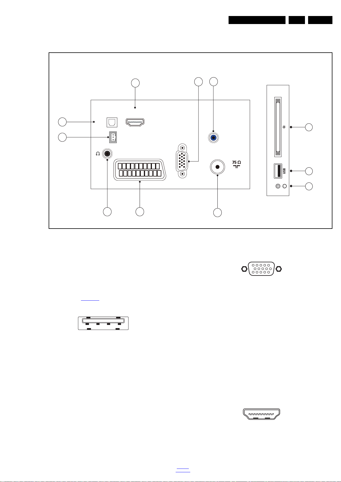
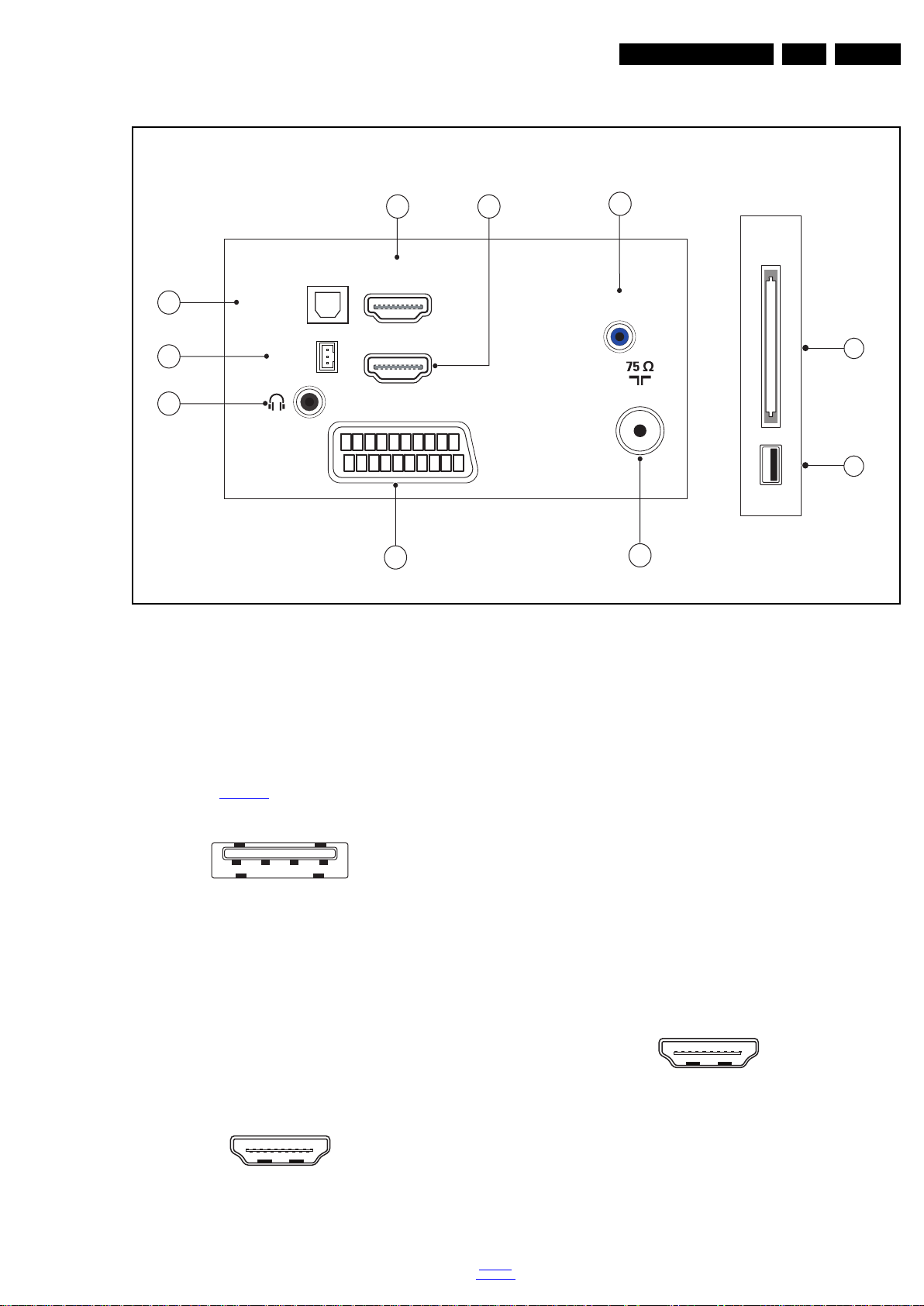
TV ANTENNA
VGA / DVI
AUDIO IN
DIGITAL
AUDIO OUT
(RGB/CVBS)
(Optional)
HDMI 1
ARC
SCART
SERV.U
VGA
19531_001_130923.eps
130923
1
2
3
4
6
5
7
8
10
9
11
Side ConnectorsRear Connectors
1 2 3 4
10000_022_090121.eps
090121
1
6
10
11
5
15
10000_002_090121.eps
090127
10000_017_090121.eps
090428
19
1
18 2
EN 5TPN14.1E LA 2.
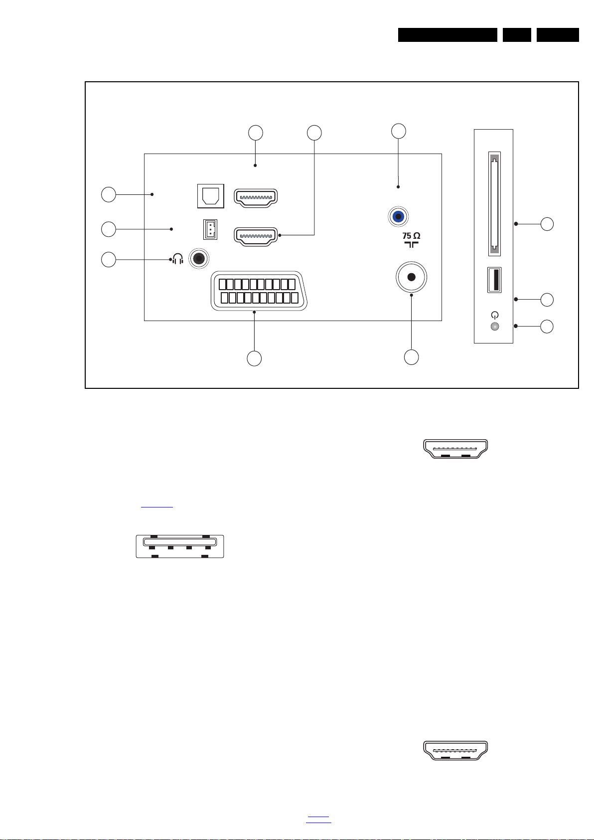
2.3 Connections ( for 2 0"/22"/24"/28"PxH4109/88 & 20"/24"PxH4109/60 & 50"Pxx4109 /88 & 24" 5210 series & 23" 4009 series)
Figure 2-1 Connection overview
Note: The following connector colour abbreviations are used
5 - PC IN:VGA
(acc. to DIN/IEC 757): Bk= Black, Bu= Blue, Gn= Green,
Gy= Grey, Rd= Red, Wh= White, Ye= Yellow.
2.3.1 Side Connections
1 - Common Interface
68p- See figure 10-13-12
2 - USB2 2.0
jk
1 -Video Red 0.7 V
2 -Video Green 0.7 V
3 -Video Blue 0.7 V
4-n.c.
5 -Ground Gnd H
Figure 2-3 VGA connector
/ 75 W j
PP
/ 75 W j
PP
/ 75 W j
PP
6 -Ground Red Gnd H
7 -Ground Green Gnd H
Figure 2-2 USB (type A)
1-+5V k
2 -Data (-) jk
3 -Data (+) jk
4 -Ground Gnd H
3 - Power Button
Turn on/off the TV.
2.3.2 Rear Connections
4 - Audio - In: Left / Right, VGA
Bu -Audio L/R in 0.5 V
/ 10 kW jq
RMS
8 -Ground Blue Gnd H
9-+5V
10 - Ground Sync Gnd H
+5 V j
DC
11 - Ground Red Gnd H
12 - DDC_SDA DDC data j
13 - H-sync 0 - 5 V j
14 - V-sync 0 - 5 V j
15 - DDC_SCL DDC clock j
6 - HDMI 1: Digital Video - In, Digital Audio with ARC In/Out
Figure 2-4 HDMI (type A) connector
1 -D2+ Data channel j
back to
div. table
2 -Shield Gnd H
2014-Nov-07
Page 6

EN 6 TPN14.1E LA2.
21
20
1
2
10000_001_090121.eps
090121
Technical Specs, Diversity, and Connections
3 -D2- Data channel j
4 -D1+ Data channel j
5-Shield Gnd H
6 -D1- Data channel j
7 -D0+ Data channel j
8-Shield Gnd H
9 -D0- Data channel j
10 - CLK+ Data channel j
11 - Shield Gnd H
12 - CLK- Data channel j
13 - Easylink/CEC Control channel jk
14 - ARC Audio Return Channel k
15 - DDC_SCL DDC clock j
16 - DDC_SDA DDC data jk
17 - Ground Gnd H
18 - +5V j
19 - HPD Hot Plug Detect j
20 - Ground Gnd H
7 - Cinch: Digital Audio - Out
BK - Coaxial 0.4 - 0.6V
/ 75 W kq
PP
8 - Service / UART
1 -Ground Gnd H
2 -UART_TX Transmit k
3 -UART_RX Receive j
9 - Head phone (Output)
Bk -Head phone 80 - 600 / 10 mW
ot
10 - EXT1: Video RGB/YC - In, CVBS - In/Out, Audio - In/Out
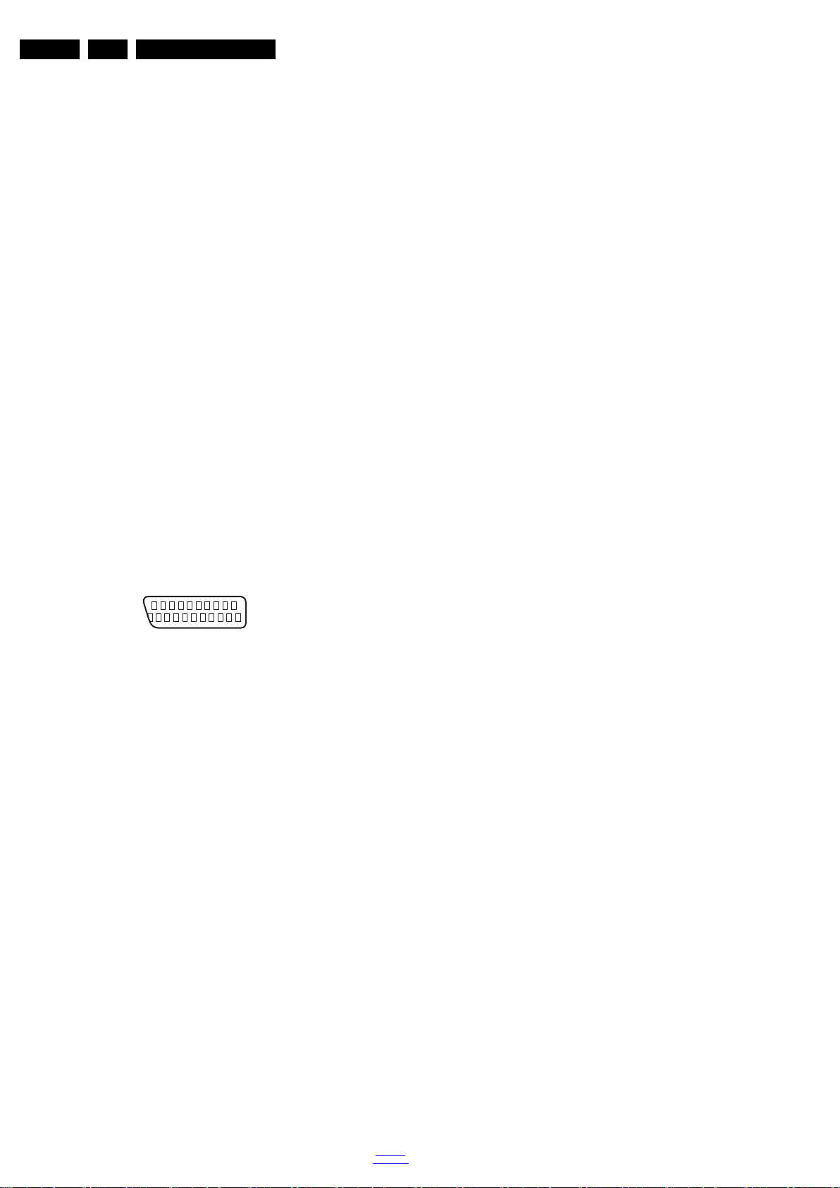
Figure 2-5 SCART connector
1 -Audio R 0.5 V
2 -Audio R 0.5 V
3 -Audio L 0.5 V
/ 1 k k
RMS
/ 10 k j
RMS
/ 1 k k
RMS
4 -Ground Audio Gnd H
5 -Ground Blue Gnd H
6 -Audio L 0.5 V
7 -Video Blue/C-out 0.7 V
8 -Function Select 0 - 2 V: INT
/ 10 k j
RMS
/ 75 jk
PP
4.5 - 7 V: EXT 16:9
9.5 - 12 V: EXT 4:3 j
9 -Ground Green Gnd H
10 - n.c.
11 - Video Green 0.7 V
12 - n.c.
/ 75 j
PP
13 - Ground Red Gnd H
14 - Ground P50 Gnd H
15 - Video Red/C 0.7 V
16 - Status/FBL 0 - 0.4 V: INT
/ 75 j
PP
1 - 3 V: EXT / 75 j
17 - Ground Video Gnd H
18 - Ground FBL Gnd H
19 - Video CVBS 1 V
20 - Video CVBS/Y 1 V
21 - Shield Gnd H
/ 75 k
PP
/ 75 j
PP
2014-Nov-07
11 - TV ANTENNA - In
Signal input from an antenna, cable or satellite.
back to
div. table
Page 7
Technical Specs, Diversity, and Connections
TV ANTENNA
VGA / DVI
SERV.U
AUDIO IN
DIGITAL
AUDIO OUT
SCART
(RGB/CVBS)
HDMI 1
ARC
VGA
SAT
19590_001_140110.eps
140110
1
2
3
4
7
6
5
8
9
11
10
12
Side ConnectorsRear Connectors
1 2 3 4
10000_022_090121.eps
090121
1
6
10
11
5
15
10000_002_090121.eps
090127
10000_017_090121.eps
090428
19
1
18 2
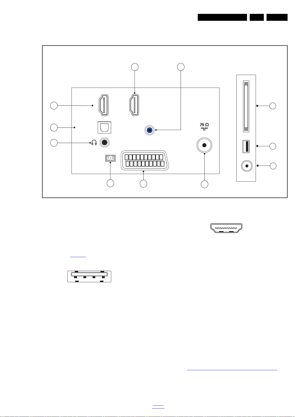
2.4 Connections ( for 22"/24"Pxx4109/12 & 22"Pxx4209/12)
EN 7TPN14.1E LA 2.
2.4.1 Side Connections
2.4.2 Rear Connections
Figure 2-6 Connection overview
Note: The following connector colour abbreviations are used
(acc. to DIN/IEC 757): Bk= Black, Bu= Blue, Gn= Green,
Gy= Grey, Rd= Red, Wh= White, Ye= Yellow.
1 - Common Interface
68p- See figure 10-13-12
jk
2 - USB2 2.0
Figure 2-7 USB (type A)
1-+5V k
2 -Data (-) jk
3 -Data (+) jk
4 -Ground Gnd H
3 - SAT - In
Signal input from an SAT.
4 - Power Button
Turn on/off the TV.
5 - TV ANTENNA - In
Signal input from an antenna, cable or satellite.
back to
div. table
6 - PC IN:VGA
Figure 2-8 VGA connector
1 -Video Red 0.7 V
2 -Video Green 0.7 V
3 -Video Blue 0.7 V
/ 75 W j
PP
/ 75 W j
PP
/ 75 W j
PP
4-n.c.
5 -Ground Gnd H
6 -Ground Red Gnd H
7 -Ground Green Gnd H
8 -Ground Blue Gnd H
9-+5V
+5 V j
DC
10 - Ground Sync Gnd H
11 - Ground Red Gnd H
12 - DDC_SDA DDC data j
13 - H-sync 0 - 5 V j
14 - V-sync 0 - 5 V j
15 - DDC_SCL DDC clock j
7 - Audio - In: Left / Right, VGA
Bu - Audio L/R in 0.5 V
/ 10 kW jq
RMS
8 - HDMI 1: Digital Video - In, Digital Audio with ARC In/Out
Figure 2-9 HDMI (type A) connector
2014-Nov-07
Page 8

EN 8 TPN14.1E LA2.
21
20
1
2
10000_001_090121.eps
090121
Technical Specs, Diversity, and Connections
1 -D2+ Data channel j
2-Shield Gnd H
3 -D2- Data channel j
4 -D1+ Data channel j
5-Shield Gnd H
6 -D1- Data channel j
7 -D0+ Data channel j
8-Shield Gnd H
9 -D0- Data channel j
10 - CLK+ Data channel j
11 - Shield Gnd H
12 - CLK- Data channel j
13 - Easylink/CEC Control channel jk
14 - ARC Audio Return Channel k
15 - DDC_SCL DDC clock j
16 - DDC_SDA DDC data jk
17 - Ground Gnd H
18 - +5V j
19 - HPD Hot Plug Detect j
20 - Ground Gnd H
9 - Cinch: Digital Audio - Out
BK - Coaxial 0.4 - 0.6V
/ 75 W kq
PP
10 - Head phone (Output)
Bk -Head phone 80 - 600 / 10 mW
ot
11 - Service / UART
1 -Ground Gnd H
2 -UART_TX Transmit k
3 -UART_RX Receive j
12 - EXT1: Video RGB/YC - In, CVBS - In/Out, Audio - In/Out
Figure 2-10 SCART connector
1 -Audio R 0.5 V
2 -Audio R 0.5 V
3 -Audio L 0.5 V
4 -Ground Audio Gnd H
/ 1 k k
RMS
/ 10 k j
RMS
/ 1 k k
RMS
5 -Ground Blue Gnd H
6 -Audio L 0.5 V
7 -Video Blue/C-out 0.7 V
/ 10 k j
RMS
/ 75 jk
PP
8 -Function Select 0 - 2 V: INT
4.5 - 7 V: EXT 16:9
9.5 - 12 V: EXT 4:3 j
9 -Ground Green Gnd H
10 - n.c.
11 - Video Green 0.7 V
/ 75 j
PP
12 - n.c.
13 - Ground Red Gnd H
14 - Ground P50 Gnd H
15 - Video Red/C 0.7 V
16 - Status/FBL 0 - 0.4 V: INT
/ 75 j
PP
1 - 3 V: EXT / 75 j
17 - Ground Video Gnd H
18 - Ground FBL Gnd H
19 - Video CVBS 1 V
20 - Video CVBS/Y 1 V
21 - Shield Gnd H
/ 75 k
PP
/ 75 j
PP
2014-Nov-07
back to
div. table
Page 9
Technical Specs, Diversity, and Connections
TV ANTENNA
SERV.U
HDMI 2
SCART (RGB/CVBS)
CI
HDMI 1
ARC
SPDIF OUT
USB
19530_001_130730.eps
130730
1
2
3
4
6
7
5
8
Side ConnectorsSide Connectors
Rear Connectors
1 2 3 4
10000_022_090121.eps
090121
10000_017_090121.eps
090428
19
1
18 2
10000_017_090121.eps
090428
19
1
18 2
2.5 Connections ( for 32" 4100 series)
EN 9TPN14.1E LA 2.
Figure 2-11 Connection overview
Note: The following connector colour abbreviations are used
(acc. to DIN/IEC 757): Bk= Black, Bu= Blue, Gn= Green,
Gy= Grey, Rd= Red, Wh= White, Ye= Yellow.
2.5.1 Side Connections
1 - Common Interface
68p- See figure 10-13-12
5 - USB2 2.0
jk
1-+5V k
2 -Data (-) jk
3 -Data (+) jk
4 -Ground Gnd H
6 - HDMI 1: Digital Video - In, Digital Audio with ARC In/Out
Figure 2-12 USB (type A)
6 -D1- Data channel j
7 -D0+ Data channel j
8 -Shield Gnd H
9 -D0- Data channel j
10 - CLK+ Data channel j
11 - Shield Gnd H
12 - CLK- Data channel j
13 - Easylink/CEC Control channel jk
14 - ARC Audio Return Channel k
15 - DDC_SCL DDC clock j
16 - DDC_SDA DDC data jk
17 - Ground Gnd H
18 - +5V j
19 - HPD Hot Plug Detect j
20 - Ground Gnd H
7 - Cinch: Digital Audio - Out
BK - Coaxial 0.4 - 0.6V
2.5.2 Rear Connections
2 - TV ANTENNA - In
Signal input from an antenna, cable or satellite.
3 - HDMI2 : Digital Video - In, Digital Audio - In/Out
/ 75 kq
PP
Figure 2-13 HDMI (type A) connector
1 -D2+ Data channel j
2-Shield Gnd H
3 -D2- Data channel j
4 -D1+ Data channel j
5-Shield Gnd H
back to
div. table
Figure 2-14 HDMI (type A) connector
1 -D2+ Data channel j
2 -Shield Gnd H
3 -D2- Data channel j
4 -D1+ Data channel j
2014-Nov-07
Page 10
EN 10 TPN14.1E LA2.
21
20
1
2
10000_001_090121.eps
090121
Technical Specs, Diversity, and Connections
5-Shield Gnd H
6 -D1- Data channel j
7 -D0+ Data channel j
8-Shield Gnd H
9 -D0- Data channel j
10 - CLK+ Data channel j
11 - Shield Gnd H
12 - CLK- Data channel j
13 - Easylink/CEC Control channel jk
14 - n.c.
15 - DDC_SCL DDC clock j
16 - DDC_SDA DDC data jk
17 - Ground Gnd H
18 - +5V j
19 - HPD Hot Plug Detect j
20 - Ground Gnd H
4 - Service / UART
1 -Ground Gnd H
2 -UART_TX Transmit k
3 -UART_RX Receive j
8 - EXT1: Video RGB/YC - In, CVBS - In/Out, Audio - In/Out
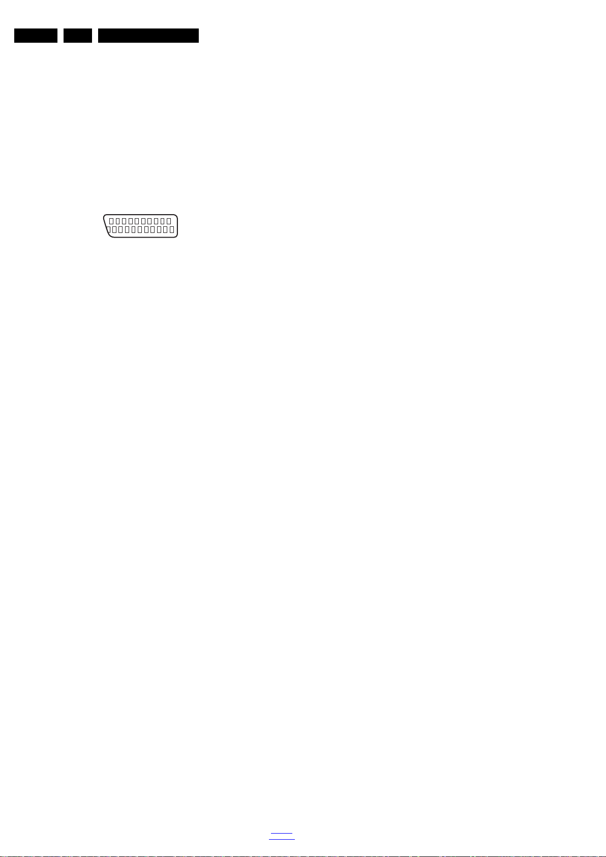
Figure 2-15 SCART connector
1 -Audio R 0.5 V
2 -Audio R 0.5 V
3 -Audio L 0.5 V
4 -Ground Audio Gnd H
/ 1 k k
RMS
/ 10 k j
RMS
/ 1 k k
RMS
5 -Ground Blue Gnd H
6 -Audio L 0.5 V
7 -Video Blue/C-out 0.7 V
8 -Function Select 0 - 2 V: INT
/ 10 k j
RMS
/ 75 jk
PP
4.5 - 7 V: EXT 16:9
9.5 - 12 V: EXT 4:3 j
9 -Ground Green Gnd H
10 - n.c.
11 - Video Green 0.7 V
12 - n.c.
/ 75 j
PP
13 - Ground Red Gnd H
14 - Ground P50 Gnd H
15 - Video Red/C 0.7 V
/ 75 j
PP
16 - Status/FBL 0 - 0.4 V: INT
1 - 3 V: EXT / 75 j
17 - Ground Video Gnd H
18 - Ground FBL Gnd H
19 - Video CVBS 1 V
20 - Video CVBS/Y 1 V
/ 75 k
PP
/ 75 j
PP
21 - Shield Gnd H
2014-Nov-07
back to
div. table
Page 11
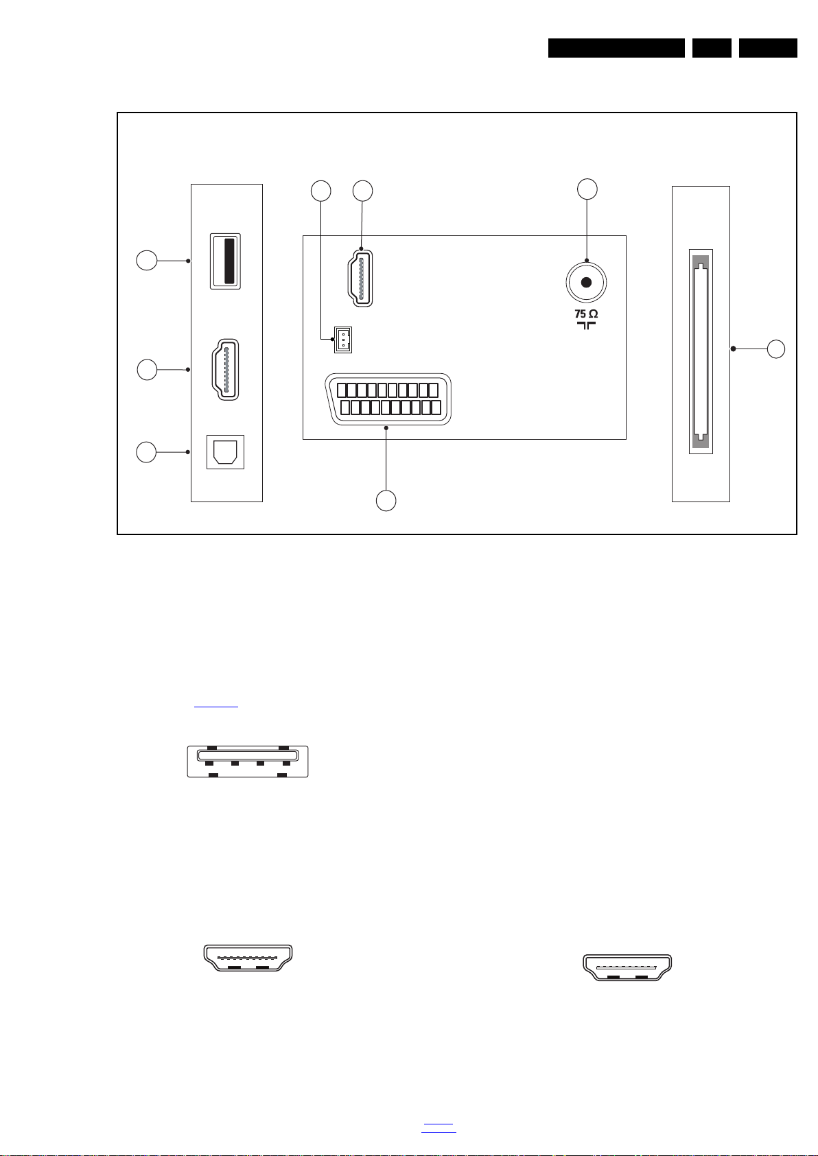
Technical Specs, Diversity, and Connections
CI
USB
TV ANTENNA
SERV.U
HDMI 2
HDMI 1
ARC
SCART (RGB/CVBS)
DIGITAL
AUDIO OUT
AUDIO IN
DVI
19530_002_130719.eps
130719
1
2
3
5 4
6
7
8
9
10
Side ConnectorsRear Connectors
1 2 3 4
10000_022_090121.eps
090121
10000_017_090121.eps
090428
19
1
18 2
10000_017_090121.eps
090428
19
1
18 2
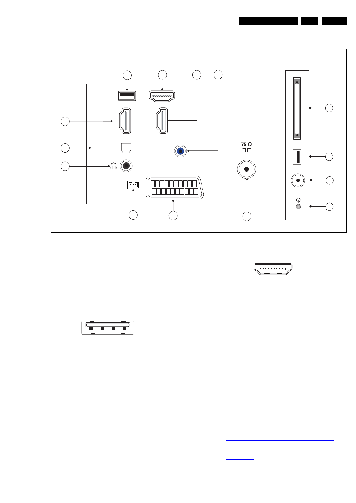
2.6 Connections ( for 40" & 47"PFx 4109/88 & 55"Pxx5109/88)
EN 11TPN14.1E LA 2.
2.6.1 Side Connections
2.6.2 Rear Connections
Figure 2-16 Connection overview
Note: The following connector colour abbreviations are used
(acc. to DIN/IEC 757): Bk= Black, Bu= Blue, Gn= Green,
Gy= Grey, Rd= Red, Wh= White, Ye= Yellow.
1 - Common Interface
68p- See figure 10-13-12
jk
2 - USB2 2.0
Figure 2-17 USB (type A)
1-+5V k
2 -Data (-) jk
3 -Data (+) jk
4 -Ground Gnd H
3 - Audio - In: Left / Right, VGA
Bu - Audio L/R in 0.5 V
4 - HDMI2 : Digital Video - In, Digital Audio - In/Out
Figure 2-18 HDMI (type A) connector
/ 10 kW jq
RMS
back to
div. table
1 -D2+ Data channel j
2 -Shield Gnd H
3 -D2- Data channel j
4 -D1+ Data channel j
5 -Shield Gnd H
6 -D1- Data channel j
7 -D0+ Data channel j
8 -Shield Gnd H
9 -D0- Data channel j
10 - CLK+ Data channel j
11 - Shield Gnd H
12 - CLK- Data channel j
13 - Easylink/CEC Control channel jk
14 - n.c.
15 - DDC_SCL DDC clock j
16 - DDC_SDA DDC data jk
17 - Ground Gnd H
18 - +5V j
19 - HPD Hot Plug Detect j
20 - Ground Gnd H
5 - HDMI 1: Digital Video - In, Digital Audio with ARC In/Out
Figure 2-19 HDMI (type A) connector
1 -D2+ Data channel j
2 -Shield Gnd H
3 -D2- Data channel j
4 -D1+ Data channel j
5 -Shield Gnd H
6 -D1- Data channel j
7 -D0+ Data channel j
2014-Nov-07
Page 12
EN 12 TPN14.1E LA2.
21
20
1
2
10000_001_090121.eps
090121
Technical Specs, Diversity, and Connections
8-Shield Gnd H
9 -D0- Data channel j
10 - CLK+ Data channel j
11 - Shield Gnd H
12 - CLK- Data channel j
13 - Easylink/CEC Control channel jk
14 - ARC Audio Return Channel k
15 - DDC_SCL DDC clock j
16 - DDC_SDA DDC data jk
17 - Ground Gnd H
18 - +5V j
19 - HPD Hot Plug Detect j
20 - Ground Gnd H
6 - Cinch: Digital Audio - Out
BK - Coaxial 0.4 - 0.6V
/ 75 W kq
PP
7 - Service / UART
1 -Ground Gnd H
2 -UART_TX Transmit k
3 -UART_RX Receive j
8 - Head phone (Output)
Bk -Head phone 80 - 600 / 10 mW
ot
9 - EXT1: Video RGB/YC - In, CVBS - In/Out, Audio - In/Out
Figure 2-20 SCART connector
1 -Audio R 0.5 V
2 -Audio R 0.5 V
3 -Audio L 0.5 V
4 -Ground Audio Gnd H
/ 1 k k
RMS
/ 10 k j
RMS
/ 1 k k
RMS
5 -Ground Blue Gnd H
6 -Audio L 0.5 V
7 -Video Blue/C-out 0.7 V
8 -Function Select 0 - 2 V: INT
/ 10 k j
RMS
/ 75 jk
PP
4.5 - 7 V: EXT 16:9
9.5 - 12 V: EXT 4:3 j
9 -Ground Green Gnd H
10 - n.c.
11 - Video Green 0.7 V
12 - n.c.
/ 75 j
PP
13 - Ground Red Gnd H
14 - Ground P50 Gnd H
15 - Video Red/C 0.7 V
/ 75 j
PP
16 - Status/FBL 0 - 0.4 V: INT
1 - 3 V: EXT / 75 j
17 - Ground Video Gnd H
18 - Ground FBL Gnd H
19 - Video CVBS 1 V
20 - Video CVBS/Y 1 V
/ 75 k
PP
/ 75 j
PP
21 - Shield Gnd H
2014-Nov-07
10 - TV ANTENNA - In
Signal input from an antenna, cable or satellite.
back to
div. table
Page 13
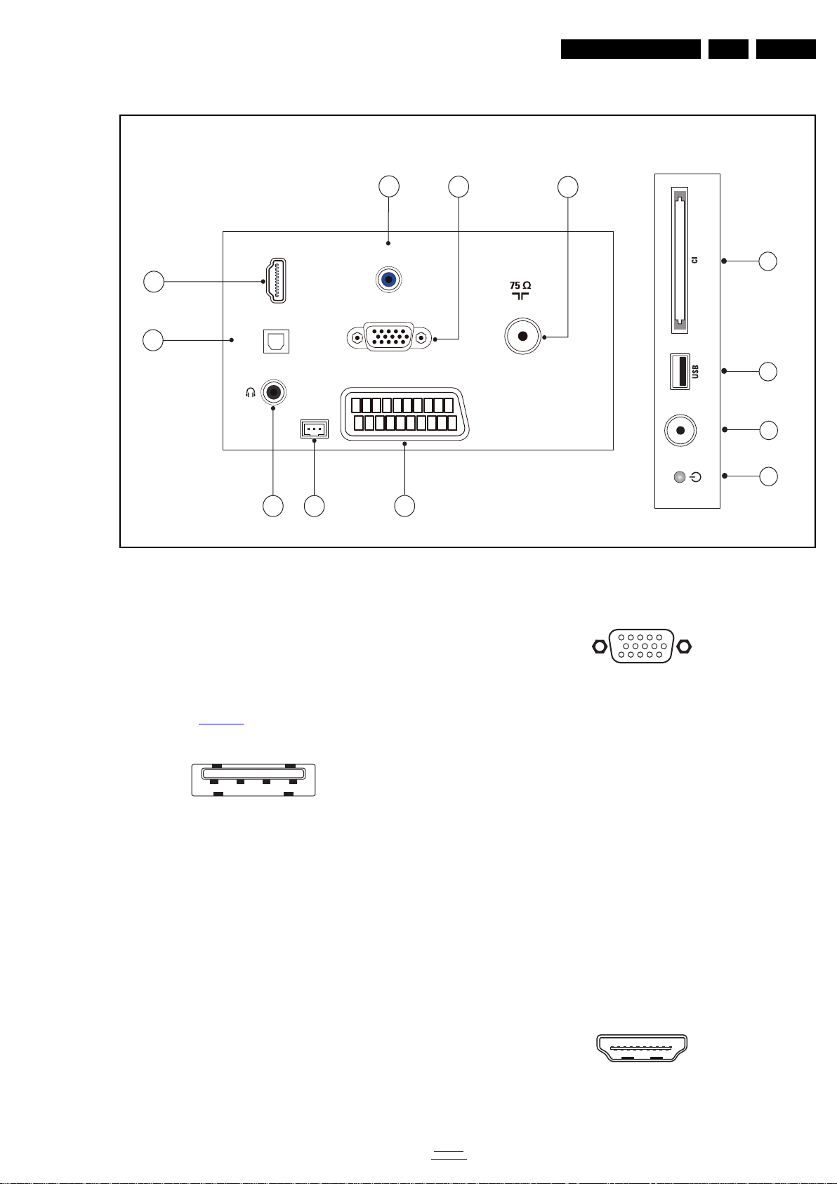
Technical Specs, Diversity, and Connections
CI
USB2
TV ANTENNA
SERV.U
HDMI 3
HDMI 2
HDMI 1
ARC
SCART (RGB/CVBS)
DIGITAL
AUDIO OUT
AUDIO IN
DVI
SAT
USB1
19591_001.eps
1
2
3
4
7
8
5
6
9
10
11
13
12
14
Side ConnectorsRear Connectors
1 2 3 4
10000_022_090121.eps
090121
10000_017_090121.eps
090428
19
1
18 2
2.7 Connections ( for 40" & 47"PFT4109/12 & 50"Pxx4109/12)
EN 13TPN14.1E LA 2.
Figure 2-21 Connection overview
Note: The following connector colour abbreviations are used
(acc. to DIN/IEC 757): Bk= Black, Bu= Blue, Gn= Green,
Gy= Grey, Rd= Red, Wh= White, Ye= Yellow.
2.7.1 Side Connections
1 - Common Interface
68p- See figure 10-13-12
2 - USB2 2.0
Figure 2-22 USB (type A)
1-+5V k
2 -Data (-) jk
3 -Data (+) jk
4 -Ground Gnd H
3 - SAT - In
Signal input from an SAT.
4 - Power Button
Turn on/off the TV.
2.7.2 Rear Connections
5 - Audio - In: Left / Right, VGA
Bu - Audio L/R in 0.5 V
jk
/ 10 kW jq
RMS
6 - HDMI3 : Digital Video - In, Digital Audio - In/Out
Figure 2-23 HDMI (type A) connector
1 -D2+ Data channel j
2 -Shield Gnd H
3 -D2- Data channel j
4 -D1+ Data channel j
5 -Shield Gnd H
6 -D1- Data channel j
7 -D0+ Data channel j
8 -Shield Gnd H
9 -D0- Data channel j
10 - CLK+ Data channel j
11 - Shield Gnd H
12 - CLK- Data channel j
13 - Easylink/CEC Control channel jk
14 - n.c.
15 - DDC_SCL DDC clock j
16 - DDC_SDA DDC data jk
17 - Ground Gnd H
18 - +5V j
19 - HPD Hot Plug Detect j
20 - Ground Gnd H
7 - HDMI 1: Digital Video - In, Digital Audio - In/Out
See 6 - HDMI3 : Digital Video - In, Digital Audio - In/Out
8 - USB1 2.0
See 2 - USB2 2.0
back to
div. table
9 - HDMI 2 : Digital Video - In, Digital Audio - In/Out
See 6 - HDMI3 : Digital Video - In, Digital Audio - In/Out
2014-Nov-07
Page 14
EN 14 TPN14.1E LA2.
21
20
1
2
10000_001_090121.eps
090121
Technical Specs, Diversity, and Connections
10 - Cinch: Digital Audio - Out
BK - Coaxial 0.4 - 0.6V
/ 75 W kq
PP
11 - Head phone (Output)
Bk -Head phone 80 - 600 / 10 mW
ot
12 - Service / UART
1 -Ground Gnd H
2 -UART_TX Transmit k
3 -UART_RX Receive j
13 - EXT1: Video RGB/YC - In, CVBS - In/Out, Audio - In/Out
Figure 2-24 SCART connector
1 -Audio R 0.5 V
2 -Audio R 0.5 V
3 -Audio L 0.5 V
/ 1 k k
RMS
/ 10 k j
RMS
/ 1 k k
RMS
4 -Ground Audio Gnd H
5 -Ground Blue Gnd H
6 -Audio L 0.5 V
7 -Video Blue/C-out 0.7 V
8 -Function Select 0 - 2 V: INT
/ 10 k j
RMS
/ 75 jk
PP
4.5 - 7 V: EXT 16:9
9.5 - 12 V: EXT 4:3 j
9 -Ground Green Gnd H
10 - n.c.
11 - Video Green 0.7 V
12 - n.c.
/ 75 j
PP
13 - Ground Red Gnd H
14 - Ground P50 Gnd H
15 - Video Red/C 0.7 V
16 - Status/FBL 0 - 0.4 V: INT
/ 75 j
PP
1 - 3 V: EXT / 75 j
17 - Ground Video Gnd H
18 - Ground FBL Gnd H
19 - Video CVBS 1 V
20 - Video CVBS/Y 1 V
21 - Shield Gnd H
/ 75 k
PP
/ 75 j
PP
14 - TV ANTENNA - In
Signal input from an antenna, cable or satellite.
2014-Nov-07
back to
div. table
Page 15
Technical Specs, Diversity, and Connections
CI
USB
TV ANTENNA
SERV.U
HDMI 2
HDMI 1
ARC
SCART (RGB/CVBS)
(optional)
DIGITAL
AUDIO OUT
AUDIO IN
DVI
19593_001.eps
1
2
3
4
6 5
7
8
9
10
11
Side ConnectorsRear Connectors
1 2 3 4
10000_022_090121.eps
090121
10000_017_090121.eps
090428
19
1
18 2
10000_017_090121.eps
090428
19
1
18 2
2.8 Connections ( for 32" & 40" & 50" 4009/4300 series)
EN 15TPN14.1E LA 2.
Figure 2-25 Connection overview
Note: The following connector colour abbreviations are used
6 - HDMI2 : Digital Video - In, Digital Audio - In/Out
(acc. to DIN/IEC 757): Bk= Black, Bu= Blue, Gn= Green,
Gy= Grey, Rd= Red, Wh= White, Ye= Yellow.
2.8.1 Side Connections
1 - Common Interface
68p- See figure 10-13-12
2 - USB2 2.0
jk
Figure 2-27 HDMI (type A) connector
1 -D2+ Data channel j
2 -Shield Gnd H
3 -D2- Data channel j
4 -D1+ Data channel j
5 -Shield Gnd H
6 -D1- Data channel j
7 -D0+ Data channel j
8 -Shield Gnd H
9 -D0- Data channel j
Figure 2-26 USB (type A)
10 - CLK+ Data channel j
1-+5V k
2 -Data (-) jk
3 -Data (+) jk
4 -Ground Gnd H
3 - SAT - In
Signal input from an SAT.
4 - Power Button
Turn on/off the TV.
2.8.2 Rear Connections
5 - Audio - In: Left / Right, VGA
Bu - Audio L/R in 0.5 V
/ 10 kW jq
RMS
11 - Shield Gnd H
12 - CLK- Data channel j
13 - Easylink/CEC Control channel jk
14 - n.c.
15 - DDC_SCL DDC clock j
16 - DDC_SDA DDC data jk
17 - Ground Gnd H
18 - +5V j
19 - HPD Hot Plug Detect j
20 - Ground Gnd H
7 - HDMI 1: Digital Video - In, Digital Audio with ARC In/Out
back to
div. table
Figure 2-28 HDMI (type A) connector
2014-Nov-07
Page 16
EN 16 TPN14.1E LA2.
21
20
1
2
10000_001_090121.eps
090121
Technical Specs, Diversity, and Connections
1 -D2+ Data channel j
2-Shield Gnd H
3 -D2- Data channel j
4 -D1+ Data channel j
5-Shield Gnd H
6 -D1- Data channel j
7 -D0+ Data channel j
8-Shield Gnd H
9 -D0- Data channel j
10 - CLK+ Data channel j
11 - Shield Gnd H
12 - CLK- Data channel j
13 - Easylink/CEC Control channel jk
14 - ARC Audio Return Channel k
15 - DDC_SCL DDC clock j
16 - DDC_SDA DDC data jk
17 - Ground Gnd H
18 - +5V j
19 - HPD Hot Plug Detect j
20 - Ground Gnd H
8 - Cinch: Digital Audio - Out
BK - Coaxial 0.4 - 0.6V
/ 75 W kq
PP
9 - Service / UART
1 -Ground Gnd H
2 -UART_TX Transmit k
3 -UART_RX Receive j
10 - Head phone (Output)
Bk -Head phone 80 - 600 W / 10 mW
ot
11 - EXT1: Video RGB/YC - In, CVBS - In/Out, Audio - In/Out
Figure 2-29 SCART connector
1 -Audio R 0.5 V
2 -Audio R 0.5 V
3 -Audio L 0.5 V
4 -Ground Audio Gnd H
/ 1 k k
RMS
/ 10 k j
RMS
/ 1 k k
RMS
5 -Ground Blue Gnd H
6 -Audio L 0.5 V
7 -Video Blue/C-out 0.7 V
/ 10 k j
RMS
/ 75 jk
PP
8 -Function Select 0 - 2 V: INT
4.5 - 7 V: EXT 16:9
9.5 - 12 V: EXT 4:3 j
9 -Ground Green Gnd H
10 - n.c.
11 - Video Green 0.7 V
/ 75 j
PP
12 - n.c.
13 - Ground Red Gnd H
14 - Ground P50 Gnd H
15 - Video Red/C 0.7 V
16 - Status/FBL 0 - 0.4 V: INT
/ 75 j
PP
1 - 3 V: EXT / 75 j
17 - Ground Video Gnd H
18 - Ground FBL Gnd H
19 - Video CVBS 1 V
20 - Video CVBS/Y 1 V
21 - Shield Gnd H
/ 75 k
PP
/ 75 j
PP
2014-Nov-07
12 - TV ANTENNA - In
Signal input from an antenna, cable or satellite.8
back to
div. table
Page 17
Technical Specs, Diversity, and Connections
CI
USB2
TV ANTENNA
SERV.U
HDMI 3
HDMI 2
SCART (RGB/CVBS)
DIGITAL
AUDIO OUT
AUDIO IN
DVI
SAT
19593_002.eps
1
2
3
5
4
6
7
8
10
9
11
Side ConnectorsRear Connectors
(optionalȑ
1 2 3 4
10000_022_090121.eps
090121
10000_017_090121.eps
090428
19
1
18 2
EN 17TPN14.1E LA 2.
2.9 Connections ( for 32" & 40" & 48" & 55" 5100 series & 42"/47"/55" 5190 & 5200 series & 32"/40"/50" 4009 series)
Figure 2-30 Connection overview
Note: The following connector colour abbreviations are used
(acc. to DIN/IEC 757): Bk= Black, Bu= Blue, Gn= Green,
Gy= Grey, Rd= Red, Wh= White, Ye= Yellow.
2.9.1 Side Connections
1 - Common Interface
68p- See figure 10-13-12
2 - USB2 2.0
Figure 2-31 USB (type A)
1-+5V k
2 -Data (-) jk
3 -Data (+) jk
4 -Ground Gnd H
3 - SAT - In
Signal input from an SAT.
4 - Power Button
Turn on/off the TV.
2.9.2 Rear Connections
5 - Audio - In: Left / Right, VGA
Bu - Audio L/R in 0.5 V
jk
/ 10 kW jq
RMS
6 - HDMI 3 : Digital Video - In, Digital Audio - In/Out
Figure 2-32 HDMI (type A) connector
1 -D2+ Data channel j
2 -Shield Gnd H
3 -D2- Data channel j
4 -D1+ Data channel j
5 -Shield Gnd H
6 -D1- Data channel j
7 -D0+ Data channel j
8 -Shield Gnd H
9 -D0- Data channel j
10 - CLK+ Data channel j
11 - Shield Gnd H
12 - CLK- Data channel j
13 - Easylink/CEC Control channel jk
14 - n.c.
15 - DDC_SCL DDC clock j
16 - DDC_SDA DDC data jk
17 - Ground Gnd H
18 - +5V j
19 - HPD Hot Plug Detect j
20 - Ground Gnd
7 - HDMI 2: Digital Video - In, Digital Audio - In/Out
See 6 - HDMI3 : Digital Video - In, Digital Audio - In/Out
8 - Cinch: Digital Audio - Out
BK - Coaxial 0.4 - 0.6V
/ 75 W kq
PP
back to
div. table
2014-Nov-07
Page 18

EN 18 TPN14.1E LA2.
21
20
1
2
10000_001_090121.eps
090121
Technical Specs, Diversity, and Connections
9 - Head phone (Output)
Bk -Head phone 80 - 600 / 10 mW
ot
10 - Service / UART
1 -Ground Gnd H
2 -UART_TX Transmit k
3 -UART_RX Receive j
11 - EXT1: Video RGB/YC - In, CVBS - In/Out, Audio - In/Out
Figure 2-33 SCART connector
1 -Audio R 0.5 V
2 -Audio R 0.5 V
3 -Audio L 0.5 V
4 -Ground Audio Gnd H
/ 1 k k
RMS
/ 10 k j
RMS
/ 1 k k
RMS
2.10 Chassis Overview
Refer to 9. Block Diagrams for PWB/CBA locations.6
5 -Ground Blue Gnd H
6 -Audio L 0.5 V
7 -Video Blue/C-out 0.7 V
8 -Function Select 0 - 2 V: INT
/ 10 k j
RMS
/ 75 jk
PP
4.5 - 7 V: EXT 16:9
9.5 - 12 V: EXT 4:3 j
9 -Ground Green Gnd H
10 - n.c.
11 - Video Green 0.7 V
12 - n.c.
/ 75 j
PP
13 - Ground Red Gnd H
14 - Ground P50 Gnd H
15 - Video Red/C 0.7 V
16 - Status/FBL 0 - 0.4 V: INT
/ 75 j
PP
1 - 3 V: EXT / 75 j
17 - Ground Video Gnd H
18 - Ground FBL Gnd H
19 - Video CVBS 1 V
20 - Video CVBS/Y 1 V
21 - Shield Gnd H
/ 75 k
PP
/ 75 j
PP
12 - TV ANTENNA - In
Signal input from an antenna, cable or satellite.
2014-Nov-07
back to
div. table
Page 19

Precautions, Notes, and Abbreviation List
3. Precautions, Notes, and Abbreviation List
Index of this chapter:
3.1 Safety Instructions
3.2 Warnings
3.3 Notes
3.4 Abbreviation List
3.1 Safety Instructions
Safety regulations require the following during a repair:
• Connect the set to the Mains/AC Power via an isolation
transformer (> 800 VA).
• Replace safety components, indicated by the symbol h,
only by components identical to the original ones. Any
other component substitution (other than original type) may
increase risk of fire or electrical shock hazard.
Safety regulations require that after a repair, the set must be
returned in its original condition. Pay in particular attention to
the following points:
• Route the wire trees correctly and fix them with the
mounted cable clamps.
• Check the insulation of the Mains/AC Power lead for
external damage.
• Check the strain relief of the Mains/AC Power cord for
proper function.
• Check the electrical DC resistance between the Mains/AC
Power plug and the secondary side (only for sets that have
a Mains/AC Power isolated power supply):
1. Unplug the Mains/AC Power cord and connect a wire
between the two pins of the Mains/AC Power plug.
2. Set the Mains/AC Power switch to the “on” position
(keep the Mains/AC Power cord unplugged!).
3. Measure the resistance value between the pins of the
Mains/AC Power plug and the metal shielding of the
tuner or the aerial connection on the set. The reading
should be between 4.5 M and 12 M.
4. Switch “off” the set, and remove the wire between the
two pins of the Mains/AC Power plug.
• Check the cabinet for defects, to prevent touching of any
inner parts by the customer.
3.2 Warnings
• All ICs and many other semiconductors are susceptible to
electrostatic discharges (ESD w). Careless handling
during repair can reduce life drastically. Make sure that,
during repair, you are connected with the same potential as
the mass of the set by a wristband with resistance. Keep
components and tools also at this same potential.
• Be careful during measurements in the high voltage
section.
• Never replace modules or other components while the unit
is switched “on”.
• When you align the set, use plastic rather than metal tools.
This will prevent any short circuits and the danger of a
circuit becoming unstable.
3.3 Notes
3.3.1 General
• Measure the voltages and waveforms with regard to the
chassis (= tuner) ground (H), or hot ground (I), depending
on the tested area of circuitry. The voltages and waveforms
shown in the diagrams are indicative. Measure them in the
Service Default Mode with a colour bar signal and stereo
sound (L: 3 kHz, R: 1 kHz unless stated otherwise) and
picture carrier at 475.25 MHz for PAL, or 61.25 MHz for
NTSC (channel 3).
• Where necessary, measure the waveforms and voltages
with (D) and without (E) aerial signal. Measure the
voltages in the power supply section both in normal
operation (G) and in stand-by (F). These values are
indicated by means of the appropriate symbols.
3.3.2 Schematic Notes
• All resistor values are in ohms, and the value multiplier is
often used to indicate the decimal point location (e.g. 2K2
indicates 2.2 k).
• Resistor values with no multiplier may be indicated with
either an “E” or an “R” (e.g. 220E or 220R indicates 220 ).
• All capacitor values are given in micro-farads (10
nano-farads (n 10
• Capacitor values may also use the value multiplier as the
decimal point indication (e.g. 2p2 indicates 2.2 pF).
• An “asterisk” (*) indicates component usage varies. Refer
to the diversity tables for the correct values.
• The correct component values are listed on the Philips
Spare Parts Web Portal.
3.3.3 Spare Parts
For the latest spare part overview, consult your Philips Spare
Part web portal.
3.3.4 BGA (Ball Grid Array) ICs
Introduction
For more information on how to handle BGA devices, visit this
URL: http://www.atyourservice-magazine.com
“Magazine”, then go to “Repair downloads”. Here you will find
Information on how to deal with BGA-ICs.
BGA Temperature Profiles
For BGA-ICs, you must use the correct temperature-profile.
Where applicable and available, this profile is added to the IC
Data Sheet information section in this manual.
3.3.5 Lead-free Soldering
Due to lead-free technology some rules have to be respected
by the workshop during a repair:
• Use only lead-free soldering tin. If lead-free solder paste is
required, please contact the manufacturer of your soldering
equipment. In general, use of solder paste within
workshops should be avoided because paste is not easy to
store and to handle.
• Use only adequate solder tools applicable for lead-free
soldering tin. The solder tool must be able:
– To reach a solder-tip temperature of at least 400°C.
– To stabilize the adjusted temperature at the solder-tip.
– To exchange solder-tips for different applications.
• Adjust your solder tool so that a temperature of around
360°C - 380°C is reached and stabilized at the solder joint.
Heating time of the solder-joint should not exceed ~ 4 sec.
Avoid temperatures above 400°C, otherwise wear-out of
tips will increase drastically and flux-fluid will be destroyed.
To avoid wear-out of tips, switch “off” unused equipment or
reduce heat.
• Mix of lead-free soldering tin/parts with leaded soldering
tin/parts is possible but PHILIPS recommends strongly to
avoid mixed regimes. If this cannot be avoided, carefully
clear the solder-joint from old tin and re-solder with new tin.
3.3.6 Alternative BOM identification
It should be noted that on the European Service website,
“Alternative BOM” is referred to as “Design variant”.
The third digit in the serial number (example:
AG2B0335000001) indicates the number of the alternative
B.O.M. (Bill Of Materials) that has been used for producing the
specific TV set. In general, it is possible that the same TV
model on the market is produced with e.g. two different types
of displays, coming from two different suppliers. This will then
back to
div. table
-9
), or pico-farads (p 10
. Select
EN 19TPN14.1E LA 3.
-6
),
-12
).
2014-Nov-07
Page 20
EN 20 TPN14.1E LA3.
10000_053_110228.eps
110228
Precautions, Notes, and Abbreviation List
result in sets which have the same CTN (Commercial Type
Number; e.g. 28PW9515/12) but which have a different B.O.M.
number.
By looking at the third digit of the serial number, one can
identify which B.O.M. is used for the TV set he is working with.
If the third digit of the serial number contains the number “1”
(example: AG1B033500001), then the TV set has been
manufactured according to B.O.M. number 1. If the third digit is
a “2” (example: AG2B0335000001), then the set has been
produced according to B.O.M. no. 2. This is important for
ordering the correct spare parts!
For the third digit, the numbers 1...9 and the characters A...Z
can be used, so in total: 9 plus 26= 35 different B.O.M.s can be
indicated by the third digit of the serial number.
Identification: The bottom line of a type plate gives a 14-digit
serial number. Digits 1 and 2 refer to the production centre (e.g.
SN is Lysomice, RJ is Kobierzyce), digit 3 refers to the B.O.M.
code, digit 4 refers to the Service version change code, digits 5
and 6 refer to the production year, and digits 7 and 8 refer to
production week (in example below it is 2010 week 10 / 2010
week 17). The 6 last digits contain the serial number.
Figure 3-1 Serial number (example)
3.3.7 Board Level Repair (BLR) or Component Level Repair (CLR)
If a board is defective, consult your repair procedure to decide
if the board has to be exchanged or if it should be repaired on
component level.
If your repair procedure says the board should be exchanged
completely, do not solder on the defective board. Otherwise, it
cannot be returned to the O.E.M. supplier for back charging!
3.3.8 Practical Service Precautions
• It makes sense to avoid exposure to electrical shock.
While some sources are expected to have a possible
dangerous impact, others of quite high potential are of
limited current and are sometimes held in less regard.
• Always respect voltages. While some may not be
dangerous in themselves, they can cause unexpected
reactions that are best avoided. Before reaching into a
powered TV set, it is best to test the high voltage insulation.
It is easy to do, and is a good service precaution.
3.4 Abbreviation List
0/6/12 SCART switch control signal on A/V
board. 0 = loop through (AUX to TV),
6 = play 16 : 9 format, 12 = play 4 : 3
format
AARA Automatic Aspect Ratio Adaptation:
algorithm that adapts aspect ratio to
remove horizontal black bars; keeps
the original aspect ratio
ACI Automatic Channel Installation:
algorithm that installs TV channels
directly from a cable network by
means of a predefined TXT page
ADC Analogue to Digital Converter
AFC Automatic Frequency Control: control
signal used to tune to the correct
frequency
AGC Automatic Gain Control: algorithm that
controls the video input of the feature
box
AM Amplitude Modulation
AP Asia Pacific
AR Aspect Ratio: 4 by 3 or 16 by 9
ASF Auto Screen Fit: algorithm that adapts
aspect ratio to remove horizontal black
bars without discarding video
information
ATSC Advanced Television Systems
Committee, the digital TV standard in
the USA
ATV See Auto TV
Auto TV A hardware and software control
system that measures picture content,
and adapts image parameters in a
dynamic way
AV External Audio Video
AVC Audio Video Controller
AVIP Audio Video Input Processor
B/G Monochrome TV system. Sound
carrier distance is 5.5 MHz
BDS Business Display Solutions (iTV)
BLR Board-Level Repair
BTSC Broadcast Television Standard
Committee. Multiplex FM stereo sound
system, originating from the USA and
used e.g. in LATAM and AP-NTSC
countries
B-TXT Blue TeleteXT
C Centre channel (audio)
CEC Consumer Electronics Control bus:
remote control bus on HDMI
connections
CL Constant Level: audio output to
connect with an external amplifier
CLR Component Level Repair
ComPair Computer aided rePair
CP Connected Planet / Copy Protection
CSM Customer Service Mode
CTI Color Transient Improvement:
manipulates steepness of chroma
transients
CVBS Composite Video Blanking and
Synchronization
DAC Digital to Analogue Converter
DBE Dynamic Bass Enhancement: extra
low frequency amplification
DCM Data Communication Module. Also
referred to as System Card or
Smartcard (for iTV).
DDC See “E-DDC”
D/K Monochrome TV system. Sound
carrier distance is 6.5 MHz
DFI Dynamic Frame Insertion
DFU Directions For Use: owner's manual
DMR Digital Media Reader: card reader
DMSD Digital Multi Standard Decoding
DNM Digital Natural Motion
2014-Nov-07
back to
div. table
Page 21

Precautions, Notes, and Abbreviation List
EN 21TPN14.1E LA 3.
DNR Digital Noise Reduction: noise
reduction feature of the set
DRAM Dynamic RAM
DRM Digital Rights Management
DSP Digital Signal Processing
DST Dealer Service Tool: special remote
control designed for service
technicians
DTCP Digital Transmission Content
Protection; A protocol for protecting
digital audio/video content that is
traversing a high speed serial bus,
such as IEEE-1394
DVB-C Digital Video Broadcast - Cable
DVB-T Digital Video Broadcast - Terrestrial
DVD Digital Versatile Disc
DVI(-d) Digital Visual Interface (d= digital only)
E-DDC Enhanced Display Data Channel
(VESA standard for communication
channel and display). Using E-DDC,
the video source can read the EDID
information form the display.
EDID Extended Display Identification Data
(VESA standard)
EEPROM Electrically Erasable and
Programmable Read Only Memory
EMI Electro Magnetic Interference
EPG Electronic Program Guide
EPLD Erasable Programmable Logic Device
EU Europe
EXT EXTernal (source), entering the set by
SCART or by cinches (jacks)
FDS Full Dual Screen (same as FDW)
FDW Full Dual Window (same as FDS)
FLASH FLASH memory
FM Field Memory or Frequency
Modulation
FPGA Field-Programmable Gate Array
FTV Flat TeleVision
Gb/s Giga bits per second
G-TXT Green TeleteXT
H H_sync to the module
HD High Definition
HDD Hard Disk Drive
HDCP High-bandwidth Digital Content
Protection: A “key” encoded into the
HDMI/DVI signal that prevents video
data piracy. If a source is HDCP coded
and connected via HDMI/DVI without
the proper HDCP decoding, the
picture is put into a “snow vision” mode
or changed to a low resolution. For
normal content distribution the source
and the display device must be
enabled for HDCP “software key”
decoding.
HDMI High Definition Multimedia Interface
HP HeadPhone
I Monochrome TV system. Sound
2
C Inter IC bus
I
2
I
D Inter IC Data bus
2
S Inter IC Sound bus
I
carrier distance is 6.0 MHz
IF Intermediate F requency
IR Infra Red
IRQ Interrupt Request
ITU-656 The ITU Radio communication Sector
(ITU-R) is a standards body
subcommittee of the International
Telecommunication Union relating to
radio communication. ITU-656 (a.k.a.
SDI), is a digitized video format used
for broadcast grade video.
Uncompressed digital component or
digital composite signals can be used.
back to
div. table
The SDI signal is self-synchronizing,
uses 8 bit or 10 bit data words, and has
a maximum data rate of 270 Mbit/s,
with a minimum bandwidth of 135
MHz.
iTV Institutional TeleVision; TV sets for
hotels, hospitals etc.
LS Last Status; The settings last chosen
by the customer and read and stored
in RAM or in the NVM. They are called
at start-up of the set to configure it
according to the customer's
preferences
LATAM Latin America
LCD Liquid Crystal Display
LED Light Emitting Diode
L/L' Monochrome TV system. Sound
carrier distance is 6.5 MHz. L' is Band
I, L is all bands except for Band I
LPL LG.Philips LCD (supplier)
LS Loudspeaker
LVDS Low Voltage Differential Signalling
Mbps Mega bits per second
M/N Monochrome TV system. Sound
carrier distance is 4.5 MHz
MHEG Part of a set of international standards
related to the presentation of
multimedia information, standardised
by the Multimedia and Hypermedia
Experts Group. It is commonly used as
a language to describe interactive
television services
MIPS Microprocessor without Interlocked
Pipeline-Stages; A RISC-based
microprocessor
MOP Matrix Output Processor
MOSFET Metal Oxide Silicon Field Effect
Transistor, switching device
MPEG Motion Pictures Experts Group
MPIF Multi Platform InterFace
MUTE MUTE Line
MTV Mainstream TV: TV-mode with
Consumer TV features enabled (iTV)
NC Not Connected
NICAM Near Instantaneous Compounded
Audio Multiplexing. This is a digital
sound system, mainly used in Europe.
NTC Negative Temperature Coefficient,
non-linear resistor
NTSC National Television Standard
Committee. Color system mainly used
in North America and Japan. Color
carrier NTSC M/N= 3.579545 MHz,
NTSC 4.43= 4.433619 MHz (this is a
VCR norm, it is not transmitted off-air)
NVM Non-Volatile Memory: IC containing
TV related data such as alignments
O/C Open Circuit
OSD On Screen Display
OAD Over the Air Download. Method of
software upgrade via RF transmission.
Upgrade software is broadcasted in
TS with TV channels.
OTC On screen display Teletext and
Control; also called Artistic (SAA5800)
P50 Project 50: communication protocol
between TV and peripherals
PAL Phase Alternating Line. Color system
mainly used in West Europe (colour
carrier = 4.433619 MHz) and South
America (colour carrier
PAL M = 3.575612 MHz and
PAL N = 3.582056 MHz)
PCB Printed Circuit Board (same as “PWB”)
PCM Pulse Code Modulation
2014-Nov-07
Page 22

EN 22 TPN14.1E LA3.
Precautions, Notes, and Abbreviation List
PDP Plasma Display Panel
PFC Power Factor Corrector (or
Pre-conditioner)
PIP Picture In Picture
PLL Phase Locked Loop. Used for e.g.
FST tuning systems. The customer
can give directly the desired frequency
POD Point Of Deployment: a removable
CAM module, implementing the CA
system for a host (e.g. a TV-set)
POR Power On Reset, signal to reset the uP
PSDL Power Supply for Direct view LED
backlight with 2D-dimming
PSL Power Supply with integrated LED
drivers
PSLS Power Supply with integrated LED
drivers with added Scanning
functionality
PTC Positive Temperature Coefficient,
non-linear resistor
PWB Printed Wiring Board (same as “PCB”)
PWM Pulse Width Modulation
QRC Quasi Resonant Converter
QTNR Quality Temporal Noise Reduction
QVCP Quality Video Composition Processor
RAM Random Access Memory
RGB Red, Green, and Blue. The primary
color signals for TV. By mixing levels
of R, G, and B, all colors (Y/C) are
reproduced.
RC Remote Control
RC5 / RC6 Signal protocol from the remote
control receiver
RESET RESET signal
ROM Read Only Memory
RSDS Reduced Swing Differential Signalling
data interface
R-TXT Red TeleteXT
SAM Service Alignment Mode
S/C Short Circuit
SCART Syndicat des Constructeurs
d'Appareils Radiorécepteurs et
SCL Serial Clock I
Téléviseurs
SCL-F CLock Signal on Fast I
SD Standard Definition
SDA Serial Data I
SDA-F DAta Signal on Fast I
2
C
2
C bus
2
C
2
C bus
SDI Serial Digital Interface, see “ITU-656”
SDRAM Synchronous DRAM
SECAM SEequence Couleur Avec Mémoire.
Colour system mainly used in France
and East Europe. Colour
carriers = 4.406250 MHz and
4.250000 MHz
SIF Sound Intermediate Frequency
SMPS Switched Mode Power Supply
SoC System on Chip
SOG Sync On Green
SOPS Self Oscillating Power Supply
SPI Serial Peripheral Interface bus; a
4-wire synchronous serial data link
standard
S/PDIF Sony Philips Digital InterFace
SRAM Static RAM
SRP Service Reference Protocol
SSB Small Signal Board
SSC Spread Spectrum Clocking, used to
reduce the effects of EMI
STB Set Top Box
STBY STand-BY
SVGA 800 × 600 (4:3)
SVHS Super Video Home System
SW Software
SWAN Spatial temporal Weighted Averaging
Noise reduction
SXGA 1280 × 1024
TFT Thin Film Transistor
THD Total Harmonic Distortion
TMDS Transmission Minimized Differential
Signalling
TS Transport Stream
TXT TeleteXT
TXT-DW Dual Window with TeleteXT
UI User Interface
uP Microprocessor
UXGA 1600 × 1200 (4:3)
V V-sync to the module
VESA Video Electronics Standards
Association
VGA 640 × 480 (4:3)
VL Variable Level out: processed audio
output toward external amplifier
VSB Vestigial Side Band; modulation
method
WYSIWYR What You See Is What You Record:
record selection that follows main
picture and sound
WXGA 1280 × 768 (15:9)
XTAL Quartz crystal
XGA 1024 × 768 (4:3)
Y Luminance signal
Y/C Luminance (Y) and Chrominance (C)
signal
YPbPr Component video. Luminance and
scaled color difference signals (B-Y
and R-Y)
YUV Component video
2014-Nov-07
back to
div. table
Page 23
4. Mechanical Instructions
19590_100_140107.eps
140107
CN601
CN401
CN9904
CN701
CN408
MAIN POWER SUPPLY
(1054)
A
IR/LED BOARD
(1056)
J
SSB
(1053)
B
ECN701
ECN601
ECN408
ECN401
ECN601
ECN601
LOUDSPEAKER
(1184)
LOUDSPEAKER
(1184)
CN201
CN8101
Index of this chapter:
4.1 Cable Dressing
4.2 Service Positions
4.3 Assembly/Panel Removal ( for 20"/22"/24"/28" 4100 series
& 22" 4209 series & 32" 4300 series & 23" 4009 series)
4.4 Assembly/Panel Removal ( for 32" 4100 series)
4.5 Assembly/Panel Removal ( for 40"/47"/50" 4100 series &
40" 4300 series)
4.6 Assembly/Panel Removal ( for 24" 5200 series)
4.7 Assembly/Panel Removal ( for 40"/55" 5100 series)
4.8 Assembly/Panel Removal ( for 32"/48" 5100 series)
4.1 Cable Dressing
Mechanical Instructions
4.9 Assembly/Panel Removal ( for 42"/47"/55" 5190 & 5200
series)
4.10 Assembly/Panel Removal ( for 50" 4300 series)
4.11 Assembly/Panel Removal ( for 32"/40"/50" 4009 series)
4.12 Set Re-assembly
Notes:
• Figures below can deviate slightly from the actual situation,
due to the different set executions.
EN 23TPN14.1E LA 4.
Figure 4-1 Cable dressing (22" 4100 series)
back to
div. table
2014-Nov-07
Page 24
EN 24 TPN14.1E LA4.
19598_100.eps
CN401
CN601
CN701
CN801
CN408
MAIN POWER SUPPLY
(1055)
A
SSB
(1053)
B
ECN701
ECN601
ECN408
ECN401
ECN401
ECN601
LOUDSPEAKER
(1184)
LOUDSPEAKER
(1184)
CN805
IR/LED BOARD
(1056)
J
19595_100.eps
CN401
CN701
CN9904
CN409
MAIN POWER SUPPLY
(1054)
A
SSB
(1053)
B
ECN701
ECN409
ECN601
ECN409
ECN401
ECN601
CN8101
IR/LED BOARD
(1056)
J
LOUDSPEAKER
(1184)
LOUDSPEAKER
(1184)
CN601
Mechanical Instructions
2014-Nov-07
Figure 4-2 Cable dressing (22" 4200 series)
Figure 4-3 Cable dressing ( 23" PHx4009/88 series)
back to
div. table
Page 25
Mechanical Instructions
19595_101.eps
CN601
CN701
CN9904
CN409
MAIN POWER SUPPLY
(1054)
A
SSB
(1053)
B
ECN701
ECN409
ECN601
ECN409
ECN401
ECN601
CN8101
IR/LED BOARD
(1056)
J
LOUDSPEAKER
(1184)
LOUDSPEAKER
(1184)
CN401
19590_101_140109.eps
140109
CN401
CN9904
CN701
CN408
CN601
MAIN POWER SUPPLY
(1054)
A
IR/LED BOARD
(1056)
J
SSB
(1053)
B
ECN701
ECN601
ECN408
ECN601
ECN401
LOUDSPEAKER
(1184)
LOUDSPEAKER
(1184)
CN201
CN8101
EN 25TPN14.1E LA 4.
Figure 4-4 Cable dressing ( 23" PHx4009/12 series)
Figure 4-5 Cable dressing (24" 4100 series)
back to
div. table
2014-Nov-07
Page 26
EN 26 TPN14.1E LA4.
19593_100.eps
CN401
CN701
CN9903
CN409
MAIN POWER SUPPLY
(1054)
A
SSB
(1053)
B
ECN401
ECN701
ECN601
ECN409
ECN401
ECN601
CN8101
IR/LED BOARD
(1056)
J
LOUDSPEAKER
(1185)
LOUDSPEAKER
(1187)
CN601
19593_101.eps
CN401
CN701
CN9903
CN408
MAIN POWER SUPPLY
(1054)
A
SSB
(1053)
B
ECN401
ECN701
ECN601
ECN408
ECN401
ECN601
CN8101
IR/LED BOARD
(1056)
J
LOUDSPEAKER
(1187)
CN601
LOUDSPEAKER
(1185)
Mechanical Instructions
Figure 4-6 Cable dressing (24" Pxx5219/88 series)
2014-Nov-07
Figure 4-7 Cable dressing (24" Pxx5219/12 series)
back to
div. table
Page 27
Mechanical Instructions
19594_100.eps
CN401
CN701
CN9101
CN409
MAIN POWER SUPPLY
(1054)
A
SSB
(1053)
B
ECN701
ECN601
ECN409
ECN401
ECN601
CN8101
IR/LED BOARD
(1056)
J
LOUDSPEAKER
(1184)
LOUDSPEAKER
(1184)
CN601
19597_100.eps
CN601
CN401
CN9101
CN8602
CN701
CN408
MAIN POWER SUPPLY
(1054)
A
IR/LED BOARD
(1056)
J
SSB
(1053)
B
ECN701
ECN601
ECN408
ECN401
ECN601
LOUDSPEAKER
(1184)
LOUDSPEAKER
(1184)
CN201
EN 27TPN14.1E LA 4.
Figure 4-8 Cable dressing (28" 4100 series)
Figure 4-9 Cable dressing (32PFH4009 series)
back to
div. table
2014-Nov-07
Page 28
EN 28 TPN14.1E LA4.
19597_101.eps
CN401
CN601
CN9101
CN8602
CN701
CN408
MAIN POWER SUPPLY
(1054)
A
IR/LED BOARD
(1056)
J
SSB
(1053)
B
ECN701
ECN601
ECN408
ECN401
ECN401
ECN601
LOUDSPEAKER
(1184)
LOUDSPEAKER
(1184)
CN201
19597_102.eps
CN401
CN701
CN9101
CN8604
CN601
CN408
MAIN POWER SUPPLY
(1054)
A
IR/LED BOARD
(1056)
J
SSB
(1053)
B
ECN701
ECN601
ECN601
ECN401
ECN408
ECN408
ECN401
ECN601
LOUDSPEAKER
(1184)
LOUDSPEAKER
(1184)
CN201
Mechanical Instructions
Figure 4-10 Cable dressing (32PFK/T4009 series)
2014-Nov-07
Figure 4-11 Cable dressing (32PHH4009 series)
div. table
back to
Page 29

Mechanical Instructions
19597_103.eps
CN601
CN701
CN9101
CN8604
CN401
CN408
MAIN POWER SUPPLY
(1054)
A
IR/LED BOARD
(1056)
J
SSB
(1053)
B
ECN701
ECN601
ECN408
ECN401
ECN601
LOUDSPEAKER
(1184)
LOUDSPEAKER
(1184)
CN201
19590_102_140109.eps
140109
CN4501
CN601
CN8101
CN4101
Control Board IR/LED penal
(1066)
EJ
SSB+PSU combination panel
(1052)
BA
ECN8101
ECN601
ECN601
ECN4101
ECN4501
LOUDSPEAKER
(1184)
LOUDSPEAKER
(1184)
CN201
EN 29TPN14.1E LA 4.
Figure 4-12 Cable dressing (32PHK/T4009 series)
Figure 4-13 Cable dressing (32" 4100 series)
back to
div. table
2014-Nov-07
Page 30

EN 30 TPN14.1E LA4.
19593_102.eps
CN601
CN401
CN701
CN8101
CN409
MAIN POWER SUPPLY
(1054)
A
SSB
(1053)
B
ECN701
ECN601
ECN409
ECN401
ECN601
ECN601
LOUDSPEAKER
(1184)
LOUDSPEAKER
(1184)
CN9101
IR/LED BOARD
(1056)
J
19593_103.eps
CN401
CN701
CN8101
CN408
CN601
MAIN POWER SUPPLY
(1054)
A
SSB
(1053)
B
ECN701
ECN601
ECN408
ECN401
ECN601
LOUDSPEAKER
(1184)
LOUDSPEAKER
(1184)
CN9101
IR/LED BOARD
(1056)
J
Mechanical Instructions
Figure 4-14 Cable dressing (32" PHx4309/88 series)
2014-Nov-07
Figure 4-15 Cable dressing (32" PHx4309/12 series)
back to
div. table
Page 31

Mechanical Instructions
19594_101.eps
CN401
CN701
CN8501
CN409
MAIN POWER SUPPLY
(1054)
A
SSB
(1053)
B
ECN701
ECN601
ECN409
ECN401
ECN601
CN9101
IR/LED BOARD
(1056)
J
LOUDSPEAKER
(1184)
LOUDSPEAKER
(1184)
CN601
19595_102.eps
CN601
CN701
CN9904
CN409
MAIN POWER SUPPLY
(1054)
A
SSB
(1053)
B
ECN701
ECN601
ECN409
ECN401
ECN601
CN8101
IR/LED BOARD
(1056)
J
LOUDSPEAKER
(1184)
LOUDSPEAKER
(1184)
CN401
EN 31TPN14.1E LA 4.
Figure 4-16 Cable dressing (32" PFx4309/88 series)
Figure 4-17 Cable dressing (32" PFx4309/12 series)
back to
div. table
2014-Nov-07
Page 32

EN 32 TPN14.1E LA4.
19593_104.eps
CN401
CN701
CN8501
CN408
CN601
MAIN POWER SUPPLY
(1054)
A
SSB
(1053)
B
ECN701
ECN601
ECN408
ECN401
ECN401
ECN601
LOUDSPEAKER
(1185)
LOUDSPEAKER
(1186)
CN9101
IR/LED BOARD
(1056)
J
KEYBOARD CONTROL
(1057)
E
CN01
19590_103_140110.eps
140110
CN401
CN601
CN8501
CN408
CN701
CN9101
SSB
(1053)
B
ECN601
ECN601
ECN408
ECN401
LOUDSPEAKER
(1184)
LOUDSPEAKER
(1184)
MAIN POWER SUPPLY
(1054)
A
ECN701
Control Board IR/LED penal
(1066)
CN201
EJ
Mechanical Instructions
Figure 4-18 Cable dressing (32" 5100 series)
2014-Nov-07
Figure 4-19 Cable dressing ( 40" & 47" PFx4109/88 series)
back to
div. table
Page 33

Mechanical Instructions
19597_104.eps
CN401
CN601
CN701
CN9101
CN8601
CN408
MAIN POWER SUPPLY
(1054)
A
IR/LED BOARD
(1056)
J
SSB
(1053)
B
ECN701
ECN601
ECN408
ECN401
ECN601
LOUDSPEAKER
(1184)
LOUDSPEAKER
(1184)
CN201
19597_105.eps
CN601
CN401 CN701
CN9101
CN8601
CN408
MAIN POWER SUPPLY
(1054)
A
IR/LED BOARD
(1056)
J
SSB
(1053)
B
ECN701
ECN601
ECN408
ECN401
ECN601
LOUDSPEAKER
(1184)
LOUDSPEAKER
(1184)
CN201
EN 33TPN14.1E LA 4.
Figure 4-20 Cable dressing ( 40PFH4009 series)
Figure 4-21 Cable dressing ( 40PFK/T4009 series)
div. table
back to
2014-Nov-07
Page 34

EN 34 TPN14.1E LA4.
19591_100.eps
CN401
CN601
CN701
CN9101
CN409
MAIN POWER SUPPLY
(1054)
A
Control Board IR/LED panel
(1066)
EJ
SSB
(1053)
B
ECN701
ECN601
ECN409
ECN401
ECN601
LOUDSPEAKER
(1184)
LOUDSPEAKER
(1184)
CN201
CN8501
19593_105.eps
CN601
CN401
CN701
CN8101 CN9101
CN409
MAIN POWER SUPPLY
(1054)
A
SSB
(1053)
B
ECN701
ECN601
ECN409
ECN401
ECN601
ECN601
LOUDSPEAKER
(1184)
LOUDSPEAKER
(1184)
IR/LED BOARD
(1056)
J
Mechanical Instructions
Figure 4-22 Cable dressing ( 40" & 47" PFx4109/12 series)
2014-Nov-07
Figure 4-23 Cable dressing ( 40" Pxx4300/88 series)
back to
div. table
Page 35

Mechanical Instructions
19593_106.eps
CN401
CN601
CN701
CN8101 CN9101
CN408
MAIN POWER SUPPLY
(1054)
A
SSB
(1053)
B
ECN701
ECN601
ECN408
ECN401
ECN601
LOUDSPEAKER
(1184)
LOUDSPEAKER
(1184)
IR/LED BOARD
(1056)
J
19593_107.eps
CN401
CN601
CN701
CN8101
CN9301
CN408
MAIN POWER SUPPLY
(1054)
A
SSB
(1053)
B
ECN701
ECN408
ECN401
ECN601
ECN601
ECN401
LOUDSPEAKER
(1185)
LOUDSPEAKER
(1186)
IR/LED BOARD
(1056)
J
KEYBOARD CONTROL
(1057)
E
CN01
EN 35TPN14.1E LA 4.
Figure 4-24 Cable dressing ( 40" Pxx4300/12 series)
back to
div. table
Figure 4-25 Cable dressing ( 40" 5100 series)
2014-Nov-07
Page 36

EN 36 TPN14.1E LA4.
19594_102.eps
CN700
CN1404
CN9102 CN9101
CN408
CN601
MAIN POWER SUPPLY
(1054)
A
SSB
(1053)
B
ECN700
ECN601
ECN408
ECN401
ECN401
ECN601
IR/LED BOARD
(1056)
J
LOUDSPEAKER
(1186)
LOUDSPEAKER
(1185)
CN401
KEYBOARD CONTROL
(1057)
E
CN01
AmbiLight
AL
(1062)
AmbiLight
AL
(1063)
EXA03
ECN1404
ECN9102
19594_103.eps
CN700 CN1404
CN9101
CN9301
CN408
CN601
MAIN POWER SUPPLY
(1054)
A
SSB
(1053)
B
ECN700
ECN9101
ECN601
ECN408
ECN401
ECN401
ECN601
IR/LED BOARD
(1056)
J
LOUDSPEAKER
(1186)
LOUDSPEAKER
(1185)
CN401
KEYBOARD CONTROL
(1057)
E
CN01
AmbiLight
AL
(1062)
AmbiLight
AL
(1063)
EXA03
ECN1404
Mechanical Instructions
2014-Nov-07
Figure 4-26 Cable dressing ( 42" 5190 & 5200 series)
Figure 4-27 Cable dressing ( 47" 5190 & 5200 series)
back to
div. table
Page 37

Mechanical Instructions
19593_108.eps
CN601
CN401
CN701
CN8101 CN8101
CN408
MAIN POWER SUPPLY
(1054)
A
SSB
(1053)
B
ECN701
ECN401
ECN601
ECN601
ECN408
ECN401
LOUDSPEAKER
(1185)
LOUDSPEAKER
(1186)
KEYBOARD CONTROL
(1057)
E
CN01
IR/LED BOARD
(1056)
J
19597_106.eps
CN701
CN601
CN401
CN8101
CN9301
CN408
MAIN POWER SUPPLY
(1054)
A
IR/LED BOARD
(1056)
J
SSB
(1053)
B
ECN701
ECN401
ECN408
ECN408
ECN601
ECN601
LOUDSPEAKER
(1184)
LOUDSPEAKER
(1184)
CN201
EN 37TPN14.1E LA 4.
Figure 4-28 Cable dressing ( 48" 5100 series)
back to
div. table
2014-Nov-07
Figure 4-29 Cable dressing ( 50PFH4009 series)
Page 38

EN 38 TPN14.1E LA4.
19597_107.eps
CN601
CN701CN401
CN8101
CN9301
CN408
MAIN POWER SUPPLY
(1054)
A
IR/LED BOARD
(1056)
J
SSB
(1053)
B
ECN701
ECN401
ECN401
ECN408
ECN408
ECN601
ECN601
LOUDSPEAKER
(1184)
LOUDSPEAKER
(1184)
CN201
19592_101.eps
CN401
CN601
CN701
CN8101
CN409
MAIN POWER SUPPLY
(1054)
A
SSB
(1053)
B
ECN701
ECN601
ECN409
ECN401
ECN601
ECN401
LOUDSPEAKER
(1184)
LOUDSPEAKER
(1184)
CN9301
Control Board IR/LED panel
(1066)
EJ
CN201
Mechanical Instructions
Figure 4-30 Cable dressing ( 50PFK/T4009 series)
2014-Nov-07
Figure 4-31 Cable dressing ( 50" PFx4109/12 series)
back to
div. table
Page 39

Mechanical Instructions
19592_102.eps
CN601
CN401
CN701
CN8101
CN408
MAIN POWER SUPPLY
(1054)
A
SSB
(1053)
B
ECN601
ECN408
ECN401
ECN601
ECN701
ECN401
LOUDSPEAKER
(1184)
LOUDSPEAKER
(1184)
CN9301
Control Board IR/LED panel
(1066)
EJ
CN201
19592_102.eps
CN601
CN401
CN701
CN8101
CN408
MAIN POWER SUPPLY
(1054)
A
SSB
(1053)
B
ECN601
ECN408
ECN401
ECN601
ECN701
ECN401
LOUDSPEAKER
(1184)
LOUDSPEAKER
(1184)
CN9301
Control Board IR/LED panel
(1066)
EJ
CN201
EN 39TPN14.1E LA 4.
Figure 4-32 Cable dressing ( 50" PFx4109/88 series)
Figure 4-33 Cable dressing ( 50" 4300 series)
back to
div. table
2014-Nov-07
Page 40

EN 40 TPN14.1E LA4.
19593_109.eps
CN601
CN401
CN701
CN8101
CN9301
CN408
MAIN POWER SUPPLY
(1054)
A
SSB
(1053)
B
ECN701
ECN408
ECN401
ECN601
ECN601
ECN401
LOUDSPEAKER
(1184)
LOUDSPEAKER
(1184)
KEYBOARD CONTROL
(1057)
E
CN01
IR/LED BOARD
(1056)
J
19593_110.eps
CN401
CN601
CN701
CN8101
CN9301
CN409
MAIN POWER SUPPLY
(1054)
A
SSB
(1053)
B
ECN701
ECN409
ECN601
ECN601
ECN401
ECN401
LOUDSPEAKER
(1184)
LOUDSPEAKER
(1184)
KEYBOARD CONTROL
(1057)
E
CN01
IR/LED BOARD
(1056)
J
Mechanical Instructions
Figure 4-34 Cable dressing ( 55" PFx5100/88 series)
2014-Nov-07
Figure 4-35 Cable dressing ( 55" PFx5100/12 series)
back to
div. table
Page 41

Mechanical Instructions
19594_104.eps
CN700
CN1404
CN9101
CN9301
CN408
CN601
MAIN POWER SUPPLY
(1054)
A
SSB
(1053)
B
ECN700
ECN9101
ECN601
ECN408
ECN401
ECN401
ECN601
IR/LED BOARD
(1056)
J
LOUDSPEAKER
(1186)
LOUDSPEAKER
(1185)
CN401
KEYBOARD CONTROL
(1057)
E
CN01
AmbiLight
AL
(1062)
AmbiLight
AL
(1063)
EXA03
ECN1404
EN 41TPN14.1E LA 4.
Figure 4-36 Cable dressing ( 55" 5190 & 5200 series)
back to
div. table
2014-Nov-07
Page 42

EN 42 TPN14.1E LA4.
19590_104_140111.eps
140111
1
Q4 × 25
Q3 × 8
1
1
2
2
2
3
3
Mechanical Instructions
4.2 Service Positions
For easy servicing of a TV set, the set should be put face down
on a soft flat surface, foam buffers or other specific workshop
tools. Ensure that a stable situation is created to perform
measurements and alignments. When using foam bars take
care that these always support the cabinet and never only the
display. Caution: Failure to follow these guidelines can
seriously damage the display!
Ensure that ESD safe measures are taken.
4.3 Assembly/Panel Re moval ( for 20"/2 2"/24"/28" 4100 series & 22" 4209 series & 32" 4300 series & 23" 4009 series)
Instructions below apply to the 24PFT4109/12, but will be
similar for 20"/22"/24"/28" 4100 series & 22" 4209 series & 32"
4300 series & 23" 4009 series models.
4.3.1 Rear Cover
Refer to Figure 4-37
Warning: Disconnect the mains power cord before removing
the rear cover.
1. Remove fixation screws [1] that secure the base assy, pull
out the base assy from the set. Then remove the fixation
screws [2] that secure the rear cover. Refer to Figure 4-37
for details.
2. At the indicated areas [3] the cover is secured by clips. Be
very careful with releasing those.
3. Gently lift the rear cover from the TV. Make sure that wires
and cables are not damaged while lifting the rear cover
from the set.
for details.
4.3.2 Small Signal Board (SSB)
Refer to Figure 4-38
Caution: it is mandatory to remount all different screws at their
original position during re-assembly. Failure to do so may result
in damaging the SSB.
1. Release the clips from the LVDS [1] connector that connect
with the SSB.
Caution: be careful, as these are very fragile connectors!
2. Unplug all other connectors [2].
3. Remove all the fixation screws [3] from the SSB.
4. The SSB can now be shifted from side connector cover,
then lifted and taken out of the I/O bracket.Refer to
Figure 4-38
for details.
for details.
2014-Nov-07
Figure 4-37 Rear cover removal
back to
div. table
Page 43

Mechanical Instructions
19590_105_140111.eps
140111
2
1
3
3
3
3
4.4.1 Rear Cover
EN 43TPN14.1E LA 4.
Figure 4-38 SSB removal
4.3.3 Power Supply Unit (PSU)
Caution: it is mandatory to remount all different screws at their
original position during re-assembly. Failure to do so may result
in damaging the PSU.
1. Gently unplug all connectors from the PSU.
2. Remove all fixation screws from the PSU.
3. The PSU can be taken out of the set now.
Refer to Figure 4-39
Warning: Disconnect the mains power cord before removing
the rear cover.
1. Remove fixation screws [1] that secure the base assy, pull
out the base assy from the set. Then remove the fixation
screws [2], [3] that secure the rear cover. Refer to
Figure 4-39
2. Gently lift the rear cover from the TV. Make sure that wires
and cables are not damaged while lifting the rear cover
from the set.
for details.
for details.
4.3.4 Speakers
1. Gently release the tapes that secures the speaker cables.
2. Unplug the speaker connectors from the SSB.
3. Take the speakers out.
When defective, replace the both units.
4.3.5 Stand bracket
1. Remove all fixation screws of the bracket.
2. Lift the bracket from the set.
4.3.6 IR/LED panel
1. Remove the stand bracket, as described earlier.
2. Unplug the connector from the IR/LED panel.
3. Gently release the clip that holds the panel and take it out
from the bezel.
When defective, replace the whole unit.
4.3.7 LCD Panel
1. Remove the SSB as described earlier.
2. Remove the PSU as described earlier.
3. Remove the stand bracket as described earlier.
4. Remove the IR/LED as described earlier.
5. Remove the fixations screws that fix the metal clamps to
the front bezel. Take out those clamps.
6. Remove all other metal parts not belonging to the panel.
7. Lift the LCD Panel from the bezel.
When defective, replace the whole unit.
4.4 Assembly/Panel Removal ( for 32" 4100 series)
Instructions below apply to the 32PHH4109/88, but will be
similar for other 32" 4100 series models.
back to
div. table
2014-Nov-07
Page 44

EN 44 TPN14.1E LA4.
19590_106_140111.eps
140111
1
M4 × 10
Q3 × 8
1
1
1
1
2
2
2
2
2
2
2
M3 × 6
3
3
3
19590_107_140111.eps
140111
Q3 × 8
1
1
1
Mechanical Instructions
Figure 4-39 Rear cover removal [1]
2014-Nov-07
Figure 4-40 Rear cover removal [2]
back to
div. table
Page 45

Mechanical Instructions
19590_108_140111.eps
140111
1
1
1
1
19590_109_140111.eps
140111
2
3
1
4
4
4
4
EN 45TPN14.1E LA 4.
4.4.2 Speakers
Refer toFigure 4-40
1. Remove fixation screws [1] that secure the speakers cover,
Refer to Figure 4-40
and Figure 4-41 for details.
for details.
2. Gently lift the speakers cover from the TV. Make sure that
wires and cables are not damaged while lifting the rear
cover from the set.
3. Remove the fixation screws [1] that secure the speakers.
Refer to Figure 4-41
4. Gently take the speakers out.
When defective, replace the whole unit.
for details.
4.4.3 Small Signal Board (SSB) + PSU combination panel
Refer to Figure 4-42
Caution: it is mandatory to remount all different screws at their
original position during re-assembly. Failure to do so may result
in damaging the SSB + PSU combination panel.
1. Release the clips from the LVDS connector that connect
with the SSB + PSU combination panel [1].
Caution: be careful, as these are very fragile connectors!
2. Unplug all other connectors [2] , [3].
3. Remove all the fixation screws [4] from the SSB + PSU
combination panel.
4. The SSB + PSU combination panel can now be shifted
from side connector cover, then lifted and taken out of the
I/O bracket. Refer to Figure 4-42
for details.
for details.
Figure 4-41 Speakers removal
Figure 4-42 SSB + PSU combination panel removal
back to
div. table
2014-Nov-07
Page 46

EN 46 TPN14.1E LA4.
19590_110_140111.eps
14011
1
M4 × 10
Q3 × 8
1
1
1
1
2
2
2
2
2
2
2
2
2
2
2
2
2
M3 × 6
3
3
Mechanical Instructions
4.4.4 Stand bracket
1. Remove all fixation screws of the bracket.
2. Lift the bracket from the set.
4.4.5 Control Board IR/LED Panel
1. Remove the stand bracket, as described earlier.
2. Unplug the connector from the Control Board IR/LED
panel.
3. Gently release the clip that holds the panel and take it out
from the bezel.
When defective, replace the whole unit.
4.4.6 LCD Panel
1. Remove the SSB + PSU combination panelas described
earlier.
2. Remove the stand bracket as described earlier.
3. Remove the Control Board IR/LED panel as described
earlier.
4. Remove the fixations screws that fix the metal clamps to
the front bezel. Take out those clamps.
5. Remove all other metal parts not belonging to the panel.
6. Lift the LCD Panel from the bezel.
When defective, replace the whole unit.
4.5 Assembly/Panel Removal ( for 40"/47"/50" 4100 series & 40" 4300 series)
Instructions below apply to the 40PFH4109/88. but will be
similar for other 40"/47"/50" 4100 & 40" 4300 series models.
4.5.1 Rear Cover
Refer to Figure 4-43
Warning: Disconnect the mains power cord before removing
the rear cover.
1. Remove fixation screws [1] that secure the base assy, pull
out the base assy from the set. Then remove the fixation
screws [2], [3] that secure the rear cover. Refer to
Figure 4-43
2. Gently lift the rear cover from the TV. Make sure that wires
and cables are not damaged while lifting the rear cover
from the set.
for details.
for details.
2014-Nov-07
Figure 4-43 Rear cover removal [1]
back to
div. table
Page 47

Mechanical Instructions
19590_111_140111.eps
140111
Q3 × 8
1
1
1
1 1
1
1
19590_112_140111.eps
14011
EN 47TPN14.1E LA 4.
Figure 4-44 Rear cover removal [2]
Figure 4-45 Speakers removal
back to
div. table
2014-Nov-07
Page 48

EN 48 TPN14.1E LA4.
19590_113_140111.eps
140111
2
1
3
3
3
3
Mechanical Instructions
4.5.2 Speakers
Refer to Figure 4-44
1. Remove fixation screws [1] that secure the speakers cover,
Refer to Figure 4-44
2. Gently lift the speakers cover from the TV. Make sure that
wires and cables are not damaged while lifting the rear
cover from the set.
3. Remove the fixation screws [1] that secure the speakers.
Refer to Figure 4-45
4. Gently take the speakers out.
When defective, replace the whole unit.
4.5.3 Small Signal Board (SSB)
Refer to Figure 4-46
Caution: it is mandatory to remount all different screws at their
original position during re-assembly. Failure to do so may result
in damaging the SSB.
1. Release the clips from the LVDS connector that connect
with the SSB [1].
Caution: be careful, as these are very fragile connectors!
2. Unplug all other connectors [2].
3. Remove all the fixation screws from the SSB [3].
4. The SSB can now be shifted from side connector cover,
then lifted and taken out of the I/O bracket. Refer to
Figure 4-46
and Figure 4-45 for details.
for details.
for details.
for details.
for details.
2. Unplug the connector from the Control Board IR/LED
panel.
3. Gently release the clip that holds the panel and take it out
from the bezel.
When defective, replace the whole unit.
4.5.7 LCD Panel
1. Unplug all the connector cables of the boards.
2. Gently take all the speakers out.
3. Lift the subframe with SSB, PSU, Control Board IR/LED
panel from the LCD panel and put it aside.
Warning:Cause the panel of 40"/47"/50" 4100 series & 40"
4300 series is bolt-on panels, the panel could not release from
bezel.
When defective, replace the whole unit.
4.6 Assembly/Panel Remo val ( for 24" 5200 serie s)
Instructions below apply to the 24PHT5219/88, but will be
similar for 24" 5200 series models.
4.6.1 Rear Cover
Refer to Figure 4-47
Warning: Disconnect the mains power cord before removing
the rear cover.
1. Remove fixation screws [1] that secure the base assy, pull
out the base assy from the set. Then remove the fixation
screws [2] that secure the rear cover. Refer to Figure 4-47
for details.
2. At the indicated areas [3] the cover is secured by clips. Be
very careful with releasing those.
3. Gently lift the rear cover from the TV. Make sure that wires
and cables are not damaged while lifting the rear cover
from the set.
for details.
Figure 4-46 SSB removal
4.5.4 Power Supply Unit (PSU)
Caution: it is mandatory to remount all different screws at their
original position during re-assembly. Failure to do so may result
in damaging the PSU.
1. Gently unplug all connectors from the PSU.
2. Remove all fixation screws from the PSU.
3. The PSU can be taken out of the set now.
4.5.5 Stand bracket
1. Remove all fixation screws of the bracket.
2. Lift the bracket from the set.
4.5.6 Control Board IR/LED Panel
1. Remove the stand bracket, as described earlier.
2014-Nov-07
back to
div. table
Page 49

Mechanical Instructions
19593_111.eps
2
1
1
3
3
19593_112.eps
2
1
3
3
3
3
EN 49TPN14.1E LA 4.
Figure 4-47 Rear cover removal
4.6.2 Small Signal Board (SSB)
Refer to Figure 4-48
Caution: it is mandatory to remount all different screws at their
original position during re-assembly. Failure to do so may result
in damaging the SSB.
1. Release the clips from the LVDS [1] connector that connect
with the SSB.
Caution: be careful, as these are very fragile connectors!
2. Unplug all other connectors [2].
3. Remove all the fixation screws [3] from the SSB.
4. The SSB can now be shifted from side connector cover,
then lifted and taken out of the I/O bracket.Refer to
Figure 4-48
for details.
for details.
Figure 4-48 SSB removal
4.6.3 Power Supply Unit (PSU)
Caution: it is mandatory to remount all different screws at their
original position during re-assembly. Failure to do so may result
back to
div. table
in damaging the PSU.
1. Gently unplug all connectors from the PSU.
2. Remove all fixation screws from the PSU.
3. The PSU can be taken out of the set now.
2014-Nov-07
Page 50

EN 50 TPN14.1E LA4.
19593_113.eps
1
M4 × 10
Q3 × 8
1
1
1
2
2
2
2
2
2
2
2
2
22
2
2
1
M3 × 4
3
3
Mechanical Instructions
4.6.4 Speakers
1. Gently release the tapes that secures the speaker cables.
2. Unplug the speaker connectors from the SSB.
3. Take the speakers out.
When defective, replace the both units.
4.6.5 Stand bracket
1. Remove all fixation screws of the bracket.
2. Lift the bracket from the set.
4.6.6 IR/LED Panel
1. Remove the stand bracket, as described earlier.
2. Remove fixation screw that secure the deco rear cover and
take it out from the deco.
3. Unplug the connector from the IR/LED panel.
4. Gently release the double faced adhesive tape that pasted
the panel and take it out from the deco.
When defective, replace the whole unit.
4.6.7 LCD Panel
1. Remove the SSB as described earlier.
2. Remove the PSU as described earlier.
3. Remove the stand bracket as described earlier.
4. Remove the IR/LED as described earlier.
5. Remove the fixations screws that fix the metal clamps to
the front bezel. Take out those clamps.
6. Remove all other metal parts not belonging to the panel.
7. Lift the LCD Panel from the bezel.
When defective, replace the whole unit.
4.7 Assembly/Panel Removal ( for 40"/55" 5100 series)
Instructions below apply to the 40PFK5109/12, but will be
similar for 40"/55" 5100 series models.
4.7.1 Rear Cover
Refer to Figure 4-49
Warning: Disconnect the mains power cord before removing
the rear cover.
1. Remove fixation screws [1] that secure the base assy, pull
out the base assy from the set. Then remove the fixation
screws [2], [3] that secure the rear cover. Refer to
Figure 4-49
2. Gently lift the rear cover from the TV. Make sure that wires
and cables are not damaged while lifting the rear cover
from the set.
for details.
for details.
4.7.2 Small Signal Board (SSB)
for details.
2014-Nov-07
Refer to Figure 4-50
Caution: it is mandatory to remount all different screws at their
original position during re-assembly. Failure to do so may result
in damaging the SSB.
1. Release the clips from the LVDS [1] connector that connect
with the SSB.
Caution: be careful, as these are very fragile connectors!
2. Unplug all other connectors [2].
3. Remove all the fixation screws [3] from the SSB.
Figure 4-49 Rear cover removal
4. The SSB can now be shifted from side connector cover,
then lifted and taken out of the I/O bracket.Refer to
Figure 4-50
back to
div. table
for details.
Page 51

Mechanical Instructions
19593_114.eps
2
1
3
3
3
3
4.8 Assembly/Panel Removal ( for 32"/48" 5100
series)
Instructions below apply to the 32PFK5109/12. but will be
similar for other 32"/48" 5100 series models.
4.8.1 Rear Cover
EN 51TPN14.1E LA 4.
Figure 4-50 SSB removal
4.7.3 Power Supply Unit (PSU)
Caution: it is mandatory to remount all different screws at their
original position during re-assembly. Failure to do so may result
in damaging the PSU.
1. Gently unplug all connectors from the PSU.
2. Remove all fixation screws from the PSU.
3. The PSU can be taken out of the set now.
Refer to Figure 4-51
Warning: Disconnect the mains power cord before removing
the rear cover.
1. Remove fixation screws [1] that secure the base assy, pull
out the base assy from the set. Then remove the fixation
screws [2], [3] that secure the rear cover. Refer to
Figure 4-51
2. Gently lift the rear cover from the TV. Make sure that wires
and cables are not damaged while lifting the rear cover
from the set.
for details.
for details.
4.7.4 Speakers
1. Gently release the tapes that secures the speaker cables.
2. Unplug the speaker connectors from the SSB.
3. Take the speakers out.
When defective, replace the both units.
4.7.5 Stand bracket
1. Remove all fixation screws of the bracket.
2. Lift the bracket from the set.
4.7.6 IR/LED Panel
1. Remove the stand bracket, as described earlier.
2. Remove fixation screw that secure the deco rear cover and
take it out from the deco.
3. Unplug the connector from the IR/LED panel.
4. Gently release the double faced adhesive tape that pasted
the panel and take it out from the deco.
When defective, replace the whole unit.
4.7.7 LCD Panel
1. Remove the SSB as described earlier.
2. Remove the PSU as described earlier.
3. Remove the stand bracket as described earlier.
4. Remove the IR/LED as described earlier.
5. Remove the fixations screws that fix the metal clamps to
the front bezel. Take out those clamps.
6. Remove all other metal parts not belonging to the panel.
7. Lift the LCD Panel from the bezel.
When defective, replace the whole unit.
back to
div. table
2014-Nov-07
Page 52

EN 52 TPN14.1E LA4.
19593_115.eps
1
M4 × 10
Q3 × 8
1
1
1
1
2
2
2 2
2
2
2
2
2
2
2
2
M3 × 6
3
3
19593_116.eps
2
1
3
3
3
3
Mechanical Instructions
4.8.2 Small Signal Board (SSB)
Refer to Figure 4-52
Caution: it is mandatory to remount all different screws at their
original position during re-assembly. Failure to do so may result
in damaging the SSB.
1. Release the clips from the LVDS connector that connect
with the SSB [1].
Caution: be careful, as these are very fragile connectors!
2. Unplug all other connectors [2].
3. Remove all the fixation screws from the SSB [3].
4. The SSB can now be shifted from side connector cover,
then lifted and taken out of the I/O bracket. Refer to
Figure 4-52
for details.
for details.
Figure 4-51 Rear cover removal
4.8.3 Power Supply Unit (PSU)
Caution: it is mandatory to remount all different screws at their
original position during re-assembly. Failure to do so may result
in damaging the PSU.
1. Gently unplug all connectors from the PSU.
2. Remove all fixation screws from the PSU.
3. The PSU can be taken out of the set now.
Figure 4-52 SSB removal
2014-Nov-07
back to
div. table
Page 53

Mechanical Instructions
19594_105.eps
1
M4 × 10
M3 × 8
1
1
1
2
2
2
2
2
2
2
2
2 2 2 2 2
2
1
4
4
3
3
3
3
3
Q3 × 8
3
M3 × 6
EN 53TPN14.1E LA 4.
4.8.4 Speakers
1. Gently release the tapes that secures the speaker cables.
2. Unplug the speaker connectors from the SSB.
3. Take the speakers out.
When defective, replace the both units.
4.8.5 Stand bracket
1. Remove all fixation screws of the bracket.
2. Lift the bracket from the set.
4.8.6 IR/LED Panel
1. Remove the stand bracket, as described earlier.
2. Remove fixation screw that secure the deco rear cover and
take it out from the deco.
3. Unplug the connector from the IR/LED panel.
4. Gently release the double faced adhesive tape that pasted
the panel and take it out from the deco.
When defective, replace the whole unit.
4.8.7 LCD Panel
1. Unplug all the connector cables of the boards.
2. Gently take all the speakers out.
3. Lift the subframe with SSB, PSU, IR/LED panel from the
LCD panel and put it aside.
Warning:Cause the panel of 32"/48" 5100 series is bolt-on
panels, the panel could not release from bezel.
When defective, replace the whole unit.
4.9 Assembly/Panel Removal ( for 42"/47"/55" 5190 & 5200 series)
Instructions below apply to the 42PFT5209/12, but will be
similar for other 42"/47"/55" 5190 & 5200 series models.
4.9.1 Rear Cover
Refer to Figure 4-53
Warning: Disconnect the mains power cord before removing
the rear cover.
1. Remove fixation screws [1] that secure the base assy, pull
out the base assy from the set. Then remove the fixation
screws [2], [3], [4] that secure the rear cover. Refer to
Figure 4-53
2. Gently lift the rear cover from the TV. Make sure that wires
and cables are not damaged while lifting the rear cover
from the set.
for details.
for details.
4.9.2 AmbiLight Panel
Refer to Figure 4-54
1. Gently release the clamps and unplug the two connectors
[1, 2,3] that secure the ambilight panels. Release the clips
from the FFC connector that connect with the AmbiLight
control panel [3].
2. Lift the AmbiLight panel from the rear cover. Make sure that
wires and flat foils are not damaged while lifting the
ambilight panel from the rear cover.
for details.
Figure 4-53 Rear cover removal
back to
div. table
2014-Nov-07
Page 54

EN 54 TPN14.1E LA4.
19594_106.eps
3
1
2
19594_107.eps
2
3
1
4
4
4
4
Mechanical Instructions
4.9.3 Small Signal Board (SSB)
Refer to Figure 4-55
Caution: it is mandatory to remount all different screws at their
original position during re-assembly. Failure to do so may result
in damaging the SSB.
1. Release the clips from the LVDS connector that connect
with the SSB [1].
Caution: be careful, as these are very fragile connectors!
2. Unplug all other connectors [2] and the FFC connector [3].
3. Remove all the fixation screws from the SSB [4].
4. The SSB can now be shifted from side connector cover,
then lifted and taken out of the I/O bracket. Refer to
Figure 4-55
for details.
for details.
Figure 4-54 Rear cover removal [1]
Figure 4-55 SSB removal
2014-Nov-07
back to
div. table
Page 55

Mechanical Instructions
19595_104.eps
1
1
1
2
2
2
2
2
2
2
2
22
2
2
2
2
2
2
2
1
3
EN 55TPN14.1E LA 4.
4.9.4 Power Supply Unit (PSU)
Caution: it is mandatory to remount all different screws at their
original position during re-assembly. Failure to do so may result
in damaging the PSU.
1. Gently unplug all connectors from the PSU.
2. Remove all fixation screws from the PSU.
3. The PSU can be taken out of the set now.
4.9.5 Speakers
1. Gently release the tapes that secures the speaker cables.
2. Unplug the speaker connectors from the SSB.
3. Take the speakers out.
When defective, replace the both units.
4.9.6 Keyboard Control unit
1. Unplug the connector from the keyboard control panel.
2. Gently push inwards the two clips at the PSU side of the
unit. Release the unit at the PSU side and turn it away from
the PSU. Now push it towards the PSU to release the
catches at the other side of the unit. Take it out from the
metal bracket.
When defective, replace the whole unit.
4.9.7 Stand bracket
1. Remove all fixation screws of the bracket.
2. Lift the bracket from the set.
4.9.8 IR/LED Panel
1. Remove the stand bracket, as described earlier.
2. Remove fixation screw that secure the deco rear cover and
take it out from the deco.
3. Unplug the connector from the IR/LED panel.
4. Gently release the double faced adhesive tape that pasted
the panel and take it out from the deco.
When defective, replace the whole unit.
4.9.9 LCD Panel
1. Remove the SSB as described earlier.
2. Remove the PSU as described earlier.
3. Remove the stand bracket as described earlier.
4. Remove the Keyboard control unit as described earlier.
5. Remove the IR/LED as described earlier.
6. Remove the fixations screws that fix the metal clamps to
the front bezel. Take out those clamps.
7. Remove all other metal parts not belonging to the panel.
8. Lift the LCD Panel from the bezel.
When defective, replace the whole unit.
4.10 Assembly/Panel Removal ( for 50" 4300 seri es)
Instructions below apply to the 50PFK4309/12, but will be
similar for 50" 4300 series models.
4.10.1 Rear Cover
Refer to Figure 4-56
Warning: Disconnect the mains power cord before removing
the rear cover.
1. Remove fixation screws [1] that secure the base assy, pull
out the base assy from the set. Then remove the fixation
screws [2], [3] that secure the rear cover. Refer to
Figure 4-56
2. Gently lift the rear cover from the TV. Make sure that wires
and cables are not damaged while lifting the rear cover
from the set.
for details.
for details.
Figure 4-56 Rear cover removal
back to
div. table
2014-Nov-07
Page 56

EN 56 TPN14.1E LA4.
19595_105.eps
2
1
3
3
3
3
Mechanical Instructions
4.10.2 Small Signal Board (SSB)
Refer to Figure 4-57
Caution: it is mandatory to remount all different screws at their
original position during re-assembly. Failure to do so may result
in damaging the SSB.
1. Release the clips from the LVDS [1] connector that connect
with the SSB.
Caution: be careful, as these are very fragile connectors!
2. Unplug all other connectors [2].
3. Remove all the fixation screws [3] from the SSB.
4. The SSB can now be shifted from side connector cover,
then lifted and taken out of the I/O bracket.Refer to
Figure 4-57
for details.
for details.
2. Remove the PSU as described earlier.
3. Remove the stand bracket as described earlier.
4. Remove the IR/LED as described earlier.
5. Remove the fixations screws that fix the metal clamps to
the front bezel. Take out those clamps.
6. Remove all other metal parts not belonging to the panel.
7. Lift the LCD Panel from the bezel.
When defective, replace the whole unit.
4.11 Assembly/Panel Removal ( for 32"/40"/50" 4009 series)
Instructions below only apply to the 32"/40"/50" 4009 series.
4.11.1 Stand
Refer to Figure 4-58
1. Remove the screws [1] that secure the black plastic and,
gently remove the black plastic casing that covers the
stand bracket, refer to Figure 4-58
for details.
.
Figure 4-57 SSB removal
4.10.3 Power Supply Unit (PSU)
Caution: it is mandatory to remount all different screws at their
original position during re-assembly. Failure to do so may result
in damaging the PSU.
1. Gently unplug all connectors from the PSU.
2. Remove all fixation screws from the PSU.
3. The PSU can be taken out of the set now.
4.10.4 Speakers
1. Gently release the tapes that secures the speaker cables.
2. Unplug the speaker connectors from the SSB.
3. Take the speakers out.
When defective, replace the both units.
4.10.5 Stand bracket
1. Remove all fixation screws of the bracket.
2. Lift the bracket from the set.
4.10.6 IR/LED Board
1. Unplug the connector from the IR/LED board.
2. Gently release the clip that holds the board and take it out
When defective, replace the whole unit.
from the bezel.
4.10.7 LCD Panel
2014-Nov-07
1. Remove the SSB as described earlier.
back to
div. table
Page 57

Mechanical Instructions
19597_108.eps
1
M4 × 16
1
1
1
1
EN 57TPN14.1E LA 4.
4.11.2 Rear Cover
Refer to Figure 4-59
Warning: Disconnect the mains power cord before removing
the rear cover.
1. Remove the fixation screws [1,2,3] that secure the rear
cover.
2. Lift the rear cover from the TV. Make sure that wires and
flat foils are not damaged while lifting the rear cover from
the set.
for details.
Figure 4-58 Stand removal[1]
back to
div. table
2014-Nov-07
Page 58

EN 58 TPN14.1E LA4.
1
Q3 × 8
M3 × 6
1
1
2
2
2
2
2
2
2
2 2
2 2
2
2
3
3
2
2
M3 × 6
19597_110.eps
2
1
3
3
3
3
Mechanical Instructions
4.11.3 Small Signal Board (SSB)
Refer to Figure 4-60
Caution: it is mandatory to remount all different screws at their
original position during re-assembly. Failure to do so may result
in damaging the SSB.
1. Release the clips from the LVDS connector that connect
with the SSB [1].
Caution: be careful, as these are very fragile connectors!
2. Unplug all other connectors [2].
3. Remove all the fixation screws from the SSB [3].
4. The SSB can now be shifted from side connector cover,
then lifted and taken out of the I/O bracket. Refer to
Figure 4-60
for details.
for details.
Figure 4-59 Rear cover removal
Figure 4-60 SSB removal
4.11.4 Power Supply Unit (PSU)
Caution: it is mandatory to remount all different screws at their
original position during re-assembly. Failure to do so may result
in damaging the PSU.
1. Unplug all connectors from the PSU.
2. Remove all fixation screws from the PSU.
3. The PSU can be taken out of the set now.
2014-Nov-07
back to
div. table
Page 59

4.11.5 Speakers
1. Gently release the tapes that secures the speaker cables.
2. Unplug the speaker connectors from the SSB.
3. Take the speakers out.
When defective, replace the both units.
4.11.6 IR/LED Panel
1. Unplug the connector from the IR/LED panel.
2. Gently release the clip that holds the panel and take it out
from the bezel.
When defective, replace the whole unit.
4.11.7 LCD Panel
1. Remove the SSB as described earlier.
2. Remove the PSU as described earlier.
3. Remove the stand bracket as described earlier.
4. Remove the IR/LED as described earlier.
5. Remove the fixations screws that fix the metal clamps to
the front bezel. Take out those clamps.
6. Remove all other metal parts not belonging to the panel.
7. Lift the LCD Panel from the bezel.
When defective, replace the whole unit.
Mechanical Instructions
EN 59TPN14.1E LA 4.
4.12 Set Re-assembly
To re-assemble the whole set, execute all processes in reverse
order.
Notes:
• While re-assembling, make sure that all cables are placed
and connected in their original position. See Figure 4-1
Figure 4-36
• Pay special attention not to damage the EMC foams on the
SSB shields. Ensure that EMC foams are mounted
correctly.5
.
to
back to
div. table
2014-Nov-07
Page 60

EN 60 TPN14.1E LA5.
Service Modes and Fault Finding
5. Service Modes and Fault Finding
Index of this chapter:
5.1 Test Points
5.2 Service Modes
5.3 Stepwise Start-up
5.4 Service Tools
5.5 Software Upgrading
5.6 The Blinking LED Procedure
5.7 Fault Finding and Repair Tips
5.1 Test Points
As most signals are digital, it will be difficult to measure
waveforms with a standard oscilloscope. However, several key
ICs are capable of generating test patterns, which can be
controlled via ComPair. In this way it is possible to determine
which part is defective.
Perform measurements under the following conditions:
• Service Default Mode.
• Video: Colour bar signal.
• Audio: 3 kHz left, 1 kHz right.
5.2 Service Modes
The Service Mode feature is split into five parts:
• Service Alignment Mode (SAM).
• Factory Mode.
• Customer Service Mode (CSM).
• Computer Aided Repair Mode (ComPair).
SAM and the Factory mode offer features, which can be used
by the Service engineer to repair/align a TV set. Some features
are:
• Make alignments (e.g. White Tone), reset the error buffer
(SAM and Factory Mode).
• Display information (“SAM” indication in upper right corner
of screen, error buffer, software version, operating hours,
options and option codes, sub menus).
The CSM is a Service Mode that can be enabled by the
consumer. The CSM displays diagnosis information, which the
customer can forward to the dealer or call centre. In CSM
mode, “CSM”, is displayed in the top right corner of the screen.
The information provided in CSM and the purpose of CSM is to:
• Increase the home repair hit rate.
• Decrease the number of nuisance calls.
• Solved customers’ problem without home visit.
SAM in a decimal value. Every two soft-resets increase the
hour by + 1. Stand-by hours are not counted.
Software Identification, Version, and Cluster
The software ID, version, and cluster will be shown in the main
menu display of SAM and CSM.
The screen will show: “AAAAB-X.YYY”, where:
• AAAA is the chassis name: TPN149E x.yy.
• B is the region indication: E = Europe, A = AP/China, U =
NAFTA, L = LATAM.
• X is the main version number: this is updated with a major
change of specification (incompatible with the previous
software version). Numbering will go from 1 - 99 and
AA - ZZ.
- If the main version number changes, the new version
number is written in the NVM.
- If the main version number changes, the default settings
are loaded.
• YYY is the sub version number: this is updated with a minor
change (backwards compatible with the previous
versions). Numbering will go from 000 - 999.
- If the sub version number changes, the new version
number is written in the NVM.
- If the NVM is refreshed, the software identification,
version, and cluster will also be written to NVM.
Display Option Code Selection
When after an SSB or display exchange, the display option
code is not set properly, it will result in a TV with “no display”.
Therefore, it is required to set this display option code after
such a repair.
To do so, press the following key sequence on a standard RC
transmitter: “062598” directly followed by MENU and “xxx”,
where “xxx” is a 3 digit decimal value of the panel type: see
column “Display Code” in back to div. table 6-3
is accepted and stored in NVM, the set will switch to Stand-by,
to indicate that the process has been completed.
During this algorithm, the NVM-content must be filtered,
because several items in the NVM are TV-related and not SSB
related (e.g. Model and Prod. S/N). Therefore, “Model”
and “Prod. S/N” data is changed into “See Type Plate”. In case
a call centre or consumer reads “See Type Plate” in CSM
mode.
5.2.2 Service Alignment Mode (SAM)
. When the value
ComPair Mode is used for communication between a computer
and a TV on I
engineer to quickly diagnose the TV set by reading out error
codes, read and write in NVMs, communicate with ICs and the
micro processor (PWM, registers, etc.), and by making use of
a fault finding database. It will also be possible to up and
download the software of the TV set via I
ComPair. To do this, ComPair has to be connected to the TV
set via the ComPair connector, which will be accessible
through the rear of the set (without removing the rear cover).
Note: For the new model range, a new remote control (RC) is
used with some renamed buttons. This has an impact on the
activation of the Service modes. For instance the old “MENU”
button is now called “HOME” (or is indicated by a “house” icon).
5.2.1 General
Next items are applicable to all Service Modes or are general.
Life Timer
During the life time cycle of the TV set, a timer is kept (called
“Op. Hour”). It counts the normal operation hours (not the
Stand-by hours). The actual value of the timer is displayed in
2014-Nov-07
2
C /UART level and can be used by a Service
2
C with help of
back to
div. table
Purpose
• To modify the NVM.
• To display/clear the error code buffer.
• To perform alignments.
Specifications
• Operation hours counter (maximum five digits displayed).
• Software version, error codes, and option settings display.
• Error buffer clearing.
• Option settings.
• Software alignments (White Tone).
• NVM Editor.
• Set screen mode to full screen (all content is visible).
How to Activate SAM
To activate SAM, use one of the following methods:
• Press the following key sequence on the remote control
transmitter: “062596”, directly followed by the “INFO/OK”
button. Do not allow the display to time out between entries
while keying the sequence.
• Or via ComPair.
After entering SAM, the following items are displayed,
with “SAM” in the upper right corner of the screen to indicate
that the television is in Service Alignment Mode.
Page 61

Service Modes and Fault Finding
EN 61TPN14.1E LA 5.
Table 5-1 SAM mode overview
Main Menu Sub-menu 1 Sub-menu 2 Description
System Information Op Hour e.g. 00082 This represents the life timer. The timer counts normal operation hours, but does not
Clear Press [OK] to clean the Error Codes
RGB Align Warm R Gain To align the White Tone. See
Upload to USB Copy Channel List to USB To upload several settings from the TV to an USB stick
Download from USB Copy Channel List from USB To download several settings from the USB stick to the TV
immediately
G Gain
B Gain
Normal R Gain
G Gain
B Gain
Cool R Gain
G Gain
B Gain
Store Store the RGB value
count Stand-by hours.
Erases the contents of the error buffer. Select this menu item and press the MENU
RIGHT key on the remote control. The content of the error buffer is cleared.
paragraph 6.3 Software Alignments i n the Alignments section for a de tailed description
How to Navigate
• In the SAM menu, select menu items with the UP/DOWN
keys on the remote control transmitter. The selected item
will be indicated. When not all menu items fit on the screen,
use the UP/DOWN keys to display the next/previous menu
items.
• With the “LEFT/RIGHT” keys, it is possible to:
– (De) activate the selected menu item.
– (De) activate the selected sub menu.
– Change the value of the selected menu item.
• When you press the MENU button once while in top level
SAM, the set will switch to the normal user menu (with the
SAM mode still active in the background).
• Press the following key sequence on the remote control
transmitter: “062596” directly followed by the “Home/Menu”
button to switch to SDM (do not allow the display to time out
between entries while keying the sequence).
How to Store SAM Settings
To store the settings changed in SAM mode (except the
RGB Align settings), leave the top level SAM menu by using
the POWER button on the remote control transmitter or the
television set. The mentioned exceptions must be stored
separately via the STORE button.
How to Exit SAM
Use one of the following methods:
• Switch the set to STANDBY by pressing the mains button
on the remote control transmitter or the television set.
• Via a standard RC-transmitter, key in “00” sequence.
Note: When the TV is switched “off” by a power interrupt while
in SAM, the TV will show up in “normal operation mode” as
soon as the power is supplied again. The error buffer will not be
cleared.
5.2.3 Contents of the Factory mode:
Purpose
• To perform extended alignments.
Specifications
• Displaying and or changing Panel ID information.
• Displaying and or changing Tuner ID information.
• Error buffer clearing.
• Various software alignment settings.
• Testpattern displaying.
• Public Broadcasting Service password Reset.
•etc.
How to Activate the Factory mode
To activate the Factory mode, use the following method:
• Press the following key sequence on the remote control
transmitter: from the “menu/home” press “1999”, directly
followed by the “Back/Return” button. Do not allow the
display to time out between entries while keying the
sequence.
After entering the Factory mode, the following items are
displayed,
Table 5-2 Factory mode overview
Item Item value
0 F/W VERSION Press OK Displays the software
1 Board ID 715G6092 715G6092 715G6094 715G6092 715G6079 715G6092 715G6094 715G6094 715G6094 715G6094 715G6092 Dispaly the Board ID;
Default value
back to
div. table
Description22" 23" 24" 28" 32" 40" 42" 47" 48" 50" 55"
versions of the
supplier, Flash PQ,
Smart Picture,
BL Dimming,
Source Meter, the
Picture Quality
checksum, the
Dimming library, the
Source meter library,
the Flash AQ, MCU
and OAD software
versions.
be careful changing
this, it can result in not
correct displaying the
screen!
2014-Nov-07
Page 62

EN 62 TPN14.1E LA5.
Default value
Item Item value
2 PANEL_ID 19 28 19 20 6 9 25 9 23 12 24 Dis plays and changes
3 DB COPY TV to USB Press OK DB COPY TV to USB
4 DB READ USB to TV Press OK DB READ USB to TV
5 CLR_TEMP_R 68 128 128 128 128 73 128 128 128 128 128 Red colour
6 CLR_TEMP_G 76 128 128 128 128 89 128 128 128 92 128 Green colour
7 CLR_TEMP_B 128 128 128 128 128 128 128 128 128 90 128 Blue colour
8 AUTO_COLOR Press OK PC: any pattern that
9ADC_GAIN_R036036000000000Red ADC gain
10ADC_GAIN_G036036000000000Green ADC gain
11ADC_GAIN_B031231200000000Blue ADC gain
12ADC_OFFSET_R037537500000000Red ADC offset
13ADC_OFFSET_G040340300000000Green ADC offset
14ADC_OFFSET_B043443400000000Blue ADC offset
15 VIRGING_MODE off off off off off on off off off on on Use this to return the
16 E_Fuse on E-fuse mode
17 ORT_MODE off ORT mode
18 AGEING MODE off Use this for aging a
19 AUD_LIMITE_MODE 1 Three modes,0: off, 1:
20 AUD_THRESHOLD_
BYTE1
21 AUD_THRESHOLD_
BYTE2
22 AUD_THRESHOLD_
BYTE3
23AUD_GAIN_LINEIN0000000000-1Line-in audio gain
24 AUD_GAIN_HDMI 0 HDMI audio gain
25 AUD_GAIN_ATV 0 Analogue TV audio
26AUD_GAIN_DTV1001000000000Digital TV audio gain
27 AUD_GAIN_USB 0 USB audio gain
28 TUNER_ID 0 Displays and changes
29 CIPLUS QUERY Press OK Shows the Validity of
30 CIPLUS UPDATE Press OK Used to enter a new
31 CI Key Type
Selection
32AQ_TABLE_INDEX666288128121013Audio Quality index
33 EDID UPDATE Press OK Used to enter a new
34LVDS SSC Ratio3%3%3%3%2%3%3%3%3%3%3%LVDS SSC ratio
35 LVDS SSC Freq 30KHz LVDS SSC frequency
36 DDR SSC Ratio 2% DDR SSC ratio
37 DDR SSC Freq 30KHz DDR SSC frequency
38 Panel H.Flip on off on off off on off on on off off Flip panel
39 Panel V.Flip on off on off off on off on on off off Flip panel
40 Panel ABSwap off off off off off off off off off off off ABSwap panel
41 Watchdog 5sec 5sec 5sec 5sec 5sec 5sec 5sec 5sec 5sec 5sec 5sec Watchdog
42 Backlight PWM
freq.(Hz)
100 Limit threshold
200 Limit threshold
100 Limit threshold
ProductKey CI Key Type Selection
150 150 150 150 150 150 150 150 15 0 150 15 0 B acklight PWM
Service Modes and Fault Finding
Description22" 23" 24" 28" 32" 40" 42" 47" 48" 50" 55"
the Panel ID with the
left and right cursor; be
careful changing this, it
can result in not correct
displaying the screen!
temperature setting
temperature setting
temperature setting
has black and white,
YPbPr: SMPTE bar
(colour bar), any
timing.
set to virgin mode.
Depends whether the
set has been used
already.
new LCD panel
adaptive mode, 2: fixed
mode
gain
the Tuner ID with the
left and right cursor.
Not to be changed
when the tuner is
replaced with the
correct service part.
the CI+ key and the
supplier information
CI+ code into the NVM.
This can only be used
when no CI+ code
exists in the NVM
EDID codes into the
NVM
frequency
2014-Nov-07
back to
div. table
Page 63

Service Modes and Fault Finding
Default value
Item Item value
43Backlight PWM Limit2020202020202020202020Backlight PWM Limit
44 VGA_TxRx_Mode off off off off off off off off off off off VGA_TxRx_Mode
45LVDS Driving33333333333LVDS Driving
46 LVDS Format VESA 8bit JEIDA 8bit VESA 8bit VESA 8bit VESA 8bit JEIDA
10bit
47 Ziggo Aging Press OK Ziggo Aging
48SPDIF OnOnOnOnOnOnOnOnOnOnOnEnable/Disable SPDIF
49 Standard PWM Gain 98 102 98 100 100 100 100 100 100 100 100 Standard PWM Gain
50 ECO PWM Gain 100 100 100 100 100 100 100 100 100 100 100 ECO PWM Gain
51 VGA port on On On On off off Off off off off off Enable/Disable VGA
52 Zero Detect Enable on Zero Detect Enable
53 Copy PQ table to TV Press OK Copy PQ table to TV
54 Headphone on On On On Off on On on on On On Enable/Disable
55 EnhancedH/88 - Off On Off Off off Off on on On Off EnhancedH/88
56 Joysticker Enable - Off Off Off Off off On off on Off On Joysticker Enable
57 Ambilight Enable - Off - Off Off off On off off Off Off Ambilight Enable
58 Lounge Light Enable - Off - Off - Off Off - off Off Off Lounge Light Enable
59 EXIF_FACTORY Press OK Exits the Factory mode
VESA 8bit JEIDA
10bit
JEIDA
10bit
VESA 8bit VESA 8bit LVDS Format
EN 63TPN14.1E LA 5.
Description22" 23" 24" 28" 32" 40" 42" 47" 48" 50" 55"
source
port
Headphone source
How to Exit the Factory mode
Use one of the following methods:
• Select EXIT_FACTORY from the menu and press the “OK”
button.
Note: When the TV is switched “off” by a power interrupt, or
normal switch to “stand-by” while in the factory mode, the TV
will show up in “normal operation mode” as soon as the power
is supplied again. The error buffer will not be cleared.
5.2.4 Customer Service Mode (CSM)
Purpose
The Customer Service Mode shows error codes and
information on the TVs operation settings.The call centre can
instruct the customer (by telephone) to enter CSM in order to
identify the status of the set.This helps the call centre to
diagnose problems and failures in the TV set before making a
service call.
The CSM is a read-only mode; therefore, modifications are not
possible in this mode.
Specifications
• Ignore “Service unfriendly modes”.
• Line number for every
line (to make CSM language independent).
• Set the screen mode to full
screen (all contents on screen is visible).
• After leaving the Customer Service Mode, the original
settings are restored.
• Possibility to use “CH+” or “CH-” for channel surfing, or
enter the specific channel number on the RC.
How to Activate CSM
To activate CSM, press the following key sequence on a
standard remote control transmitter: “123654” (do not allow the
display to time out between entries while keying the sequence).
After entering the Customer Service Mode, the following items
are displayed.
Note: Activation of the CSM is only possible if there is no (user)
menu on the screen!
Contents of CSM
• 1.1 Set Type This information is very helpful for a
helpdesk/workshop as reference for further diagnosis. In
this way, it is not necessary for the customer to look at the
rear of the TV-set. Note that if an NVM is replaced or is
initialized after corruption, this set type has to be re-written
to NVM.
• 1.2 Production code Displays the production
code (the serial number) of the TV. Note that if an NVM is
replaced or is initialized after corruption, this production
code has to be re-written to NVM.
• 1.3 Installation date Indicates the date of the first
installation of the TV. This date is acquired via time
extraction.
• 1.4 SSB Gives an identification of the SSB as stored in
NVM. Note that if an NVM is replaced or is initialized after
corruption, this identification number has to be re-written to
NVM. This identification number is the 12NC number of the
SSB.
• 1.5 Display 12NC NVM read/write.
• 1.6 PSU 12NC NVM read/write.
• 2.1 Current Main SW Displays the built-in main software
version. In case of field problems related to software,
software can be upgraded. As this software is consumer
upgradeable, it will also be published on the internet.
• 2.2 Standby SW Displays the built-in stand-by processor
software version. Upgrading this software will be possible
via USB.
• 2.3 Panel Code Displays the Display Code number.
• 3.1 Signal Quality Analog/digital signal strength.
• 3.2 Child lock Not active / active. This is a combined item
for locks. If any lock (channel lock, parental lock) is active,
it is indicated as “active”.
•
3.3 HDCP keys Indica
tes the validity of the HDMI keys (or
HDCP keys). In case these keys are not valid and the
customer wants to make use of the HDMI functionality, the
SSB has to be replaced.
How to Navigate
By means of the “CURSOR-DOWN/UP” knob (or the scroll
wheel) on the RC-transmitter, can be navigated through the
menus.
How to Exit CSM
To exit CSM, use one of the following methods.
• Press the MENU/HOME button on the remote control
transmitter.
• Press the POWER button on the remote control
transmitter.
• Press the POWER button on the television set.
back to
div. table
2014-Nov-07
Page 64

EN 64 TPN14.1E LA5.
19080_206_110323.eps
120224
Power Off
Standby
Soft Mode
Power On
Semi-
Standby
Standby
Switch
Off(Mains
Power Plug)
Standby Soft Mode
Command Received,
previously in Standby
Soft Mode (Power tact
switch)
TV Wakeup
commands
Received
(TV Wakeup
keys)
Digital
background
tasks started
Digital
background
tasks completed
Swith On,
previously in
Standby/Semi-
Standby (Mains
Power Plug)
Standby
Soft Mode
Command
Received
(Power tact
switch)
Switch Off (Mains
Power Plug)
Switch Off
(Mains Power
Plug)
Swith On,
previously in
Standby Soft Mode
(Mains Power Plug)
Standby
commands
Received (RC
Standby key)
Standby Soft Mode
Command Received,
previously in Standby
Soft Mode (Power
tact switch)
TV Wakeup
commands
Received
(TV Wakeup
keys)
Switch On, previously
in Power On Mode
(Power tact switch)
Standby Soft Mode
Command Received,
(Power tact switch)
Switch Off (Mains
Power Plug)
Switch On,previously in
TV Operation Mode
(Mains Power Plug)
5.3 Stepwise Start-up
Service Modes and Fault Finding
2014-Nov-07
Figure 5-1 Stepwise Start-up
back to
div. table
Page 65

Service Modes and Fault Finding
10000_036_090121.eps
091118
TO
UART SERVICE
CONNECTOR
TO
UART SERVICE
CONNECTOR
TO
I2C SERVICE
CONNECTOR
TO TV
PC
HDMI
I
2
C only
Optional power
5V DC
ComPair II Developed by Philips Brugge
RC out
RC in
Optional
Switch
Power ModeLink/
Activity
I
2
C
ComPair II
Multi
function
RS232 /UART
EN 65TPN14.1E LA 5.
5.4 Service Tools
5.4.1 ComPair
Introduction
ComPair (Computer Aided Repair) is a Service tool for Philips
Consumer Electronics products. and offers the following:
1. ComPair helps to quickly get an understanding on how to
repair the chassis in a short and effective way.
2. ComPair allows very detailed diagnostics and is therefore
capable of accurately indicating problem areas. No
knowledge on I
because ComPair takes care of this.
3. ComPair speeds up the repair time since it can
automatically communicate with the chassis (when the
micro processor is working) and all repair information is
directly available.
4. ComPair features TV software up possibilities.
Specifications
ComPair consists of a Windows based fault finding program
and an interface box between PC and the (defective) product.
The ComPair II interface box is connected to the PC via an
USB cable. For the TV chassis, the ComPair interface box and
the TV communicate via a bi-directional cable via the service
connector(s).
The ComPair fault finding program is able to determine the
problem of the defective television, by a combination of
automatic diagnostics and an interactive question/answer
procedure.
How to Connect
This is described in the chassis fault finding database in
ComPair.
2
C or UART commands is necessary,
5.5 Software Upgrading
5.5.1 Description
It is possible for the user to upgrade the main software via the
USB port. This allows replacement of a software image in a
stand alone set. A description on how to upgrade the main
software can be found in the DFU or on the Philips website.
5.5.2 Introduction
Philips continuously tries to improve its products, and it’s
recommend that the TV software is updated when updates are
available. Software update files can be obtained from the
dealer or can be downloaded from the following websites:
http://www.philips.com/support
Preparing a portable memory for software upgrade
The following requirements have to be met:
1. A personal computer connected to the internet.
2. An archive utility that supports the ZIP-format (e.g. WinZip
for Windows or Stufflt for Mac OS).
3. A FAT formatted USB memory stick (preferably empty).
Note:
1. Only FAT/DOS-formatted memory sticks are supported.
2. Only use software update files that can be found on the
http://www.philips.com/support
5.5.3 Check the current TV software version
Before starting the software upgrade procedure, it is advised to
check that what the current TV software:
1. Press the “1 2 3 6 5 4” button on the remote control to enter
the CSM mode.
2. Use the up/down cursor keys to select “Current Main
Software”.
If the current software version of the TV is the same as the
latest update file found on http://www.philips.com/support
not necessary to update the TV software.
web site.
, it is
Figure 5-2 ComPair II interface connection
Caution: It is compulsory to connect the TV to the PC as
shown in the picture above (with the ComPair interface in
between), as the ComPair interface acts as a level shifter. If
one connects the TV directly to the PC (via UART), ICs can be
blown!
How to Order
ComPair II order codes:
• ComPair II interface: 3122 785 91020.
• Software is available via the Philips Service web portal.
• ComPair UART interface cable for TPM10.1x xx.
(using DB9 to 2mm pitch JST connector): 3122 785 90630.
Note: When you encounter problems, contact your local
support desk.
5.5.4 Download the latest software
1. Open the internet page http://www.philips.com/support
2. Find information and software related to the TV.
3. Select the latest software update file and download it to the
PC.
4. Insert the USB memory stick into one of the USB ports of
the PC.
5. Decompress the downloaded ZIP file and copy it to the root
directory of the USB flash drive.
5.5.5 Update the TV software
1. Turn the TV on and wait for it to boot completely.
2. Insert the USB memory stick that contains the software
update files in one of the TV’s USB ports.
3. The TV will detect the USB memory stick automatically.
Then a window jumps out as Figure 5-3
Note: If the USB flash drive is not detected after power up,
disconnect it and re-insert it.
4. Select [Update] and press OK. See Figure 5-3
5. To proceed, In next menu select [Start] and press OK to
start software updates. See Figure 5-4
6. Upgrading will now begins and the status of the updating
progress will be displayed.
7. When the TV software is updated. Remove your USB flash
drive, then select [Restart] and press OK to restart the
TV.See Figure 5-5
back to
div. table
.
.
.
.
.
2014-Nov-07
Page 66

EN 66 TPN14.1E LA5.
19080_207_110324.eps
110324
Figure 5-3 Update the TV software [1/3]
Figure 5-4 Update the TV software [2/3]
Service Modes and Fault Finding
• FUS_clustername_version.zip: Contains the file
• NVM_clustername_version.zip: Default NVM content.
5.5.7 How to Copy NVM Data to/from USB
When copying data to and from a USB memory stick, the folder
“repair” is used. When inserting an empty USB memory stick,
and downloading data to the stick, the TV will create this folder.
When sending data from a USB memory stick to a TV, the
intended data must be available in the “repair” folder.
Note that when copying EDID data to the TV, all necessary
EDID files must be in this folder.
Service mode overview for your reference.
Table 5-3 Service mode overview
Service Modes Description
SAM Service alignment mode
Factory Mode Used for extended al ignments
CSM 3-page compact CSM pages. There will be CSM dump to
USB SW upgradeable SW-upgrading of flash memories can be done via USB.
NVM-Editor in SAM NVM-editor will function as in the past: Ad dress and Value
Service Data New Service data in SAM for CTN, Prod. no., 12 NC
USB copy/paste in
19080_208_110324.eps
110324
SAM
UART logging There will be printout available in UART. No specifications
Blind SAM RC sequence “062598” + “Menu” + “Panel code”
Clear Buffer RC sequence “062599” + “OK” or via SAM
downloaded which is needed to upgrade the TV main
software and the software download application.
Must be programmed via ComPair.
USB-stick upon entering CSM-mode
The main SW can be upgraded via the ZIP file
downloaded.
field is a decimal value via digit entry
programming with virtual keyboard
Channel list, NVM data, Readable info, EDID
of the printout, per platform provision/definition.
19080_209_110324.eps
110324
Figure 5-5 Update the TV software [3/3]
Note:
• Do not remove the USB flash drive during the software
update.
• If a power failure occurs during the update, do not remove
the USB flash drive from the TV. The TV will continue the
software update as soon as the power comes up again.
• If an error occurs during the update retry the procedure or
contact the dealer.
• We do not recommend downgrading to an older version.
• Once the upgrade is finished, use the PC to remove the TV
software from the USB portable memory.
5.6 The Blinking LED Procedure
5.6.1 Introduction
The software is capable of identifying different kinds of errors.
Because it is possible that more than one error can occur over
time, an error buffer is available, which is capable of storing the
last five errors that occurred. This is useful if the OSD is not
working properly.
Errors can also be displayed by the blinking LED procedure.
The method is to repeatedly let the front LED pulse with as
many pulses as the error code number, followed by a period of
1.5 seconds in which the LED is “off”. Then this sequence is
repeated.
Example (1): error code 4 will result in four times the sequence
LED “on” for 0.25 seconds / LED “off” for 0.25 seconds. After
this sequence, the LED will be “off” for 1.5 seconds. Any RC
command terminates the sequence. Error code LED blinking is
in red color.
Example (2): the content of the error buffer is “12 9 6 0 0” After
entering SDM, the following occurs.
• 1 long blink of 5 seconds to start the sequence.
• 12 short blinks followed by a pause of 1.5 seconds.
• 9 short blinks followed by a pause of 1.5 seconds.
• 6 short blinks followed by a pause of 1.5 seconds.
• 1 long blink of 1.5 seconds to finish the sequence.
• The sequence starts again with 12 short blinks.
5.5.6 Content and Usage of the One-Zip Software File
Below you find a content explanation of the One-Zip file, and
instructions on how and when to use it. Only files that are
relevant for Service are mentioned here.
• EDID_clustername.zip: Contains the EDID content of the
different EDID NVMs. See ComPair for further instructions.
2014-Nov-07
back to
div. table
Page 67

Service Modes and Fault Finding
EN 67TPN14.1E LA 5.
5.7 Fault Finding and Repair Tips
Note:
• It is assumed that the components are mounted correctly
with correct values and no bad solder joints.
• Before any fault finding actions, check if the correct options
are set.
5.7.1 NVM Editor
In some cases, it can be convenient if one directly can change
the NVM contents. This can be done with the “NVM Editor” in
SAM mode. With this option, single bytes can be changed.
Caution:
• Do not change these, without understanding the function of
each setting, because incorrect NVM settings may
seriously hamper the correct functioning of the TV set!
• Always write down the existing NVM settings, before
changing the settings. This will enable you to return to the
original settings, if the new settings turn out to be incorrect.
5.7.2 Load Default NVM Values
It is possible to upload the default values to the NVM with
ComPair in case the SW is changed, the NVM is replaced with
a new (empty) one, or when the NVM content is corrupted.
After replacing an EEPROM (or with a defective/no EEPROM),
default settings should be used to enable the set to start-up and
allow the Service Default Mode and Service Alignment Mode to
be accessed.
5.7.10 Display option code
Attention: In case the SSB is replaced, always check the Panel
Code in CSM, even when picture is available. Performance
with the incorrect display option code can lead to unwanted
side-effects for certain conditions.
5.7.3 No Picture
When you have no picture, first make sure you have entered
the correct display code. See paragraph 6.4 Option Settings
the instructions. See also back to div. table 6-3
5.7.4 Unstable Picture via HDMI input
Check (via ComPair or factory mode) if HDMI EDID data is
properly programmed.
5.7.5 No Picture via HDMI input
Check if HDCP key is valid. This can be done in CSM.
5.7.6 TV Will Not Start-up from Stand-by
Possible Stand-by Controller failure. Re-flash the software.
5.7.7 Audio Amplifier
The Class D-IC U606 has a powerpad for cooling. When the IC
is replaced it must be ensured that the powerpad is very well
pushed to the PWB while the solder is still liquid. This is needed
to insure that the cooling is guaranteed, otherwise the Class
D-IC could break down in short time.
.
for
5.7.8 CSM
When CSM is activated and there is a USB memory stick
connected to the TV, the software will dump the complete CSM
content to the USB memory stick. The file (Csm.txt) will be
saved in the root of the USB memory stick.
5.7.9 Loudspeakers
Make sure that the volume is set to minimum during
disconnecting the speakers in the ON-state of the TV. The
audio amplifier can be damaged by disconnecting the speakers
during ON-state of the set!
back to
div. table
2014-Nov-07
Page 68

EN 68 TPN14.1E LA6.
6. Alignments
Index of this chapter:
6.1 General Alignment Conditions
6.2 Hardware Alignments
6.3 Software Alignments
6.4 Option Settings
6.5 Reset of Repaired SSB
6.1 General Alignment Conditions
Perform all electrical adjustments under the following
conditions:
• Power supply voltage: 90 - 264 V
• Connect the set to the mains via an isolation transformer
with low internal resistance.
• Allow the set to warm up for approximately 15 minutes.
• Measure voltages and waveforms in relation to correct
ground (e.g. measure audio signals in relation to
AUDIO_GND).
Caution: It is not allowed to use heat sinks as ground.
• Test probe: R
> 10 MW, Ci < 20 pF.
i
• Use an isolated trimmer/screwdriver to perform
alignments.
, 50/ 60 ± 3 Hz.
AC
Alignments
In case you have a colour analyser:
• Measure with a calibrated (phosphor- independent) color
analyser (e.g. Minolta CA-210) in the centre of the screen.
Consequently, the measurement needs to be done in a
dark environment.
• Adjust the correct x, y coordinates (while holding one of the
White point registers R, G or B on max. value) by means of
decreasing the value of one or two other white points to the
correct x, y coordinates (see Table 6-1 White D alignment
values). Tolerance: dx: ± 0.003, dy: ± 0.003.
• Repeat this step for the other colour Temperatures that
need to be aligned.
• When finished return to the SAM root menu and press
STANDBY on the RC to store the aligned values to the
NVM.
Table 6-1 White D alignment values
Value Cool (11000 K) Normal (9000 K) Warm (6500 K)
x 0.276 0.287 0.313
y 0.282 0.296 0.329
6.2 Hardware Alignments
Not applicable.
6.3 Software Alignments
Put the set in SAM mode (see Chapter 5. Service Modes and
Fault Finding). The SAM menu will now appear on the screen.
Select RGB Align and go to one of the sub menus. The
alignments are explained below.
The following items can be aligned:
• White point.
To store the data:
• Press OK on the RC before the cursor is moved to the
left.
• Select “Store” and press OK on the RC.
• Switch the set to stand-by mode.
For the next alignments, supply the following test signals via a
video generator to the RF input:
• EU/AP-PAL models: a PAL B/G TV-signal with a signal
strength of at least 1 mV and a frequency of 475.25 MHz
• US/AP-NTSC models: an NTSC M/N TV-signal with a
signal strength of at least 1 mV and a frequency of
61.25 MHz (channel 3).
• LATAM models: an NTSC M TV-signal with a signal
strength of at least 1 mV and a frequency of
61.25 MHz (channel 3).
6.3.1 RGB Alignment
Before alignment, set the picture as follows:
Picture Setting
Dynamic backlight Off
Dynamic Contrast Off
Color Enhancement Off
Picture Format Unscaled
Light Sensor Off
Brightness 50
Color 0
Contrast 100
White Tone Alignment:
• Activate SAM.
• Select “RGB Align.” and choose a color temperature.
• Use a 100% white screen as input signal and set the
following values:
– “Red BL Offset” and “Green BL Offset” to “7” (if
present).
– All “White point” values initial to “128”.
If you do not have a colour analyser, you can use the default
values. This is the next best solution. The default values are
average values coming from production (statistics).
6.3.2 Display Adjustment
You can use the default values. The default values are average
values coming from production.
• Enter SAM mode.
• Select a colour temperature (e.g. COOL, NORMAL, or
WARM).
• Set the RED, GREEN and BLUE default values according
to the values in back to div. table 6-2
.
• When finished press OK on the RC, then press STORE to
store the aligned values to the NVM.
• Restore the initial picture settings after the alignments.
Table 6-2 White tone default settings
Picture mode Screen size
Normal (9000K) 20PHH4109/88 83 90 123
20PHH4109/60 92 89 121
22PFH4109/88 86 89 128
22PFK4109/12 87 92 128
22PFT4109/12 91 94 128
22PFK4209/12 103 95 128
23PHH4009/88 86 89 128
23PHK4009/12 91 94 128
23PHT4009/12 87 90 128
23PHH4109/60 92 93 128
24PHH4109/88 85 93 128
24PHH4109/60 90 86 128
24PHK4109/12 112 84 128
24PHT4109/12 86 89 128
24PHH5219/88 103 95 128
24PHT5219/12 103 95 128
28PHH4109/88 128 120 126
32PHH4009/88 128 124 118
32PHK4009/12 127 125 118
32PHT4009/12 128 120 119
32PFH4009/88 128 113 115
32PFK4009/12 128 114 117
32PFT4009/12 126 115 120
32PHH4009/60 128 110 121
32PHH4109/88 128 119 126
32PFH4109/88 126 117 123
32PFT4109/12 128 121 113
32PHT4109/12 128 109 121
Colour temperature
Red Green Blue
2014-Nov-07
back to
div. table
Page 69

Alignments
EN 69TPN14.1E LA 6.
Colour temperature
Picture mode Screen size
Normal (9000K) 32PHH4109/60 121 127 128
32PFK4109/12 96 120 128
32PHK4109/12 121 96 128
32PHH4309/88 128 114 116
32PHK4309/12 128 114 116
32PHT4309/12 126 112 114
32PFH4309/88 128 114 116
32PHH4309/60 126 115 120
32PFK4309/12 128 125 110
32PFT4309/12 128 126 114
32PFT4309/60 128 128 115
32PHH4319/88 127 113 115
32PHT4319/12 126 111 113
32PHH4329/88 128 115 116
32PFH4399/88 128 116 117
32PFK5109/12 128 117 119
40PFH4009/88 128 115 116
40PFK4009/12 128 119 120
40PFT4009/12 127 128 105
40PFT4009/60 128 127 109
40PFH4109/88 91 99 128
40PFT4109/12 127 120 121
40PFK4109/12 126 112 128
40PFT4109/60 96 120 128
40PFH4309/88 128 114 116
40PFK4309/12 128 111 113
40PFT4309/12 128 120 98
40PFT4309/60 128 121 102
40PFH4319/88 125 117 95
40PFT4319/12 128 123 103
40PFH4329/88 126 121 97
40PFH4399/88 127 119 95
40PFK5109/12 128 118 96
42PFH5209/88 128 128 124
42PFK5208/12 128 126 122
42PFT5209/12 128 122 113
42PFT5209/60 128 125 115
47PFH4109/88 91 99 128
47PFT4109/12 96 120 128
47PFK4109/12 96 121 127
47PFH5209/88 128 110 108
47PFK5209/12 124 114 112
47PFT5209/12 126 109 104
47PFT5209/60 128 110 105
48PFK5109/12 128 114 116
50PFH4009/88 128 119 121
50PFK4009/12 128 120 111
50PFT4009/12 127 118 119
50PFH4109/88 128 92 73
50PFT4109/12 127 96 84
50PFK4109/12 128 92 73
50PFH4309/88 128 114 116
50PFK4309/12 128 115 116
50PFT4309/12 128 113 114
55PFH5109/88 128 92 73
55PFK5109/12 126 90 76
55PFT5109/12 128 88 71
55PFH5209/88 128 124 120
55PFK5209/12 126 120 118
55PFT5209/12 128 128 124
Cool (11000K) 20PHH4109/88 72 96 128
20PHH4109/60 84 73 128
22PFH4109/88 68 76 128
22PFK4109/12 97 68 124
22PFT4109/12 65 94 128
22PFK4209/12 82 81 128
23PHH4009/88 68 76 128
23PHK4009/12 70 74 128
23PHT4009/12 74 72 128
23PHH4109/60 73 81 128
24PHH4109/88 76 68 126
24PHH4109/60 93 75 123
24PHK4109/12 77 96 121
Red Green Blue
back to
div. table
Colour temperature
Picture mode Screen size
Cool (11000K) 24PHT4109/12 68 76 128
24PHH5219/88 82 81 128
24PHT5219/12 82 81 128
28PHH4109/88 107 105 128
32PHH4009/88 117 119 128
32PHK4009/12 120 115 128
32PHT4009/12 117 120 128
32PFH4009/88 115 114 127
32PFK4009/12 116 108 128
32PFT4009/12 119 106 128
32PHH4009/60 121 113 128
32PHH4109/88 107 103 128
32PFH4109/88 112 107 128
32PFT4109/12 103 112 128
32PHT4109/12 112 106 128
32PHH4109/60 120 127 128
32PFK4109/12 96 128 120
32PHK4109/12 86 121 128
32PHH4309/88 119 109 128
32PHK4309/12 119 109 128
32PHT4309/12 117 106 128
32PFH4309/88 119 109 128
32PHH4309/60 120 113 128
32PFK4309/12 128 127 128
32PFT4309/12 128 126 128
32PFT4309/60 128 125 128
32PHH4319/88 118 107 126
32PHT4319/12 116 105 127
32PHH4329/88 119 104 125
32PFH4399/88 120 105 128
32PFK5109/12 121 111 128
40PFH4009/88 119 110 128
40PFK4009/12 120 109 128
40PFT4009/12 112 128 117
40PFT4009/60 116 128 122
40PFH4109/88 73 89 128
40PFT4109/12 96 74 128
40PFK4109/12 97 121 120
40PFT4109/60 96 120 128
40PFH4309/88 119 109 128
40PFK4309/12 128 106 126
40PFT4309/12 128 128 116
40PFT4309/60 128 126 120
40PFH4319/88 128 126 113
40PFT4319/12 126 127 119
40PFH4329/88 127 125 115
40PFH4399/88 125 128 117
40PFK5109/12 128 128 118
42PFH5209/88 116 118 128
42PFK5209/12 120 121 128
42PFT5209/12 124 121 128
42PFT5209/60 128 124 128
47PFH4109/88 73 89 128
47PFT4109/12 96 120 121
47PFK4109/12 121 90 128
47PFH5209/88 128 116 128
47PFK5209/12 128 112 126
47PFT5209/12 126 120 127
47PFT5209/60 128 123 128
48PFK5109/12 119 109 128
50PFH4009/88 120 113 127
50PFK4009/12 118 110 128
50PFT4009/12 123 115 128
50PFH4109/88 128 92 90
50PFT4109/12 123 96 128
50PFK4109/12 128 92 90
50PFH4309/88 119 109 128
50PFK4309/12 120 109 128
50PFT4309/12 121 110 128
55PFH5109/88 128 92 90
55PFK5109/12 127 89 88
55PFT5109/12 128 95 93
55PFH5209/88 119 119 128
Red Green Blue
2014-Nov-07
Page 70

EN 70 TPN14.1E LA6.
Alignments
Picture mode Screen size
Cool (11000K) 55PFK5209/12 123 120 127
Warm (6500K) 20PHH4109/88 102 117 128
2014-Nov-07
Colour temperature
Red Green Blue
55PFT5209/12 115 116 128
20PHH4109/60 116 121 128
22PFH4109/88 124 120 128
22PFK4109/12 96 87 127
22PFT4109/12 101 120 123
22PFK4209/12 128 110 109
23PHH4009/88 124 120 128
23PHK4009/12 123 120 128
23PHT4009/12 124 119 127
23PHH4109/88 125 117 128
24PHH4109/88 103 94 121
24PHH4109/60 121 126 128
24PHK4109/12 117 123 128
24PHT4109/12 124 120 128
24PHH5219/88 128 110 109
24PHT5219/12 128 110 109
28PHH4109/88 128 111 82
32PHH4009/88 128 105 73
32PHK4009/12 128 105 76
32PHT4009/12 127 103 72
32PFH4009/88 128 107 79
32PFK4009/12 128 97 69
32PFT4009/12 128 98 70
32PHH4009/60 128 106 79
32PHH4109/88 128 111 81
32PFH4109/88 123 121 96
32PFT4109/12 120 113 86
32PHT4109/12 125 120 121
32PHH4109/60 123 96 128
32PFK4109/12 123 120 128
32PHK4109/12 121 128 127
32PHH4309/88 128 102 74
32PHK4309/12 128 103 74
32PHT4309/12 126 105 77
32PFH4309/88 128 102 77
32PHH4309/60 126 106 78
32PFK4309/12 128 109 64
32PFT4309/12 128 114 65
32PFT4309/60 128 104 60
32PHH4319/88 125 100 71
32PHT4319/12 128 104 76
32PHH4329/88 128 98 72
32PFH4399/88 128 102 75
32PFK5109/12 128 101 13
40PFH4009/88 128 103 74
40PFK4009/12 128 121 70
40PFT4009/12 128 123 69
40PFT4009/60 128 127 76
40PFH4109/88 127 121 120
40PFT4109/12 87 96 128
40PFK4109/12 121 120 128
40PFT4109/60 96 121 128
40PFH4309/88 128 102 74
40PFK4309/12 126 100 76
40PFT4309/12 128 101 58
40PFT4309/60 128 105 80
40PFH4319/88 128 104 75
40PFT4319/12 127 103 71
40PFH4329/88 124 105 80
40PFH4399/88 123 99 72
40PFK5109/12 128 100 73
42PFH5209/88 128 112 74
42PFK5209/12 128 116 78
42PFT5209/12 128 114 73
42PFT5209/12 128 115 76
47PFH4109/88 127 121 120
47PFT4109/12 126 120 128
47PFK4109/12 128 121 124
47PFH5209/88 128 96 64
47PFK5209/12 127 100 68
47PFT5209/12 128 92 60
Picture mode Screen size
Warm (6500K) 47PFT5209/12 128 95 65
This group setting of colour temperature will be applied
automatically to the TV / VGA / HDMI / AV sources.
6.4 Option Settings
6.4.1 Introduction
The microprocessor communicates with a large number of I
ICs in the set. To ensure good communication and to make
digital diagnosis possible, the microprocessor has to know
which ICs to address. The presence / absence of these
NT72567 ICs is made known by the option codes.
Notes:
• After changing the option(s), save them by pressing the OK
button on the RC before the cursor is moved to the left,
select STORE and press OK on the RC.
• The new option setting is only active after the TV is
switched “off” / “stand-by” and “on” again with the mains
switch (the NVM is then read again).
6.4.2 Option Code Overview
Enter SAM mode to check the option codes. they could not be
edited in the NVM.
6.4.3 Display Code Overview
Press the following key sequence on a standard RC
transmitter: “062598” directly followed by MENU and “xxx”,
where “xxx” is a 3 digit decimal value of the panel type: see
column “Display Code” in back to div. table 6-3
the Display Code, restart the set immediately.
Table 6-3 Display code overview
CTN_ALT BOM# Panel Type Display Code
20PHH4109/88 TPM195WD1-RTN01 017
20PHH4109/60 TPM195WD1-RTN01 017
22PFH4109/88 TPM215HW01-HGJL02 018
22PFK4109/12 TPM215HW01-HGJL02 018
22PFT4109/12 TPM215HW01-HGJL02 018
22PFK4209/12 TPM215HW01-HGJL02 018
22PFK4209/12 TPM215HW01-DT3A 018
23PHH4009/88 LTA230AN01-001 SZ SEC 028
23PHH4009/88 LTA230AN01 C01 SZ SEC 028
23PHK4009/12 LTA230AN01-001 SZ SEC 028
23PHK4009/12 LTA230AN01 C01 SZ SEC 028
23PHT4009/12 LTA230AN01-001 SZ SEC 028
23PHT4009/12 LTA230AN01 C01 SZ SEC 028
23PHH4109/60 LTA230AN01-001 SZ SEC 028
back to
div. table
Colour temperature
Red Green Blue
48PFK5109/12 128 102 74
50PFH4009/88 128 101 74
50PFK4009/12 128 100 74
50PFT4009/12 127 97 76
50PFH4109/88 128 81 38
50PFT4109/12 128 83 96
50PFK4109/12 128 81 38
50PFH4309/88 128 102 74
50PFK4309/12 127 102 74
50PFT4309/12 128 105 76
55PFH5109/88 128 81 38
55PFK5109/12 125 84 42
55PFT5109/12 126 79 35
55PFH5209/88 128 113 77
55PFK5209/12 128 115 79
55PFT5209/12 128 110 74
. After resetting
2
C
Page 71

Alignments
EN 71TPN14.1E LA 6.
CTN_ALT BOM# Panel Type Display Code
23PHH4109/60 LTA230AN01 C01 SZ SEC 028
24PHH4109/88 TPM236H3-BJ1L02 019
24PHH4109/88 TPM236H3-BJ1L03 030
24PHH4109/60 TPM236H3-BJ1L02 019
24PHH4109/60 TPM236H3-BJ1L03 030
24PHK4109/12 TPM236H3-BJ1L02 019
24PHK4109/12 TPM236H3-BJ1L03 030
24PHT4109/12 TPM236H3-BJ1L02 019
24PHT4109/12 TPM236H3-BJ1L03 030
24PHH5219/88 TPM236H3-BJ1L03.N SC1A 029
24PHT5219/12 TPM236H3-BJ1L03.N SC1A 029
28PHH4109/88 TPT275B5-A014 S11C 020
32PHH4009/88 TPT315B5-XVN02 S900H 040
32PHH4009/88 TPT315B5-AN02 SC1L 044
32PHK4009/12 TPT315B5-XVN02 S900H 040
32PHK4009/12 TPT315B5-AN02 SC1L 044
32PHT4009/12 TPT315B5-XVN02 S900H 040
32PHT4009/12 TPT315B5-AN02 SC1L 044
32PHH4009/60 TPT315B5-XVN02 S900H 040
32PHH4009/60 TPT315B5-AN02 SC1L 044
32PFH4009/88 TPT315B5-HVN05 S520C 041
32PFK4009/12 TPT315B5-HVN05 S520C 041
32PFT4009/12 TPT315B5-HVN05 S520C 041
32PHH4109/88 TPT315B5-DXJSFE 006
32PFH4109/88 TPT315B-EUJFFA 007
32PFT4109/12 TPT315B-EUJFFA 007
32PHH4109/60 TPT315B5-DXJSFE 006
32PHT4109/12 TPT315B5-DXJSFE 006
32PFK4109/12 TPT315B-EUJFFA 007
32PHK4109/12 TPT315B5-DXJSFE 006
32PHH4309/88 TPT315B5-DXJSFE S1U 031
32PHH4309/88 TPT315B5-XVN02 S901A 032
32PHH4309/88 TPT315B5-AN02 SC1B 038
32PHK4309/12 TPT315B5-DXJSFE S1U 031
32PHK4309/12 TPT315B5-XVN02 S901A 032
32PHK4309/12 TPT315B5-AN02 SC1B 038
32PHT4309/12 TPT315B5-DXJSFE S1U 031
32PHT4309/12 TPT315B5-XVN02 S901A 032
32PHT4309/12 TPT315B5-AN02 SC1B 038
32PFH4309/88 TPT315B5-EUJFFE S1B 033
32PHH4309/60 TPT315B5-DXJSFE S1U 031
32PHH4309/60 TPT315B5-XVN02 S901A 032
32PHH4309/60 TPT315B5-AN02 SC1C 038
32PFK4309/12 TPT315B5-HVN05 S520A 033
32PFK4309/12 TPT315B5-EUJFFE S1A 039
32PFT4309/12 TPT315B5-HVN05 S520A 033
32PFT4309/12 TPT315B5-EUJFFE S1A 039
32PFT4309/60 TPT315B5-HVN05 S520A 033
32PFT4309/60 TPT315B5-EUJFFE S1A 039
32PHH4319/88 TPT315B5-DXJSFE S1U 031
32PHH4319/88 TPT315B5-XVN02 S901A 032
32PHH4319/88 TPT315B5-AN02 SC1B 038
32PHT4319/12 TPT315B5-DXJSFE S1U 031
32PHT4319/12 TPT315B5-XVN02 S901A 032
32PHT4319/12 TPT315B5-AN02 SC1B 038
32PHH4329/88 TPT315B5-DXJSFE S1U 031
32PHH4329/88 TPT315B5-XVN02 S901A 032
32PHH4329/88 TPT315B5-AN02 SC1B 038
32PFH4399/88 TPT315B5-HVN05 S520A 033
32PFH4309/88 TPT315B5-EUJFFE S1A 039
32PFK5109/12 TPT315B5-EUJFFA S1K 021
40PFH4009/88 TPT400LA-J6PE1 SC1L 042
40PFK4009/12 TPT400LA-J6PE1 SC1L 042
40PFT4009/12 TPT400LA-J6PE1 SC1L 042
40PFT4009/60 TPT400LA-J6PE1 SC1L 042
CTN_ALT BOM# Panel Type Display Code
40PFH4109/88 TPT400LA-HM06 009
40PFT4109/12 TPT400LA-HM06 009
40PFK4109/12 TPT400LA-HM06 009
40PFT4109/60 TPT400LA-HM06 009
40PFH4309/88 TPT400LA-J6PE1 C1A 034
40PFK4309/12 TPT400LA-J6PE1 C1A 034
40PFT4309/12 TPT400LA-J6PE1 C1A 034
40PFT4309/60 TPT400LA-J6PE1 C1A 034
40PFH4319/88 TPT400LA-J6PE1 C1A 034
40PFT4319/12 TPT400LA-J6PE1 C1A 034
40PFH4329/88 TPT400LA-J6PE1 C1A 034
40PFH4399/88 TPT400LA-J6PE1 C1A 034
40PFK5109/12 TPT400LA-HM06 SC1D 022
42PFK5199/12 LC420DUN-PGA1 025
42PFH5209/88 LC420DUN-PGA1 025
42PFK5209/12 LC420DUN-PGA1 025
42PFT5209/12 LC420DUN-PGA1 025
42PFT5209/60 LC420DUN-PGA1 025
47PFH4109/88 TPT470H1-DUJFFE 011
47PFT4109/12 TPT470H1-DUJFFE 011
47PFK4109/12 TPT470H1-DUJFFE 011
47PFK5199/12 LC470DUN-PGA1 026
47PFH5209/88 LC470DUN-PGA1 026
47PFK5209/12 LC470DUN-PGA1 026
47PFT5209/12 LC470DUN-PGA1 026
47PFT5209/60 LC470DUN-PGA1 026
48PFK5109/12 TPT480LS-HN03 SC1C 023
50PFH4009/88 TPT5 00J1-LE8 SC1F 043
50PFK4009/12 TPT500J1-LE8 SC1F 043
50PFT4009/12 TPT500J1-LE8 SC1F 043
50PFH4109/88 TPT500J1-HVN07 012
50PFK4109/12 TPT500J1-HVN07 012
50PFT4109/12 TPT500J1-HVN07 012
50PFH4309/88 TPT5 00J1-LE8 SC1D 036
50PFH4309/88 TPT500J1-HVN04 S17TD 037
50PFK4309/12 TPT500J1-LE8 SC1D 036
50PFK4309/12 TPT500J1-HVN04 S17TD 037
50PFT4309/12 TPT500J1-LE8 SC1D 036
50PFT4309/12 TPT500J1-HVN04 S17TD 037
55PFH5109/88 TPT550J1-DUJSGE S1A 024
55PFK5109/12 TPT550J1-DUJSGE S1A 024
55PFT5109/12 TPT550J1-DUJSGE S1A 024
55PFK5199/12 LC550DUN-PGA1 027
55PFH5209/88 LC550DUN-PGA1 027
55PFK5209/12 LC550DUN-PGA1 027
55PFT5209/12 LC550DUN-PGA1 027
6.5 Reset of Repaired SSB
A very important issue towards a repaired SSB from a Service
repair shop (SSB repair on component level) implies the reset
of the NVM on the SSB.
A repaired SSB in Service should get the service Set type
“00PF0000000000” and Production code “00000000000000”.
Also the virgin bit is to be set. To set all this, you can use the
ComPair tool or use the “NVM editor” and “Dealer options”
items in SAM (do not forget to “store”).
After a repaired SSB has been mounted in the set (set repair
on board level), the type number (CTN) and production code of
the TV has to be set according to the type plate of the set. For
this, you can use the NVM editor in SAM. The loading of the
CTN and production code can also be done via ComPair
(Model number programming).
In case of a display replacement, reset the “Operation hours
display” to “0”, or to the operation hours of the replacement
display.
back to
div. table
2014-Nov-07
Page 72

EN 72 TPN14.1E LA6.
Remark:
- After the NVM has been replaced, go to SAM and scroll to the
<Reload MAC address> (see figure 1*).
- Select the item and press <OK> on the RC.
6.5.1 Reset of Repaired SSB
Instruction
After NVM replacement, reload MAC address via SAM
menu.This ensures the correct MAC address to be available in
CSM for future repair actions.
Way of working:
• After the NVM has been replaced, go to SAM and scroll to
the <Reload MAC address> .
• Select the item and press <OK> on the RC.
Notes:
• Only applicable to all related models that are “Smart TV
level 0”enabled (only YouTube access). For models
without internet connection feature, no action is needed.
• HDCP keys are located in the NVM. If you are loading NVM
with the ComPair tool, there is warning message displayed.
New NVM EEPROMs are shipped with pre-loaded HDCP keys.
Alignments
6.5.2 SSB Identification
SSB’s of this chassis are identified by a “715” code on the SSB.
715Axxxx-Nnn-MMM-OOOO
• 715 main category, Printed Wiring Board
• Axxxx sub category, sequential coding number
• Nnn Version code
• N Development number
• nn Production number
• MMM Mounting variation code
• OOOO Optional variation code
Make sure when replacing an SSB the SSB identification codes
match the replacement panel.
2014-Nov-07
back to
div. table
Page 73

7. Circuit Descriptions
Index of this chapter:
7.1 Introduction
7.2 Power Supply
7.3 DC/DC Converters
7.4 Front-End Analogue and DVB-T, DVB-C; ISDB-T reception
7.5 Front-End DVB-S(2) reception
7.6 HDMI
7.7 Video and Audio Processing - NT72567BG-BA
7.8 Ambilight
Notes:
•Only new circuits (circuits that are not published recently)
are described.
• Figures can deviate slightly from the actual situation, due
to different set executions.
• For a good understanding of the following circuit
descriptions, please use the wiring, block (see chapter
9. Block Diagrams
10. Circuit Diagrams and PWB Layouts
you will find a separate drawing for clarification.
) and circuit diagrams (see chapter
).Where necessary,
Circuit Descriptions
7.1 Introduction
The TPN14.1E LA is a new chassis launched in Europe in
2014. The whole range is covered by NT72567.
The major deltas versus its predecessor support DVB-TC;
DVB-TC/T2; DVB-TC/S2 with also multi-media, CEC,
DLNA, ARC,SPDIF output functionality.
The TPN14.1E LA chassis comes with the following stylings:
• series xxPxx4009
• series xxPxx4100
• series xxPxx4200
• series xxPxx4300
• series xxPxx5100
• series xxPxx5200
7.1.1 Implementation
Key components of this chassis are:
• NT72567BG-BA LFBGA-576 TV Processor
• ST03CS-2-E Tuner for H/T series ( DVB-T/C, T2 analogue)
• TUNER EUROPE TDQS-A801F for K series ( DVB-S2)
• NT78820TL for T2 demond
• AVL6211LA LQFP-64 for S2 demond
• Si2166-B22-GMQFN-48 for S2 demond
• STA381BWTR 20W VQFN-48 for AUDIO Amplifier
EN 73TPN14.1E LA 7.
7.1.2 TPN14.1E LA Architecture Overview
For details about the chassis block diagrams refer
to 9. Block Diagrams
Figure 9.1
.
. An overview architecture can be found in
back to
div. table
2014-Nov-07
Page 74

EN 74 TPN14.1E LA7.
19530_200_130807.eps
130807
AUDIO AMP
NT72567BG-BA
HDMI
TUNER
HDMI
SPDIF OUT
DDR
DC/DC
USB
SERVICE
CONNECTOR
SCART
COMMON INTERFACE
7.1.3 SSB Cell Layout
Circuit Descriptions
2014-Nov-07
Figure 7-1 SSB layout cells (top view) ( for 32")
back to
div. table
Page 75

7.1.4 SSB Cell Layout
Circuit Descriptions
EN 75TPN14.1E LA 7.
DC/DC
SPDIF OUT
SERVICE
CONNECTOR
Headphone
SCART
HDMI
DDR
NT72567BG
AUDIO IN
TUNER
COMMON INTERFACE
USB
19530_201_130807.eps
130807
Figure 7-2 SSB layout cells (top view) ( for 40/47/50Pxx4109/88 & 40PFx4300/88 & 50" 4300 series)
back to
div. table
2014-Nov-07
Page 76

EN 76 TPN14.1E LA7.
19531_200_130923.eps
130923
NT72567BG
DC/DC
COMMON INTERFACE
USB
Power Button
TUNER
Analog Input
DDR
AUDIO IN
HDMI
SPDIF OUT
SERVICE
CONNECTOR
SCART
Headphone
7.1.5 SSB Cell Layout
Circuit Descriptions
Figure 7-3 SSB layout cells (top view) ( for 20"/22"/24"/28" PxH4109/88 & 20"/24"PxH4109/60 & 24PHx5219/88 & 55PFx5100/88)
2014-Nov-07
back to
div. table
Page 77

7.1.6 SSB Cell Layout
19590_200_140110.eps
140110
HDMI
TUNER
DC/DC
TUNER
COMMON INTERFACE
USB
Headphone
SCART
SERVICE
CONNECTOR
SPDIF OUT
ANALOG I/O
NT72567BG
DDR
Circuit Descriptions
EN 77TPN14.1E LA 7.
Figure 7-4 SSB layout cells (top view) ( for 22"/24"/40"/47"/50" 4109/12 & 22" 4209/12 & 24" 5219/12 & 32/40/48/55PFx5100/12 & 42"/47"/55"
5200 series)
back to
div. table
2014-Nov-07
Page 78

EN 78 TPN14.1E LA7.
19597_200.eps
HDMI
HDMI
TUNER
DC/DC
COMMON INTERFACE
USB
Headphone
SCART
SERVICE
CONNECTOR
SPDIF OUT
ANALOG I/O
NT72567BG
DDR
Power Button
7.1.7 SSB Cell Layout
Circuit Descriptions
Figure 7-5 SSB layout cells (top view) ( for 32"/40"/50" 4009 series)
2014-Nov-07
back to
div. table
Page 79

7.2 Power Supply
19590_201_140110.eps
140110
Display power
Platform
NT72567BG-BA
PFC (Except small Inch)
Platform power
1 power- PCB
LVDS AMP
Low stby
power
Ac-input + Mains filter
BL-ON/OFF
AC IN
CN9901
CN8501 FOR 715G6163/715G6161
CN8101 FOR 715G6297/715G6197
CN805 FOR 715G6350
CN8101 FOR 715G6353/715G6338
DIM
12V
12V
CN701
AMP
12V
19530_204_130810.eps
130810
Display power
NT72567BG-BA
Platform power
LVDS
Low stby
power
Ac-input
12V PWR
AC IN
CN9901
CN8101
12V
12V
AMP
12V
Refer to figure Figure 7-6 and Figure 7-7 for the power
architecture of this platform.
Circuit Descriptions
EN 79TPN14.1E LA 7.
Figure 7-6 Power Architecture ( for 20" & 22" & 24" & 40" & 47" & 50" & 55" & 32" 4009 series)
Figure 7-7 Power Architecture ( for 32")
back to
div. table
2014-Nov-07
Page 80

EN 80 TPN14.1E LA7.
Circuit Descriptions
7.2.1 Power Supply Unit
All power supplies are a black box for Service. When defective,
a new board must be ordered and the defective one must be
returned, unless the main fuse of the board is broken. Always
replace a defective fuse with one with the correct
specifications! This part is available in the regular market.
Consult the Philips Service web portal for the order codes of the
boards.
Important delta’s with the TPN14.1E LA classis platform are:
• New power architecture for LED backlight
• “Boost”-signal is now a PWM-signal + continuous variable.
The control signals are:
• Stand-by
• Lamp “on/off”
• DIM (PWM) (not for PSDL)
In this manual, no detailed information is available because of
design protection issues.
The output voltages to the chassis are:
• +4V7-STANDBY (Stand-by mode only)
• +12V (on-mode)
• +Vsnd (+12V) (audio power) (on-mode)
• +12V (bolt-on power) (on-mode)
• Output to the display; in case of
- IPB: High voltage to the LCD panel
- PSL and PSLS (LED-driver outputs)
- PSDL (high frequent) AC-current.
7.2.2 Diversity
The diversity in power supply units is mainly determined by the
diversity in displays.
The following displays can be distinguished:
• CCFL/EEFL backlight: power panel is conventional IPB
• LED backlight:
- side-view LED without scanning: PSL power panel
- side-view LED with scanning: PSLS power panel
- direct-view LED without 2D-dimming: PSL power panel
- direct-view LED with 2D-dimming: PSDL power panel.
PSL stands for Power Supply with integrated LED-drivers.
PSLS stands for a Power Supply with integrated LED-drivers
with added Scanning functionality (added microcontroller).
PSDL stands for a Power Supply for Direct-view LED backlight
with 2D-dimming.
7.2.3 Connector overview
Table 7-1 Connector overview
Number CN9101 CN8501 CN9904 CN8101 CN9301 CN9101 CN9101 CN8601 CN9101 CN8604 CN9101 CN8602
Description to SSB to panel to SSB to panel to SSB to panel to SSB to panel to SSB to panel to SSB to panel
Pin 1412146 14141612146 166
1 DIM LED1+ DIM LED1 DIM +36/+24V DIM VLED- DIM VLED+ DIM VLED+
2 On/off n.c. ON/OFF LED2 ON/OFF +36/+24V ON/OFF n.c. ON/OFF VLED+ ON/OFF VLED+
3 PS_ON LED1- n.c. VLED+ PS_ON +36/+24V PS_ON VLED- n.c. n.c. PS_ON n.c.
4 n.c. LED1- n.c. VLED+ 2D/3D +36/+24V n.c. VLED- n.c. n.c. n.c. n.c.
5 GND n.c. GND LED3 GND +36/+24V GND n.c. GND LED_a GND VLED6 GND n.c. GND LED4 GND GND GND n.c. GND LED_a GND VLED7 GND n.c. GND - GND GND GND n.c. GND - GND 8 GND n.c. GND - GND GND GND n.c. GND - GND 9 +12V-AUDIO LED1- +12V-AUDIO - +12V-AUDIO GND +12V AL VLED- +12V-audio - +12V 10 +12V-AUDIO LED1- +12V-AUDIO - +12V-AUDIO GND +12V AL VLED- +12V-audio - +12V 11 +12V_AL n.c. +12V - +12V n.c. +12V n.c. +12V - +12V_A 12 +12V_AL LED1+ +12V - +12V ON/OFF +12V VLED+ +12V - +12V_A 13 +12_AL - +12_AL - +12_AL 2D/3D +12V - +12V - +12V 14 +12_AL - +12_AL - +12_AL DIM +12V - +12V - +12V 15------+5V---+5.2V16------+5V---+5.2V-
Connector
7.3 DC/DC Converters
The on-board DC/DC converters deliver the following voltages
(depending on set execution):
• +5V-STANDBY, permanent voltage for the Stand-by
controller, LED/IR receiver and controls.
• 3V3, supply voltage for Keyboard.
• +12V, input from the power supply for the panel
common(active mode)
• +12V, input from the power supply for the AMP
• +1V5, from the power supply for the scaler IC NT72567
• +1V1, from the power supply for the scaler IC NT72567
• +1V5, supply voltage for DDR2 ( diagram B03B)
• +3V3, genenal supply voltage
• +5V, supply voltage for USB and CAM
• +3V3-TUN, supply voltage for tuner
• +3V3 from the power supply for the scaler IC NT72567
• +3V3-DVBS, clean voltage for DVB-S2 channel decoder
• +1V2-DVBS, core voltage for DVB-S2 channel decoder
Figures gives a graphical representation of the DC/DC
converters with its current consumptions :
2014-Nov-07
back to
div. table
Page 81

Circuit Descriptions
19530_205_130807.eps
130807
+12V_PWR
RT7257AHZSP
+12V
Soft Start
<230 mA
<1820mA
<370 mA
<210 mA
<170 mA
500 mA
<290 mA
+5V_STB
NT72568
MAIN CHIP
5V_STB
AD82587D
AUDIO AM P
POWER SWITCH
AON4421
Q750
PANEL_VCC_ON/OFF
PANEL
PANEL_T-CON
BUCK CONVERTER
G5173R41D
U701
DV11
AON4421
Q701
POWER SWITCH
PWR_ON
+5V_STB
+5V_STB
+5V_STB
+12V
+5V or +12V
+12V
POWER protect
G5250M1T1U
U102
USB multi-media
USB PWR
G1084-33
U101
LDO
ST03CS-2-E
SILICON TUNER
+5V_SW
+5V_TUNER
+5V_SW
LDO
G1084-33TU3Uf
U702
+5V_SW
CI CARD
PWR
PCMCIA CARD
VCC_CI
+5V_SW
CI_PWR_EN
MAIN CHIP
NT72568
LDO
AZ1117D
U703
NT72568
MAIN CHIP
DV33
DV33
DV15
DDRIII
K4B2G1646E
-BCH9
DV15
<10mA
1mA
G1084TU3UF
U705
+5V_SW
LDO
NAND FLASH
K9F1G08U0D
-SIB0
PWR_ON
NT72568
MAIN CHIP
AV25
MAIN CHIP
NT72568
LDO
LM1108SF
U704
DV33SB5vAS7805DTR-E1
5V_STB
Depend on panel
Q706
AON4421
AMP STA381BWTR
FB603
FB604
PANEL_VCC
PVDD
12V
12V
5V-STB
EN 81TPN14.1E LA 7.
Figure 7-8 DC/DC converters ( for 32")
back to
div. table
2014-Nov-07
Page 82

EN 82 TPN14.1E LA7.
19530_206_130812.eps
130812
Q750
AON4421
AMP STA381BWTR
Q757
PANEL_VCC
PVDD
12V
12V
5V-STB
PWR_12V/5V
C
A
B
<1.7A
<10mA
1mA
<1820mA
<290 mA
<370 mA
<210 mA
<210 mA
<230 mA
?
<430 mA
+5V_SW
<2.5A
=?
=?
=
=?
POWER SWITCH
AON4421
Q757
500 mA
NAND FLASH
K9F1G08U0D
-SIB0
MAIN CHIP
NT72567BG
+5V_STB
PWR_12V
PWR_12V_AUD
AUDIO AMP
STA381BWTR
AON4421
Q750
POWER SWITCH
PANEL_VCC_ON/OFF
PANEL_T-CON
PAN EL _22 "
~55"
BUCK CONVERTER
RT8079ZQW
U701
DV11
PWR_ON
MAIN CHIP
NT72567BG
DV33SB
LDO
AP2125N_0.3A
U704
POWER SWITCH
AON4421
Q701
PWR_ON
+5V or +12V
PVDD
+5V_STB
+5V_STB
+5V_STB
+5V_STB
PWR_12V
POWER protect
G5250M1T1U
U102
USB PWR
USB multi-media
LDO
G1117_1A
U101_SOT-223
SILICON TUNER
ST03CS-2-E
+5V_TUNER
+5V_SW
+5V_SW
LDO
G1117_1A
U702_SOT-223
+5V_SW
PCMCIA CARD
CI CARD PWR
VCC_CI
+5V_SW
CI_PWR_EN
NT72567BG
MAIN CHIP
BUCK CONVERTER
AP3417C_1.2A
U703_SOT_23_5
DV15
DV33
MAIN CHIP
NT72567BG
K4B2G1646E
-BCH9
DDRIII
DV15
LDO
G1117_1A
U705_SOT-223
+5V_SW
MAIN CHIP
NT72568
Depend on panel
AV25
Circuit Descriptions
Figure 7-9 DC/DC converters ( for 20"/22"/24"/28"/40"/47"/55"PxH4109/88 & 20"/24"PxH4109/60 & 32" 4300 series)
2014-Nov-07
back to
div. table
Page 83

Circuit Descriptions
19530_207_130812.eps
130812
Q750
AON4421
AMP STA381BWTR
Q757
PANEL_VCC
PVDD
12V
12V
5V-STB
<10mA
1mA
<1820mA
<230 mA
<170 mA
<290 mA
<370 mA
<210 mA
500 mA
500 mA
NAND FLASH
K9F1G08U0D
-SIB0
MAIN CHIP
NT72568
PWR_12V
PWR_12V_AUD
STB_PWR5V
ST381BWTR
AUDIO AMP
POWER SWITCH
AON4421
Q750
PANEL_VCC_ON/OFF
PANEL_T-CON
PANEL
BUCK CONVERTER
RT8079
U701
DV11
PWR_ON
MAIN CHIP
NT72568
DV33SB
LDO
LM1108SF
U704
POWER SWITCH
AON4421
Q701
PWR_ON
PWR_16_24V
+5V_STB
+5V_STB
+5V_STB
+5V_STB
+5V or +12V
PWR_12V
POWER protect
APL3511CBI-TRG
U102
USB PWR
LDO
G1117-33
U201
SILICON TUNER
ST03CS-2-E
+5V_TUNER+5V_SW
+5V_SW
LDO
G1084-33TU3Uf
U702
+5V_SW
PCMCIA CARD
CI CARD PWR
VCC_CI
+5V_SW
CI_PWR_EN
MAIN CHIP
NT72568
DC Convertor
AP3417C
U703
NT72568
DV33
MAIN CHIP
DV15
DDRIII
K4B1G1646G-BCK0
DV15
+5V_SW
LDO
G1117-25T63Uf
U705
AV25
MAIN CHIP
NT72568
BUCK CONVERTER
RT7234
U707
PWR_ON
PWR_12V
BUCK CONVERTER
AT1528P11U
U706
+5V_SW
MAIN CHIP
NT78820T
AVDD1V2
+5V_SW
Depend on panel
USB PWR
EN 83TPN14.1E LA 7.
Figure 7-10 DC/DC converters ( for 22"/24"/40"/47"/55"Pxx4109/12 & 22PFK4209/12 & 40" 4300 series & 42"/47"/55" 5200 series)
back to
div. table
2014-Nov-07
Page 84

EN 84 TPN14.1E LA7.
19597_201.eps
1820mA
1mA
10mA
<1000 mA
<1000 mA
210 mA
370 mA
<1600 mA
+5V_SW
<800 mA
500 mA
K9F1G08U0D
-SIB0
NAND FLASH
NT72567BG
MAIN CHIP
AUDIO_12V
STA381BWTR
AUDIO AMP
RT8079ZQW
U701
BUCK CONVERTER
DV11
NT72567BG
MAIN CHIP
AP2125N_0.3A
U704
LDO
DV33SB
AON4421
Q701
POWER SWITCH
+5V_STB
+5V_STB
+5V_STB
PVDD
G5250M1T1U
U102
POWER protect
USB PWR
USB multi-media
LDO TUNER
+5V_SW
+5V_SW
+5V_TUNER
AZ1117_1.35A
U702_SOT-223
LDO
+5V_SW
CI CARD PWR
PCMCIA CARD
VCC_CI
CI_PWR_EN
+5V_SW
NT72567BG
MAIN CHIP
AP3417C_1.2A
U703_SOT_23_5
BUCK CONVERTER
NT72567BG
MAIN CHIP
DV33
DV15
K4B2G1646E
-BCH9
DDRIII
DV15
+5V_SW
T2_DEMOD
AVDD1V2
PWR_12V
TPS54428
U707
BUCK CONVERTER
PWR_ON_2
AON4421
Q750
POWER SWITCH
PANEL_VCC_ON/OFF
PANEL_22"~55"
PANEL_T-CON
+5V_STB
+5V or +12V
PWR_12V
Depend on panel
PWR_ON_2
PWR_ON_2
PWR_ON_2
AZ1117_1.35A
U203_SOT-223
<2000mA
<3200mA
FB701
FB702
FB601
FB602
1667mA
<2400mA
<240mA
230 mA
80 mA
<800 mA
11mA
210 mA
580 mA
245 mA
1260 mA(5V)
<1400 mA(5V)
<1520 mA
1367 mA
1380 mA
2640 mA(5V)
400 mA
1790 mA
3050 mA(5V)
290 mA
<800 mA
G1117_1A
U705_SOT-223
LDO
+5V_SW
NT72568
MAIN CHIP
AV25
PWR_ON_2
SY8009_2A
U709_SOT_23_6
BUCK CONVERTER
140 mA
230 mA
80 mA
170 mA
140 mA
120 mA
NT78822
U201
150 mA
TUNER
TCL_Tuner
DVB-C/T/T2
FB709
FB710
FB751
FB750
AON4421
Q758
POWER SWITCH
DV33
+12V_SW
PWR_12V
<500 mA
LNB POWER
MP8126
U202
500 mA
SI2166
U201
455 mA
S2_DEMOD
FB762
FB765
FB411
FB412
PANEL_VCC
LVDS_VDD
1260 mA(5V)
1367 mA
500 mA
LG_Tuner
DVB-S/S2
IF_AGC
NT72567BG
IF_AGC
ST03CS-2-E
I2C
I
2
C
19530_208_130810.eps
130810
Circuit Descriptions
Figure 7-11 DC/DC converters ( for 32"/40"/50" 4009 series)
7.4 Front-End Analogue and DVB-T, DVB-C; ISDB-T reception
7.4.1 Front-End Analogue part
The Front-End for analogue tuner consist of the following key
components:
• TUNER EUROPE system ST03CS-2-E
• SCALER NT72567BG-BA LFBGA-576
Below find a block diagram of the front-end application for
analogue part.
2014-Nov-07
ST03CS-2-E
2
I
C
I2C
IF_AGC
IF_AGC
NT72567BG
19530_208_130810.eps
Figure 7-12 Front-End Analogue block diagram
7.4.2 DVB-T/C DTV part
back to
div. table
7.4.3 DVB-T2 DTV part
130810
The Front-End for DVB-T/C DTV part consist of the following
key components:
• TUNER EUROPE system ST 03 C S- 2- E
• SCALER NT72567BG-BA LFBGA-576
Below find a block diagram of the front-end application for
DVB-T/C DTV part.
Figure 7-13 Front-End DVB-T2 DTV block diagram
The Front-End for DVB-T2 DTV part consist of the following
key components:
• TUNER EUROPE system ST 03 C S- 2- E
Page 85

Circuit Descriptions
IF
TS DATA
IF_AGC
NT72567BG
T2 Demod
NT78820TLMFG/B
IF_AGC
ST03CS-2-E
I2C
I
2
C
19530_209_130810.eps
130810
IF_AGC
NT72567BG
T2 demodule
NT78822
IF_AGC
ST03CS-2-E
I2C
IF
TS DATA
I
2
C
19597_202.eps
TS DATA
IP/IN/OP/ON
Tuner I2C
Tuner I2C
System I2C
NT72567BG-BA
LNB power
AVL6211
S2 tuner
S2 function
19530_210_130810.eps
130810
19590_202_140110.eps
140110
NT72567BG-BA
HDMI1
HDMI 2
CN1002
CN1003
RX
RX
I2C
I
2
C
EN 85TPN14.1E LA 7.
• SCALER NT72567BG-BA LFBGA-576
• DEMODULATOR NT78820TLMFG/B LQFP-64
• DEMODULATOR NT78822 QFN-48
Below find a block diagram of the front-end application for
DVB-T2 DTV part.
Figure 7-14 Front-End DVB-T2 DTV block diagram
• Band selection via “toneburst” (22kHz): tone “on” = “high”
band, tone “off” = “low” band
• Satellite ( LNB) selection via DiSEqC 1.0 protocol
• Reception of DVB-S ( supporting QPSK encoded signals)
and DVB-S2 ( supporting QPSK, 8PSK, 16APSK and
32APSK encoded signals), introducing LDPC low-density
parity check techniques
7.6 HDMI
Refer to figure 7-17 HDMI input configuration for the
application.
Figure 7-15 Front-End DVB-T2 DTV block diagram
7.5 Front-End DVB-S(2) rec eption
The Front-End for the DVB-S(2) application consist of the
following key components:
• TUNER EUROPE TDQS-A801F
• SCALER NT72567BG-BA LFBGA-576
• AVL6211LA LQFP-64
Below find a block diagram of the front-end application for
DVB-S(2) reception.
Figure 7-17 HDMI input configuration
The following HDMI connector can be used:
• HDMI 1: HDMI input ( TV digital interface support HDCP)
with digital audio/PC DVI input/ARC
• HDMI 2: HDMI input ( TV digital interface support HDCP)
with digital audio/PC DVI input
• HDMI 3: HDMI input ( TV digital interface support HDCP)
with digital audio/PC DVI input
• +5V detection mechanism
• Stable clock detection mechanism
• Integrated EDID
• HPD control
• Sync detection
• TMDS output control
• CEC control
7.7 Video and Audio Processing - NT72567BG-BA
The NT72567BG-BA is the main audio and video processor (or
System-on-Chip) for this platform. It has the following features:
• Multi-standard digital video decoder (MPEG-2, H.264,
MPEG-4)
• Integrated DVB-T/DVB-C/DVB-S channel decoder
• Integrated CI+
• Integrated motion accurate picture processing
• High definition ME/MC
• Extended colour gamut and colour booster
• Integrated USB2.0 host controller
• Improved MPEG artefact reduction compared
• Security for customers own code/settings ( secure flash)
Figure 7-16 Front-End DVB-T2 DTV block diagram
The application supports the following protocols:
• Polarization selection via supply voltage ( 18V = horizontal,
13V = vertical)
back to
div. table
The NT72567BG-BA/D is an integrated TV system-on-chip
which complaints with variety ATV as NTSC,PAL and
SECAM,and DTV standards as ISDB-T,DVB-T/C, integrates
DTV and multi-media AV decoder,SIF demodulator,and
support A/V post-processing. It also includes next generation
Motion Accurate Picture Processing High flat panel screen
resolutions and refresh rates are supported with formats
including 1366 × 768 @ 60Hz and 1920 x 1080 @ 60Hz.The
combination of Ethernet, CI+ and H.264 supports new TV
experiences with IPTV and VOD. On top of that, optional
2014-Nov-07
Page 86

EN 86 TPN14.1E LA7.
support is available for 2D dimming in combination roptimum
contrast and power savings up to 50%.
For a functional diagram of the NT72567BG-BA, refer
to Figure 8-2
.
7.8 Ambilight
• The power supply voltage 12V
• Ambilight will adjust the TV lights around according to the
picture changing color and brightness in order to create a
sense of the effect of be personally on the screen
Circuit Descriptions
2014-Nov-07
back to
div. table
Page 87

8. IC Data Sheets
19530_300_130724.eps
130724
Block diagram
Pinning information
RT7234
EN
FB
VREG5
SS
VIN
BOOT
PGND
SW
PGND
2
3
4
5
6
7
8
9
RT7234
VCC*
POR &
Reg
Driver
BOOT
VREG5
Control
VBIAS
On-Time
V
IN
FB
Min.
Off-Time
Ripple
Gen.
V
REF
ZC
Comparator
SS
SW
PGND
EN
VREG5
OC
+
-
-
2µA
V
REG5
UV & OV
SW
FB
VS*
VIN
Comparator
+
-
FB
0.9 x V
REF
PGOOD*
GND*
110mΩ
30mΩ
This chapter shows the internal block diagrams and pin
configurations of ICs that are drawn as “black boxes” in the
electrical diagrams (with the exception of “memory” and “logic”
ICs).
8.1 Diagram 10-13-1 Power, B01, RT7234GSP (IC U701)
IC Data Sheets
EN 87TPN14.1E LA 8.
Figure 8-1 Internal block diagram and pin configuration
back to
div. table
2014-Nov-07
Page 88

EN 88 TPN14.1E LA8.
19530_301_130724.eps
130724
Block diagram
DRAM controller
Visual
Effect
Processor
Display
NT72567BG-BA
Processor
De-
interlace
Graphic
OSD
Audio
Processor
USB
Host/Device/
(Root Hub)
Ethernet
MAC
Flash/Card
controller
MultiMedia
Decoder
I2S, S/PDIF
Encoder
TV DAC
Audio DAC
System CPU
LVDS TX
IP
Noise
Reduction
SIF ADC
Audio
ADC
TS Demux
COFDM
/QAM
ADC
TMDS RX
ADC
HDMI_C
HDMI_B
HDMI_A/MHL
Demod
ADC
Video
Decoder
D-VIF
D-VIF
CVBS, Y/C
TV Sound
Decoder
Turner
SIF
L/R
VGA/YPbPr
DIF
TS
DDR3
LVDS
CVBS
I2S Output,
S/PDIF
L/R
STBC
I2S Input
H/V SYNC,
CEC, IR, Buttons
USB Flash
NAND/
EMMC/SPI
CI/CI+
Ethernet
PHY
IC Data Sheets
8.2 Diagram 10-13-3 NT72567_ADC/DAC/AUDIO/SIF, B03, NT72567BG-BA (IC U4001D)
Figure 8-2 Internal block diagram
2014-Nov-07
back to
div. table
Page 89

IC Data Sheets
19530_302_130724.eps
130724
Pinning Information
NT72567BG-BA
EN 89TPN14.1E LA 8.
Figure 8-3 Internal pin configuration [1/6]
back to
div. table
2014-Nov-07
Page 90

EN 90 TPN14.1E LA8.
19530_303_130724.eps
130724
Pinning Information
NT72567BG-BA
IC Data Sheets
Figure 8-4 Internal pin configuration [2/6]
2014-Nov-07
back to
div. table
Page 91

IC Data Sheets
19530_305_130724.eps
130724
Pinning Information
NT72567BG-BA
EN 91TPN14.1E LA 8.
Figure 8-5 Internal pin configuration [3/6]
back to
div. table
2014-Nov-07
Page 92

EN 92 TPN14.1E LA8.
19530_306_130724.eps
130724
Pinning Information
NT72567BG-BA
IC Data Sheets
Figure 8-6 Internal pin configuration [4/6]
2014-Nov-07
back to
div. table
Page 93

IC Data Sheets
19530_307_130724.eps
130724
Pinning Information
NT72567BG-BA
EN 93TPN14.1E LA 8.
Figure 8-7 Internal pin configuration [5/6]
back to
div. table
2014-Nov-07
Page 94

EN 94 TPN14.1E LA8.
19530_308_130724.eps
130724
Pinning Information
NT72567BG-BA
IC Data Sheets
Figure 8-8 Internal pin configuration [6/6]
2014-Nov-07
back to
div. table
Page 95

8.3 Diagram 10-13-11 SPEAKER AMPLIFER/HEADPHONE OUT, B11, STA381BWTR (IC U601)
19470_302_130403.eps
130403
Block diagram
Pinning information
1
2
3
4
5
6
7
8
9
10
11
12
36
35
34
33
32
31
30
29
28
27
26
25
VCC_REG
VSS_REG
OUT2B
GND2
VCC2
OUT2A
OUT1B
VCC1
GND1
OUT1A
VDD_REG
GND_REG
MCLK
AGNDPLL
VREGFILT
TWARNEXT/FFX4B
EAPD/FFX4A
FFX3B
FFX3A
GNDDIG1
VDDDIG1
VDD3V3CHP
CPP
GNDPSUB
131415
16
17
18
1920212223
24
4847464544434241403938
37
F3X_FILT
F3XL
F3XR
LINEINL
LINEINR
LINEHPOUT_L
LINEHPOUT_R
GNDA
SOFTMUTE
VDD3V3
CPVSS
CPM
VDDDIG2
GNDDIG2
TESTMODESASCL
SDA
INTLINE
PWDN
RESET
SDI
LRCKI
BICKI
STA 381BW
PWDN
TESTMODE
LRCKI
BICKI
4
Half
Bridges
OUT 1A
OUT 1B
OUT 2A
OUT 2B
FFX3A
FFX3B
MCLK
SDI
LINEINL
LINEINR
LINEHPOUT_L
LINEHPOUT_R
SDA
SCL
IIC
CPVSS
CPP
FFX4A
FFX4B
GND_REG
SOFT_MUTE
2 x GND
2 x VCC
VDD_REG
GNDPSUB
2 x VDDDIG
2 x GNDDIG
VREGFILT
AGNDPLL
VCC_REG
VSS_REG
CPM
2.1 Channel
Audio Processor
STAudioFx
TM
STSpeakerSafe
TM
Parametric EQ
Volume
Bass and Treble
Speaker Compensation
Stereo Widening
SA
RESET
INTLINE
GNDA
Headphone
(2Vrms)
PLL
Negative
Charge
Pump
-3.3V
Control logic
&
Protections
REG_M3
VDD3V3CHP
F3X_FILT
FFX
TM
Modulator
Binary
Ter nary
F3XL
F3XR
STA381BW
IC Data Sheets
EN 95TPN14.1E LA 8.
Figure 8-9 Internal block diagram and pin configuration
back to
div. table
2014-Nov-07
Page 96

EN 96 TPN14.1E LA8.
19530_309_130724.eps
130724
Block diagram
Pinning information
GND
GND
VIN
VIN
SW
SW
SS/TR
SW
AGND
COMP
FB
RT/SYNC
VIN
EN
BOOT
PGOOD
12
11
10
9
13141516
1
2
3
4
8765
GND
17
RT8079ZQW
EN
VIN
SW
FB
Slope
Compensation
Shutdown
Control
Over Temperature
Protection
Current
Sense
Driver
Control
Logic
PWM
Comparator
GND
BOOT
UVLO
Error
Amplifier
Oscillator
Soft-Start
V
REF
EN Threshold
PGOOD Threshold
GND
SS/TR
AGND
COMP
RT/SYNC
PGOOD
PGOOD Comparator
Internal pull up
current
Enable Comparator
8.4 Diagram 10-14-1 Power-1, B01, RT8079ZQW (IC U701)
IC Data Sheets
2014-Nov-07
Figure 8-10 Internal block diagram and pin configuration
back to
div. table
Page 97

8.5 Diagram 10-15-14 T2/S2 Tuner/Demodulator, B14, NT78820TL (IC U203)
19530_310_130724.eps
130724
Block diagram
Pinning information
2277MMHHzz
IIFF // LLIIFF
DVB‐C
ADC
FFrroomm TTuunneerr
Demo
dulator
TTSSOOu
u
TToo HHoosstt
Clock
Gen.
Debug
DDeebbuug
g
TToo PPCC
GPIO
2WS
TSO
IF‐AGC
PLL PWR
DVB T
Demodulator
RF‐AGC
11..2255VV
GGPPIIO
O
2
2
S
S
TTooHHoos
s
2
2
SS
TToo TTuunneerr
RRF
F
‐
‐
AAGGCC
TToo TTuunneerr
DVB T2
Demodulator
IIF
F
‐
‐
AAGGCC
TToo TTuunneerr
33..33VV
GPA0
TSERR
TSSYNC
TSVALID
TSCLK
VSS
CVDD12
GPB0
GPB2
DVDD33
TSDATA0
TSDATA1
CVDD12
VSS
TSDATA2
XTALO
AVDD33
AVDD12
VSS
GPA5
CVDD12
GPB7
GPB6
GPA3/UARTTX
RESETN
CVDD12
VSS
GPA2
GPA1
AGC_IF
AGC_RF
UARTRX
CVDD12
VSS
TUNER_SDA
CVDD12
AVSS
AQN
AQP
AIN
AIP
TSDATA3
GPB3
GPB4
CVDD12
VSS
TSDATA4
TSDATA5
TSDATA6
TSDATA7
GPB5
SDA
CVDD12
VSS
TESTMODE
GPB1
AVSS
XTALI
DVDD33
TUNER_SCL
AVDD33
SARIN
DVDD33
SCL
NT78820TL
48
47
46
45
44
43
42
41
40
39
38
37
36
35
34
33
17
18
19
20
21
22
23
24
25
26
27
28
29
30
31
32
1
2
3
4
5
6
7
8
9
10
11
12
13
14
15
16
64
63
62
61
60
59
58
57
56
55
54
53
52
51
50
49
IC Data Sheets
EN 97TPN14.1E LA 8.
t
t
W
W
W
W
t
t
Figure 8-11 Internal block diagram and pin configuration
back to
div. table
2014-Nov-07
Page 98

EN 98 TPN14.1E LA8.
Personal Notes:
10000_012_090121
110
IC Data Sheets
2014-Nov-07
back to
div. table
Page 99

9. Block Diagrams
19590_400_140108.eps
140108
PCMCIA CI
CARD x 1
UART
Ethernet
PLL
AUDIO
POWER
STBC
NT72567-BG
HDMI
LVDS
DDR
USB
STBC
GPIO
SPDIF
SCART
R/L
USB-D+/-
USB x 1
HDMI x 2
CI
MIPS
GPIO
SCART
CVBS
RGB/CVBS
ADC
LOW IF+/-
DTV
DEMOD
TMDS/DDC-I2C
IF(+/-)
Silicon
Tuner
DAC
(MIX)
SPI
FLASH
8 bit
NAND FLASH.
OP-AMP
I2s
PHONE-OUT
R/L
AMP
PANEL
DDR3
DRAM X 1
ICE
MIPS
AUDIO
Debug
STBC
UART
MIPS
UART
9.1 Block diagram 4000/5000 series
Block Diagrams
EN 99TPN14.1E LA 9.
2014-Jan-24
back to
div.table
Page 100

Circuit Diagrams and PWB Layouts
19530_500_130722.eps
130722
AC input
A01 A01
2013-06-20
3
715G6163
AC input
!
!
!
!
!
F9901
FUSE
1 2
3 4
!
C9901
1NF
C9909
330PF 250V
!
R9907
1MOHM +-5% 1/2W
L9903
0.25mH
1
2
4
3
-
+
BD9901
TS6K80-02
2
1
3
4
R9908
NC/510K
IC9901
NC/CAP004DG
NC
1
D1
2
D1
3
NC4NC
5
D2
6
D2
7
NC
8
R9909
NC/510K
C9907 NC/47PF
VXB
C9906
470NF 275V
VXA
SG9902
DSPL-501N-A21F-NC
!
!
!
C9910
330PF 250V
!
Vsin
t
NR9901
2.5R
12
!
CN9901
SOCKET
12
!
t
NR9902
2.5R
1 2
C9905
470NF 275V
SG9901
DSPL-501N-A21F-NC
FB9901
BEAD
1 2
!
!
!
HS9102
HEAT SINK
1
2
C9903
NC/100PF 250V
C9904
NC/100PF 250V
FB9902 BEAD
12
L9901
12mH
1
2
4
3
L9902
12mH
1
2
4
3
VXB
VXA
RV9901
680V
10. Circuit Diagrams and PWB Layouts
10.1 A 715G6163 PSU
10-1-1 AC input
EN 100TPN14.1E LA 10.
2014-Jan-24
back to
div.table
 Loading...