

Page 1

Colour Television Chassis
TPM1.3E
LA
I_17570_000.eps
160408
Contents Page Contents Page
1. Technical Specifications, Connections, and Chassis
Overview 2
2. Safety Instructions, Warnings, and Notes 4
3. Directions for Use 5
4. Mechanical Instructions 6
5. Service Modes, Error Codes, and Fault Finding 12
6. Block Diagrams, Test Point Overview, and
Waveforms
Wiring Diagram 19PFL3403D/10 15
Wiring Diagram 22PFL3403D/10 16
Block Diagram Scaler Board 17
7. Circuit Diagrams and PWB Layouts Diagram PWB
Scaler (19"): VGA IN/L/R (SA01) 18 56-57
Scaler (19"): YPbPr/L/R & SPDIF (SA02) 19 56-57
Scaler (19"): S-Video/CVBS/L/R (SA03) 20 56-57
Scaler (19"): SCART connector (SA04) 21 56-57
Scaler (19"): LVDS OUT (SA05) 22 56-57
Scaler (19"): MT5335 HDMI/PLL (SA06) 23 56-57
Scaler (19"): MT5335 Control/IR/LED (SA07) 24 56-57
Scaler (19"): MT5335 Audio In/Out (SA08) 25 56-57
Scaler (19"): DDR1 MEMORY (SA09) 26 56-57
Scaler (19"): FLASH/JTAG/UART/IR (SA10) 27 56-57
Scaler (19"): CEC uP (SA11) 28 56-57
Scaler (19"): HDMI Input Interface (SA12) 29 56-57
Scaler (19"): TMDS251 HDMI 2:1 Switch(SA13) 30 56-57
Scaler (19"): LINE OUT/HP (SA14) 31 56-57
Scaler (19"): AUDIO AMP CLASS D (SA15) 32 56-57
Scaler (19"): EU Tuner Interface (SA16) 33 56-57
Scaler (19"): MT5133 ASIC (SA17) 34 56-57
Scaler (19"): MT8295/CI CARD (SA18) 35 56-57
Scaler (19"): POWER (SA19) 36 56-57
Scaler (22"): VGA IN/L/R (SA01) 37 56-57
Scaler (22"): YPbPr/L/R & SPDIF (SA02) 38 56-57
Scaler (22"): S-Video/CVBS/L/R (SA03) 39 56-57
©
Copyright 2008 Koninklijke Philips Electronics N.V. Eindhoven, The Netherlands.
All rights reserved. No part of this publication may be reproduced, stored in a
retrieval system or transmitted, in any form or by any means, electronic,
mechanical, photocopying, or otherwise without the prior permission of Philips.
Scaler (22"): SCART connector (SA04) 40 56-57
Scaler (22"): LVDS OUT (SA05) 41 56-57
Scaler (22"): MT5335 HDMI/PLL (SA06) 42 56-57
Scaler (22"): MT5335 Control/IR/LED (SA07) 43 56-57
Scaler (22"): MT5335 Audio In/Out (SA08) 44 56-57
Scaler (22"): DDR1 MEMORY (SA09) 45 56-57
Scaler (22"): FLASH/JTAG/UART/IR (SA10) 46 56-57
Scaler (22"): CEC uP (SA11) 47 56-57
Scaler (22"): HDMI Input Interface (SA12) 48 56-57
Scaler (22"): TMDS251 HDMI 2:1 Switch(SA13) 49 56-57
Scaler (22"): LINE OUT/HP (SA13) 50 56-57
Scaler (22"): AUDIO AMP CLASS D (SA14) 51 56-57
Scaler (22"): EU Tuner Interface (SA15) 52 56-57
Scaler (22"): MT5133 ASIC (SA16) 53 56-57
Scaler (22"): MT8295/CI CARD (SA17) 54 56-57
Scaler (22"): POWER (SA18) 55 56-57
Keyboard & Control Panel(KB01) 58 59
IR & LED Panel (IB01) 60 61
19PFL3403D/10 Power Board: Adapter (PB01) 62 66
19PFL3403D/10 Power Board: Inverter (PB02) 63 66
22PFL3403D/10 Power Board: Adapter (PB01) 64 66
22PFL3403D/10 Power Board: Inverter (PB02) 65 66
8. Alignments 67
9. Circuit Descriptions, Abbreviation List, and IC Data
Sheets 69
Abbreviation List 70
IC Data Sheets 72
10. Spare Parts List 79
11. Revision List 79
Published by CS 0864 BU CD Consumer Care Printed in the Netherlands Subject to modification EN 3122 785 17570
Page 2
EN 2 TPM1.3E LA1.
Technical Specifications, Connections, and Chassis Overview
1. Technical Specifications, Connections, and Chassis Overview
Index of this chapter:
1.1 Technical Specifications
1.2 Connection Overview
1.3 Chassis Overview
Notes:
• Figures can deviate due to the different set executions.
• Specifications are indicative (subject to change).
1.1 Technical Specifications
1.1.1 Vision
Display type : LCD
Screen Size : 19"(19PFL3403D)
: 22"(22PFL3403D)
Display area (mm) : 408.24 (H) x
255.15(V)(19PFL340
3D)
: 473.76 (H) x
296.1(V)(22PFL3403
D)
Number of Pixel
: 1440(H)x900(V)(19PFL
3403D)
: 1680(H)x1050(V)(22PF
L3403D)
Pitch (mm) : 0.2835x
0.2835(19PFL3403D)
: 0.282x0.282(22PFL340
3D)
Color pixel arrangement : RGB vertical stripe
Display operating mode : TN Mode, Normally
White
Color depth : 16.7M colours (RGB
6-bits + HiFRC)
Brightness (cd/m^2) : 300 cd/m2 (Type)
Viewing angle : Viewing angle free (R/
L 170(Type), U/D
160(Type)
Surface treatment : Anti-glare type,
Hardness 3H
Electrical interface : Dual Channel LVDS
Response Time (ms, Type) : 5ms (Type)
Contrast ratio : Typical 1000:1
Backlight : 4 CCFL
Support Video Formats : 720X 400@ 70Hz
: 640 X 480@ 60Hz
: 640 X 480@ 67Hz
: 800 X 600@ 60Hz
: 1024X 768@ 60Hz
: 1280X 960@ 60Hz
: 1440X 900@ 60Hz
: 1680X 1050(22”
only)@ 60Hz
1.1.2 Sound
Sound systems : Virtual Surround
Maximum power (W) : 3Wx2
1.1.3 Miscellaneous
Power supply
AC line voltage range : 90~264V
AC line frequency range : 50~60HZ
Power consumption : 47W(Normal)
(19PFL3403D)
: 55W(Normal)
(22PFL3403D)
Horizontal scan
Horizontal : 30~81kHz
Vertical : 56~76Hz
Product dimension (HxWxD) : 392.27mm x
467.3mm x
69.3mm(19PFL3403
D)
: 442.2 x 533.7mm x
92.3mm(22PFL3403
D)
Net weight : 4.4KG(19PFL3403D)
: 5.8KG(22PFL3403D)
1.2 Connection Overview
1.2.1 Rear Connections
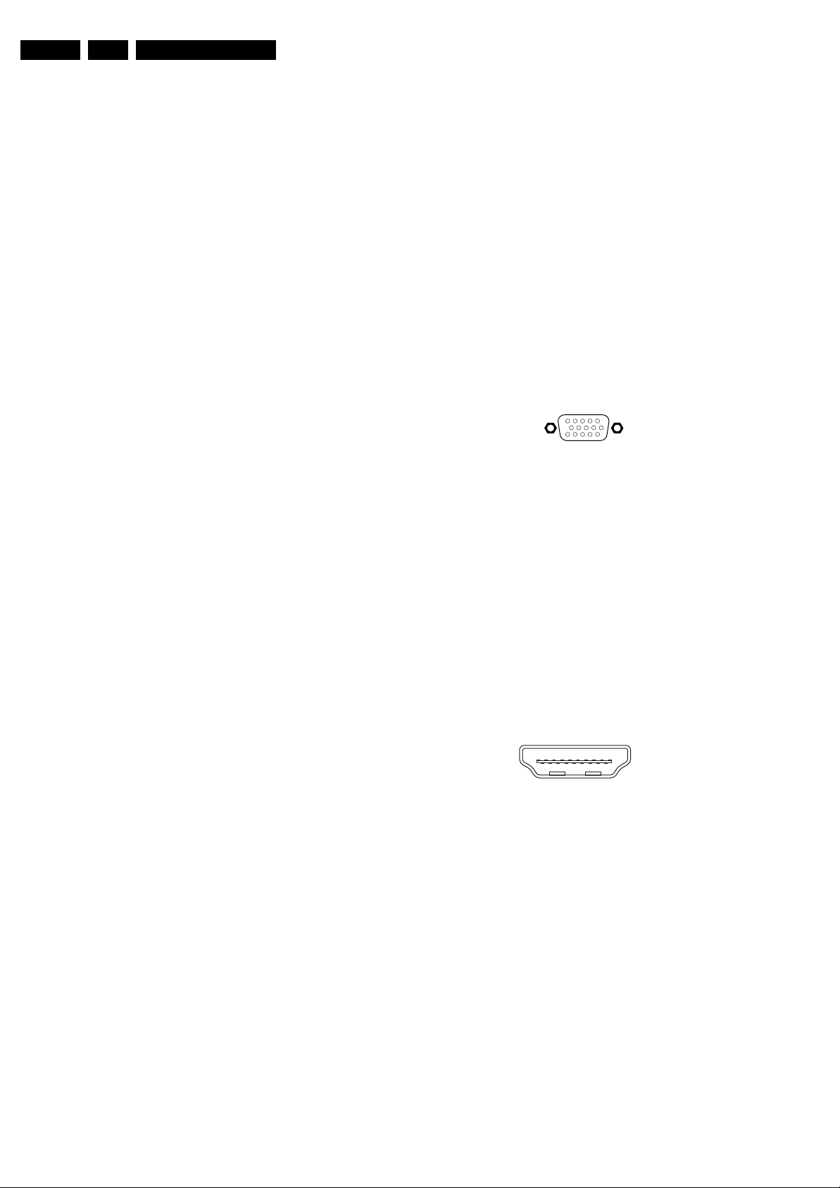
VGA: Video RGB - In
1
5
10
6
15
11
E_06532_002.eps
050404
Figure 1-1 VGA Connector
1 - Video Red 0.7 V
2 - Video Green 0.7 V
3 - Video Blue 0.7 V
4-n.c.
5 - Ground Gnd H
6 - Ground Red Gnd H
7 - Ground Green Gnd H
8 - Ground Blue Gnd H
9-+5V
+5 V j
DC
10 - Ground Sync Gnd H
11 - n.c.
12 - DDC_SDA DDC data j
13 - H-sync 0 - 5 V j
14 - V-sync 0 - 5 V j
15 - DDC_SCL DDC clock j
HDMI: Digital Video, Digital Audio - In
19
18 2
Figure 1-2 HDMI (type A) connector
1 - D2+ Data channel j
2 - Shield Gnd H
3 - D2- Data channel j
4 - D1+ Data channel j
5 - Shield Gnd H
6 - D1- Data channel j
7 - D0+ Data channel j
8 - Shield Gnd H
9 - D0- Data channel j
10 - CLK+ Data channel j
11 - Shield Gnd H
12 - CLK- Data channel j
13 - CEC
14 - n.c.
15 - DDC_SCL DDC clock j
16 - DDC_SDA DDC data jk
17 - Ground Gnd H
18 - +5V j
19 - HPD Hot Plug Detect j
20 - Ground Gnd H
/ 75 ohm j
PP
/ 75 ohm j
PP
/ 75 ohm j
PP
1
E_06532_017.eps
250505
Page 3
Technical Specifications, Connections, and Chassis Overview
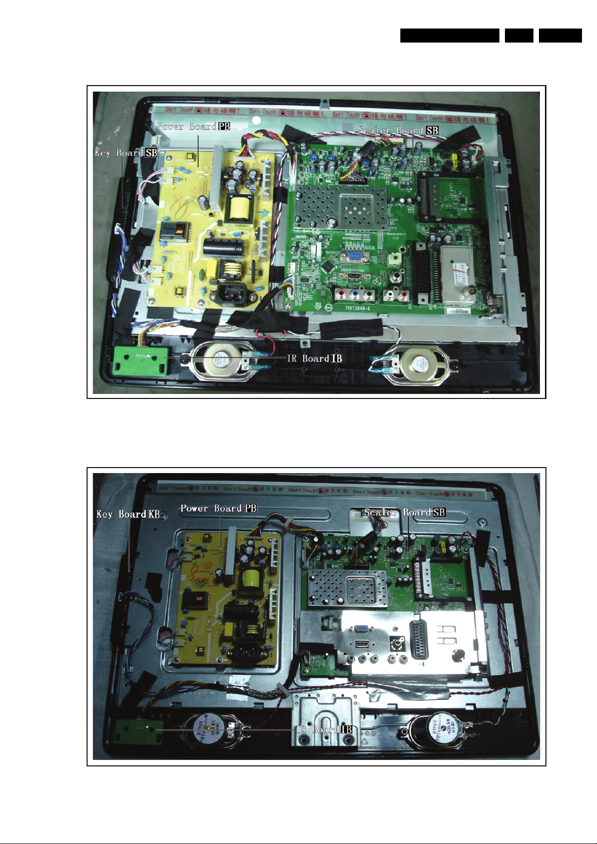
1.3 Chassis Overview
EN 3TPM1.3E LA 1.
Figure 1-3 Chassis Overview (19PFL3403D/10)
I_17570_007.eps
170408
Figure 1-4 Chassis Overview (22PFL3403D/10)
I_17570_008.eps
170408
Page 4

EN 4 TPM1.3E LA2.
Safety Instructions, Warnings, and Notes
2. Safety Instructions, Warnings, and Notes
Index of this chapter:
2.1 Safety Instructions
2.2 Warnings
2.3 Notes
2.1 Safety Instructions
Safety regulations require the following during a repair:
• Connect the set to the Mains/AC Power via an isolation
transformer (> 800 VA).
• Replace safety components, indicated by the symbol h,
only by components identical to the original ones. Any
other component substitution (other than original type) may
increase risk of fire or electrical shock hazard.
Safety regulations require that after a repair, the set must be
returned in its original condition. Pay in particular attention to
the following points:
• Route the wire trees correctly and fix them with the
mounted cable clamps.
• Check the insulation of the Mains/AC Power lead for
external damage.
• Check the strain relief of the Mains/AC Power cord for
proper function.
• Check the electrical DC resistance between the Mains/AC
Power plug and the secondary side (only for sets that have
a Mains/AC Power isolated power supply):
1. Unplug the Mains/AC Power cord and connect a wire
between the two pins of the Mains/AC Power plug.
2. Set the Mains/AC Power switch to the "on" position
(keep the Mains/AC Power cord unplugged!).
3. Measure the resistance value between the pins of the
Mains/AC Power plug and the metal shielding of the
tuner or the aerial connection on the set. The reading
should be between 4.5 Mohm and 12 Mohm.
4. Switch "off" the set, and remove the wire between the
two pins of the Mains/AC Power plug.
• Check the cabinet for defects, to prevent touching of any
inner parts by the customer.
2.2 Warnings
• All ICs and many other semiconductors are susceptible to
electrostatic discharges (ESD w). Careless handling
during repair can reduce life drastically. Make sure that,
during repair, you are connected with the same potential as
the mass of the set by a wristband with resistance. Keep
components and tools also at this same potential. Available
ESD protection equipment:
– Complete kit ESD3 (small tablemat, wristband,
connection box, extension cable and earth cable) 4822
310 10671.
– Wristband tester 4822 344 13999.
• Be careful during measurements in the high voltage
section.
• Never replace modules or other components while the unit
is switched "on".
• When you align the set, use plastic rather than metal tools.
This will prevent any short circuits and the danger of a
circuit becoming unstable.
2.3 Notes
2.3.1 General
• Measure the voltages and waveforms with regard to the
chassis (= tuner) ground (H), or hot ground (I), depending
on the tested area of circuitry. The voltages and waveforms
shown in the diagrams are indicative. Measure them in the
Service Default Mode (see chapter 5) with a colour bar
signal and stereo sound (L: 3 kHz, R: 1 kHz unless stated
otherwise) and picture carrier at 475.25 MHz for PAL, or
61.25 MHz for NTSC (channel 3).
• Where necessary, measure the waveforms and voltages
with (D) and without (E) aerial signal. Measure the
voltages in the power supply section both in normal
operation (G) and in stand-by (F). These values are
indicated by means of the appropriate symbols.
2.3.2 Schematic Notes
• All resistor values are in ohms, and the value multiplier is
often used to indicate the decimal point location (e.g. 2K2
indicates 2.2 kohm).
• Resistor values with no multiplier may be indicated with
either an "E" or an "R" (e.g. 220E or 220R indicates 220
ohm).
• All capacitor values are given in micro-farads (μ= x10
nano-farads (n= x10
• Capacitor values may also use the value multiplier as the
decimal point indication (e.g. 2p2 indicates 2.2 pF).
• An "asterisk" (*) indicates component usage varies. Refer
to the diversity tables for the correct values.
• The correct component values are listed in the Spare Parts
List. Therefore, always check this list when there is any
doubt.
2.3.3 BGA (Ball Grid Array) ICs
Introduction
For more information on how to handle BGA devices, visit this
URL: www.atyourservice.ce.philips.com (needs subscription,
not available for all regions). After login, select “Magazine”,
then go to “Repair downloads”. Here you will find Information
on how to deal with BGA-ICs.
BGA Temperature Profiles
For BGA-ICs, you must use the correct temperature-profile,
which is coupled to the 12NC. For an overview of these profiles,
visit the website www.atyourservice.ce.philips.com (needs
subscription, but is not available for all regions)
You will find this and more technical information within the
"Magazine", chapter "Repair downloads".
For additional questions please contact your local repair help
desk.
2.3.4 Lead-free Soldering
Due to lead-free technology some rules have to be respected
by the workshop during a repair:
• Use only lead-free soldering tin Philips SAC305 with order
code 0622 149 00106. If lead-free solder paste is required,
please contact the manufacturer of your soldering
equipment. In general, use of solder paste within
workshops should be avoided because paste is not easy to
store and to handle.
• Use only adequate solder tools applicable for lead-free
soldering tin. The solder tool must be able:
– To reach a solder-tip temperature of at least 400°C.
– To stabilize the adjusted temperature at the solder-tip.
– To exchange solder-tips for different applications.
• Adjust your solder tool so that a temperature of around
360°C - 380°C is reached and stabilized at the solder joint.
Heating time of the solder-joint should not exceed ~ 4 sec.
Avoid temperatures above 400°C, otherwise wear-out of
tips will increase drastically and flux-fluid will be destroyed.
To avoid wear-out of tips, switch “off” unused equipment or
reduce heat.
-9
), or pico-farads (p= x10
-12
-6
),
).
Page 5

Directions for Use
EN 5TPM1.3E LA 3.
• Mix of lead-free soldering tin/parts with leaded soldering
tin/parts is possible but PHILIPS recommends strongly to
avoid mixed regimes. If this cannot be avoided, carefully
clear the solder-joint from old tin and re-solder with new tin.
2.3.5 Alternative BOM identification
The third digit in the serial number (example:
AG2B0335000001) indicates the number of the alternative
B.O.M. (Bill Of Materials) that has been used for producing the
specific TV set. In general, it is possible that the same TV
model on the market is produced with e.g. two different types
of displays, coming from two different suppliers. This will then
result in sets which have the same CTN (Commercial Type
Number; e.g. 28PW9515/12) but which have a different B.O.M.
number.
By looking at the third digit of the serial number, one can
identify which B.O.M. is used for the TV set he is working with.
If the third digit of the serial number contains the number “1”
(example: AG1B033500001), then the TV set has been
manufactured according to B.O.M. number 1. If the third digit is
a “2” (example: AG2B0335000001), then the set has been
produced according to B.O.M. no. 2. This is important for
ordering the correct spare parts!
For the third digit, the numbers 1...9 and the characters A...Z
can be used, so in total: 9 plus 26= 35 different B.O.M.s can be
indicated by the third digit of the serial number.
Identification: The bottom line of a type plate gives a 14-digit
serial number. Digits 1 and 2 refer to the production centre (e.g.
AG is Bruges), digit 3 refers to the B.O.M. code, digit 4 refers
to the Service version change code, digits 5 and 6 refer to the
production year, and digits 7 and 8 refer to production week (in
example below it is 2006 week 17). The 6 last digits contain the
serial number.
MODEL :
PROD.NO:
32PF9968/10
AG 1A0617 000001
MADE IN BELGIUM
220-240V 50/60Hz
~
VHF+S+H+UHF
S
128W
BJ3.0E LA
E_06532_024.eps
260308
Figure 2-1 Serial number (example)
2.3.6 Board Level Repair (BLR) or Component Level Repair
(CLR)
If a board is defective, consult your repair procedure to decide
if the board has to be exchanged or if it should be repaired on
component level.
If your repair procedure says the board should be exchanged
completely, do not solder on the defective board. Otherwise, it
cannot be returned to the O.E.M. supplier for back charging!
2.3.7 Practical Service Precautions
• It makes sense to avoid exposure to electrical shock.
While some sources are expected to have a possible
dangerous impact, others of quite high potential are of
limited current and are sometimes held in less regard.
• Always respect voltages. While some may not be
dangerous in themselves, they can cause unexpected
reactions that are best avoided. Before reaching into a
powered TV set, it is best to test the high voltage insulation.
It is easy to do, and is a good service precaution.
3. Directions for Use
You can download this information from the following websites:
http://www.philips.com/support
http://www.p4c.philips.com
Page 6
EN 6 TPM1.3E LA4.
Mechanical Instructions
4. Mechanical Instructions
Index of this chapter:
1. Cable Dressing
2. Service Positions
3. Assy/Panel Removal
4. Re-assembly
4.1 Cable Dressing
Notes:
• Figures below can deviate slightly from the actual situation,
due to the different set executions.
• Follow the disassembly instructions in the described order.
Figure 4-1 Cable dressing (19PFL3403D/10)
I_17570_009.eps
170408
Page 7
Mechanical Instructions
EN 7TPM1.3E LA 4.
Figure 4-2 Cable dressing (22PFL3403D/10)
I_17570_010.eps
170408
Page 8
EN 8 TPM1.3E LA4.
Mechanical Instructions
4.2 Service Positions
For easy servicing of this set, there are a few possibilities
created:
• The buffers from the packaging (see figure “Rear cover”).
• Foam bars (created for Service).
4.2.1 Foam Bars
1
Required for sets
1
42"
E_06532_018.eps
171106
Figure 4-3 Foam bars
4.3 Assy/Panel Removal
4.3.1 Stand/Base
Remove the screws marked in red to remove the stand or base.
Figure 4-4 Remove Base (19PFL3403D)
I_17570_011.eps
180408
The foam bars (order code 3122 785 90580 for two pieces) can
be used for all types and sizes of Flat TVs. See figure “Foam
bars” for details. Sets with a display of 42” and larger, require
four foam bars [1]. Ensure that the foam bars are always
supporting the cabinet and never only the display.
Caution: Failure to follow these guidelines can seriously
damage the display!
By laying the TV face down on the (ESD protective) foam bars,
a stable situation is created to perform measurements and
alignments. By placing a mirror under the TV, you can monitor
the screen.
Figure 4-5 Remove Stand (22PFL3403D)
I_17570_012.eps
180408
Page 9
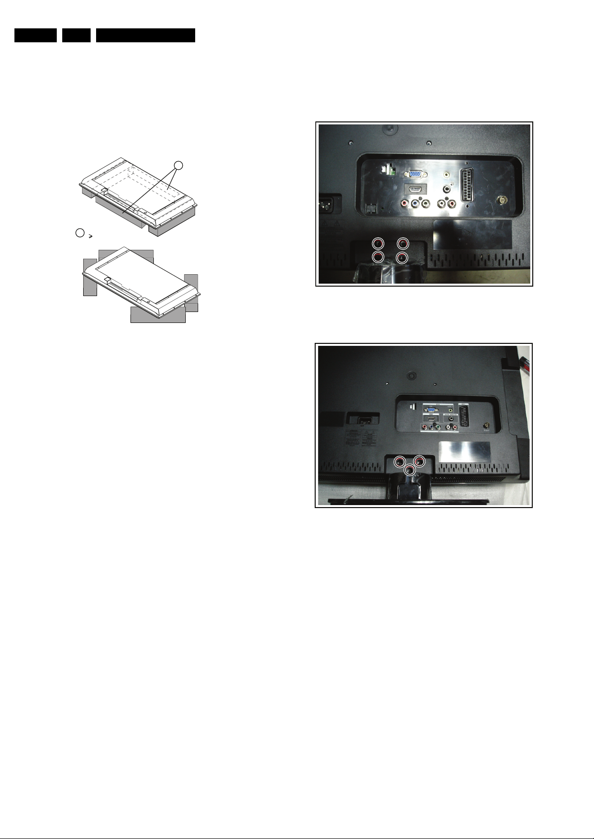
4.3.2 Rear Cover
1. Remove the screws marked in red, which secure the rear
cover.
2. Lift the rear cover from the cabinet. Make sure that wires
and flat foils are not damaged during cover removal.
Figure 4-6 Remove rear cover (19PFL3403D)
Mechanical Instructions
I_17570_013.eps
180408
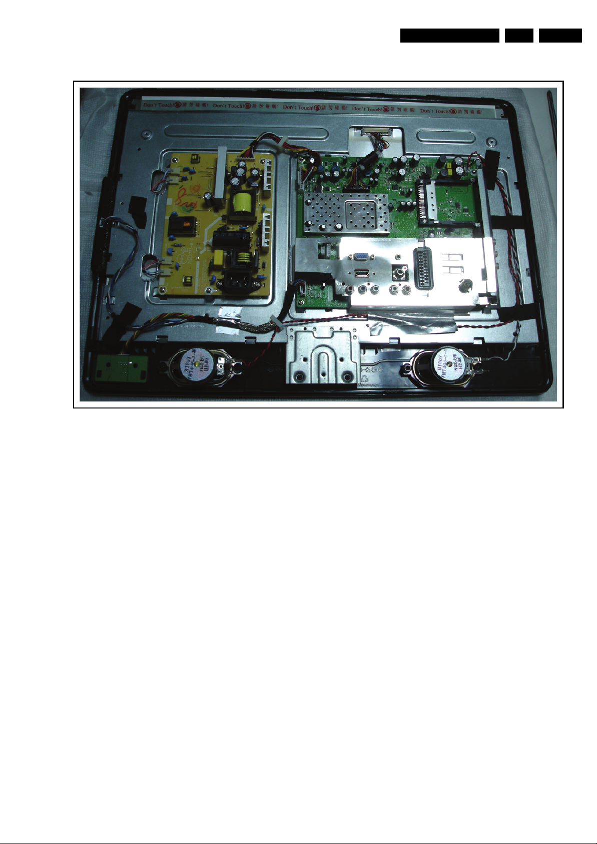
4.3.4 Shielding EMI
Figure 4-8 Power Board
EN 9TPM1.3E LA 4.
I_17570_015.eps
180408
Figure 4-7 Remove rear cover (22PFL3403D)
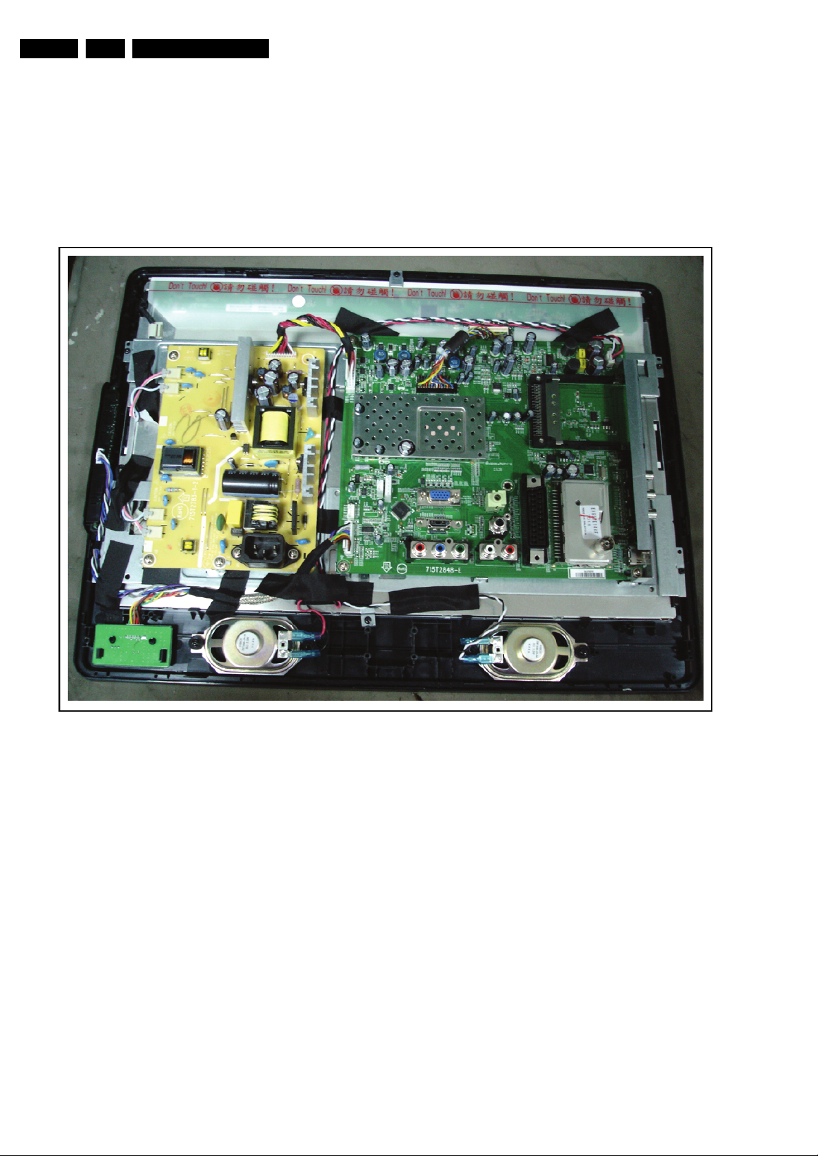
4.3.3 Power Board
1. Refer to next figure.
2. Unplug connectors marked in blue.
3. Release screws marked in red and remove the power
board.
When defective, replace the whole unit.
I_17570_014.eps
180408
1. Refer to next figure.
2. Release the screws marked in red and remove the
shielding-EMI.
When defective, replace the whole unit.
I_17570_016.eps
Figure 4-9 Shielding-EMI
180408
Page 10
EN 10 TPM1.3E LA4.
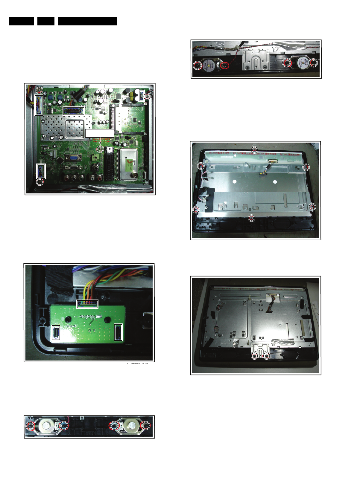
4.3.5 Scaler Board
1. Refer to next figure.
2. Unplug connectors marked in blue.
3. Release screws marked in red and remove the scaler
board.
When defective, replace the whole unit.
Mechanical Instructions
4.3.8 Bezel
Figure 4-13 Speakers (22PFL3403D/10)
I_17570_020.eps
180408
Figure 4-10 Scaler Board
4.3.6 IR Board
1. Refer to next figure
2. Unplug the connector marked in blue.
When defective, replace the whole unit.
22PFL3403D
ONLY
I_17570_017.eps
180408
1. Refer to next figures.
2. Remove the screws marked in red.
Figure 4-14 Bezel (19PFL3403D/10)
I_17570_021.eps
180408
Figure 4-11 IR Board
4.3.7 Speakers
1. Refer to next figure.
2. Remove the screws marked in red.
Figure 4-12 Speakers (19PFL3403D/10)
I_17570_019.eps
180408
Figure 4-15 Bezel (22PFL3403D/10)
I_17570_022.eps
180408
Page 11
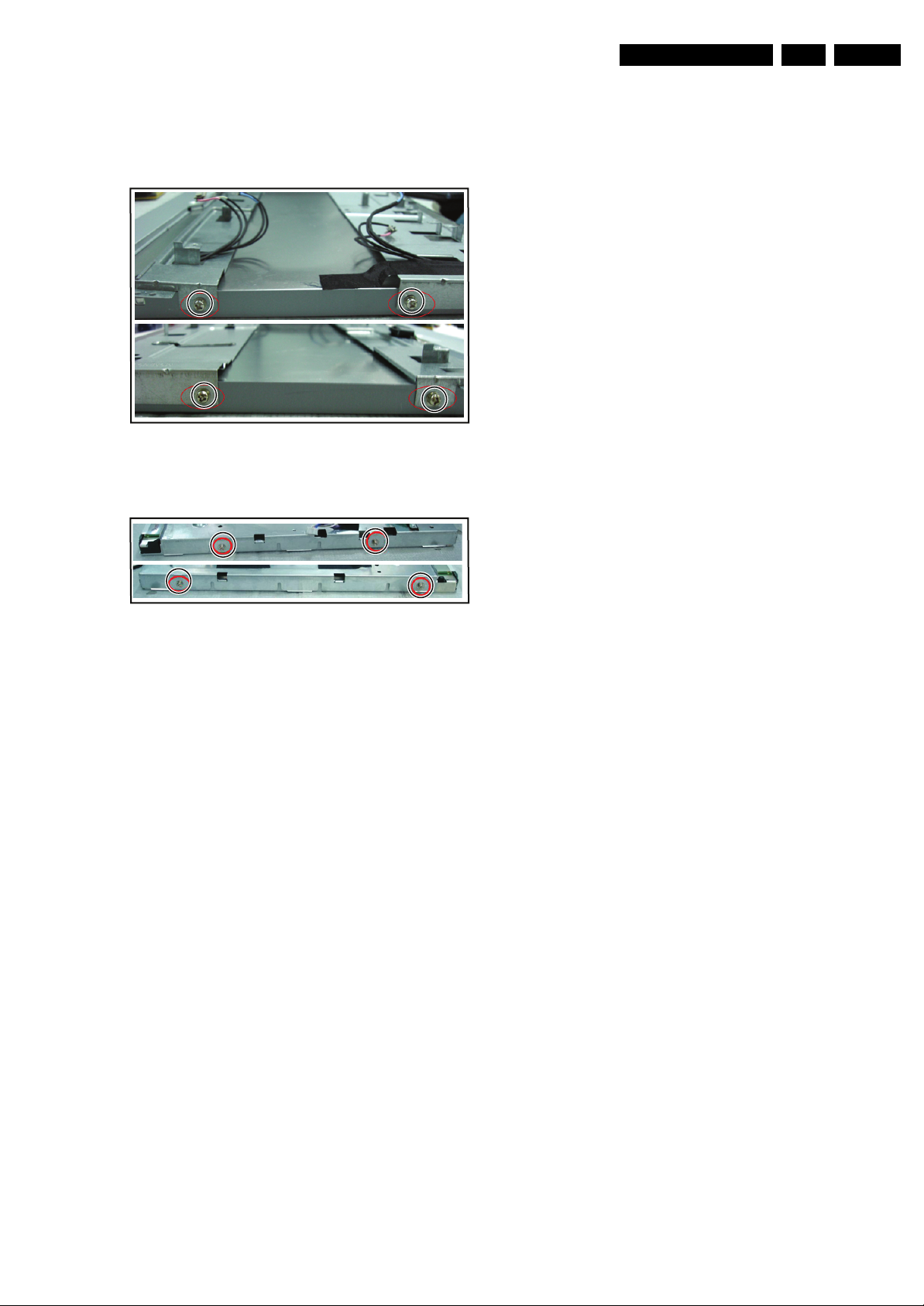
4.3.9 Bracket/Main Frame
1. Refer to next two figures.
2. Remove the screws marked in red.
Figure 4-16 Bracket (19PFL3403D/10)
Mechanical Instructions
I_17570_023.eps
180408
EN 11TPM1.3E LA 4.
Figure 4-17 Main Frame (22PFL3403D/10)
4.4 Set Re-assembly
To re-assemble the whole set, execute all processes in reverse
order.
Notes:
• While re-assembling, make sure that all cables are placed
and connected in their original position. See figure “Cable
dressing”.
I_17570_024.eps
180408
Page 12
EN 12 TPM1.3E LA5.
Service Modes, Error Codes, and Fault Finding
5. Service Modes, Error Codes, and Fault Finding
Index of this chapter:
5.1 Test Points
5.2 Service Mode
5.3 Service Tools
5.1 Test Points
This chassis is not equipped with test points in the service
printing. These test points are not specifically mentioned in the
service manual
5.2 Service Mode
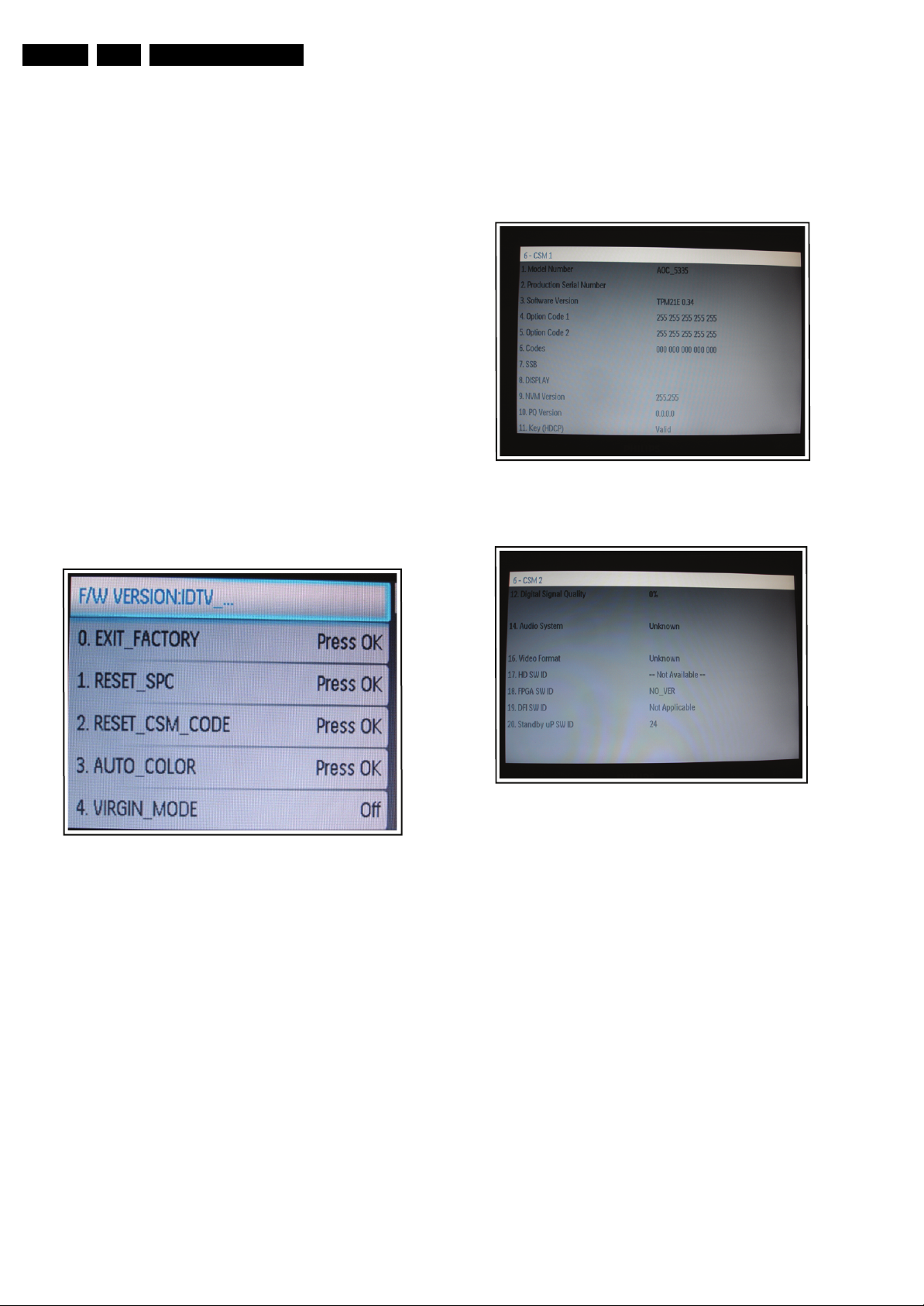
5.2.1 Factory Mode
How to Enter
To enter the Factory mode, please use the following method:
• Press the remote control codes ”062596”, and press “Info”.
key; Then you can press the “menu” key, select the
“factory” and press “OK” in order to carry out the factory
OSD.
Caution: This functions are viable for development and
service personal only, not for end customers
After entering factory mode, the following screen is visible, you
can select one of them to press OK according to the requested.
How to Navigate
By mean of the “CURSOR-DOWN/UP” knob on the RCtransmitter on the screen.
Contents of CSM
I_17570_027.eps
180408
Figure 5-2 CSM Menu1
Figure 5-1 Factory mode menu
How to EXIT
Choose ‘EXIT_FACTORY”, then press “OK” bottom on remote
control.
5.2.2 Customer Service Mode (CSM)
Purpose
When a customer is having problems with his TV-set, he can
call his dealer or the Customer Helpdesk.The service
technician can then ask the customer to activate the CSM in
order to identify the status of the set.Now, the service
technician can judge the severity of the complain.In many
cases, he can advise the customer how to solve the problem,
or he can decide if it is necessary to visit the customer. The
CSM is read only mode; therefore, modifications in this mode
are not possible.
How to Activate CSM
Key in the codes ”123654” via the standard RC transmitter to
enter the Customer Service Mode.
I_17570_025.eps
180408
I_17570_028.eps
Figure 5-3 CSM Menu2
Menu Explanation
1. Model Number: AOC_5335
2. Production Serial Number: Product serial no.
3. Software Version
4. Option Code 1: Error buffer contents.
5. Option Code 2: Error buffer contents.
6. Codes
7. SSB
8. DISPLAY
9. NVM Version: The version of EEPROM.
10. PQ Version: The version of Picture Quality.
11. Key (HDCP): Indicates if the keys are valid.
12. Digital Signal Quality
13. None
14. Audio System
15. None
16. Video Format
17. HD SW ID: The version of the hardware.
18. FPGA SW ID
19. DFI SW ID
20. Stand-by uP SW ID: The version of the MCU.
How to exit
Press ”MENU” on the RC-transmitter.
180408
Page 13
Service Modes, Error Codes, and Fault Finding
5.3 Service Tools
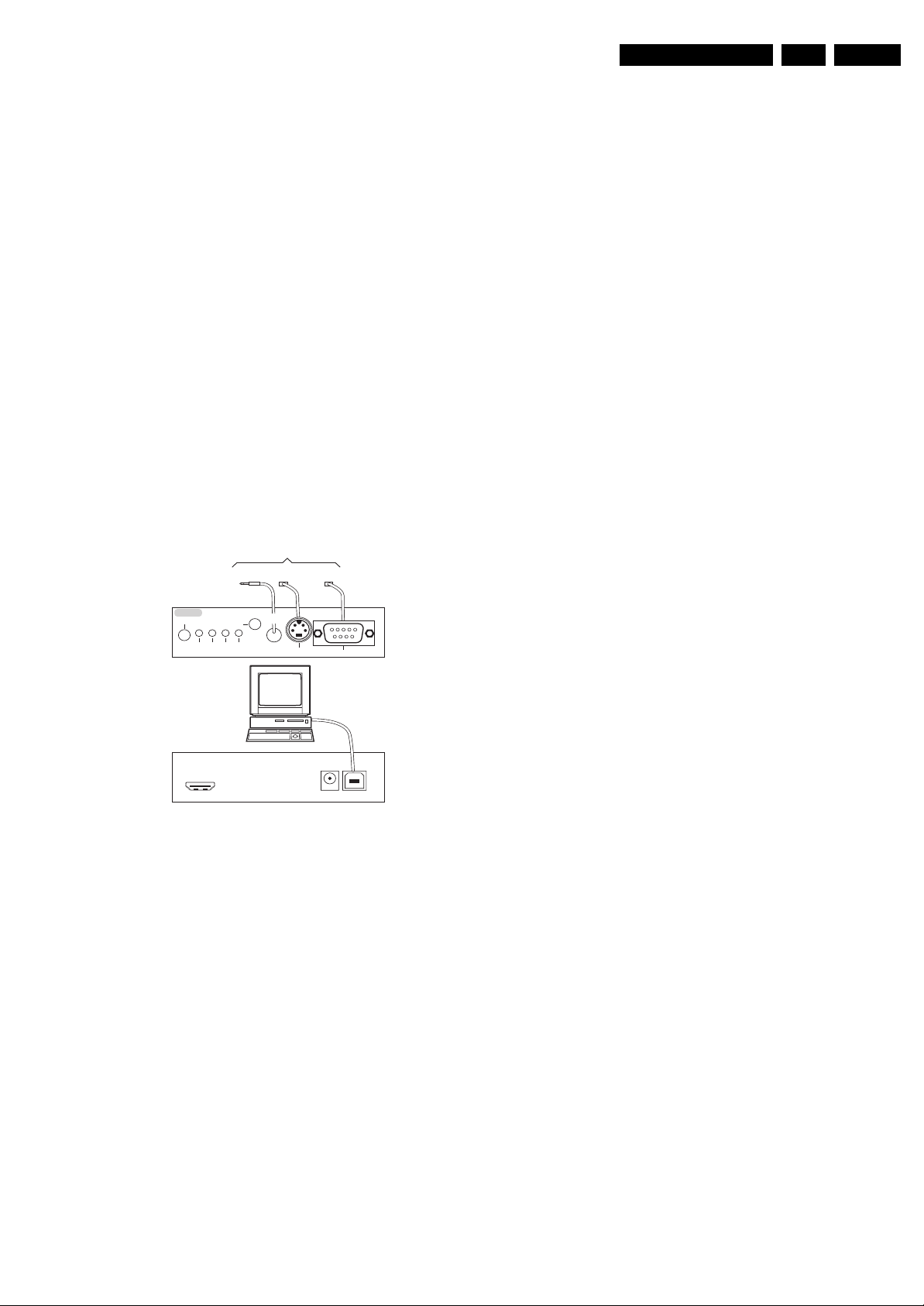
5.3.1 ComPair
Introduction
ComPair (Computer Aided Repair) is a Service tool for Philips
Consumer Electronics products. and offers the following:
1. ComPair helps you to quickly get an understanding on how
to repair the chassis in a short and effective way.
2. ComPair allows very detailed diagnostics and is therefore
capable of accurately indicating problem areas. You do not
have to know anything about I
yourself, because ComPair takes care of this.
3. ComPair speeds up the repair time since it can
automatically communicate with the chassis (when the uP
is working) and all repair information is directly available.
4. ComPair features TV software upgrade possibilities.
Specifications
ComPair consists of a Windows based fault finding program
and an interface box between PC and the (defective) product.
The (new) ComPair II interface box is connected to the PC via
an USB cable. For the TV chassis, the ComPair interface box
and the TV communicate via a bi-directional cable via the
service connector(s).
2
C or UART commands
EN 13TPM1.3E LA 5.
How to Connect
This is described in the ComPair chassis fault finding database.
TO TV
TO
UART SERVICE
I2C SERVICE
CONNECTOR
CONNECTOR
2
I
C
PC
ComPair II Developed by Philips Brugge
Optional power
5V DC
TO
RS232 /UART
E_06532_036.eps
150208
ComPair II
RC in
Optional
Switch
Power ModeLink/
Activity
HDMI
I
2
C only
UART SERVICE
RC out
TO
CONNECTOR
Multi
function
Figure 5-4 ComPair II interface connection
Caution: It is compulsory to connect the TV to the PC as
shown in the picture above (with the ComPair interface in
between), as the ComPair interface acts as a level shifter. If
one connects the TV directly to the PC (via UART), ICs will be
blown!
How to Order
ComPair II order codes:
• ComPair II interface: 3122 785 91020.
• For SW see Philips service website.
•ComPair I
2
C interface cable: 9965 100 09269.
Note: If you encounter any problems, contact your local
support desk.
Page 14

EN 14 TPM1.3E LA5.
Personal Notes:
Service Modes, Error Codes, and Fault Finding
E_06532_012.eps
131004
Page 15
Block Diagrams, Test Point Overview, and Waveforms
6. Block Diagrams, Test Point Overview, and Waveforms
Wiring Diagram 19PFL3403D/10
WIRING DIAGRAM 19”
15TPM1.3E LA 6.
Key
Board
5 Pin
CN101
Panel
5
1
095T8018 3DH06 LVDS Cable
11
11 Pin
CN902
CN802
CN801
Power Board
1
095T 82011X511
WIRE HARNESS
12
CN902
12 Pin
1
1
MT5335PGU
U401
Scaler IC
30 Pin
CN301
Main Board
30
CN602
Head Phone
4 Pin
4
1
WIRE HARNESS
095T8014 4X551
CN804
CN803
IR Board
AC IN
CN901
1
6 Pin
CN1
VIDEO
AUDIO R/L
11
095T801411X510
WIRE HARNESS
11Pin
CN404
S-VIDEO
HDMI
1
6
Speaker R/L
I_17780_031.eps
170408
Page 16
Block Diagrams, Test Point Overview, and Waveforms
Wiring Diagram 22PFL3403D/10
WIRING DIAGRAM 22”
16TPM1.3E LA 6.
Key
Board
5 Pin
CN101
Panel
5
1
095T8018 3XH06 LVDS Cable
11
11 Pin
CN902
CN802
CN801
Power Board
1
095T 82011X503
WIRE HARNESS
12
CN902
12 Pin
1
1
MT5335PGU
U401
Scaler IC
30 Pin
CN301
Main Board
30
CN602
Head Phone
4 Pin
4
1
WIRE HARNESS
095T8014 4D553
CN804
CN803
IR Board
AC IN
CN901
1
6 Pin
CN1
VIDEO
AUDIO R/L
11
095T801411D509
WIRE HARNESS
11Pin
CN404
S-VIDEO
HDMI
1
6
Speaker R/L
I_17780_031.eps
170408
Page 17
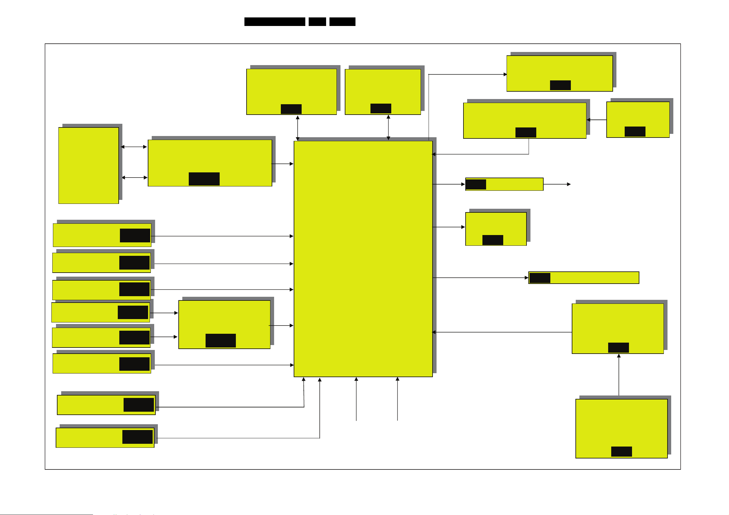
Block Diagrams, Test Point Overview, and Waveforms
Block Diagram Scaler Board
Power
Board
16V
Power
3.3V,2.5V,1.8V,1.2V,1.1V
DDR SDRAM
HY5DU121622DTP-D43
2.5V
SB-09
MT5335PGU
17TPM1.3E LA 6.
Sub MCU
WT6702F_OG200WT
3.3V
SB-11
Audio AMP
TDA8932BTW
12V
SB-15
Common Interface Controller
MT8295
3.3V,1.8V
SB-18
PCMCIA
5V,3.3V
SB-18
D-SUB/PC-VGA
SCART
S-Video
HDMI 1
HDMI 2
5V
SB-01
SB-04
SB-05
SB-13
SB-13
SB-19
HDMI MUX
TMDS251PAGR
5V,3.3V
SB-13
MPEG-1 layer I/II decoding
Audio ADC
Audio DAC
3D surround processing with
Virtual surround
Automatic volume control
Audio I/F
2-D Graphic
De-interlace
VADCx4
HDMI In I/F
Digital TV Demodulator
Analog TV IF Demodulator
TV audio demodulator
3.3V,2.5V,1.2V,1.1V
SB-14
SPIDF OUT
2.5V
SB-18
EARPHONE AMP
SB-10
Headphone
Flash MX25L3205DMI-12G
Channel demodulator
MT5133
3.3V
SB-17
YPbPr/L/R
Audio R/L of CVBS
Audio R/L of PC
SB-02
SB-03
SB-01
IR
Keypad
TUNER
ENG37E14KF
5V
SB-17
I_17780_030.eps
170408
Page 18
Circuit Diagrams and PWB Layouts
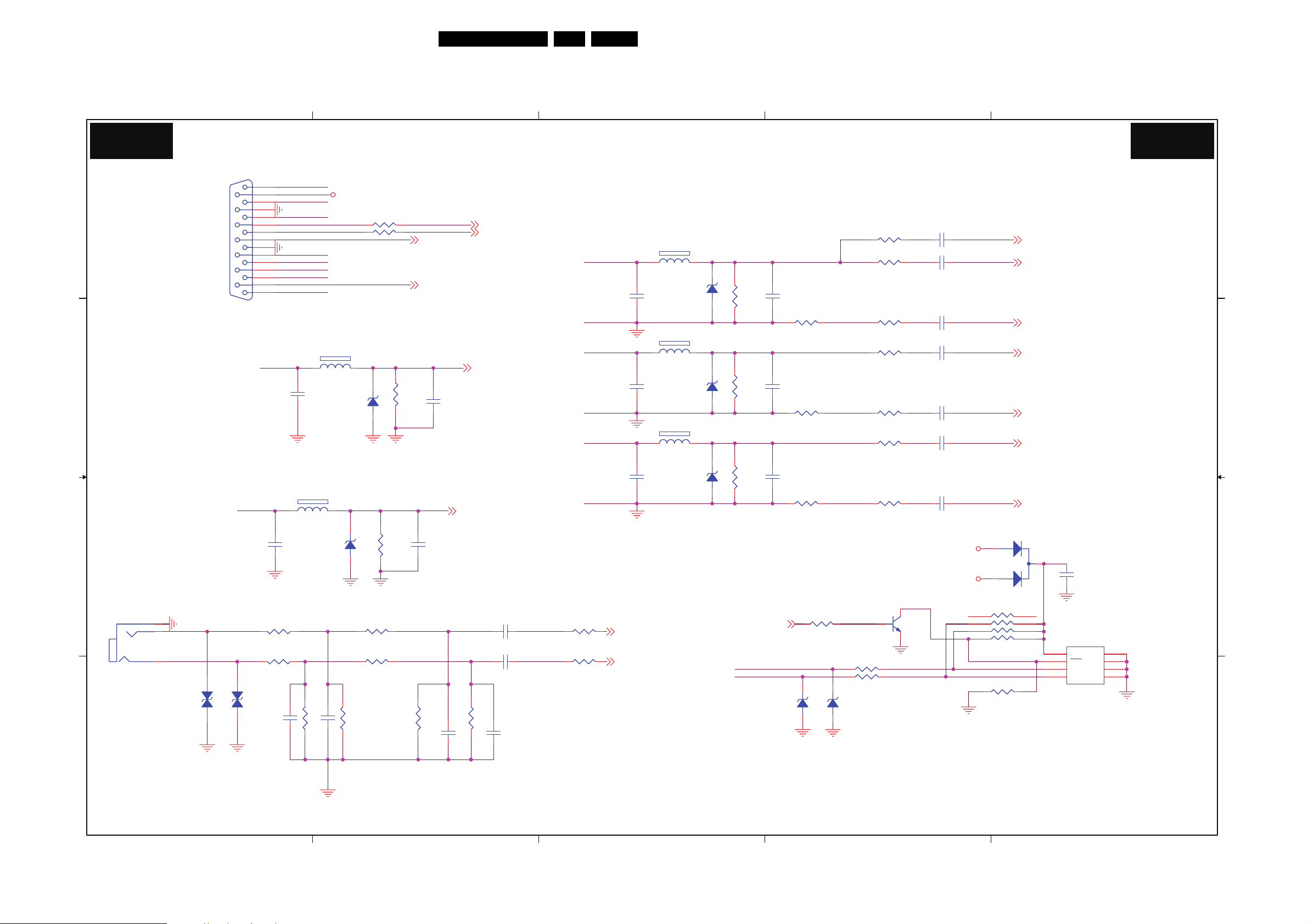
7. Circuit Diagrams and PWB Layouts
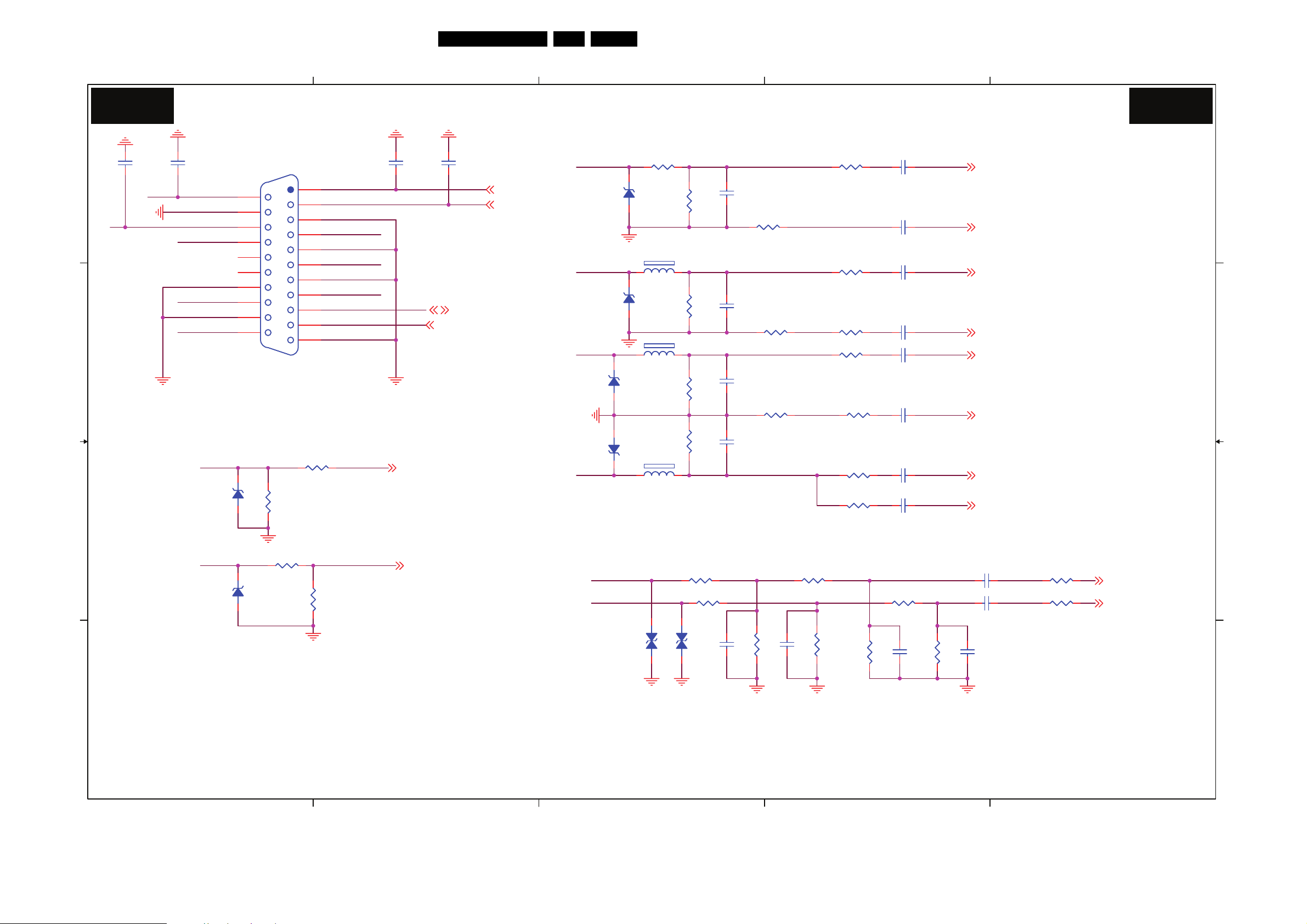
Scaler (19"): VGA IN/L/R
5
18TPM1.3E LA 7.
4
3
2
1
SB01
D
C C
B B
CN109
CN109
PHONEJACK
PHONEJACK
VGA IN/L/R
CN108
CN108
DB15
DB15
1
VGAL_IN
2
VGAR_IN
3
ZD130
ZD130
1
9
2
10
3
11
4
12
5
13
6
14
7
15
8
HSYNC#
VSYNC#
R218
R218
1K OHM 1/10W
1K OHM 1/10W
R219
R219
1K OHM 1/10W
1K OHM 1/10W
ZD131
ZD131
RED
GRN
BLU
HSYNC#
RED_GND
VSYNC#
GRN_GND
BLU_GND
L113
L113
1 2
80 OHM
80 OHM
C192
C192
5pF
5pF
L114
L114
1 2
80 OHM
80 OHM
ZD127
ZD127
C196
C196
UDZSNP5.6B
UDZSNP5.6B
5pF
5pF
VGA_PLUGPWR
R244 NCR244 NC
R245 NCR245 NC
VGASDA_IN
VGASCL_IN
ZD125
ZD125
UDZSNP5.6B
UDZSNP5.6B
1 2
R220
R220
3K OHM 1/10W
3K OHM 1/10W
R221
R221
3K OHM 1/10W
3K OHM 1/10W
2.2K OHM 1/10W
2.2K OHM 1/10W
1 2
R203
R203
2.2K OHM 1/10W
2.2K OHM 1/10W
R198
R198
VGASDA_IN
VGASCL_IN
C107
C107
NC/5pF
NC/5pF
C109
C109
NC/5pF
NC/5pF
U0RX 12
U0TX 12
HSYNC 4,13
VSYNC 4,13
C120 10uF/10VC120 10uF/10V
C122 10uF/10VC122 10uF/10V
R204
R204
20K OHM 1/10W
20K OHM 1/10W
R206
R206
20K OHM 1/10W
20K OHM 1/10W
GRN
GRN_GND
BLU
BLU_GND
RED
RED_GND
AIN0_L 10
AIN0_R 10
L111
L111
1
80 OHM
80 OHM
C187
C187
UDZSNP5.6B
UDZSNP5.6B
5pF
5pF
L112
L112
1 2
80 OHM
80 OHM
C190
C190
UDZSNP5.6B
UDZSNP5.6B
5pF
5pF
L101
L101
1 2
80 OHM
80 OHM
UDZSNP5.6B
UDZSNP5.6B
C194
C194
5pF
5pF
ZD121
ZD121
ZD124
ZD124
ZD126
ZD126
SB01
R188
0 OHM 1/10W
0 OHM 1/10W
R189
2
C102
1 2
1 2
1 2
R191
R191
R195
R195
R200
R200
HDMIED_WP14,20
VGASCL_IN
VGASDA_IN
C102
NC/5pF
NC/5pF
R192
R192
0 OHM 1/10W
75 OHM +-1% 1/8W
75 OHM +-1% 1/8W
75 OHM +-1% 1/8W
75 OHM +-1% 1/8W
75 OHM +-1% 1/8W
75 OHM +-1% 1/8W
0 OHM 1/10W
C106
C106
NC/5pF
NC/5pF
R196
R196
0 OHM 1/10W
0 OHM 1/10W
C103
C103
NC/5pF
NC/5pF
R201
R201
0 OHM 1/10W
0 OHM 1/10W
R248 10K OHM 1/10WR248 10K OHM 1/10W
ZD128
ZD128
R189
39 OHM +-1% 1/10W
39 OHM +-1% 1/10W
R193
R193
100 OHM 1/10W
100 OHM 1/10W
R194
R194
39 OHM +-1% 1/10W
39 OHM +-1% 1/10W
R197
R197
100 OHM 1/10W
100 OHM 1/10W
R199
R199
39 OHM +-1% 1/10W
39 OHM +-1% 1/10W
R202
R202
100 OHM 1/10W
100 OHM 1/10W
R205 100 OHM 1/10WR205 100 OHM 1/10W
R207 100 OHM 1/10WR207 100 OHM 1/10W
ZD129
ZD129
H : WP ENABLE
L : WP DISABLE
VGA_PLUGPWR
Q102
Q102
MMBT3904
MMBT3904
C101 4700pFC101 4700pF
C1860.01uF/25VC1860.01uF/25V
C188 0.01uF/25VC188 0.01uF/25V
C1890.01uF/25VC1890.01uF/25V
C191 0.01uF/25VC191 0.01uF/25V
C193 0.01uF/25VC193 0.01uF/25V
C195 0.01uF/25VC195 0.01uF/25V
+5VSB
RN101
RN101
4.7KOHM +-5% 1/16W
4.7KOHM +-5% 1/16W
SOG 4
GP 4
GN 4
BP 4
BN 4
RP 4
RN 4
D101 BAT54CD101 BAT54C
2
1
1
2
3
4
R165
R165
NC/0 OHM 1/10W
NC/0 OHM 1/10W
8
7
6
5
3
8
7
6
5
C197
C197
0.1UF16V
0.1UF16V
U105
U105
1
E0
VCC
WC
SCL
SDA
M24C02-WDW6P
M24C02-WDW6P
VSS
2
E1
3
E2
4
R188
NEARLY ICNEARLY VGA CON.
ZD124 C3 ZD121 D3
C122 B4 C192 C5
C103 C3 R223 A4
C196 B5 C195 B2
ZD130 A5 R204 B3
R200 C3 R202 B2
RN101 B2 R219 B5
R222 A5 CN109 B5
C106 C3 ZD131 A5
R192 C2 C194 C3
C191 C2 R194 C2
R218 B5 Q102 B2
R188 D2 R193 C2
C186 D2 C182 A4
C101 D2 R205 B2
ZD125 C4 D101 B2
R198 C4 ZD127 B4
R203 B4 C102 D3
L112 C3 C181 A5
R191 D3 L114 B5
R165 A2 ZD128 A2
R244 D4 R221 B4
C136 A4 L101 C3
R189 D2 R195 C3
C109 B4 R220 B4
9 C2 U105 B1
C18
C190 C3 R197 C2
ZD126 C3 R199 C2
C135 A4 R207 A2
C188 C2 R248 B2
R196 C2 ZD129 A2
R225 A4 R245 D4
R224 A4 L111 D3
C197 B1 C193 C2
C187 D3 C120 B4
L113 C4 R201 B2
CN108 D5 C107 C4
R206 B3
D
1 2
1 2
VPORT0603100KV05
VPORT0603100KV05
VPORT0603100KV05
VPORT0603100KV05
A A
5
C181 470pFC181 470pF
R222
R222
R223
R223
C182 470pFC182 470pF
100K OHM 1/10W
100K OHM 1/10W
100K OHM 1/10W
100K OHM 1/10W
R224
R224
4
30K OHM 1% 1/10W
30K OHM 1% 1/10W
R225
R225
30K OHM 1% 1/10W
30K OHM 1% 1/10W
C136 33pFC136 33pF
3
C135 33pFC135 33pF
1 2
UDZSNP5.6B
UDZSNP5.6B
1 2
UDZSNP5.6B
UDZSNP5.6B
I_17780_011.eps
2
1
170408
Page 19
Circuit Diagrams and PWB Layouts
Scaler (19"): YPbPr/L/R & SPDIF
5
19TPM1.3E LA 7.
4
3
2
1
SB02 SB02
CN105
CN105
D D
JACK
JACK
C C
CN106
CN106
JACK
JACK
B B
10
A A
2
1
4
3
6
5
2
1
4
3
ASPDIF
PR0_IN
PB_GND
PB0_IN
PB_GND
Y0_IN
Y_GND
ZD119
ZD119
1 2
VPORT0603100KV05
VPORT0603100KV05
100 OHM 1/10W
100 OHM 1/10W
C119
C119
100pF
100pF
100 OHM 1/10W
100 OHM 1/10W
1/8 River
R183
R183
Y0_IN
Y_GND
PB0_IN
PB_GND
PR0_IN
R175 1K OHM 1/10WR175 1K OHM 1/10W
R176 1K OHM 1/10WR176 1K OHM 1/10W
ZD120
ZD120
1 2
VPORT0603100KV05
VPORT0603100KV05
R185
R185
NEARLY YPBPR CONNECTOR
L108
L108
1 2
80 OHM
80 OHM
C171
C171
100pF
100pF
L109
L109
1 2
80 OHM
80 OHM
C172
C172
100pF
100pF
C173
C173
100pF
100pF
L110
L110
1 2
80 OHM
80 OHM
C198
C198
470pF
470pF
R184
R184
1 2
30 OHM
30 OHM
1/8 River
R186NCR186
NC
ZD116
ZD116
UDZSNP5.6B
UDZSNP5.6B
ZD117
ZD117
UDZSNP5.6B
UDZSNP5.6B
ZD118
ZD118
UDZSNP5.6B
UDZSNP5.6B
Change to 75 OHM 1/8W
R177
R177
100K OHM 1/10W
100K OHM 1/10W
1/8 River
Y0_IN_OUT
R209
R209
75 OHM +-1% 1/8W
75 OHM +-1% 1/8W
PB0_IN_OUT
R210
R210
75 OHM +-1% 1/8W
75 OHM +-1% 1/8W
R211
R211
75 OHM +-1% 1/8W
75 OHM +-1% 1/8W
PR0_IN_OUT
YPBPR0L_IN
YPBPR0R_IN
C199
C199
470pF
470pF
C183
C183
0.1UF16V
0.1UF16V
C185
C185
100pF
100pF
12
R105
R105
0 OHM 1/10W
0 OHM 1/10W
R106
R106
68 OHM 1/10W
68 OHM 1/10W
R107
R107
100 OHM 1/10W
100 OHM 1/10W
R108
R108
68 OHM 1/10W
68 OHM 1/10W
R110
R110
100 OHM 1/10W
100 OHM 1/10W
R111
R111
68 OHM 1/10W
68 OHM 1/10W
R129
R129
3K OHM 1/10W
3K OHM 1/10W
R130
R130
3K OHM 1/10W
3K OHM 1/10W
R178
R178
100K OHM 1/10W
100K OHM 1/10W
SPDIF_OUT
---><---|>
ZD101
ZD101
VPORT0603100KV05
VPORT0603100KV05
C104 4700pFC104 4700pF
C105 0.01uF/25VC105 0.01uF/25V
C108 0.01uF/25VC108 0.01uF/25V
C111 0.01uF/25VC111 0.01uF/25V
C114 0.01uF/25VC114 0.01uF/25V
C116 0.01uF/25VC116 0.01uF/25V
30K OHM 1/10W
30K OHM 1/10W
R243
R243
CN107
CN107
2
1
JACK
JACK
SOY1
Y1P
Y1N
PB1P
PBR1N
PR1P
NEARLY MT5335
C13110uF/10VC13110uF/10V
C13210uF/10VC13210uF/10V
C20833pFC20833pF
C209 33pFC209 33pF
30K OHM 1/10W
30K OHM 1/10W
R242
R242
R246
R246
20K OHM 1/10W
20K OHM 1/10W
R247
R247
20K OHM 1/10W
20K OHM 1/10W
SOY06
Y0P6
Y0N6
PB0P6
PBR0N6
PR0P6
SOY1
Y1P
Y1N
PB1P
PBR1N
PR1P
AIN1_L 10
AIN1_R 10
SOY0
Y0P
Y0N
PB0P
PBR0N
PR0P
AV1 2
AV1 2
AV1 2
TP101TP101
TP106TP106
107
108
109
114
115
116
118
119
120
121
122
123
112
111
FB101
FB101
BEAD
BEAD
FB107
FB107
BEAD
BEAD
FB108
FB108
BEAD
BEAD
U401E
U401E
SOY0
Y0P
Y0N
PB0P
PBR0N
PR0P
SOY1
Y1P
Y1N
PB1P
PBR1N
PR1P
TN1
TP1
MT5335PGU
MT5335PGU
DVDD12_VGA
AVSS12_RGBADC
AVDD12_RGBADC
AVSS12_RGBFE
AVDD12_RGBFE
RP
RN
BP
BN
GP
GN
VSYNC
HSYNC
SOG
DVDD12_VGA
C174
C174
1uF/16V
1uF/16V
AVDD12_RGBADC
C176
C176
10uF/10V
10uF/10V
AVSS12_RGBADC
AVDD12_RGBFE
C179
C179
1uF/16V
1uF/16V
AVSS12_RGBFE
117
113
110
105
101
104
106
98
99
102
103
96
97
100
C175
C175
0.1UF16V
0.1UF16V
C177
C177
0.1UF16V
0.1UF16V
C180
C180
0.1UF16V
0.1UF16V
DVDD12_VGA
AVSS12_RGBADC
AVDD12_RGBADC
AVSS12_RGBFE
AVDD12_RGBFE
RP 3
RN 3
BP 3
BN 3
GP 3
GN 3
VSYNC 3,13
HSYNC 3,13
SOG 3
CN107 B3 R176 B5
R242 B3 ZD118 C4
C199 B4 C175 C1
FB107 B2 R246 C3
R110 C4 R177 B4
C179 B2 C185 A4
C132 B3 R183 B5
C209 B3 CN106 C5
R211 C4 C114 C3
R175 C5 C119 A5
C116 C3 C172 D4
R243 B3 R186 A4
C131 C3 C180 B1
C208 B3 FB101 C2
C104 D3 R108 D4
ZD119 B5 C171 D4
R106 D3 R105 D3
C177 B1 ZD120 B5
C108 D3 R185 A5
L109 D4 C174 C2
R129 C3 C105 D3
ZD101 A4 L108 D4
C111 D3
R210 D4
R111 C4 ZD117 D4
R130 B3 R178 B4
C198 B4 R247 B3
U401 D2 ZD116 D4
C176 B2 C183 B4
FB108 B2 L110 C4
R184 B4 CN105 D5
R107 D4 C173 C4
R209 D4
NC DVD part
YPbPr/L/R & SPDIF
I_17780_012.eps
5
4
3
2
1
170408
Page 20
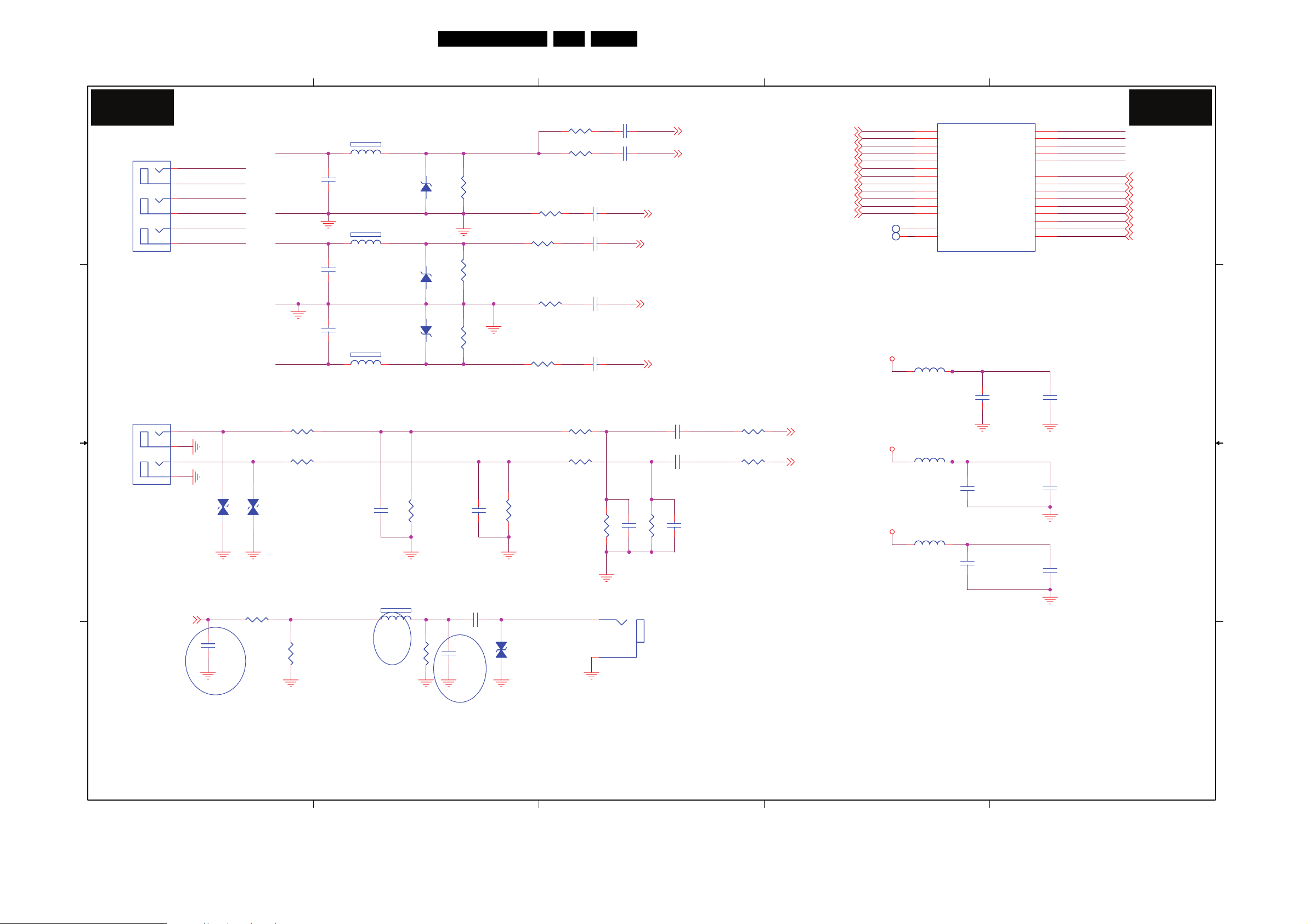
Circuit Diagrams and PWB Layouts
Scaler (19"): S-Video/CVBS/L/R
5
20TPM1.3E LA 7.
4
3
2
1
SB03 SB03
S-VIDEO/CVBS/L/R
U401F
CN103
CN103
SC1_IN
D
CN104
CN104
JACK
JACK
2
C
4
2
6
DIN JACK
DIN JACK
7
9
8
4
6
5
1
3
AV1 _IN
AV1L_IN
AV1 R_I N
3
1
5
SY1_IN
SY1_IN
SC1_IN
R162
R162
27 OHM 1/10W
27 OHM 1/10W
ZD111
ZD111
UDZSNP5.6B
UDZSNP5.6B
R166
R166
27 OHM 1/10W
27 OHM 1/10W
ZD112
ZD112
UDZSNP5.6B
UDZSNP5.6B
NEARLY AV CONNECTOR NEARLY MT5380
R163
R163
100 OHM 1/10W
100 OHM 1/10W
C152
R164
R164
47 OHM 1/10W
47 OHM 1/10W
R168
R168
47 OHM 1/10W
47 OHM 1/10W
C152
47pF
47pF
C156
C156
47pF
47pF
R167
R167
100 OHM 1/10W
100 OHM 1/10W
CVBS018
C151 0.047uFC151 0.047uF
C154 0.047uFC154 0.047uF
Near Connector
AV1R_IN
AV1 L_I N
B
A A
R226 1K OHM 1/10WR226 1K OHM 1/10W
R227 1K OHM 1/10WR227 1K OHM 1/10W
ZD113
ZD113
1 2
1 2
VPORT0603100KV05
VPORT0603100KV05
VPORT0603100KV05
VPORT0603100KV05
ZD114
ZD114
C200 470pFC200 470pF
R228
R228
100K OHM 1/10W
100K OHM 1/10W
R232
R232
3K OHM 1/10W
3K OHM 1/10W
C201 470pFC201 470pF
R229
R229
100K OHM 1/10W
100K OHM 1/10W
R233
R233
3K OHM 1/10W
3K OHM 1/10W
C202 33pFC202 33pF
30K OHM 1/10W
30K OHM 1/10W
R230
R230
AV1 _IN
R171
R171
27 OHM 1/10W
27 OHM 1/10W
ZD115
ZD115
UDZSNP5.6B
UDZSNP5.6B
C157 2.2uF/16VC157 2.2uF/16V
C160 2.2uF/16VC160 2.2uF/16V
30K OHM 1/10W
30K OHM 1/10W
R231
R231
C20333pFC20333pF
R173
R173
47 OHM 1/10W
47 OHM 1/10W
R169
R169
20K OHM 1/10W
20K OHM 1/10W
R170
R170
20K OHM 1/10W
20K OHM 1/10W
C167
C167
47pF
47pF
R174
R174
0 OHM 1/10W
0 OHM 1/10W
R172
R172
100 OHM 1/10W
100 OHM 1/10W
C164 0.047uFC164 0.047uF
C168 1uF/16VC168 1uF/16V
Close to MT5382p
R179
R179
100 OHM 1/10W
100 OHM 1/10W
R182NCR182
NC
SY1
SC1
AIN2_R 10
AIN2_L 10
CVBS1
GND_CVBS
C117
C117
0.047uF
0.047uF
CVBS1
SY06
SC06
SY1
SC1
D2SA
TP105TP105
AV2 5
AV2 5
C161
C161
4.7uF/10V
4.7uF/10V
AV2 5
AV2 5
132
130
129
128
127
126
125
136
FB103
FB103
BEAD
BEAD
FB104
FB104
BEAD
BEAD
FB105
FB105
BEAD
BEAD
FB106
FB106
BEAD
BEAD
U401F
CVBS0
CVBS1
CVBS2
SY0
SC0
SY1
SC1
D2SA
DVDD25_VADC
DVSS25_VADC
GND_TUNER
GD_CVBS
GND_SV
AVDD25_VADC
AVSS25_VADC
AVDD25_REF
AVSS25_REF
AVDD25_VFE
AVSS25_VFE
MT5335PGU
MT5335PGU
DVDD25_VADC
C158
C158
1uF/16V
1uF/16V
DVSS25_VADC
AVDD25_VADC
C162
C162
1uF/16V
1uF/16V
AVSS25_VADC
AVDD25_REF
C165
C165
1uF/16V
1uF/16V
AVSS25_REF
AVDD25_VFE
C169
C169
1uF/16V
1uF/16V
AVSS25_VFE
139
140
133
131
124
141
142
137
138
135
134
DVDD25_VADC
DVSS25_VADC
GND_CVBS
GND_SV
AVDD25_VADC
AVSS25_VADC
AVDD25_REF
AVSS25_REF
AVDD25_VFE
AVSS25_VFE
C159
C159
0.1UF16V
0.1UF16V
C163
C163
0.1UF16V
0.1UF16V
C166
C166
0.1UF16V
0.1UF16V
C170
C170
0.1UF16V
0.1UF16V
GND_TUNER 18
C118
C118
1uF/16V
1uF/16V
GND_SV6
C164 A3 R173 A4
C157 B4 C168 A3
ZD115 A4 C160 B4
R228 B5 FB103 C2
R231 B4 ZD112 C4
R163 D3 C117 D2
R166 C4 R227 B5
C169 A2 C200 B5
C151 D3 U401 D2
FB106 B2 C162 B2
CN103 D5 C203 B4
C170 A1 C152 C4
R230 B4 R233 B4
R169 B3 C158 C2
C201 B5 R168 C4
FB105 B2 R174 A3
ZD114 B5 R232 B5
C156 C4 C163 B1
C166 B1 CN104 D5
R162 D4 C161 B2
C154 C3 R170 B3
C165 B2 R226 B5
C159 C1 R229 B5
C202 B4 ZD113 B5
R172 A3 ZD111 C4
R167 C3 R164 C4
C167 A4 FB104 C2
R179 D3 R182 D3
C118 D1 R171 A4
D
C
B
I_17780_013.eps
5
4
3
2
1
170408
Page 21
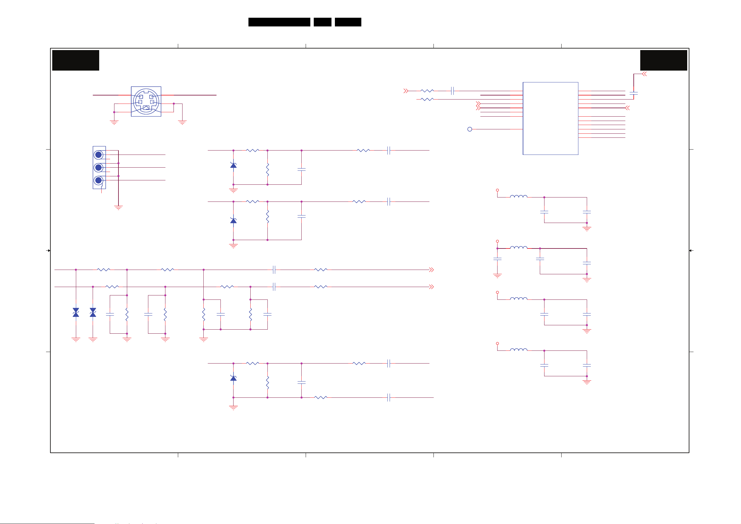
Circuit Diagrams and PWB Layouts
Scaler (19"): SCART connector
5
21TPM1.3E LA 7.
4
3
2
1
SB04 SB04
C113
C113
560pF
D
C C
560pF
SCART CONNECTOR
C115
C115
560pF
560pF
SCT1_AUR_IN
SCT1_AUL_IN
SCT1_FS_IN
SCT1_FB_IN
SCT1_AV_IN
CN102
CN102
SCT1_AUR_OUT
2
4
6
8
10
12
14
16
18
20
1
3
5
7
9
11
13
15
17
19
21
SCART
SCART
SCT1_AUL_OUT
SCT1_B_IN
SCT1_G_IN
SCT1_R_IN
SCT1_AVO_GND
SCT1_AV_OUT
Full SCART
SCT1_FB_IN
ZD109
ZD109
R155
R155
0 OHM 1/10W
0 OHM 1/10W
R157
R157
75 OHM 1/10W
75 OHM 1/10W
C112
C112
1000pF/25V
1000pF/25V
SCT1_AV_OUT 18
SOY0 4
C110
C110
1000pF/25V
1000pF/25V
SCT1_AUR_OUT 16
SCT1_AUL_OUT 16
SCT1_AVO_GND 18
SCT1_AV_IN
SCT1_G_IN
SCT1_B_IN
SCT1_R_IN
LRAEN
R142 27 OHM 1/10WR142 27 OHM 1/10W
ZD105
ZD105
UDZSNP5.6B
UDZSNP5.6B
L105
L105
1 2
80 OHM
80 OHM
ZD106
ZD106
UDZSNP5.6B
UDZSNP5.6B
L106
L106
1 2
80 OHM
80 OHM
ZD107
ZD107
UDZSNP5.6B
UDZSNP5.6B
ZD108
ZD108
L107
L107
1
UDZSNP5.6B
UDZSNP5.6B
80 OHM
80 OHM
2
Change to 75 OHM 1/8W
R144
R144
47 OHM 1/10W
47 OHM 1/10W
R147
R147
75 OHM 1/8W
75 OHM 1/8W
R151
R151
75 OHM 1/8W
75 OHM 1/8W
R154
R154
75 OHM 1/8W
75 OHM 1/8W
C139
C139
47pF
47pF
R145
R145
0 OHM 1/10W
0 OHM 1/10W
C142
C142
15pF/50V
15pF/50V
R148
R148
0 OHM 1/10W
0 OHM 1/10W
C145
C145
15pF/50V
15pF/50V
R152
R152
0 OHM 1/10W
0 OHM 1/10W
C147
C147
15pF/50V
15pF/50V
R143
R143
100 OHM 1/10W
100 OHM 1/10W
R146
R146
68 OHM 1/10W
68 OHM 1/10W
R149
R149
100 OHM 1/10W
100 OHM 1/10W
R150
R150
68 OHM 1/10W
68 OHM 1/10W
R153
R153
100 OHM 1/10W
100 OHM 1/10W
R156
R156
68 OHM 1/10W
68 OHM 1/10W
R215
R215
100 OHM 1/10W
100 OHM 1/10W
CI YLRAENROTCENNOC Y
C138 0.047uFC138 0.047uF
C140 1uF/16VC140 1uF/16V
C141 0.01uF/25VC141 0.01uF/25V
C143 0.01uF/25VC143 0.01uF/25V
C144 0.01uF/25VC144 0.01uF/25V
C146 0.01uF/25VC146 0.01uF/25V
C148 0.01uF/25VC148 0.01uF/25V
C134 0.047uFC134 0.047uF
SY0 5
GND_SV5
Y0P 4
Y0N 4
PB0P 4
PBR0N 4
PR0P 4
SC0 5
C146 C2 R240 A2
C143 C2 R150 C2
R153 C2 C204 A2
C139 D3 R160 B1
C144 C2 C205 A2
R142 D3 C206 A2
C112 D4 R149 C2
C148 B2 R156 B2
R151 C3 C115 D5
R238 B3 L105 D3
R236 B2 C149 B2
L106 C3 C110 D4
C147 C3 R234 A3
R154 C3 R148 C3
R152 C3 C113 D5
R161 B5 R239 B3
ZD106 C3 ZD132 B3
R157 B5 R235 A2
C140 D2 CN102 D5
R146 D2 R147 C3
ZD133 B3 R145 D3
L107 B3 C134 B2
R237 B2 C150 B2
R155 B5 ZD108 C3
ZD105 D3 C141 D2
ZD109 B5 R215 B2
R143 D2 R144 D3
R241 A2 C145 C3
ZD107 C3 C142 C3
R158 B5 C207 A3
ZD110 B5 C138 D2
R159 B1
D
UDZSNP5.6B
B
SCT1_FS_IN
A A
5
UDZSNP5.6B
R158
R158
33K OHM 1/10W
33K OHM 1/10W
ZD110
ZD110
RLZ13B
RLZ13B
1 2
R161
R161
10K OHM 1/10W
10K OHM 1/10W
SCART_FS_IN 9
4
SCT1_AUR_IN
SCT1_AUL_IN
R238 1K OHM 1/10WR238 1K OHM 1/10W
R239 1K OHM 1/10WR239 1K OHM 1/10W
ZD132
ZD132
ZD133
1 2
VPORT0603100KV05
VPORT0603100KV05
ZD133
VPORT0603100KV05
VPORT0603100KV05
1 2
3
C207 NC/470pFC207 NC/470pF
R236
R236
3K OHM 1/10W
3K OHM 1/10W
C206 NC/470pFC206 NC/470pF
R234
R234
100K OHM 1/10W
100K OHM 1/10W
R235
R235
100K OHM 1/10W
100K OHM 1/10W
R237
R237
3K OHM 1/10W
3K OHM 1/10W
C205 33pFC205 33pF
30K OHM 1/10W
30K OHM 1/10W
R241
R241
2
C204 33pFC204 33pF
30K OHM 1/10W
30K OHM 1/10W
R240
R240
NEARLY MT5335
C149 2.2uF/16VC149 2.2uF/16V
C150 2.2uF/16VC150 2.2uF/16V
R159
R159
20K OHM 1/10W
20K OHM 1/10W
R160
R160
20K OHM 1/10W
20K OHM 1/10W
AIN3_R 10
AIN3_L 10
1
I_17780_014.eps
170408
B
Page 22
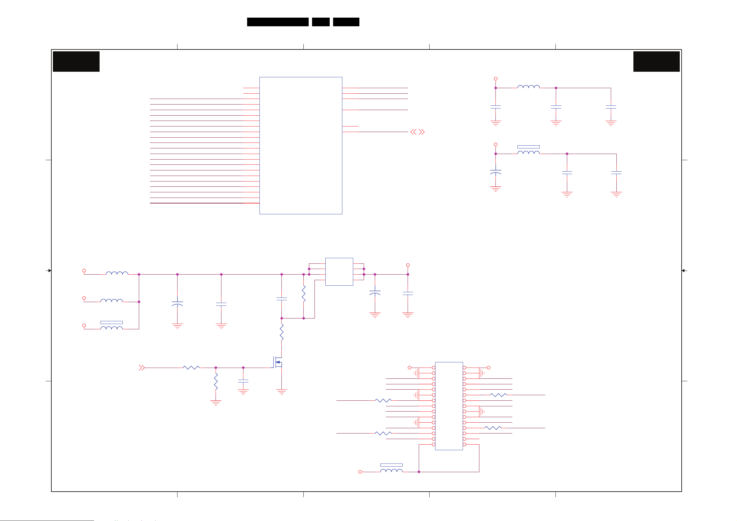
Scaler (19"): LVDS OUT
5
Circuit Diagrams and PWB Layouts
22TPM1.3E LA 7.
4
3
2
1
SB05
U401C
U401C
244
A0N
243
A0N
D
C C
A0P
A1N
A1P
A2N
A2P
CK1N
CK1P
A3N
A3P
A4N
A4P
A5N
A5P
A6N
A6P
CK2N
CK2P
A7N
A7P
242
241
240
239
237
236
235
234
233
232
231
230
228
227
226
225
224
223
222
221
A0P
A2N
A2P
CK1N
CK1P
A3N
A3P
A4N
A4P
A5N
A5P
A6N
A6P
A7N
A7P
CK2N
CK2P
A8N
A8P
A9N
A9P
MT5335PGU
MT5335PGU
AVD D33_LVDSA
AVD D33_LVDSB
AVD D33_LVDSC
AVD D33_VPLL
TP2
TN2
220
229
238
217
218
219
AVDD33_LVDS
AVDD33_LVDS
AVDD33_LVDS
AVDD33_VPLL
CI_POCE1# 20
AV33
AV33
+
+
FB301
FB301
BEAD
BEAD
C303
C303
1uF/16V
1uF/16V
FB302
FB302
1 2
BEAD
BEAD
C305
C305
100uF/16V
100uF/16V
AVD D33_LVDS
C302
C302
10uF/10V
10uF/10V
AVD D33_VPLL
C306
C306
1uF/16V
1uF/16V
SB05
C304
C304
0.1UF16V
0.1UF16V
C307
C307
0.1UF16V
0.1UF16V
LVDS OUT
D
U301
DV33
16V
+5V
B
3A
L301NCL301
NC
L302NCL302
NC
1 2
L303
L303
BEAD
BEAD
+
+
HI = > LVDS POWER ON
LVDS OUT
C310
C310
220uF/16V
220uF/16V
C311
C311
0.1UF16V
0.1UF16V
C312
C312
NC/1uF/16V
NC/1uF/16V
R302
R302
100K OHM 1/10W
100K OHM 1/10W
R305
R305
10K OHM 1/10W
10K OHM 1/10W
U301
1
S
2
3
4
AO4449 -7A/-30V
AO4449 -7A/-30V
D
S
D
D
S
G
D
8
7
6
5
+
+
C308
C308
NC/100uF/16V
NC/100uF/16V
LV DSVDD
C309
C309
0.1UF16V
0.1UF16V
LO = > LVDS POWER OFF
Q301
LV DSVDD_EN9
A
R306 51K OHM 1/10WR306 51K OHM 1/10W
R307
1M OHM 1/10W
1M OHM 1/10W
R307
C301
C301
1uF6.3V
1uF6.3V
Q301
2N7002 SOT-23
2N7002 SOT-23
CK1P
CK2P
R308 22 OHM 1/10WR308 22 OHM 1/10W
LV DSVDD LV DSVDD
A0N A0P
A1N A1P
A2N A2P
A3P
A4P
A5N
FB303
FB303
A6P
A7P
R310 22 OHM 1/10WR310 22 OHM 1/10W
CN301
CN301
1 2
3 4
5 6
7 8
9 10
11
13
15
17 18
19 20
21
23 24
25
27 28
29
CONN
CONN
R309 22 OHM 1/10WR309 22 OHM 1/10W
12
14
16
22
R311 22 OHM 1/10WR311 22 OHM 1/10W
26
30
A3N
A4N
A5P
A6N
A7N
CK1N
CK2N
R311 A2 R310 A3
FB301 D2 FB302 D2
CN301 B2 C302 D2
L303 B5 C303 D2
L302 B5 C308 B3
Q301 B4 U301 C3
C304 D1 C305 C2
C311 B4 C310 B5
R302 B4 C307 C1
R305 B4 L301 C5
C301 B4 U401 D4
C312 B4 C306 C2
R306 B4 R309 A2
R307 B4 R308 A3
C309 B3 FB3
03 A3
B
A
DV33
5
4
1 2
NC/220 OHM
NC/220 OHM
3
I_17780_015.eps
2
1
170408
Page 23
Circuit Diagrams and PWB Layouts
C
C
C
F
F
C
C
C
C
F
C
C
R
C
C
F
U
C
U
U
C
C
F
C
C
F
C
C
C
B
Scaler (19"): MT5335 HDMI/PLL
5
23TPM1.3E LA 7.
4
3 2
1
SB06 S
MT5335 HDMI/PLL
U401D
USB_VRT
12
12
D
USB_DUSB_D+
USB_DUSB_D+
AVDD33_USB
AVDD12_USB
TP409TP409
TP410TP410
U401D
68
65
66
67
69
157
158
MT5335PGU
MT5335PGU
USB_VRT
USB_DM
USB_DP
AVDD33_USB
AVDD12_USB
TP0
TN0
AVDD12_TVDPLL
AVDD12_SYSPLL
AVDD12_DTDPLL
AVDD12_ADCPLL
AVDD12_HDMIPLL
AVDD12_APLL
AVDD12_DMPLL
160
155
153
161
159
156
154
AVDD12_PLL
AVDD12_PLL
AVDD12_PLL
AVDD12_PLL
AVDD12_PLL
AVDD12_PLL
AVDD12_PLL
AV12
AV33
FB411
FB411
BEAD
BEAD
C502
C502
1uF/16V
1uF/16V
FB401
FB401
BEAD
BEAD
AVDD12_PLL
C503
C503
4.7uF/10V
4.7uF/10V
AVD D33_USB
C504
C504
0.01uF/25V
0.01uF/25V
C505
C505
0.1UF16V
0.1UF16V
USB_VRT
R470 5.1K OHM 1/10WR470 5.1K OHM 1/10W
01/18 Modify
C506
C506
4.7uF/10V
4.7uF/10V
C507
C507
0.1UF16V
0.1UF16V
AV12
C
FB412
FB412
BEAD
BEAD
C508
C508
10uF/10V
10uF/10V
AVDD12_USB
C509
C509
4.7uF/10V
4.7uF/10V
C510
C510
0.1UF16V
0.1UF16V
AV25
FB413
FB413
BEAD
BEAD
AVD D25 _SADC
U401H
U401H
C511
C511
1uF/16V
1uF/16V
C512
C512
4.7uF/10V
4.7uF/10V
AVSS25_SADC
C513
C513
0.01uF/25V
0.01uF/25V
C514
C514
0.1UF16V
0.1UF16V
AVDD25_SADC
AVDD25_SADC
AVSS25_SADC
RF_AGC
IF_AGC
TP411TP411
164
166
167
195
194
MT5335PGU
MT5335PGU
SIFP
SIFN
AF
TUNER_DATA
TUNER_CLK
18
18
B
20
TS_VALIDO20
TS_CKO
MPX0P
MPX0N
163
AVSS25_SADC
165
193
192
TS_DATAO 20
TS_SYNCO 20
AV33
C517
C517
1uF/16V
1uF/16V
FB414
FB414
BEAD
BEAD
AVD D33_H
C515
C515
4.7uF/10V
4.7uF/10V
C516
C516
0.1UF16V
0.1UF16V
U401K
U401K
15
15
15
15
15
A
RX0_CB
RX0_C
RX0_0B15
RX0_015
RX0_1B
RX0_115
RX0_2B
RX0_2
RX0_CB
RX0_C
RX0_0B
RX0_0
RX0_1B
RX0_1
RX0_2B
RX0_2
79
RX0_CB
80
RX0_C
81
RX0_0B
82
RX0_0
83
RX0_1B
84
RX0_1
85
RX0_2B
86
RX0_2
MT5335PGU
MT5335PGU
EXT_RES
OPWR0_5V
AVDD33_HDMI
AVDD12_CVCC
77
73
AVDD33_H
78
AVDD12_CVCC
74
TP401TP401
HDMI_5V
AV12
C518
C518
1uF/16V
1uF/16V
FB415
FB415
BEAD
BEAD
AVDD12_CVCC
C519
C519
4.7uF/10V
4.7uF/10V
C520
C520
0.1UF16V
0.1UF16V
Page 24
Circuit Diagrams and PWB Layouts
0
0
8
B
B
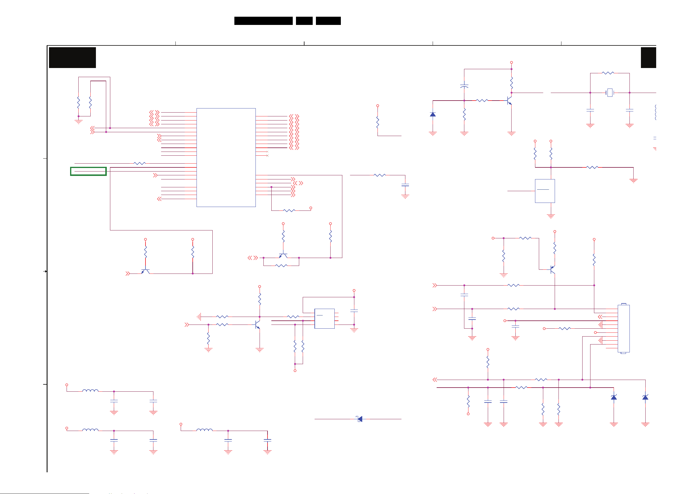
Scaler (19"): MT5335 Control/IR/LED
5
24TPM1.3E LA 7.
4 3 2 1
SB07 S
MT5335 CONTROL/IR/LED/KEY
C488
C488
+
+
220uF/10V
220uF/10V
R449
R449
220 OHM 1/10W
D
OSDA013,19
R492
R492
R493
R493
4.7K OHM 1/10W
4.7K OHM 1/10W
4.7K OHM 1/10W
4.7K OHM 1/10W
BL_DIM21
OPWM120
KEY2
KEY1_MT5335
C
10K OHM 1/10W
10K OHM 1/10W
HDMI_INT13
B
OSCL013,19
15
OSDA1
15
OSCL1
OPWM212,20
MTK_IC_RESET20
R488 33 OHM 1/10WR488 33 OHM 1/10W
SCART_FS_IN6
POWER_ON/OFF21
+3V3SB +3V3SB
R444
R444
OSDA0
OSCL0
OXTALO
OXTALI
AVC C_SRV
AVD D33_XTAL
PWRDET
AVD D33_REG
C_XREG
ORESET#
10K OHM 1/10W
10K OHM 1/10W
Q403
Q403
MMBT3904
MMBT3904
EDID_PRT
R445
R445
204
205
191
202
203
146
143
144
147
145
152
151
150
149
148
63
62
88
87
71
72
U401B
U401B
OSDA0
OSCL0
OSDA1
OSCL1
OPWM0
OPWM1
OPWM2
VCXO
XTALO
XTALI
AVD D33_SRV
AVD D33_XTAL
ADIN4
ADIN3
ADIN2
ADIN1
ADIN0
AVD D33_REG
C_XREG
ORESET_
OPWRSB
MT5335PGU
MT5335PGU
R420
R420
NC/0 OHM 1/10W
NC/0 OHM 1/10W
R461 10K OHM 1/10WR461 10K OHM 1/10W
R463
R463
10K OHM 1/10W
10K OHM 1/10W
GPIO_3
GPIO_4
GPIO_5
GPIO_6
GPIO_7
GPIO_8
GPIO_9
GPIO_10
GPIO_11
GPIO_12
GPIO_13
OPCTRL0
OPCTRL1
OPCTRL2
OPCTRL3
OPCTRL4
OPCTRL5
CEC13,14
R456
10K OHM 1/10W
10K OHM 1/10W
R456
207
208
209
59
60
210
211
212
214
215
216
92
91
76
75
90
89
DV33
Q406
Q406
MMBT3904
MMBT3904
R426
R426
4.7K OHM 1/10W
4.7K OHM 1/10W
+3V3SB
R486NCR486
NC
R495
R495
0 OHM 1/10W
0 OHM 1/10W
R459
R459
33 OHM 1/10W
33 OHM 1/10W
OSCL0
OSDA0
CI_PDD3 20
CI_PDD4 20
CI_PDD5 20
CI_PDD6 20
CI_PDD7 20
CI_POWE# 20
CI_OEB 20
CI_ALE 20
CI_CLE 20
LVD SVDD_EN 7
CI_INT 20
AMP_MUTE 17
BL_ON/OFF 21
EDID_PRT
+3V3SB
Q408
Q408
NC/MMBT3904
NC/MMBT3904
8
7
6
5
+3V3SB
R487NCR487
NC
U405
U405
VCC
WC
SCL
SDA
M24C16
M24C16
IIC ADDRESS "A0"
NC
NC
NC
VSS
1
2
3
4
C_XREG
The divider only for A version IC
DV33
DV33
R448
R448
1K OHM 1/10W
1K OHM 1/10W
PWRDET
R454 1 OHM +-5% 1/10WR454 1 OHM +-5% 1/10W
C492
C492
1uF/16V
1uF/16V
C491
C491
4.7uF/10V
4.7uF/10V
TURN_ON13
STANDBY13
D401
D401
LL4148
LL4148
TURN_ON
STANDBY
1/8 River
220 OHM 1/10W
R450
R450
47K OHM 1/10W
47K OHM 1/10W
Adjust the power on timing
+5V
C441
C441
1000pF/25V
1000pF/25V
C452
C452
1000pF/25V
1000pF/25V
+3V3SB_uP
For OTS
+3V3SB_uP
+3V3SB
R427
R427
R453
R453
0 OHM 1/10W
0 OHM 1/10W
R455
R455
0 OHM 1/10W
0 OHM 1/10W
C493
C493
4.7uF/10V
4.7uF/10V
R447
R447
1K OHM 1/10W
1K OHM 1/10W
ORESET#
Q404
Q404
MMBT3904
MMBT3904
+3V3SB +5VSB
ORESET#
R462
R462
NC/1K OHM 1/10W
NC/1K OHM 1/10W
NC/3K OHM 1/10W
NC/3K OHM 1/10W
2
+5VSB
OXTAL I
Third-Tone Crystal
R498
R498
R497NCR497
NC/6.2K OHM 1/10W
NC/6.2K OHM 1/10W
NC
3
U408
U408
NC/MAX809STRG
NC/MAX809STRG
VCC
RESET
GND
1
+3V3SB_uP
R460
NC/1K OHM 1/10W
R460
NC/1K OHM 1/10W
Q405
Q405
NC/MMBT3906
NC/MMBT3906
R452 NCR452 NC
R446 NCR446 NC
Y401
Y401
2
60MHz
60MHz
C489
C489
10pF
10pF
R499
R499
NC/13K OHM 1% 1/10W
NC/13K OHM 1% 1/10W
+5V
R428
NC/1K OHM 1/10W
R428
NC/1K OHM 1/10W
OIRI12,13
+3V3SB_uP
TXC
1
CN404
CN404
1
2
3
4
5
6
7
8
9
10
11
OXTAL O
C490
C490
10pF
10pF
Q403
R464
FB41
R489
ZD41
FB40
C489
C452
C495
U408
C441
R427
C490
R488
C401
C496
R493
R458
D403
R492
C498
R449
Q404
R498
R462
C488
R499
Q405
R453
R445
U405
R448
C497
R446
R486
Q408
Y401
CONN
CONN
R464
R464
R465
R465
4.7K OHM 1/10W
4.7K OHM 1/10W
4.7K OHM 1/10W
4.7K OHM 1/10W
DV33
+3V3SB
+3V3SB
A
FB408
FB408
BEAD
BEAD
FB410
FB410
BEAD
BEAD
AVC C_SRV
C494
C494
1uF/16V
1uF/16V
AVD D33_XTAL
C500
C500
1uF/16V
1uF/16V
C495
C495
0.1UF16V
0.1UF16V
C501
C501
0.1UF16V
0.1UF16V
+3V3SB
FB409
FB409
BEAD
BEAD
AVD D33_REG
C498
C498
1uF/16V
1uF/16V
C499
C499
0.1UF16V
0.1UF16V
D403
D403
SCS140V
SCS140V
12
13
KEY1KEY1_MT5335
1/3 River
KEY1
KEY1
KEY2
R458NCR458
NC
+3V3SB_uP
R489NCR489
NC
C496
C496
1000pF
1000pF
R466 100 OHM 1/10WR466 100 OHM 1/10W
R467
R467
100 OHM 1/10W
100 OHM 1/10W
C497
C497
1000pF
1000pF
470K OHM 1/10W
470K OHM 1/10W
R468
R468
R469
R469
100K OHM 1/10W
100K OHM 1/10W
ZD410
ZD410
NC/UDZSNP5.6B
NC/UDZSNP5.6B
1 2
ZD411
ZD411
NC/UDZSNP5.6
NC/UDZSNP5.6
1 2
Page 25

Circuit Diagrams and PWB Layouts
Scaler (19"): MT5335 Audio In/Out
5
25TPM1.3E LA 7.
4
3
2
1
SB08 SB08
D
MT5335 AUDIO IN/OUT
AIN0_L3
3
4
AIN0_R
AIN1_L
AIN1_R4
AIN2_L5
AIN2_R5
AIN3_L6
AIN3_R6
AVDD33_AADC
AVSS33_AADC
VIMD_AADC
REFP_AADC
REFN_AADC
177
176
175
174
173
172
171
170
169
181
179
180
178
U401G
U401G
AIN0_L
AIN0_R
AIN1_L
AIN1_R
AIN2_L
AIN2_R
AIN3_L
AIN3_R
AVD D33_AADC
AVSS33_AADC
VMID_AADC
REFP_AADC
REFN_AADC
MT5335PGU
MT5335PGU
ASPDIF
AOMCLK
AOLRCK
AOBCK
AOSD ATA0
AL1
AR1
AL2
AR2
AVDD 33_ADAC0
AVSS33_ADAC0
AVSS33_ADAC1
AVDD 33_ADAC1
ADAC_VCM
AVD D33_DIG
201
AOMCLK
198
AOLRCK
199
AOBCK
200
MT5133_RESET
196
186
185
189
187
AVDD33_ADAC0
190
AVDD33_ADAC1
182
AVSS33_ADAC0
188
AVSS33_ADAC1
184
ADAC_VCM
183
AVDD33_DIG
168
ASPDIF 4
AOLRCK 12
AOBCK 12
MT5133_RESET 19
AL1O 16
AR1O 16
AL2O 16
AR2O 16
TP402TP402
ADAC_VCM
C472
C472
+
+
10uF/16V
10uF/16V
C473
C473
0.1UF16V
0.1UF16V
FB403 C4
C479 B3
FB404 C3
C483 B3
C476 B3
C484 A4
C C
C481 B2
C474 C4
C477 B2
FB407 A4
C482 B4
AV33
B
AV33
C474
C474
+
+
100uF/16V
100uF/16V
FB403
FB403
BEAD
BEAD
FB406
FB406
BEAD
BEAD
AVDD33_AADC
C475
C475
1uF/16V
1uF/16V
AVSS33_AADC
REFP_AADC
C476
C476
0.1UF16V
0.1UF16V
AV33
AV33
FB404
FB404
BEAD
BEAD
FB405
FB405
BEAD
BEAD
AVDD33_ADAC1
C477
C477
1uF/16V
1uF/16V
AVSS33_ADAC1
AVDD33_DIG
C478
C478
0.1UF16V
0.1UF16V
C475 B4
C485 A3
U401 D4
C473 D2
C478 B2
C487 A2
C480 B2
FB406 B4
FB405 B3
C486 A3
C472 D2
D
B
C479
C479
4.7uF/10V
C483
C482
C482
1uF/16V
1uF/16V
REFN_AADC
AV33
A
5
FB407
FB407
BEAD
BEAD
4
AVDD33_ADAC0
C484
C484
1uF/16V
1uF/16V
AVSS33_ADAC0
C483
0.1UF16V
0.1UF16V
C485
C485
0.1UF16V
0.1UF16V
3
4.7uF/10V
VIMD_AADC
C486
C486
4.7uF/10V
4.7uF/10V
C480
C480
1uF/16V
1uF/16V
AVSS33_DIG
C487
C487
0.1UF16V
0.1UF16V
2
C481
C481
0.1UF16V
0.1UF16V
A
I_17780_018.eps
1
170408
Page 26

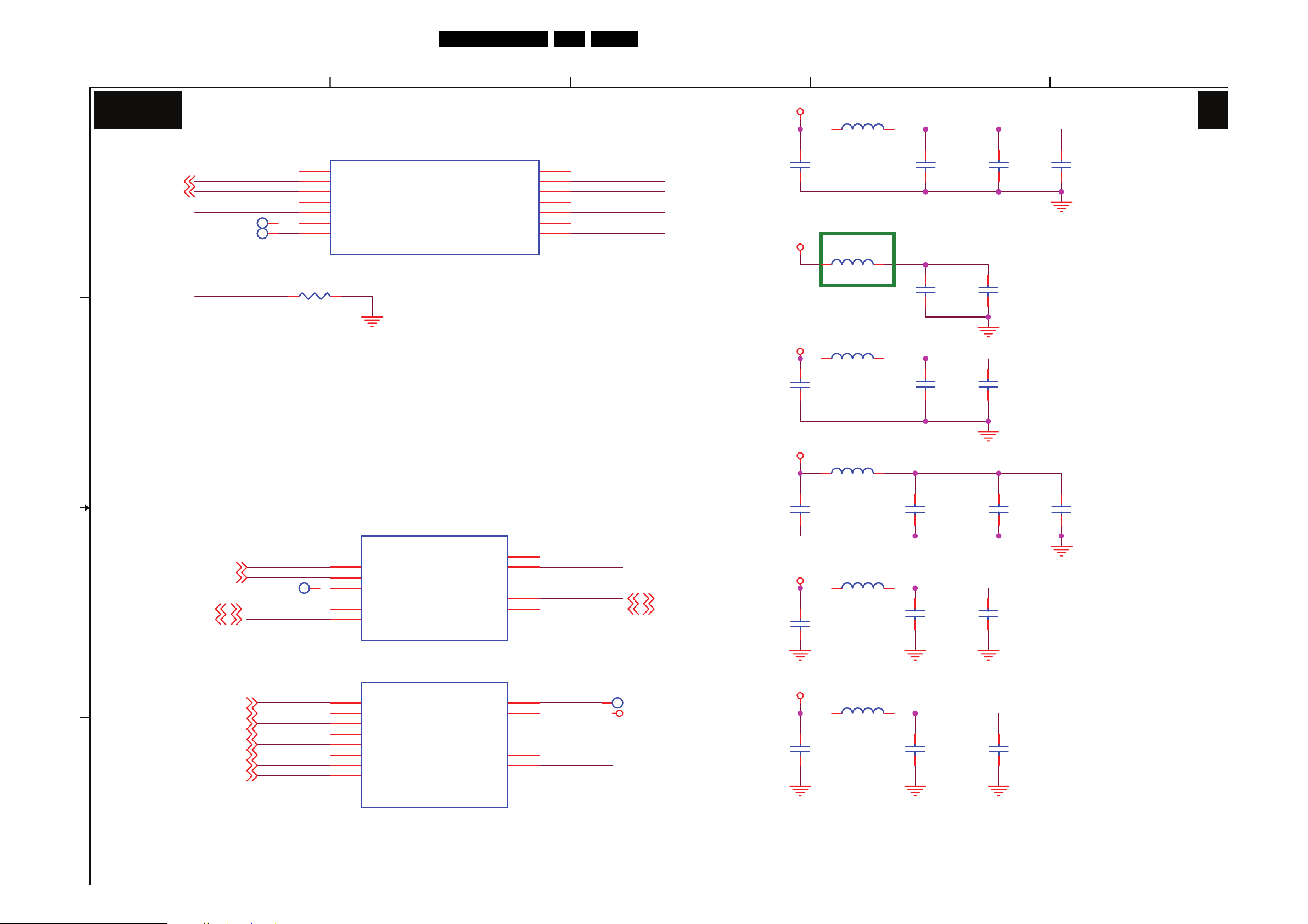
Circuit Diagrams and PWB Layouts
26TPM1.3E LA 7.
Scaler (19"): DDR1 MEMORY
5
4
3
2
1
DDR1 MEMORY
SB09
RDQS0
RDQM0
RDQ0
RDQ1
RDQ2
RDQ3
RDQ4
RDQ5
RDQ6
D
C C
DDRV
+
+
RDQ7
RDQS1
RDQM1
RDQ8
RDQ9
RDQ10
RDQ11
RDQ12
RDQ13
RDQ14
RDQ15
MEM_VREF
RCS#
MEM_ADDR12
MEM_ADDR11
MEM_ADDR9
MEM_ADDR7
MEM_ADDR6
MEM_ADDR5
MEM_ADDR4
MEM_WE# RWE#
MEM_CAS#
MEM_RAS#
MEM_CS#
MEM_BA0
MEM_BA1
MEM_ADDR10
MEM_ADDR1
MEM_ADDR2
MEM_ADDR3
C440
C433
C433
100uF/16V
100uF/16V
C440
4.7uF/10V
4.7uF/10V
U401A
U401A
11
RDQS0
13
RDQM0
9
RDQ0
8
RDQ1
7
RDQ2
6
RDQ3
5
RDQ4
4
RDQ5
3
RDQ6
2
RDQ7
17
RDQS1
15
RDQM1
19
RDQ8
20
RDQ9
21
RDQ10
22
RDQ11
23
RDQ12
24
RDQ13
25
RDQ14
26
RDQ15
53
RVRE F0
46
RCS_
MT5335PGU
MT5335PGU
RN406 47 OHM 1/16WRN406 47 OHM 1/16W
5
6
7
8
RN408 47 OHM 1/16WRN408 47 OHM 1/16W
5
6
7
8
RN409 47 OHM 1/16WRN409 47 OHM 1/16W
5
6
7
8
RN410 47 OHM 1/16WRN410 47 OHM 1/16W
5
6
7
8
RN415 47 OHM 1/16WRN415 47 OHM 1/16W
5
6
7
8
RCLK0_
4
3
2
1
4
3
2
1
4
3
2
1
4
3
2
1
4
3
2
1
Add serial resistors for DRAM
FB416 BEADFB416 BEAD
C448
C435
C435
0.1UF16V
0.1UF16V
C448
0.01uF/25V
0.01uF/25V
RA0
RA7
RWE_
RBA0
RA6
RBA1
RA5
RRAS_
RA8
RA10
RA4
RCAS_
RA12
RCKE
RA11
RA9
RA3
RA1
RA2
RCLK0
47
36
40
43
37
44
38
42
35
45
39
41
32
31
33
34
51
49
50
28
29
C434
C434
0.1UF16V
0.1UF16V
RA0
RA7
RWE#
RBA0
RA6
RBA1
RA5
RRAS#
RA8
RA10
RA4
RCAS#
RA12
RCKE
RA11
RA9
RA3
RA1
RA2
RCLK0#
RCLK0
RA12
RA11
RA9
RA8MEM_ADDR8
RA7
RA6
RA5
RA4
RCAS#
RRAS#
RCS#
RBA0
RBA1
RA10
RA0MEM_ADDR0
RA1
RA2
RA3
C437
C437
0.1UF16V
0.1UF16V
U402A
12/6 Modify
MEM_ADDR12
MEM_ADDR11
MEM_ADDR10
MEM_ADDR9
MEM_ADDR8
MEM_ADDR7
MEM_ADDR6
MEM_ADDR5
MEM_ADDR4 MEM_DQ7
MEM_ADDR3
MEM_ADDR2
MEM_ADDR1
MEM_ADDR0
MEM_BA1
MEM_BA0
MEM_RAS#
MEM_CAS#
MEM_WE#
MEM_DQM1
MEM_DQM0
MEM_CLK0#
MEM_CLK0
MEM_CLKEN
RCKE
RCLK0
RCLK0#
C951
C438
C438
0.1UF16V
0.1UF16V
C951
0.1UF16V
0.1UF16V
U402A
DDR SDRAM
DDR SDRAM
42
RES(A12)
41
A11
28
A10
40
A9
39
A8
38
A7
37
A6
36
A5
35
A4
32
A3
31
A2
30
A1
29
A0
27
BA1
26
BA0
23
RAS
22
CAS
21
WE
47
UDM
20
LDM
46
CK
45
CK
44
CKE
HY5DU121622DTP-D43
HY5DU121622DTP-D43
R432
R432
22 OHM 1/10W
22 OHM 1/10W
R433
R433
22 OHM 1/10W
22 OHM 1/10W
R439
R439
22 OHM 1/10W
22 OHM 1/10W
DDRV_BEAD1
C449
C449
0.01uF/25V
0.01uF/25V
DQ0
DQ1
DQ2
DQ3
DQ4
DQ5
DQ6
DQ7
DQ8
DQ9
DQ10
DQ11
DQ12
DQ13
DQ14
DQ15
UDQS
LDQS
CS
MEM_CLK0
MEM_CLK0#
2
4
5
7
8
10
11
13
54
56
57
59
60
62
63
65
51
16
24
DDR#1
MEM_CLKEN
MEM_VREF
C443
C443
0.1UF16V
0.1UF16V
MEM_DQ0
MEM_DQ1
MEM_DQ2
MEM_DQ3
MEM_DQ4
MEM_DQ5
MEM_DQ6
MEM_DQ8
MEM_DQ9
MEM_DQ10
MEM_DQ11
MEM_DQ12
MEM_DQ13
MEM_DQ15
MEM_DQ14
MEM_DQS1
MEM_DQS0
MEM_CS#
R434
R434
100 OHM 1/10W
100 OHM 1/10W
MEM_VREF
C444
C444
0.1UF16V
0.1UF16V
MEM_ADDR13
MEM_VREF
Swap for layout
C445
C445
4.7uF/10V
4.7uF/10V
U402B
U402B
DDR SDRAM
DDR SDRAM
(PWR)
(PWR)
14
NC1
17
NC2
19
NC3
25
NC4
43
NC5
50
NC6
53
NC7
49
VREF
HY5DU121622DTP-D43
HY5DU121622DTP-D43
12/12 Modify
+1V3D
C457
C457
0.1UF16V
0.1UF16V
VDD1
VDD2
VDD3
VDDQ1
VDDQ2
VDDQ3
VDDQ4
VDDQ5
VSS1
VSS2
VSS3
VSSQ1
VSSQ2
VSSQ3
VSSQ4
VSSQ5
C458
C458
0.1UF16V
0.1UF16V
MEM_WE#
MEM_CAS#
DDRV_BEAD1
1
18
33
3
9
15
55
61
34
48
66
6
12
52
58
64
DDRV
DDRV_BEAD1
DDRV_BEAD2
12/12 Modify
75 OHM/NC
75 OHM/NC
RDQ0
RN411 47 OHM 1/16WRN411 47 OHM 1/16W
RDQ1
RDQ2
RDQ3
RDQ4
RDQ5
RDQ6
RDQ7
RDQS0
RDQM0
RDQM1
RDQS1
RDQ8
RDQ9
RDQ10
RDQ11 MEM_DQ11
RDQ12
RDQ13
RDQ14
RDQ15
5
6
7
8
RN413 47 OHM 1/16WRN413 47 OHM 1/16W
5
6
7
8
R435 47 OHM 1/16WR435 47 OHM 1/16W
R437 47 OHM 1/16WR437 47 OHM 1/16W
R440 47 OHM 1/16WR440 47 OHM 1/16W
R442 47 OHM 1/16WR442 47 OHM 1/16W
RN416 47 OHM 1/16WRN416 47 OHM 1/16W
8
7
6
5
RN418 47 OHM 1/16WRN418 47 OHM 1/16W
8
7
6
5
4
3
2
1
4
3
2
1
1
2
3
4
1
2
3
4
MEM_DQ14
MEM_DQ15
MEM_RAS#
MEM_CS#
MEM_BA0
MEM_BA1
MEM_ADDR10
+1V3D
MEM_ADDR4
MEM_ADDR5
MEM_ADDR6
MEM_ADDR7
MEM_CLKEN
MEM_ADDR12
MEM_ADDR11
MEM_ADDR9
MEM_ADDR8
MEM_ADDR0
MEM_ADDR1
MEM_ADDR2
MEM_ADDR3
MEM_ADDR13
MEM_DQ0
MEM_DQ1
MEM_DQ2
MEM_DQ3
MEM_DQ4
MEM_DQ5
MEM_DQ6
MEM_DQ7
MEM_DQS0
MEM_DQM0
MEM_DQM1
MEM_DQS1
MEM_DQ8
MEM_DQ9
MEM_DQ10
MEM_DQ12
MEM_DQ13
Swap for layout
C462
C459
C459
0.1UF16V
0.1UF16V
C460
C460
0.1UF16V
0.1UF16V
C461
C461
0.1UF16V
0.1UF16V
C462
0.1UF16V
0.1UF16V
RN402 8P4R 75 OHM +-5% 1/16WRN402 8P4R 75 OHM +-5% 1/16W
8
7
6
5
RN4038P4R 75 OHM +-5% 1/16WRN4038P4R 75 OHM +-5% 1/16W
8
7
6
5
RN404 8P4R 75 OHM +-5% 1/16WRN404 8P4R 75 OHM +-5% 1/16W
8
7
6
5
R430NCR430NC
RN405 8P4R 75 OHM +-5% 1/16WRN405 8P4R 75 OHM +-5% 1/16W
5
6
7
8
RN407 8P4R 75 OHM +-5% 1/16WRN407 8P4R 75 OHM +-5% 1/16W
8
7
6
5
R431NCR431NC
RN412 8P4R 75 OHM +-5% 1/16WRN412 8P4R 75 OHM +-5% 1/16W
RN414 8P4R 75 OHM +-5% 1/16WRN414 8P4R 75 OHM +-5% 1/16W
R436 75 OHM 1/10WR436 75 OHM 1/10W
R438 75 OHM 1/10WR438 75 OHM 1/10W
R441 75 OHM 1/10WR441 75 OHM 1/10W
R443 75 OHM 1/10WR443 75 OHM 1/10W
RN417 8P4R 75 OHM +-5% 1/16WRN417 8P4R 75 OHM +-5% 1/16W
RN419 8P4R 75 OHM +-5% 1/16WRN419 8P4R 75 OHM +-5% 1/16W
MEM_DQ15
MEM_DQ14
C463
C952
C952
0.1UF16V
0.1UF16V
C463
4.7uF/10V
4.7uF/10V
1
2
3
4
1
2
3
4
1
2
3
4
4
3
2
1
1
2
3
4
1
8
2
7
3
6
4
5
1
8
2
7
3
6
4
5
1
8
2
7
3
6
4
5
1
8
2
7
3
6
4
5
C447
C447
+
+
100uF/16V
100uF/16V
SB09
+1V3D
+1V3D
D
C439
C439
0.1UF16V
0.1UF16V
+
+
C7931
C7931
470uF/10V
470uF/10V
DDRV_BEAD2
C451
C451
0.01uF/25V
0.01uF/25V
Low ESR
C465
C465
0.1UF16V
0.1UF16V
VTT
C946
C946
0.1UF16V
0.1UF16V
MEM_VREF
C949
C948
C948
0.1UF16V
0.1UF16V
4
C949
1uF/16V
1uF/16V
2
R7928
R7928
110 OHM 1/10W
110 OHM 1/10W
R7930
R7930
120 OHM 1/10W
120 OHM 1/10W
FB417 BEADFB417 BEAD
C450
C450
0.01uF/25V
0.01uF/25V
C436
C436
0.1UF16V
0.1UF16V
DDRV
C936
C936
0.1UF16V
0.1UF16V
1.25 x (1+120/110) = 2.6V
B B
12/12 Modify
+5V
C942
C942
1uF/16V
1uF/16V
A A
IC G9084T43U TO-252
U909U909
VIN3VOUT
C943
C943
10uF/10V
10uF/10V
ADJ
1
+
+
C944
C944
22uF
22uF
5
C466
C466
0.1UF16V
0.1UF16V
+1V3DVTT
C467
C467
0.1UF16V
0.1UF16V
R931 4.7K OHM 1/10WR931 4.7K OHM 1/10W
U910
U910
1
GND
2
SD
3
VSENSE
VREF4VDDQ
3
C471
C471
4.7uF/10V
4.7uF/10V
VTT
PVIN
AVI N
HS
G2996F1Uf
G2996F1Uf
9
RN406 C5 U401 D5 RN402 D1
RN413 C2 C457 B3 C950 A3
R7930 A5 C439 B4 U402 D3
RN415 C5 RN408 C5 C448 B5
C443 B3 R437 C2 C451 B4
C436 B4 C466 B3 C458 B3
RN407 D1 C462 B2 RN411 C2
R438 C1 RN417 C1 C463 B1
RN416 C2 U909 B5 C434 B4
RN405 D1 RN404 D1 C440 B5
C943 A5 C7931 A4 FB417 B5
C952 B2 RN403 D1 R440 C2
R439 C4 C944 A5 C465 B3
C444 B3 C460 B2 RN418 C2
8
7
6
5
C950
C950
0.1UF16V
0.1UF16V
DDRV
2
RN412 C1 C942 A5 R432 C4
C445 B3 C449 B4 R430 D1
U402 D4 C435 B5 R441 C1
R435 C2 RN410 C5 C951 B4
RN414 C1 C447 B1 C467 B3
C433 B5 FB416 B5 C946 A3
C948 A3 RN419 C1 R434 C3
R931 A3 R431 D1 C936 A5
R7928 A5 C471 B3 R433 C4
C450 B5 C437 B4 R442 C2
RN409 C5 C461 B2 C949 A3
U910 A3 R443 C1 C459 B2
R436 C1 C438 B4
1
I_17780_019.eps
170408
Page 27

Circuit Diagrams and PWB Layouts
Scaler (19"): FLASH/JTAG/UART/IR
5
27TPM1.3E LA 7.
4
3
2
1
SB10
U401J
U401J
POCE0#
POOE#
PDD0
D
20
20
CI_RB
CI_PDD2
PDD1 OIRI_MT5335
12/12Modify
C
OIRI_MT5335
B B
A A
DV1 0
162
213
206
246
14
48
57
58
61
70
U401I
U401I
VCCK
VCCK
VCCK
VCCK
VCCK
DVDD10
DVDD10
VCCK
VCCK
VCCK
MT5335PGU
MT5335PGU
252
POCE0_
251
POOE_
250
PDD0
249
PDD1
245
PA RB _
248
PDD2
MT5335PGU
MT5335PGU
+3V3SB
R457
R457
10K OHM 1/10W
10K OHM 1/10W
R485 NC/0 OHM 1/10WR485 NC/0 OHM 1/10W
+3V3SB
U407
U407
5
VCC
4
Y
NC/SN74LVC1G08DCKR
NC/SN74LVC1G08DCKR
+3V3SB
VCC2IO
VCC2IO
VCC2IO
VCC2IO
VCC2IO
VCC2IO
VCC2IO
VCC2IO
VCC2IO
VCC2IO
VCC3IO_3
VCC3IO_3
VCC3IO_3
E-PAD
1
A
2
B
3
GND
Q407
Q407
2N7002 SOT-23
2N7002 SOT-23
10
12
16
18
27
30
52
54
55
56
64
197
247
257
DDRV
U0RX
U0TX
OIRI
JTMS
JTRST_
JTCK
JTDO
JTDI
DV33
95
94
93
253
1
256
255
254
DV33
U0RX
U0RX 3
U0TX
U0TX 3
JTMS
JTRST#
JTCK
JTDO
JTDI
OIRI
OIRI 9,13
R424
R424
4.7K OHM 1/10W
4.7K OHM 1/10W
OPWM2
AOBCK
AOLRCK
R421
R421
4.7K OHM 1/10W
4.7K OHM 1/10W
R423
R423
4.7K OHM 1/10W
4.7K OHM 1/10W
R425NCR425
NC
OPWM2 9,20
AOBCK 10
AOLRCK 10
Tr ap Mode
Normal mode
ICE mode
Tr ap Mode OPCTRL4
Core Reset 1 us
PDD1
PDD0
POOE#
POCE0#
FRESET#
R412
4.7K OHM 1/10W
4.7K OHM 1/10W
R412
USB_D-8
USB_D+8
DV33
R422
R422
10K OHM 1/10W
10K OHM 1/10W
OIRI
USB_DUSB_D+
AOLRCKAOBCKOPWM2
000
0
OPCTRL5
0(AMP_MUTE) 1 (HPDIN)
01
R411
R411
0 OHM 1/10W
0 OHM 1/10W
ZD402
ZD402
UDZSNP5.6B
UDZSNP5.6B
DV33
C406
C406
0.1UF16V
0.1UF16V
ZD408
ZD408
UDZSNP5.6B
UDZSNP5.6B
+5VSB
ZD404
ZD404
C407
C407
0.1UF16V
0.1UF16V
UDZSNP5.6B
UDZSNP5.6B
DV33
DV1 0
DDRV
15
8
16
7
9
1
14
2
C408
C408
0.1UF16V
0.1UF16V
C413
C413
4.7uF/10V
4.7uF/10V
C424
C424
4.7uF/10V
4.7uF/10V
U404
U404
SPI FLASH
SPI FLASH
32M bit
32M bit
D
Q
C
S
W
HOLD
NC8
Vcc
MX25L3205DMI-12G
MX25L3205DMI-12G
ZD403
ZD403
UDZSNP5.6B
UDZSNP5.6B
NC1
NC2
NC3
NC4
NC5
NC6
NC7
GND
CN405
CN405
1
2
3
4
5
CONN
CONN
C409
C409
0.1UF16V
0.1UF16V
C414
C414
1uF/16V
1uF/16V
C425
C425
1uF/16V
1uF/16V
3
4
5
6
11
12
13
10
4.7K OHM 1/10W
4.7K OHM 1/10W
C410
C410
0.1UF16V
0.1UF16V
I / O BYPASS
C415
C415
0.1UF16V
0.1UF16V
C426
C426
0.1UF16V
0.1UF16V
R414
R414
U0TX
U0RX
JTRST#
JTDI
JTMS
JTCK
JTDO
ZD407
ZD407
C411
C411
4.7uF/10V
4.7uF/10V
C416
C416
0.1UF16V
0.1UF16V
C427
C427
0.1UF16V
0.1UF16V
R482 33 OHM 1/10WR482 33 OHM 1/10W
R483 33 OHM 1/10WR483 33 OHM 1/10W
R491 33 OHM 1/10WR491 33 OHM 1/10W
R496 33 OHM 1/10WR496 33 OHM 1/10W
R416 33 OHM 1/10WR416 33 OHM 1/10W
+3V3SB
R415
R415
4.7K OHM 1/10W
4.7K OHM 1/10W
ZD409
ZD409
1/3 River
UDZSNP5.6B
UDZSNP5.6B
C412
C412
1uF/16V
1uF/16V
CN406
CN406
1
2
3
CONN
CONN
UDZSNP5.6B
UDZSNP5.6B
C417
C417
0.1UF16V
0.1UF16V
CORE BYPASS Near IC
C428
C428
0.1UF16V
0.1UF16V
DDR BYPASS Near IC
C418
C418
0.1UF16V
0.1UF16V
C429
C429
0.1UF16V
0.1UF16V
4
5
R417
R417
10K OHM 1/10W
10K OHM 1/10W
U0TX
U0RX
ZD406
ZD406
C419
C419
0.1UF16V
0.1UF16V
C430
C430
0.1UF16V
0.1UF16V
123
876
ZD405
ZD405
NC/UDZW5.6B
NC/UDZW5.6B
C420
C420
0.1UF16V
0.1UF16V
C431
C431
0.1UF16V
0.1UF16V
RN401
RN401
10KOHM +-5% 1/16W
10KOHM +-5% 1/16W
R418
R418
10K OHM 1/10W
10K OHM 1/10W
NC/UDZW5.6B
NC/UDZW5.6B
C421
C421
0.1UF16V
0.1UF16V
C432
C432
0.1UF16V
0.1UF16V
DV33
R413
R413
1K OHM 1/10W
1K OHM 1/10W
TVTREF#1
JTAG_DBGRQ
JTAG_DBGACK
R419
R419
10K OHM 1/10W
10K OHM 1/10W
CN407
CN407
1
2
3
NC/CONN
NC/CONN
C422
C422
0.1UF16V
0.1UF16V
CN401
CN401
2
4
6
8
10
12
14
16
18
20
2*10 2.54mm
2*10 2.54mm
C423
C423
0.1UF16V
0.1UF16V
SB10
1
3
5
7
9
11
13
15
17
19
R415 C2 U401 D5
R491 C2 R412 D3
C430 A2 R422 D3
R482 D2 C410 B3
C407 D3 ZD405 C2
C416 B2 Q407 B5
RN401 D2 R411 D3
CN401 D1 ZD404 C3
C408 B3 CN405 C3
C417 B2 R496 C2
R416 C2 C409 B3
ZD407 C2
C431 A2 C426 A3
C424 A3 R418 C2
U401 B5 ZD403 C3
C415 B3 C414 B3
C413 B3 C427 A2
C412 B2 R457 C5
CN406 C2 C423 B1
C406 D3 C428 A2
C420 B2 R417 C2
C418 B2 R421 B4
R485 C5 R483 C2
R424 B4 R413 D1
R414 C2 U404 D3
ZD402 C3 ZD406 C2
CN407 C1 C432 A2
C421 B2 ZD408 C3
ZD409 C2 C429 A2
R419 C1 C425 A3
R425 B4 R423 B4
C419 B2 C411 B3
U407 C5 C422 B1
FLASH/JTAG/UART/IR/TRAP
D
C
I_17780_020.eps
5
4
3
2
1
170408
Page 28

Scaler (19"): CEC uP
5
Circuit Diagrams and PWB Layouts
28TPM1.3E LA 7.
4
3
2
1
SB11
E E
D D
C C
1/5 River
3,4
B
CEC uP
3V3SB_EN21
HSYNC3,4
VSYNC
R429
R429
10K OHM 1/10W
10K OHM 1/10W
R401 0 OHM 1/10WR401 0 OHM 1/10W
TP412TP412
TP413TP413
R475 33 OHM 1/10WR475 33 OHM 1/10W
R476 33 OHM 1/10WR476 33 OHM 1/10W
Page 7 ,DVDTXRX 33 ohm
Page 3 ; H , V have ESD protect
CEC9,14
R472
R472
27K OHM 1/10W
27K OHM 1/10W
+3V3SB_uP
R404NCR404
+3V3SB_uP
ZD401
ZD401
UDZSNP5.6B
UDZSNP5.6B
1 2
NC
D402
D402
RB520S-30
RB520S-30
R409
R409
100 OHM 1/10W
100 OHM 1/10W
NC
NC
R480NCR480
R479NCR479
CEC_IRQ
NC
R478NCR478
CEC_IRQ
+3V3SB_uP
NC
R405
R405
10K OHM 1/10W
10K OHM 1/10W
OSCO
OSCI
R477NCR477
C405
C405
4.7uF/10V
4.7uF/10V
C404
C404
0.1UF16V
0.1UF16V
U406
U406
1
32KOSCO
2
32KOSCI
4
NRST
5
PWM1/GPIOC1
6
RXD/IRQ3/GPIOB7
7
TXD/IRQ2/GPIOB6
8
HIN/GPIOB5
9
VIN/GPIOB4
10
IRQ1/P1.3GPIOB3
6702F_OG200WT
6702F_OG200WT
19
VDD
VDD_RTC
GPIOA0/AD0
GPIOA3/AD3/IR
GPIOA3/SCL3/P1.0
GPIOA3/SDA3/P1.1
GPIOA6/SCL1
GPIOA7/SDA1
GPIOB0/SCL2
GPIOB1/SDA2
VSS
3
OPTION for CEC Stand by Function
+
+
FB402
FB402
BEAD
BEAD
C403
C403
10UF16V
10UF16V
20
18
17
16
15
14
13
12
11
+3V3SB_uP
+3V3SB_uP
10K OHM 1/10W
10K OHM 1/10W
R471
R471
R484
R484
R451NCR451
10K OHM 1/10W
10K OHM 1/10W
NC
R490 33 OHM 1/10WR490 33 OHM 1/10W
R481 33 OHM 1/10WR481 33 OHM 1/10W
R406 33 OHM 1/10WR406 33 OHM 1/10W
R407 33 OHM 1/10WR407 33 OHM 1/10W
R40833 OHM 1/10WR40833 OHM 1/10W
R410 33 OHM 1/10WR410 33 OHM 1/10W
+3V3SB_uP
R402
R402
10K OHM 1/10W
10K OHM 1/10W
KEY1 9
OIRI 9,12
PS_ON_SW21
HDMI_INT 9
TURN_ON
STA ND B Y
DV33
DV33
+3V3SB_uP
R403
R403
10K OHM 1/10W
10K OHM 1/10W
C402
C402
0.1UF16V
0.1UF16V
ISP PORT
OSCL0_SB
OSDA0_SB
TURN_ON 9
STA ND B Y 9
R473
R473
33 OHM 1/10W
33 OHM 1/10W
OSCO OSCI
Y402 32.768 KHZY402 32.768 KHZ
1 2
C446
C446
20PF
20PF
C442
C442
20PF
20PF
Q401
Q401
2N7002 SOT-23
2N7002 SOT-23
Q402
Q402
2N7002 SOT-23
2N7002 SOT-23
CN402
CN402
1
2
3
4
CONN
CONN
SB11
OSCL0 9,19
OSDA0 9,19
R402 C2 R406 B3
R407 B3 D402 D4
R429 C5 R410 B3
R404 C5 R451 C3
C446 B2 FB402 C3
C403 C3 R408 B3
R409 D4 R477 C4
R479 C4 R481 B3
Y402 B2 U406 C4
R480 C4 R403 C2
R476 B5 CN402 C1
R471 C3 R401 B5
R478 C4 ZD401 D4
R490 C3 R475 B5
Q401 D1 R484 C3
R472 D4 C404 C3
C405 B4 Q402 C1
R473 B2 R405 C4
C442 B1 C402 C2
B
A A
I_17780_021.eps
5
4
3
2
1
170408
Page 29

Circuit Diagrams and PWB Layouts
Scaler (19"): HDMI Input Interface
5
29TPM1.3E LA 7.
4
3
2
1
SB12
D
C
B
HDMI INPUT INTERFACE
PCB LAYOUT: PCB
footprint for HDMI
connector should
support
connectors from
JAE, Molex, and
Acon
DSDA_0
D502
+5V_HDMI0
R541
R541
1K OHM 1/10W
1K OHM 1/10W
R544 4.7K OHM 1/10WR544 4.7K OHM 1/10W
Q507
R542NCR542
NC
CN501
CN501
26
25
24
23
22
SHELL7
SHELL6
SHELL5
SHELL4
SHELL3
HDMI
HDMI
SHELL2
SHELL1
HP DET
+5V
GND
DDC DATA
DDC CLK
CE Remote
CK-
CK Shield
CK+
D0 Shield
D0+
D1 Shield
D1+
D2 Shield
D2+
NC
D0-
D1-
D2-
+5V_HDMI0
21
20
19
18
17
16
15
14
13
12
11
10
9
8
7
6
5
4
3
2
1
ZD501 UDZSNP5.6BZD501 UDZSNP5.6B
R516
R516
100K OHM 1/10W
100K OHM 1/10W
Q507
MMBT3904
MMBT3904
R545NCR545
NC
U503 RClamp0524P.TCTU503 RClamp0524P.TCT
1
IN1
2
IN2
4
IN3
5
IN4
U504 RClamp0524P.TCTU504 RClamp0524P.TCT
1
IN1
2
IN2
4
IN3
5
IN4
8
8
GND
GND
3
3
OUT1
OUT2
OUT3
OUT4
GND
OUT1
OUT2
OUT3
OUT4
GND
HPD0_OUT
DSDA_0
DSCL_0
CEC_A
L502 90 ohmL502 90 ohm
1
10
9
2
L503 90 ohmL503 90 ohm
1
7
6
2
L504 90 ohmL504 90 ohm
1
10
2
9
7
6
L505 90 ohmL505 90 ohm
1
2
D502
VPORT0603100KV05
VPORT0603100KV05
1 2
4
3
4
3
4
3
4
3
DSDA_0 15
DSCL_0 15
RR0XC- 15
RR0XC+ 15
RR0X0- 15
RR0X0+ 15
RR0X1- 15
RR0X1+ 15
RR0X2- 15
RR0X2+ 15
D503
D503
VPORT0603100KV05
VPORT0603100KV05
1 2
HPD0_OUT CEC_ADSCL_0
DSCL_0
DSDA_0
D504
D504
VPORT0603100KV05
VPORT0603100KV05
1 2
HDMI_PLUGPWR0
R5134.7K OHM 1/10W R5134.7K OHM 1/10W
R539
R539
NC/0 OHM 1/10W
NC/0 OHM 1/10W
HDMI_PLUGPWR1
D501
D501
3
C5310.1UF16V C5310.1UF16V
R5144.7K OHM 1/10W R5144.7K OHM 1/10W
R5154.7K OHM 1/10W R5154.7K OHM 1/10W
R521 100 OHM 1/10WR521 100 OHM 1/10W
R522 100 OHM 1/10WR522 100 OHM 1/10W
Q505
Q505
MMBT3904
MMBT3904
D510
D510
D505
D505
VPORT0603100KV05
VPORT0603100KV05
1 2
R528
R528
10K OHM 1/10W
10K OHM 1/10W
PORT 0
3
R5234.7K OHM 1/10W R5234.7K OHM 1/10W
R5244.7K OHM 1/10W R5244.7K OHM 1/10W
R5254.7K OHM 1/10W R5254.7K OHM 1/10W
C5320.1UF16V C5320.1UF16V
+5V_HDMI1
R546
R546
1K OHM 1/10W
1K OHM 1/10W
Q508
Q508
R549 4.7K OHM 1/10WR549 4.7K OHM 1/10W
MMBT3904
R547NCR547
+5V_HDMI1
CN502
CN502
21
SHELL2
23
SHELL4
DDC DATA
CE Remote
CK Shield
22
SHELL3
20
SHELL1
HDMI
HDMI
HP DET
+5V
GND
DDC CLK
CK-
CK+
D0-
D0 Shield
D0+
D1-
D1 Shield
D1+
D2-
D2 Shield
D2+
19
18
17
16
15
14
NC
13
12
11
10
9
8
7
6
5
4
3
2
1
ZD502 UDZSNP5.6BZD502 UDZSNP5.6B
R520
R520
100K OHM 1/10W
100K OHM 1/10W
NC
MMBT3904
R550NCR550
NC
U505 RClamp0524P.TCTU505 RClamp0524P.TCT
1
IN1
2
IN2
4
IN3
5
IN4
GND
8
U506 RClamp0524P.TCTU506 RClamp0524P.TCT
1
IN1
2
IN2
4
IN3
5
IN4
GND
8
3
3
OUT1
OUT2
OUT3
OUT4
GND
OUT1
OUT2
OUT3
OUT4
GND
10
9
7
6
10
9
7
6
HPD1_OUT
HDMI1_SDA
HDMI1_SCL
CEC_B
L506 90 ohmL506 90 ohm
1
2
L507 90 ohmL507 90 ohm
1
2
L508 90 ohmL508 90 ohm
1
2
L509 90 ohmL509 90 ohm
1
2
4
3
4
3
4
3
4
3
RR1XC- 15
RR1XC+ 15
RR1X0- 15
RR1X0+ 15
RR1X1- 15
RR1X1+ 15
RR1X2- 15
RR1X2+ 15
HDMI1_SCL
HDMI1_SDA
R540
R540
NC/0 OHM 1/10W
NC/0 OHM 1/10W
HDMI1_SCL
HDMI1_SDA
R526 100 OHM 1/10WR526 100 OHM 1/10W
R527 100 OHM 1/10WR527 100 OHM 1/10W
Q506
Q506
MMBT3904
MMBT3904
Q503
Q503
NC/2N7002 SOT-23
NC/2N7002 SOT-23
PORT 1
DSDA_1
1
2
1
2
8
7
6
5
+5V_HDMI1
8
7
6
5
+5V_HDMI0
+5VSB
U501
U501
E0
VCC
E1
WC
E2
SCL
VSS
SDA
M24C02-WDW6P
M24C02-WDW6P
HDMIED_WP 3,20
+5VSB
U507
U507
E0
VCC
E1
WC
SCL
E2
VSS
SDA
M24C02-WDW6P
M24C02-WDW6P
R505NCR505
NC
BAT54C
BAT54C
BAT54C
BAT54C
R510 10K OHM 1/10WR510 10K OHM 1/10W
Q502
Q502
NC/2N7002 SOT-23
NC/2N7002 SOT-23
+5V
D506
D506
VPORT0603100KV05
VPORT0603100KV05
1 2
1
2
3
4
1
2
3
4
HDMIED_WP 3,20
R503NCR503
NC
D507
D507
VPORT0603100KV05
VPORT0603100KV05
1 2
DSCL_1 15
DSDA_1 15
HPD1_OUTDSCL_1
D508
D508
VPORT0603100KV05
VPORT0603100KV05
1 2
CEC_B
SB12
D509
D509
1 2
C531 D2 R547 B4
R519 A5 L506 B3
R510 B2 R530 A5
R541 D4 D505 D2
R545 D4 L509 A3
D509 D1 R527 B2
L503 C3 Q507 D4
R546 C4 R538 A4
D502 D3 L505 C3
D504 D2 R517 A5
R523 C2 R514 D2
R550 B4 R524 C2
R516 D4 CN501 D5
R543 A5 R507 A2
R501 A2 R548 A5
R522 C2 D510 C2
D503 D3 L508 B3
R529 A5 U501 D2
C533 A2 R505 B2
Q508 B4 R537 A4
D508 D1 R525 C2
U506 B4 R540 B2
L502 D3 U503 D4
D506 D2 R526 C2
R508 A2 R503 B2
R513 D2 Q505 C2
D507 D1 ZD501 D4
R520 B4 R521 C2
L507 B3 Q506 B2
L504 C3 R539 C2
U504 C4 C532 C2
Q502 B2 U507 C2
Q503 A2 R528 C2
U505 B4 R544 D4
U508 A2 R542 D4
R515 D2 CN502 B5
ZD502 B4 R549 B4
D501 D2
VPORT0603100KV05
VPORT0603100KV05
D
C
B
U508
CEC_A
A A
CEC_B
HPD0_OUT
HPD1_OUT
HPD0_OUT
HPD1_OUT
R529
R529
0 OHM 1/10W
0 OHM 1/10W
R530
R530
0 OHM 1/10W
0 OHM 1/10W
R517 NCR517 NC
R519 NCR519 NC
R543 0 OHM 1/10WR543 0 OHM 1/10W
R548 0 OHM 1/10WR548 0 OHM 1/10W
5
HPD0 15
HPD1 15
HPDIN 15,20
HPDIN2 20
CEC 9,13
DSDA_1
4
R537
R537
0 OHM 1/10W
0 OHM 1/10W
R538
R538
0 OHM 1/10W
0 OHM 1/10W
+5V_HDMI1
HDMI1_SCLDSCL_1
HDMI1_SDA
3
R507 100K OHM 1/10WR507 100K OHM 1/10W
R508 100K OHM 1/10WR508 100K OHM 1/10W
U508
TS5A3157DCKRE4
TS5A3157DCKRE4
1
NO
IN
2
GND
V+
NC3COM
C5330.1UF16V C5330.1UF16V
6
5
4
2
R501 1K OHM 1/10WR501 1K OHM 1/10W
HDMI_5V+5V_HDMI0
HDMI_SEL 15,20
I_17780_022.eps
1
170408
Page 30

Circuit Diagrams and PWB Layouts
Scaler (19"): TMDS251 HDMI 2:1 Switch
5
30TPM1.3E LA 7.
4
3
2
1
SB13
D D
DV33
L501 120 OHML501 120 OHM
10UF16V
10UF16V
C522
C522
+
+
C523
C523
0.1UF16V
0.1UF16V
C524
C524
0.1UF16V
0.1UF16V
C525
C525
0.1UF16V
0.1UF16V
C526
C526
0.1UF16V
0.1UF16V
C527
C527
0.1UF16V
0.1UF16V
C528
C528
0.1UF16V
0.1UF16V
HDMI_3V3
C529
C529
0.1UF16V
0.1UF16V
C530
C530
0.1UF16V
0.1UF16V
TMDS251 HDMI 2:1 SWITCH
CEC_B
SB13
U502 B4
C530 D3
C524 D4
C526 D4
R551 C5
C523 D5
R534
R534
4.7K OHM 1/10W
4.7K OHM 1/10W
HPD_SINK
HPD114
14
14
14
3/24 Modify
C C
RR1XC-
14
DSDA_114
DSCL_1
RR1XC-14
RR1XC+
RR1X0RR1X0+14
RR1X1-14
RR1X1+14
RR1X2RR1X2+14
RR1XC-
R511 2.2K OHM 1/10WR511 2.2K OHM 1/10W
R512 2.2K OHM 1/10WR512 2.2K OHM 1/10W
R509NCR509
NC
3/12 Modify
HPDIN 14,20
C525 D4
R502 C2
R511 C3
R552 B5
C522 D5
R509 D2
C528 D4
C521 C4
R533 C2
R504 C3
R536 A3
R512 C3
D511 C5
R532 C2
D511
R551
R551
NC/1K OHM 1/16W
NC/1K OHM 1/16W
RR0XC-
R552
R552
NC/1K OHM 1/16W
NC/1K OHM 1/16W
B B
+5V
14
14
14
14
14
14
14
14
14
R551,R552 Closed U502 on
solder side
D511
1
SCS140V
SCS140V
HPD014
DSDA_0
DSCL_0
RR0XCRR0XC+14
RR0X0RR0X0+
RR0X1RR0X1+
RR0X2RR0X2+
2
C521
C521
0.1UF16V
0.1UF16V
RR0XC-
49
50
51
52
53
54
55
56
57
58
59
60
61
62
63
64
43
46
44
47
45
48
Vcc
GND
RX11
RX11
RX12
RX12
VDD
HPD2
SDA2
SCL2
RX2C
RX2C
Vcc
RX20
RX20
GND
RX21
RX21
Vcc
RX22
RX22
NC
NC1NC2GND3NC4NC5Vcc6NC7NC8GND9NC10NC11Vcc12NC13NC14GND15VSADJ
41
42
RX10
40
Vcc
RX10
39
38
RX1C
RX1C
37
SCL1
36
SDA1
R504 NCR504 NC
35
33
34
S2
EQ
HPD1
HPD_SINK
SDA_SINK
S1
SCL_SINK
GND
TXC
TXC
Vcc
TX0
TX0
GND
TX1
TX1
Vcc
TX2
TX2
U502
U502
16
TMDS251PAGR
TMDS251PAGR
32
31
30
29
28
27
26
25
24
23
22
21
20
19
18
17
HPD_SINK
R532
R532
RX0_CB 8
RX0_C 8
RX0_0B 8
RX0_0 8
RX0_1B 8
RX0_1 8
RX0_2B 8
RX0_2 8
R533
R533
4.7K OHM 1/10W
4.7K OHM 1/10W
HDMI_3V3
4.7K OHM 1/10W
4.7K OHM 1/10W
R502
R502
2.2K OHM 1/10W
2.2K OHM 1/10W
HDMI_SEL 14,20
OSDA1 9
OSCL1 9
L501 D5
C527 D4
R534 D2
R535 A3
C529 D3
R536
R535
R535
3.6K OHM 1/10W
A
5
4
3.6K OHM 1/10W
3
R536
120 OHM 1/10W
120 OHM 1/10W
A
I_17780_023.eps
170408
2
1
Page 31

Circuit Diagrams and PWB Layouts
31TPM1.3E LA 7.
Scaler (19"): LINE OUT/HP
5
4
LINE OUT/HP
SB14
R630
R630
47K OHM 1/10W
47K OHM 1/10W
C623NCC623
HP-L
D
HP-R
AL1O
C
B B
A A
AL1O10
AR1O
AR1O10
10
10
AL2O
AR2O
C63910uF/10VC63910uF/10V
R647
10K OHM 1/10W
10K OHM 1/10W
10K OHM 1/10W
10K OHM 1/10W
R647
C642 10uF/10VC642 10uF/10V
R651
R651
AL2O
AR2O
C648 10uF/10VC648 10uF/10V
R687
R687
470 OHM 1/10W
470 OHM 1/10W
470 OHM 1/10W
470 OHM 1/10W
R657
R657
10K OHM 1/10W
10K OHM 1/10W
C654 10uF/10VC654 10uF/10V
R665
10K OHM 1/10W
10K OHM 1/10W
R665
R686
R686
R653
R653
470 OHM 1/10W
470 OHM 1/10W
R661
R661
470 OHM 1/10W
470 OHM 1/10W
C641
C641
0.0022uF
0.0022uF
C646
C646
0.0022uF
0.0022uF
C651
C651
0.0022uF
0.0022uF
C658
C658
0.0022uF
0.0022uF
Q608
Q608
2SD1757K
2SD1757K
Q609
Q609
2SD1757K
2SD1757K
C649
C649
10uF/10V
10uF/10V
C655
C655
10uF/10V
10uF/10V
C625
C625
10uF/10V
10uF/10V
C635
C635
10uF/10V
10uF/10V
11/28 Modify
R632
R632
47K OHM 1/10W
47K OHM 1/10W
R641
R641
47K OHM 1/10W
47K OHM 1/10W
C68110uF/10VC68110uF/10V
R637
R637
1K OHM 1/10W
1K OHM 1/10W
R671
R671
47K OHM 1/10W
47K OHM 1/10W
R672
R672
47K OHM 1/10W
47K OHM 1/10W
R639
R639
1K OHM 1/10W
1K OHM 1/10W
C68010uF/10VC68010uF/10V
R654
R654
10K OHM 1/10W
10K OHM 1/10W
R662
R662
10K OHM 1/10W
10K OHM 1/10W
R633
R633
0 OHM 1/10W
0 OHM 1/10W
R638
R638
47K OHM 1/10W
47K OHM 1/10W
R646
R646
10K OHM 1/10W
10K OHM 1/10W
OFF_MUTE 17
R649
R649
10K OHM 1/10W
10K OHM 1/10W
R652
R652
33K OHM 1/10W
33K OHM 1/10W
R655
R655
5.1K OHM 1/10W
5.1K OHM 1/10W
C652
C652
0.001uF
0.001uF
C657
C657
0.001uF
0.001uF
R663
R663
5.1K OHM 1/10W
5.1K OHM 1/10W
R660
R660
33K OHM 1/10W
33K OHM 1/10W
+5V OP_PWRH
C620
C620
0.1UF16V
0.1UF16V
FB601
FB601
BEAD
BEAD
OP_PWRH
C631NCC631
NC
C673
C673
10uF/16V
10uF/16V
C638NCC638
NC
R642
R642
0 OHM 1/10W
0 OHM 1/10W
OPAVREF
5.1K OHM 1/10W
5.1K OHM 1/10W
NC
R618
R618
47K OHM 1/10W
47K OHM 1/10W
+
+
R620
R620
47K OHM 1/10W
47K OHM 1/10W
R681
R681
33K OHM 1/10W
33K OHM 1/10W
R684
R684
C675
C675
1500pF/16V
1500pF/16V
C674
C674
1500pF/16V
1500pF/16V
R683
R683
5.1K OHM 1/10W
5.1K OHM 1/10W
R682
R682
33K OHM 1/10W
33K OHM 1/10W
C647
C647
100pF
100pF
OPAVREF
C653
C653
100pF
100pF
+
+
C633NCC633
NC
OPAVREF
4
V-
B +INPUT5B -INPUT6B OUTPUT7V+
C621
C621
220uF/16V
220uF/16V
4
1
2
3
IN1-
VSS
IN1+
OUT1
IN2+5IN2-6OUT27VDD
8
C679
C679
100pF
100pF
OPAVREF
C678
C678
100pF
100pF
1
2
3
A -INPUT
A +INPUT
U603
U603
A OUTPUT
NJM4580V
NJM4580V
8
R628
R628
10 OHM 1/10W
10 OHM 1/10W
U602
U602
PT2308-S(L)
PT2308-S(L)
OP_PWRH
12V-OP
C622
C622
0.1uF
0.1uF
3
+
+
C626 220uF/10V
C626 220uF/10V
100 OHM 1/10W
100 OHM 1/10W
+
+
C636220uF/10V
C636220uF/10V
100 OHM 1/10W
100 OHM 1/10W
1
4
3
2
V-
A -INPUT
A +INPUT
A OUTPUT
B +INPUT5B -INPUT6B OUTPUT7V+
8
C650
C650
10uF/10V
10uF/10V
1/3 River
C656
C656
10uF/10V
10uF/10V
R636
R636
R645
R645
C682
C682
10uF/10V
10uF/10V
U604
U604
NJM4580V
NJM4580V
12V-OP
C683
C683
10uF/10V
10uF/10V
R634 20 OHM 1/10WR634 20 OHM 1/10W
R656 10 OHM 1/10WR656 10 OHM 1/10W
LINE_MUTE17
R658
R658
100K OHM 1/10W
100K OHM 1/10W
R664 10 OHM 1/10WR664 10 OHM 1/10W
R666
R666
100K OHM 1/10W
100K OHM 1/10W
EarMuteB17
R643
R643
20 OHM 1/10W
20 OHM 1/10W
C640 10uF/10VC640 10uF/10V
C643 10uF/10VC643 10uF/10V
LINE_MUTE17
U703
U703
4
D2
5
S1
6
D1
NDC7002N
NDC7002N
SPK_L 17
HP-L
HP-R
SPK_R 17
C685
C685
0.1UF16V
0.1UF16V
C686
C686
0.1UF16V
0.1UF16V
HPDET#17
EarMuteB
3
G2
2
S2
1
G1
HEADPHONE_R
R659
R659
1K OHM 1/10W
1K OHM 1/10W
R667
R667
1K OHM 1/10W
1K OHM 1/10W
2
HPDET#
FB607 300 OHMFB607 300 OHM
FB608300 OHMFB608300 OHM
HEADPHONE_L
12V-OP
R673
R673
47K OHM 1/10W
47K OHM 1/10W
R674
R674
47K OHM 1/10W
47K OHM 1/10W
16V
+
+
10uF/25V
10uF/25V
R601
R601
0 OHM 1/10W
0 OHM 1/10W
C684
C684
C676
C676
0.1uF/25V
0.1uF/25V
R648
R648
1K OHM 1/10W
1K OHM 1/10W
1K OHM 1/10W
1K OHM 1/10W
C627
C627
0.1UF16V
0.1UF16V
U605U605
1
IN
GND
2
R650
R650
FB605 150 OHMFB605 150 OHM
Q601
Q601
2SD1757K
2SD1757K
FB606 150 OHMFB606 150 OHM
Q610
Q610
2SD1757K
2SD1757K
DV33
C628
C628
0.0022uF
0.0022uF
OUT
OPAVREF
3
C677
C677
+
+
470uF/25V
470uF/25V
C644
C644
1uF/16V
1uF/16V
R629
R629
10K OHM 1/10W
10K OHM 1/10W
C629
C629
0.0022uF
0.0022uF
12V-OP
OPAVREF
C645
C645
1uF/16V
1uF/16V
SCT1_AUL_OUT 6
SCT1_AUR_OUT 6
1
CEC_B
CN601
CN601
1
7
6
2
3
U502 B4
4
5
PHONEJACK
PHONEJACK
ZD602
ZD602
ZD601
ZD601
1 2
1 2
VPORT0603100KV05
VPORT0603100KV05
VPORT0603100KV05
VPORT0603100KV05
R620 D4 FB607 D2
C677 C1 R650 C2
C654 A5 R655 B4
C633 C4 ZD602 D1
C647 B4 R671 C4
R665 A5 R632 D4
R601 D2 R636 D3
C648 B5 C680 C4
FB605 B2 Q609 C4
R687 C5 C628 D1
R652 B4 R634 D3
R654 B4 Q610 A2
C681 C4 R649 C4
R645 C3 R681 C4
R618 D4 C625 D4
R683 C4 C656 A3
R653 B5 FB606 A2
C652 B4 C629 D1
C620 A4 R638 C4
Q601 B2 R684 C4
C682 C3 C675 C4
R646 C4 U602 D3
C623 D4 R628 A3
C683 C3 Q608 C4
R642 D4 R682 B4
C644 B2 C626 D3
C676 C2 R629 D1
R637 C4 C685 B2
C657 A4 R661 A5
C674 C4 C639 C5
C643 C3 C638 D4
R667 A2 C642 C5
R664 A3 C686 A2
C640 C3 R686 C5
U605 C2 R658 B3
U703 D2 C679 C3
C645 B1 R643 D3
R666 A3 C631 D4
FB608 D2 R648 C2
R641 D4 C678 B3
R651 B5 R639 C4
R633 D4 C636 D3
R662 A4 C622 A3
C621 A4 R659 B2
C658 A4 C650 B3
C684 C2 FB601 A4
U603 B3 C627 D2
R647 C5 U604 C3
R673 B2 R663 A4
C653 A4 R660 A4
R657 B5 C673 D4
R674 A2 C646 B5
C635 D4 C649 B4
C641 C5 R630 D4
C655 A4 R656 B3
ZD601 D1 C651 B4
CN601 D1 R672 C4
D
C
I_17780_024.eps
5
4
3
2
1
170408
Page 32

Circuit Diagrams and PWB Layouts
Scaler (19"): AUDIO AMP CLASS D
5
32TPM1.3E LA 7.
4
3
2
1
SB15 SB15
AUDIO AMP CLASS D
For 22" R608,R611 6.8K For 19" R608,R611 5.1K
D
SPK_L16
R668
R668
0 OHM 1/10W
R675
OFF_MUTE
C
B B
R675
1K OHM 1/10W
1K OHM 1/10W
R676
R676
47K OHM 1/10W
47K OHM 1/10W
+24V
16V
AMP_POWER
+
+
R602
R602
10 OHM +-1% 1/4W
10 OHM +-1% 1/4W
C671
C671
470uF/25V
470uF/25V
0 OHM 1/10W
Q611
Q611
MMBT3904
MMBT3904
SPK_R16
FB603
FB603
NC/BEAD
NC/BEAD
FB604
FB604
BEAD
BEAD
FB602
FB602
BEAD
BEAD
VPA
C604
C604
0.1uF/25V
0.1uF/25V
R603 4.7K OHM 1/10WR603 4.7K OHM 1/10W
R604 4.7K OHM 1/10WR604 4.7K OHM 1/10W
C605
C605
0.47uF
0.47uF
AMP_POWER
AMP_12V
VPA
VOL_MUTE
R605 4.7K OHM 1/10WR605 4.7K OHM 1/10W
R606 4.7K OHM 1/10WR606 4.7K OHM 1/10W
C672
C672
+
+
470uF/25V
470uF/25V
R607 47K OHM 1/10WR607 47K OHM 1/10W
C601 1uF/25VC601 1uF/25V
C602 1uF/25VC602 1uF/25V
Q602
Q602
MMBT3904
MMBT3904
C611 1uF/25VC611 1uF/25V
C612 1uF/25VC612 1uF/25V
AMP_12V
C608
C608
+
+
47uF/25V
47uF/25V
R612
R612
6.8K OHM 1/10W
6.8K OHM 1/10W
+5V
R616
R616
10K OHM 1/10W
10K OHM 1/10W
R608
R608
5.1K OHM 1/10W
5.1K OHM 1/10W
1/3 River
R609
R609
12K OHM 1/10W
12K OHM 1/10W
C607 0.1uF/25VC607 0.1uF/25V
R610 39K OHM 1/10WR610 39K OHM 1/10W
C609
C609
0.1uF/25V
0.1uF/25V
R611
R611
5.1K OHM 1/10W
5.1K OHM 1/10W
1/3 River
R614
R614
33K OHM 1/10W
33K OHM 1/10W
R621NCR621
NC
C603
C603
330pF
330pF
C610
C610
0.1uF/25V
0.1uF/25V
C606
C606
330pF
330pF
R613
R613
10K OHM 1/10W
10K OHM 1/10W
3K OHM 1/10W
3K OHM 1/10W
Q604
Q604
MMBT3904
MMBT3904
R617
R617
0 OHM 1/10W
0 OHM 1/10W
Q605
Q605
MMBT3906
MMBT3906
VPA
1/17 Jacky
R615
R615
+
+
1
2
3
4
5
6
7
8
9
10
11
12
13
14
15
16
C619
C619
330uF/16V
330uF/16V
U601
U601
TDA8932BTW
TDA8932BTW
VSSD/HW
IN1P
IN1N
DIAG
ENGAGE
POWER UP
CGND
VDDA
VSSA
OSCREF
HVPREF
INREF
TEST
IN2N
IN2P
VSSD/HW
Q603
Q603
MMBT3904
MMBT3904
VSSD/HW
OSCIO
HVP1
VDDP1
BOOT1
OUT1
VSSP1
STAB1
STAB2
VSSP2
OUT2
BOOT2
VDDP2
HVP2
DREF
VSSD/HW
TH1
33
R626 0 OHM 1/10WR626 0 OHM 1/10W
D602 LL4148D602 LL4148
D604 LL4148D604 LL4148
32
31
30
29
28
27
26
25
24
23
22
21
20
19
18
17
R625
R625
100K OHM 1/10W
100K OHM 1/10W
C614 0.1uF/25VC614 0.1uF/25V
R627NCR627
NC
OFF_MUTE
HVP1
C616 0.015uFC616 0.015uF
C617 0.1uF/25VC617 0.1uF/25V
C660 0.015uFC660 0.015uF
HVP2
LINE_MUTE 16
AMP_MUTE9
AMP_POWER
10 OHM 1/4W
10 OHM 1/4W
10 OHM 1/4W
10 OHM 1/4W
AMP_POWER
C663
C663
0.1uF/25V
0.1uF/25V
AMP_SHUT20
R619
R619
1K OHM 1/10W
1K OHM 1/10W
C615 0.1uF/25VC615 0.1uF/25V
R622
R622
R623
R623
C662 0.1uF/25VC662 0.1uF/25V
C664
C664
0.1uF/25V
0.1uF/25V
16
C618 470pFC618 470pF
C661 470pFC661 470pF
R685
R685
1K OHM 1/10W
1K OHM 1/10W
HPDET#
D603
D603
LL4148
LL4148
L602
L602
22uH +-25%
22uH +-25%
R669 NCR669 NC
R670 NCR670 NC
L601
L601
22uH +-25%
22uH +-25%
D606
D606
LL4148
LL4148
D605
D605
LL4148
LL4148
R624NCR624
NC
R677
R677
0 OHM 1/10W
0 OHM 1/10W
R678
R678
47K OHM 1/10W
47K OHM 1/10W
C665NCC665
NC
C667
C667
0.68uF/63V
0.68uF/63V
C666NCC666
C668
C668
NC
0.68uF/63V
0.68uF/63V
1/11 River
VOL_MUTE
OFF_MUTE 16
+
+
+
+
AMP_12V
R679
R679
4.7K OHM 1/10W
4.7K OHM 1/10W
Q606
Q606
MMBT3904
MMBT3904
HVP1
C669
C669
680uF/25V
680uF/25V
C670
C670
680uF/25V
680uF/25V
HVP2
FB609
FB609
1
70 OHM
70 OHM
FB610
FB610
1 2
FB611
FB611
1 2
FB612 70 OHMFB612 70 OHM
1 2
EarMuteB
2
CN602
70 OHM
70 OHM
70 OHM
70 OHM
L602 D2 C672 B5 FB612 C1
C670 C1 C610 C4 C663 C2
R680NCR680
NC
CN602
4
3
2
1
CONN
CONN
C664 C2 D605 B2 Q606 A1
R669 C2 FB604 B5 Q611 D5
R607 D4 D603 B2 D602 B3
R611 C4 C614 D3 C666 C2
C667 C2 R608 D4 R626 B3
Q605 B4 C615 D2 R621 B4
C671 B5 C617 C2 CN602 C1
L601 C2 C660 C2 R685 C2
C661 C2 FB603 C5 C612 C4
R614 B4 R602 B5 C607 C4
R606 C5 FB610 C1 C604 B5
R604 D5 C602 D4 C668 C2
C619 B3 R612 B4 Q604 B4
C603 D4 C618 D2 C616 D2
C665 C2 D604 B3 C662 C2
R623 C2 D606 C2 C609 C4
R622 D2 R609 C4 R676 C5
Q603 B3 FB609 D1 R613 B3
C608 C4 R679 B1 C601 D4
Q602 C4 C605 D5 R610 C4
C669 C1 R627 B3 R670 C2
C606 C4 R625 B3 R678 A2
C630 A1 R680 A1 R616 B4
FB602 B5 R668 D5 U601 D3
R603 D5 C611 C4 R677 A2
R617 B3 R619 B2 R624 B2
FB611 C1 R615 B3 R605 C5
R675 D5
EarMuteB 16
C630
C630
1uF/16V
1uF/16V
D
C
A A
I_17780_025.eps
5
4
3
2
1
170408
Page 33

Circuit Diagrams and PWB Layouts
Scaler (19"): EU Tuner Interface
5
33TPM1.3E LA 7.
4
3
2
1
SB16 SB16
TUNER INTERFACE
TU701
TU701
25
TH4
24
TH3
IF_AGC_OUT
TUNER_CVBS
AS_IF
IF_AGC_OUT
SDA
SCL
AS_TUNER
V2
V1
TUNER_CVBS
DIF1
V3
V4
SIF
V2
V1
C773NCC773
NC
10pF/NC
V2
+5V_TUNER
DIF1
SIF_2
SDA
SCL
C774NCC774
NC
10pF/NC
TUNER_CVBS
R792 NC/0 OHM 1/10WR792 NC/0 OHM 1/10W
C791NCC791
NC
DIF1 SIF_2
C797
C797
NC/3.3pF
1/3 River
NC/3.3pF
DIF2DIF2
DIF1
IF_AGC_OUT
SDA
SCL
L704NCL704
NC
C779 22uF
C779 22uF
R767 NCR767 NC
DIF2
C792NCC792
NC
R761 100 OHM 1/10WR761 100 OHM 1/10W
R758 100 OHM 1/10WR758 100 OHM 1/10W
R762 4.7K OHM 1/10WR762 4.7K OHM 1/10W
C770
C770
0.01uF
0.01uF
R701
R701
0 OHM 1/10W
0 OHM 1/10W
15pF/NC
L705 2.2uHL705 2.2uH
L701 2.2uHL701 2.2uH
+5V_TUNER
R765
+
+
R765
3.3K OHM 1/10W
3.3K OHM 1/10W
0 OHM/NC
R769
R769
10K OHM 1/10W
10K OHM 1/10W
+5V_TUNER
SIF_2
C776NCC776
NC
4.7K OHM 1/10W
4.7K OHM 1/10W
R766
R766
10 OHM 1/10W
10 OHM 1/10W
R772
R772
10 OHM 1/10W
10 OHM 1/10W
FAT_IN- 19
FAT_IN+ 19
NEARLY MT5335
C775 0.01uFC775 0.01uF
C777 0.01uFC777 0.01uF
+5V_TUNER
R759
R759
+5V_TUNER
+5V_TUNER
MPX0P 8
MPX0N 8
R760
R760
4.7K OHM 1/10W
4.7K OHM 1/10W
C778 0.1UF16VC778 0.1UF16V
Q707
Q707
MMBT3904
MMBT3904
R778
R778
0 OHM 1/10W
0 OHM 1/10W
R770
R770
75 OHM 1/4W
75 OHM 1/4W
C781 0.1UF16VC781 0.1UF16V
Q708
Q708
MMBT3904
MMBT3904
R775
R775
75 OHM 1/4W
75 OHM 1/4W
IF_AGC 19
TUNER_SDA1 19
TUNER_SCL1 19
AVC VBS0
R776 75 OHM
for NXP
Tuner
R773
R773
75 OHM 1/10W
75 OHM 1/10W
NC
VB
NC
NC
IF AGC
SIF OUT
SDA
NC
NC
SCL
NC
TH2
TH1
TH4
TH3
CVBS
AS_IF
NC
SIF2
SIF1
NC
DIF2
DIF1
NC
SDA
SCL
NC
GND
VT
GND
NC
GND
TH2
TH1
21
20
19
18
17
16
15
+B
14
13
12
11
10
9
8
7
6
5
BB
4
3
2
1
23
22
R729 NCR729 NC
R730NCR730NC
R731 0 OHM 1/10WR731 0 OHM 1/10W
TH4
TH3
24
23
22
R791 NC/330 OHM 1/10WR791 NC/330 OHM 1/10W
21
R732NC/330 OHM 1/10WR732NC/330 OHM 1/10W
20
19
18
17
16
15
14
13
12
11
10
9
8
7
6
5
4
3
2
1
TH2
TH1
VIDEO OUT
AFT OUT
AUDIO OUT
AGC Monitor
+B active ANT
AS_TUNER
AS_IF
AS_TUNER
+5V_TUN
IFT OUT 2
IFD OUT 1
BT Monitor
+5V IF
IF_AGC
RF_AGC
AntPwr
RF_IO
D
TUNER
TUNER
C
B B
A A
TU702
TU702
V1
V2
V4
R776NCR776
NC
C780
C780
470uF/10V
470uF/10V
Close to Tuner
C783
C783
47pF
47pF
R777
R777
0 OHM 1/10W
0 OHM 1/10W
C786
C786
0.1UF16V
0.1UF16V
C788
C788
0.1UF16V
0.1UF16V
C790
C790
0.1UF16V
0.1UF16V
+
+
R771
R771
0 OHM 1/10W
0 OHM 1/10W
C785
C785
10uF/10V
10uF/10V
C787
C787
10uF/10V
10uF/10V
C789
C789
10uF/10V
10uF/10V
R768
R768
0 OHM 1/10W
0 OHM 1/10W
+5V_TUNER
L707NCL707
NC
+5V_TUNER
L708
L708
BEAD
BEAD
+5V_TUNERV3
L709
L709
BEAD
BEAD
+5V_TUNER
L710
L710
BEAD
BEAD
CVBS05
GND_TUNER 5
SCT1_AV_OUT 6
SCT1_AVO_GND 6
Q707 B3 R766 B3 R772 B3
L707 D2 R761 D4 C790 C2
C779 B4 R729 B5 R765 B4
R770 B3 R776 A3 C792 B4
R730 B5 R731 B5 L704 B4
C783 A2 TU701 D5 C773 C5
L701 C4 R773 B3 C791 B4
R758 D4 R701 D4 TU702 B5
R759 C3 R768 B2 R769 B4
C776 D3 C789 C2 C785 D2
R775 A3 R732 B5 L710 C2
C788 C2 Q708 B3 C774 C4
C777 D3 R762 D4 L709 C2
C775 D3 L708 D2 C781 B3
R791 B5 C797 A4 R771 B2
C786 D2 R760 C3 L705 C4
C770 D4 R778 B3 R767 B4
C780 B2 R777 A2 R792 B4
C778
B3 C787 C2
D
C
NC/NXP FQD1116ME
NC/NXP FQD1116ME
5
I_17780_026.eps
4
3
2
1
170408
Page 34

Circuit Diagrams and PWB Layouts
3
3
2
4
5
4
4
3
3
5
3
3
5
D
3
C
B
Scaler (19"): MT5133 ASIC
34TPM1.3E LA 7.
5
4 3 2 1
SB17 S
FAT_IN-18
L703
L703
NC/0.22uH
NC/0.22uH
FAT_IN+18
D
C
C762
C762
27PF J 50V NPO
R753
Y701
Y701
27.000MHz
27.000MHz
B
TS0INCLK
1 2
TS0INDATA7
TS0INDATA5 SIF_SDA
TS0INDATA4 SIF_SCL
R753
1M OHM 1/10W
1M OHM 1/10W
R779 100 OHM 1/16WR779 100 OHM 1/16W
R780 100 OHM 1/16WR780 100 OHM 1/16W
R781 100 OHM 1/16WR781 100 OHM 1/16W
R782 100 OHM 1/16WR782 100 OHM 1/16W
FB710 30 OHMFB710 30 OHM
C729
C729
10pF
10pF
27PF J 50V NPO
C764
C764
27PF J 50V NPO
27PF J 50V NPO
TS0INDATA3
TS0INDATA2
TS0INDATA1
TS0INDATA0
TS0INVALID
TS0INSYNC
12
XTALI
XTALO
AVD D33
DVDD12
DVDD33
R783 100 OHM 1/16WR783 100 OHM 1/16W
R784 100 OHM 1/16WR784 100 OHM 1/16W
R785 100 OHM 1/16WR785 100 OHM 1/16W
R786 100 OHM 1/16WR786 100 OHM 1/16W
R787 100 OHM 1/16WR787 100 OHM 1/16W
R788 100 OHM 1/16WR788 100 OHM 1/16W
R789 100 OHM 1/16WR789 100 OHM 1/16W
R790 100R 1/10W 5%R790 100R 1/10W 5%
1/8 River
C767
C767
10pF
10pF
TS0INDATA[0..7]20
TS0INSYNC20
TS0INVALID20
TS0INCLK20
TS FROM MT5133
A
C737NCC737
NC
C744
C744
0.22uF10V
0.22uF10V
C755
C755
0.22uF10V
0.22uF10V
U704
U704
1
2
3
4
5
6
7
8
9
10
11
12
16
C768NCC768
NC
TS0INDATA[0..7]
TS0INSYNC
TS0INVALID
TS0INCLK
49
GND
AGND
AGND
XTALI
XTALO
AVD D33
RSSI_IN
VDD1.2
DGND
TSDATA7
TSDATA6
TSDATA5
VDD3.3
C761
C761
22pF
22pF
C701
C701
1000pF
1000pF
C736
C736
1000pF
1000pF
C769
C769
22pF
22pF
C745
C745
0.22uF10V
0.22uF10V
DVD D12
AVD D33
TUNER_SCL
ADVDD33_1
VCMEXT
REFTOP
REFBOT
47
48
AVD D33
REF_TOP
TSDATA413TSDATA314TSDATA215TSDATA116TSDATA017TSERR18TSVAL19TSSYNC20TSCLK21VDD3322DGND23VDD12
46
45
44
REFBOT
VCMEXT
MT5133
MT5133
INP
43
INN
42
39
38
41
40
AGND
DGND
VDD12
AVD D33
DVD D33
TUNER_SCL
TUNER_SDA
TUNER_SDA
37
RF_AGC
TUNER_SCL
TUNER_SDA
IF_AGC
VDD33
GPIO0
/RESET
XTAL_SEL1
XTAL_SEL0
DGND
VDD33
VDD12
HOST_SDA
HOST_SCL
24
DVD D12
36
35
34
33
32
31
30
29
28
27
26
25
R750
R750
0 OHM 1/10W
0 OHM 1/10W
R751
R751
0 OHM 1/10W
0 OHM 1/10W
MT5131_IF_AGC
DVDD33
DVDD12TS0INDATA6
TUNER_SCL1 18
TUNER_SDA1 18
CLOSE TO MT5133
R752
R752
1K OHM 1/10W
1K OHM 1/10W
DVD D33
R712NCR712
NC
R715 10K OHM 1/10WR715 10K OHM 1/10W
R756 0 OHM 1/10WR756 0 OHM 1/10W
R757 0 OHM 1/10WR757 0 OHM 1/10W
DVD D33
IF_AGC
C747
C747
0.047uF
0.047uF
DVD D33
C763
C763
0.1UF16V
0.1UF16V
R713
R713
100 OHM 1/10W
100 OHM 1/10W
OSDA0 9 ,13
OSCL0 9,13
IF_AGC 18
MT5133_RESET
MT5133_RESET 10
DV12_DM
DV33
AV33
AV33
FB706
FB706
BEAD
BEAD
FB707
FB707
BEAD
BEAD
FB708
FB708
BEAD
BEAD
Digital 1.8V Bypass Caps
C738
C738
10uF/10V
10uF/10V
C739
C739
0.1UF16V
0.1UF16V
Digital 3.3V Bypass Caps
C748
C748
10uF/10V
10uF/10V
C751
C751
0.1UF16V
0.1UF16V
Analog 3.3V Bypass Caps
C756
FB709
FB709
BEAD
BEAD
C756
10uF/10V
10uF/10V
C757
C757
0.1UF16V
0.1UF16V
ADVDD33_1
C765
C765
0.1UF16V
0.1UF16V
C740
C740
0.1UF16V
0.1UF16V
C752
C752
0.1UF16V
0.1UF16V
C758
C758
0.1UF16V
0.1UF16V
C741
C741
C753
C753
C760
C760
10uF/10V
10uF/10V
0.1UF16V
0.1UF16V
DVD D33
0.1UF16V
0.1UF16V
AVD D33
C742
C742
C754
C754
DVD D12
0.1UF16V
0.1UF16V
0.1UF16V
0.1UF16V
MT5133 ASIC
C743
C743
0.1UF16V
0.1UF16V
C740 D1
C743 D1
C752 D1
R756 C
C757 C1
R713 C
C765 C1
L703 D4
C768 B4
R790 B4
C748 D
C760 C1
U704 C
R779 C
R787 B4
C751 D1
C761 D
C737 D
R789 B4
R750 D
R715 C
R781 C
R757 C
R712 C
C753 D1
C754 D1
R782 C
FB707
R751 D
FB708
Page 35

Circuit Diagrams and PWB Layouts
35TPM1.3E LA 7.
Scaler (19"): MT8295/CI CARD
5
4
3
2
1
MT8295/CI CARD
SB18 SB18
TH701
TH701
CLOSE TO CI CONNECTOR
C707
C707
10uF/10V
10uF/10V
FB703
FB703
BEAD
BEAD
C722
C722
10uF/10V
10uF/10V
10K OHM/NC
R710NCR710
NC
CI_IOIS16#
R719
R719
10K OHM 1/10W
10K OHM 1/10W
C708
C708
10uF/10V
10uF/10V
AMP_SHUT17
CI_GPIO0
CI_GPIO1
CI_DV33
TS0INCLK
TS0INSYNC
TS0INVALID
TS0INDATA0
GND
TS0INDATA1
TS0INDATA2
TS0INDATA3
TS0INDATA4
CI_DV18
TS0INDATA5
TS0INDATA6
TS0INDATA7
HPDIN2
GND
CI_CD1#
CI_D3
CI_OUTDATA3
CI_D4
CI_OUTDATA4
CI_D5
CI_OUTDATA5
CI_D6
CI_OUTDATA6
CI_D7
CI_VCCCI_VCC CI_VCC
R704
R704
10K OHM 1/10W
10K OHM 1/10W
CI_IREQ#
+5V
R721
R721
10K OHM 1/10W
10K OHM 1/10W
CI_CD1#
CLOSE TO MT8295
C710
C710
C709
C709
10uF/10V
10uF/10V
C723
C723
1uF/16V
1uF/16V
1/14
Victor
C711
C711
10uF/10V
10uF/10V
0.1UF16V
0.1UF16V
CI_AV33 CI_DV18 CI_AV18
C724
C724
0.1UF16V
0.1UF16V
C730 10pFC730 10pF
CLOSE TO MT8295
CI_DV33
R793
R793
NC/4.7K OHM 1/10W
NC/4.7K OHM 1/10W
TP702TP702
CI_GPIO14
128
U702
U702
1
GPIO0
2
GPIO1
3
GPIO2
4
GPIO3
5
VCC33
6
T0CLK(I)
7
T0SYNC(I)
8
T0VALID(I)
9
T0DATA0(I)
10
GND33
11
T0DATA1(I)
12
T0DATA2(I)
13
T0DATA3(I)
14
T0DATA4(I)
15
VCC18
16
T0DATA5(I)
17
T0DATA6(I)
18
T0DATA7(I)
19
GPIO4
20
GPIO5
21
GPIO6
22
GND18
23
CD1#
24
D3
25
D11
26
D4
27
D12
28
D5
29
D13
30
D6
31
D14
32
D7
33
CI_DV33
R705NCR705
NC
CI_VS2# CI_WAIT#
+5V
R722
R722
10K OHM 1/10W
10K OHM 1/10W
CI_VS1#
C712
C712
0.1UF16V
0.1UF16V
TS_DATAO
TS_SYNCO
R725 33 OHM 1/10WR725 33 OHM 1/10W
R724 33 OHM 1/10WR724 33 OHM 1/10W
TP703TP703
GND
CI_GPIO13
CI_TS_DATAO
CI_TS_SYNCO
124
125
126
127
GND33
GPIO13
GPIO14
TS_SYNCO
CE1#35A1037OE#39A1141A944A846A1348A14
VCC33
D1534CE2#36VS1#
CI_CE1#
CI_OUTDATA7
CI_CE2#
CI_A10
C714
C714
C713
C713
0.1UF16V
0.1UF16V
0.1UF16V
0.1UF16V
TS_VALIDO
TS_CKO
R727 33 OHM 1/10WR727 33 OHM 1/10W
R726 33 OHM 1/10WR726 33 OHM 1/10W
TP706TP706
TP705TP705
CI_PDD4
CI_DV33
CI_PDD3
CI_TS_CKO
CI_TS_VALIDO
121
123
122
117
118
119
120
VCC33
GPIO10
GPIO11
GPIO12
CI_OEB
TS_CKO
TS_DATAO
TS_VALIDO
MT8295
MT8295
GND33
IORD#40IOWR#42A1745A1847A1949A2051A21
43
38
CI_IOWR#
CI_A9
CI_INSYNC
CI_OE#
GND
CI_IORD#
CI_VS1#
CI_A11
R706
R706
10K OHM 1/10W
10K OHM 1/10W
+5V
R723
R723
10K OHM 1/10W
10K OHM 1/10W
CI_CD2#
C716
C716
C715
C715
0.1UF16V
0.1UF16V
0.1UF16V
0.1UF16V
CLOSE TO MT8295
C731
C731
C732
C732
27PF J 50V NPO
27PF J 50V NPO
27PF J 50V NPO
27PF J 50V NPO
R743
R743
1M OHM 1/10W
1M OHM 1/10W
1 2
Y702
Y702
27.00MHZ
27.00MHZ
CI_PDD5
115
116
CI _ DATA 0
CI_A8
CI_AV33
CI_XTALI
GND
CI_XTALO
GND
CI_POWE#
CI_AV18
114
113
111
112
108
109
110
XTALI
CI_INT
XTALO
CI _ DATA 1
AVSS18_PLL
AVDD18_PLL
AVSS33_XTAL
VCC33
50
52
CI_A14
CI_DV33
CI _ IN D ATA2
CI_WE#
CI _ IN D ATA0
CI_A13
CI _ IN D ATA1
CI_DV18
C718
C718
C717
C717
10uF/10V
10uF/10V
10uF/10V
10uF/10V
FB701
FB701
BEAD
BEAD
C725
C725
10uF/10V
10uF/10V
CI_DV33
CLOSE TO MT8295
CI_POCE1#
CI_ALE
CI_OEB
GND
107
106
104
105
CI_RB
GND33
CI_CLE
RESETB
A2256A2358A2461A25
54
CI_IREQ#
CI_INVALID
CI _ IN D ATA4
CI_CLE
101
102
103
CI_ALE
CI _ DATA 4
CI _ DATA 3
GND33
60
CI _ IN D ATA5
GND
R703
R703
100 OHM 1/10W
100 OHM 1/10W
CI_INT
CI _ IN D ATA6
100
CI _ DATA 5
CI_RB
99
CI _ IN D ATA7
CI_A12
CI _ DATA 798CI _ DATA 6
63
CI_RESET#
AVDD 33_XTAL
WE#53READY55A1657A1559A1262A7
CI _ IN D ATA3
R737
R737
4.7K OHM 1/10W
4.7K OHM 1/10W
R745
R745
0 OHM 1/10W
0 OHM 1/10W
CI_DV33
97
VCC33
64
CI_A7
C719
C719
0.1UF16V
0.1UF16V
C726
C726
1uF/16V
1uF/16V
R707
R707
4.7K OHM 1/10W
4.7K OHM 1/10W
CI_WEB
CI_DATA2
CI_CEB
GPIO9
GPIO8
GPIO7
GND18
WP
CD2#
D2
D10
D1
D9
D0
VCC18
D8
A0
BVD1
A1
BVD2
GND33
A2
REG#
A3
INPACK#
A4
WAIT#
A5
VCC33
RESET
A6
VS2#
C720
C720
0.1UF16V
0.1UF16V
C727
C727
0.1UF16V
0.1UF16V
CI_GPIO0
CI_GPIO1
CLOSE TO MT5335
DV33
R744NCR744
NC
CI_PDD2
96
CI_PDD6
95
CI_PDD7
94
CI_VCC_EN
93
CI_VPP33_EN
92
CI_VPP5_EN
91
GND
90
CI_IOIS16#
89
CI_CD2#
88
CI_D2
87
CI_OUTDATA2
86
CI_D1
85
CI_OUTDATA1
84
CI_D0
83
CI_DV18
82
CI_OUTDATA0
81
CI_A0
80
CI_OUTSYNC
79
CI_A1
78
CI_OUTVALID
77
GND
76
CI_A2
75
CI_REG#
74
CI_A3
73
CI_INPACK#
72
CI_A4
71
CI_WAIT#
70
CI_A5
69
CI_DV33
68
CI_RESET
67
CI_A6
66
CI_OUTCLK
65
R740
R740
4.7K OHM 1/10W
4.7K OHM 1/10W
R741
R741
10K OHM 1/10W
10K OHM 1/10W
MTK_IC_RESET 9
OPWM1 9
OPWM2 9,12
CI_DV33
TP708TP708
TP704TP704
C705
C705
0.1UF16V
0.1UF16V
CI_VCC_EN
CI_CE1#
R735 100 OHM 1/10WR735 100 OHM 1/10W
CI_OE#
R736 100 OHM 1/10WR736 100 OHM 1/10W
CI_WE#
R738 100 OHM 1/10WR738 100 OHM 1/10W
C796
C796
10pF
10pF
10K OHM/NC
CI_VCC CI_VCC
HDMIED_WP
HPDIN
HDMI_SEL14,15
HPDIN214
R709NCR709
NC
CI_INPACK#
R718
R718
10K OHM 1/10W
10K OHM 1/10W
CI_DV33
CI_DV33
C706
C706
0.1UF16V
0.1UF16V
D D
C C
B B
3,14
14,15
HPDIN2
R794
R794
4.7K OHM 1/10W
4.7K OHM 1/10W
A A
CLOSE TO CI CONNECTOR
+5V
C703
C703
C702
C702
0.1UF16V
0.1UF16V
10uF/10V
10uF/10V
R720
R720
10K OHM 1/10W
10K OHM 1/10W
R728
R728
10K OHM 1/10W
10K OHM 1/10W
C794
C794
10pF
10pF
C795
10pF
10pF
CI_VCC
CI_VPP
DV33
CI_D3
CI_D4
CI_D5
CI_D6
CI_D7
CI_A10
CI_A11
CI_A9
CI_A8
CI_A13
CI_A14
CI_IREQ#
CI_INVALID
CI_INCLK
CI_A12
CI_A7
CI_A6
CI_A5
CI_A4
CI_A3
CI_A2
CI_A1
CI_A0
CI_D0
CI_D1
CI_D2
CI_IOIS16#
0 OHM/NC
FB704
FB704
BEAD
BEAD
R711
R711
10K OHM 1/10W
10K OHM 1/10W
R716
R716
47K OHM 1/10W
47K OHM 1/10W
Q703
Q703
MMBT3904
MMBT3904
L702 NC/BEADL702 NC/BEAD
Q702
Q702
ME2301
ME2301
C704
C704
0.1uF/25V
0.1uF/25V
CN702
CN702
1
GND
2
D3
3
D4
4
D5
5
D6
6
D7
7
CE1#
8
A10
9
OE#
10
A11
11
A9
12
A8
13
A13
14
A14
15
WE#
16
RDY/BSY
17
VCC
18
PCMCIA
PCMCIA
VPP1
19
A16
20
A15
21
A12
22
A7
23
A6
24
A5
25
A4
26
A3
27
A2
28
A1
29
A0
30
D0
31
D1
32
D2
R749NCR749
33
WP
NC
34
GND
PORT PCMCIA DUAL
PORT PCMCIA DUAL
IC G1117-18T63Uf 1A/3.3V
U701U701
VI3VO
C734
C734
10uF/10V
10uF/10V
3.3V: 0.2W (60mA)
1.8V: 0.2W
(100mA)
GND14
R795NCR795
NC
GND
CD1#
D11
D12
D13
D14
D15
CE2#
RFSH
RFU
RFU
A17
A18
A19
A20
A21
VCC
VPP2
A22
A23
A24
A25
RFU
RESET
WAIT#
RFU
REG#
BVD2
BVD1
D10
CD2#
GND
2
4
1
2
3
4
5
1
35
CI_CD1#
36
CI_OUTDATA3
37
CI_OUTDATA4
38
CI_OUTDATA5
39
CI_OUTDATA6
40
CI_OUTDATA7
41
CI_CE2#
42
CI_VS1#
43
44
45
CI_INSYNC
46
CI_INDATA0
47
CI_INDATA1
48
CI_INDATA2
49
CI_INDATA3
50
51
52
CI_INDATA4
53
CI_INDATA5
54
CI_INDATA6
55
CI_INDATA7
56
CI_VS2#
57
CI_RESET
58
CI_WAIT#
59
R748 NCR748 NC
60
CI_REG#
61
CI_OUTVALID
62
CI_OUTSYNC
63
CI_OUTDATA0
64
D8
CI_OUTDATA1
65
D9
CI_OUTDATA2
66
CI_CD2#
67
68
CLOSE TO MT8295
t
t
2
U705
U705
OUT1
VIN1
OUT2
VIN2
EN
OUT3
OC
GND
NC/TPS2051BDR
NC/TPS2051BDR
CI_DV18CI_DV33
C735
C735
10uF/10V
10uF/10V
0 OHM +-5% 1/4W
0 OHM +-5% 1/4W
6
7
8
100K OHM 1/10W
100K OHM 1/10W
CI_VCC
CI_VPP
CI_INPACK#
0 OHM/NC
CI_VCC
R714
R714
12/10 Modify
C728
C728
R733 100 OHM 1/10WR733 100 OHM 1/10W
10pF
10pF
R734 100 OHM 1/10WR734 100 OHM 1/10WC795
C749
C749
10pF
10pF
12/13 Modify
R702 100 OHM 1/10WR702 100 OHM 1/10W
CI_VPP
FB702
FB702
0 OHM 1/8W
0 OHM 1/8W
C793
C793
10pF
10pF
TS0INDATA[0..7]
19
TS0INSYNC19
TS0INVALID19
TS0INCLK19
TS FROM MT5131
TS_DATAO8
TS_SYNCO8
TS_VALIDO8
TS_CKO8
TS TO M T5335
CI_POCE1#7
CI_POWE#9
CI_OEB9
CI_ALE9
CI_CLE9
CI_PDD212
CI_PDD39
CI_PDD49
CI_PDD59
CI_PDD69
CI_PDD79
CI_RB12
CI_INT9
CI_POCE1#
CI_POWE#
CI_OEB
CI_ALE
CI_CLE
CI_PDD2
CI_PDD3
CI_PDD4
CI_PDD5
CI_PDD6
CI_PDD7
CI_RB
CI_INT
NAND FLASH INTERFACE WITH MT538X
CI_IORD#
CI_IOWR#
CI_OUTCLK
TS0INDATA[0..7]
TS0INSYNC
TS0INVALID
TS0INCLK
TS_D ATAO
TS_SYNCO
TS_VALIDO
TS_CKO
C710 C5 FB702 D2
C708 C5 R718 D5
C711 C4 L702 D2
C724 C5 C705 B3
CN702 B2 R740 C3
R707 B4 C715 C4
R710 D5 R749 B3
R704 D5 C793 B2
FB704 A3 R724 B4
R705 D4 R719 D5
R733 B2 R737 C4
R735 B3 R703 A4
Q702 D2 C723 C5
R706 D4 C720 C4
R725 B4 C718 C4
U702 B5 C726 C4
R709 D5 C707 C5
R711 D3 R716 D3
TH701 D2 C704 D2
R736 B3 C713 C4
FB703 C5 R722 D4
C749 B2 R738 B3
R714 D2 FB701 C4
R723 D4 C795 B3
R745 B4 C732 C4
R720 D3 C722 C5
C714 C4 C719 C4
C796 B3 C706 A5
R728 D3 C730 C4
R734 B2 C712 C4
C725 C4 Q703 D3
R726 B4 Y702 B4
R793 B5 C731 C4
R721 D5 R748 B2
R741 C4 C703 D3
R743 C4 R795 D2
C709 C5 R744 C4
C794 B3 C716 C4
C727 C4 C734 A3
R794 A5 C702 D3
U701 A2 R702 B2
U705 D2 C735 A2
C728 B2 C717 C4
R727 B4
CI_INCLK
5
4
3
2
1
I_17780_028.eps
170408
Page 36

Circuit Diagrams and PWB Layouts
36TPM1.3E LA 7.
Scaler (19"): POWER
5
4
3
POWER
SB19 SB19
AME8810AEGTZ 600mA/3.3V
3V3SB_EN13
C939
C939
0.1uF/25V
0.1uF/25V
+5VSB
+
+
AME8810-AEGTZ 0.6A/3.3V
AME8810-AEGTZ 0.6A/3.3V
C7903
C7903
100uF/16V
100uF/16V
3V3SB_EN
U908U908
3
19",22",26" LCD Power 2.5mm
CN902
CN902
D D
NC/CONN
NC/CONN
C C
CN901
CN901
R7905
Q902
Q902
MMBT3904
MMBT3904
DV33
R941NCR941
NC
R942 NCR942 NC
Q909
Q909
NC/MMBT3904
NC/MMBT3904
9
8
7
6
FB
5
R7905
1K OHM 1/10W
1K OHM 1/10W
R7907
R7907
4.7K OHM 1/10W
4.7K OHM 1/10W
R910
R910
10K OHM 1/10W
10K OHM 1/10W
R913
Q904
Q904
MMBT3904
MMBT3904
R913
4.7K OHM 1/10W
4.7K OHM 1/10W
R935NCR935
NC
C7901 0.0082uFC7901 0.0082uF
C7908 0.1uF/25VC7908 0.1uF/25V
R7918 5.6K OHM 1/10WR7918 5.6K OHM 1/10W
R7919 10K OHM 1/10WR7919 10K OHM 1/10W
DV33
BL_DIM 9
+3V3SB
R939
R939
10K OHM 1/10W
10K OHM 1/10W
BL_ON/OFF 9
R915 10K OHM 1/10WR915 10K OHM 1/10W
DV33
Pull high 3.3V
PS_ON_SW13
AV25
+
+
C934
C934
100uF/16V
100uF/16V
R7904
R7904
0 OHM 1/10W
0 OHM 1/10W
C902NCC902
NC
+5V +5V
R934NCR934
NC
Q907
Q907
NC/MMBT3904
NC/MMBT3904
U903
U903
C907 0.47uFC907 0.47uF
D903
D903
SM340A
SM340A
1
BST
2
IN
3
SW
4
GND
SC4519S.TRT
SC4519S.TRT
PAD
SYNC
COMP
EN
DV33
+5VSB
+16VSB
+24V
+
+
C914
C914
470uF/16V
470uF/16V
Dimming
PS_ON
BL_EN
C7915
C7915
L901
L901
10uH
10uH
0.1uF/25V
0.1uF/25V
PS_ON
D7902 LL4148D7902 LL4148
1
2
3
4
5
6
7
8
9
10
11
12
CONN
CONN
+5V
C910
C910
1
2
3
4
5
6
7
8
9
10
11
12
13
14
15
0.1uF/25V
0.1uF/25V
10K OHM 1/10W
10K OHM 1/10W
R921
R921
3
VIN
R7903
R7903
10K OHM 1/10W
10K OHM 1/10W
G1117T63Uf
VIN
VOUT
ADJ
1
R901
R901
0 OHM 1/10W
0 OHM 1/10W
U902
U902
VOUT(heat sink)
GND
4
1
4
R940
R940
10K OHM 1/10W
10K OHM 1/10W
C933
C933
1uF/16V
1uF/16V
2
R7929
R7929
1.25 x (1+0/100) = 1.25V
2
+5VSB
C940
C940
1uF/16V
1uF/16V
100 OHM 1/10W
100 OHM 1/10W
10% tolerance
+3V3SB_uP
C904
C904
C7905
10uF/10V
10uF/10V
C7905
0.1uF/25V
0.1uF/25V
uP default High
Q910
Q910
MMBT3904
MMBT3904
AV12
C941
C941
0.1uF/25V
0.1uF/25V
FB903 NC/220 OHMFB903 NC/220 OHM
P-MOS
+
+
C935
C935
100uF/16V
100uF/16V
2
1 2
Q908
Q908
ME2301
ME2301
+3V3SB
9
POWER_ON/OFF
R947
R947
200 OHM 1W
200 OHM 1W
1231 River
1
+5VSB
C7933
C7933
4.7UF10V
4.7UF10V
R7902
R7902
+3V3SB
R909
R909
NC/10K OHM 1/10W
NC/10K OHM 1/10W
R912
R912
NC/10K OHM 1/10W
NC/10K OHM 1/10W
3V3SB_EN
R7922
R7922
10K OHM 1/10W
10K OHM 1/10W
+16VSB 16V
C7934
C7934
10uF/25V
10uF/25V
R791447K OHM 1/10WR791447K OHM 1/10W
R923
R923
NC/10K OHM 1/10W
NC/10K OHM 1/10W
R906
3V3SB_EN
R906
10K OHM 1/10W
10K OHM 1/10W
1
2
3
4
AP9435GM -5.3A/-30V
AP9435GM -5.3A/-30V
47K OHM 1/10W
47K OHM 1/10W
1
2
3
4
Q7901
Q7901
D
S
S
D
S
D
G
D
C7906
C7906
1uF/16V
1uF/16V
Q905
Q905
S
D
S
D
S
D
G
D
AO4449 -7A/-30V
AO4449 -7A/-30V
C7916
C7916
1uF/16V
1uF/16V
+5V
8
7
6
5
R7908
R7908
Q7903
Q7903
7.5K OHM 1/10W
7.5K OHM 1/10W
MMBT3904
MMBT3904
8
7
6
5
R7920
R7920
Q906
Q906
15K OHM 1/10W
15K OHM 1/10W
MMBT3904
MMBT3904
G1084-33T43Uf 5A/3.3V
+5V
+
+
C7919
C7919
100uF/16V
100uF/16V
B B
A A
DV33
+
+
C911
C911
100uF/25V
100uF/25V
U906U906
3
VIN
AME8815BEGT250Z
U901U901
3
VI
C7932
C7932
100uF/16V
100uF/16V
+
+
2
VOUT
GND
1
2
VO
GND14
4
R943 20K OHM 1/10WR943 20K OHM 1/10W
R944 2K OHM 1/10WR944 2K OHM 1/10W
C913
C913
0.1uF/25V
0.1uF/25V
+
+
C7920
C7920
100uF/16V
100uF/16V
AV33
AV25
C925
C925
0.1uF/25V
0.1uF/25V
C938
C938
0.1uF/25V
0.1uF/25V
C909
C909
1uF/25V
1uF/25V
U904
U904
1
FB
2
EN
3
OCSET
VCC4OUTPUT
AP1510SA
AP1510SA
+
+
C7921
C7921
100uF/16V
100uF/16V
OUTPUT
G1117T63Uf
U907U907
3
VOUT
VIN
ADJ
1
R933
R933
0 OHM 1/10W
0 OHM 1/10W
0.8 x (1+10K/1.3K) = 7V
8
VSS
7
VSS
6
5
D7904
D7904
SM240A
SM240A
2
R932
R932
270 OHM 1/10W
270 OHM 1/10W
L903 27uHL903 27uH
C7922
C7922
10uF/10V
10uF/10V
Low ESR
DV12_DMDV33
C926
C926
0.1uF/25V
0.1uF/25V
R946 1.3K OHM 1% 1/10WR946 1.3K OHM 1% 1/10W
C956NCC956
NC
R945
R945
10K OHM 1/10W
10K OHM 1/10W
+
+
C955
C955
470uF/10V
470uF/10V
+5V
+
+
C7912
C7912
0.1uF/25V
0.1uF/25V
R926 100K OHM 1/10WR926 100K OHM 1/10W
R7927 3K OHM 1/10WR7927 3K OHM 1/10W
C7930
C7930
C7927
C7927
0.1uF/25V
0.1uF/25V
470uF/10V
470uF/10V
U905
U911
U911
3
INPUT
1
ADJ/GND
AZ1117D-5.0-E1
AZ1117D-5.0-E1
U905
1
FB
2
EN
3
OCSET
VCC4OUTPUT
AP1513SA
AP1513SA
OUTPUT
OUTPUT
2
C7917
C7917
1uF/16V
1uF/16V
C923NCC923
NC
100nF/NC
7V +5V_TUNER
0.8 x (1+0.75K/2K) = 1.1V
8
VSS
7
VSS
6
5
D7901
D7901
SM340A
SM340A
+TUNER_5V16V 7V
C953
C953
0.1uF/25V
0.1uF/25V
L902 27uHL902 27uH
FB902
FB902
BEAD
BEAD
Low ESR
Low ESR
+
+
C954
C954
470uF/10V
470uF/10V
Closed to Tuner
R924 2K OHM 1/10WR924 2K OHM 1/10W
C918NCC918
R7925
R7925
1.02K OHM 1/10W 1%
1.02K OHM 1/10W 1%
NC
+
+
C7924
C7924
470uF/10V
470uF/10V
C928
C928
0.1uF/25V
0.1uF/25V
FB901
FB901
BEAD
BEAD
C7929
C7929
0.01uF/25V
0.01uF/25V
DV10
FB904
FB904
0 OHM 1/8W
0 OHM 1/8W
C957
C957
0.01uF/25V
0.01uF/25V
R7925 B2 R926 B3 R7908 D1
R7905 D4 D7904 A4 C7916 C1
C914 C5 C913 A5 C902 D4
R7922 C1 C926 B3 Q7901 D1
C956 A3 C7920 B4 C7934 C1
U904 A4 C953 A2 R906 C1
R932 B4 U902 D3 U905 B2
U907 B4 R915 C3 C7915 C5
C925 B4 C910 C5 C933 D3
D7902 C4 C904 D2 C907 C4
C7933 D1 R944 A5 R934 D4
C7924 B2 C7903 D3 R7919 C4
R924 C2 L903 A4 R7914 C1
CN902 D5 C935 C2 C909 A4
R921 C5 C7901 C4 Q910 D2
R7903 D3 C911 A5 FB903 D2
C7919 B5 R7918 C4 C7906 C1
R947 D2 C939 C3 Q906 C1
C7932 B5 Q7903 D1 R939 D3
C928 B2 D903 C4 C957 B1
R946 A3
C7927 B3 C7912 A3
C7917 B3 CN901 D5 L902 B2
C7908 C4 R910 D4 U903 C4
C940 C2 R945 A3 C7930 B3
C954 A2 R941 D4 FB904 B1
R913 D4 U911 A3 C923 B3
L901 C4 FB901 B1 R901 C3
R940 D2 C7905 D2 Q902 D4
U901 B5 C941 C2 U908 C3
R943 A5 R912 D1 FB902 A2
R909 D2 U906 B5 R7902 D1
R935 C4 R7929 C3 C918 B2
R942 C4 Q907 C4 Q909 C4
R7907 D4 D7901 B2 R933 B4
C938 B4 C934 C3 R7904 D4
C7929 B1 Q908 D2 R7927 B3
C7921 B4 Q904 D4 R7920 C1
R923 C1 C7922 B4 Q905 C1
C955 A3
I_17780_029.eps
5
4
3
2
1
170408
Page 37

Scaler (22"): VGA IN/L/R
5
Circuit Diagrams and PWB Layouts
37TPM1.3E LA 7.
4
3
2
1
SB01 SB01
D D
C C
B B
CN109
CN109
PHONEJACK
PHONEJACK
VGA IN/L/R
CN108
CN108
DB15
DB15
1
VGAL_IN
2
VGAR_IN
3
ZD130
ZD130
1
9
2
10
3
11
4
12
5
13
6
14
7
15
8
HSYNC#
VSYNC#
R218
R218
1K OHM 1/10W
1K OHM 1/10W
R219
R219
1K OHM 1/10W
1K OHM 1/10W
ZD131
ZD131
RED
GRN
BLU
HSYNC#
RED_GND
VSYNC#
GRN_GND
BLU_GND
L114
L114
1
80 OHM
80 OHM
C196
C196
UDZSNP5.6B
UDZSNP5.6B
5pF
5pF
VGA_PLUGPWR
L113
L113
1 2
80 OHM
80 OHM
C192
C192
ZD125
ZD125
5pF
5pF
UDZSNP5.6B
UDZSNP5.6B
2
ZD127
ZD127
1 2
R220
R220
3K OHM 1/10W
3K OHM 1/10W
R221
R221
3K OHM 1/10W
3K OHM 1/10W
R244 NCR244 NC
R245 NCR245 NC
VGASDA_IN
VGASCL_IN
R198
R198
2.2K OHM 1/10W
2.2K OHM 1/10W
1 2
R203
R203
2.2K OHM 1/10W
2.2K OHM 1/10W
VGASDA_IN
VGASCL_IN
C107
C107
NC/5pF
NC/5pF
C109
C109
NC/5pF
NC/5pF
U0RX 12
U0TX 12
HSYNC 4,13
VSYNC 4,13
C120 10uF/10VC120 10uF/10V
C122 10uF/10VC122 10uF/10V
GRN
GRN_GND
BLU
BLU_GND
RED
RED_GND
R204
R204
20K OHM 1/10W
20K OHM 1/10W
R206
R206
20K OHM 1/10W
20K OHM 1/10W
L111
L111
1
80 OHM
80 OHM
C187
C187
5pF
5pF
L112
L112
1 2
80 OHM
80 OHM
C190
C190
5pF
5pF
L101
L101
1
80 OHM
80 OHM
C194
C194
5pF
5pF
AIN0_L 10
AIN0_R 10
2
ZD121
ZD121
R191
UDZSNP5.6B
UDZSNP5.6B
ZD124
ZD124
UDZSNP5.6B
UDZSNP5.6B
2
ZD126
ZD126
UDZSNP5.6B
UDZSNP5.6B
R191
1 2
75 OHM +-1% 1/8W
75 OHM +-1% 1/8W
R195
R195
1 2
75 OHM +-1% 1/8W
75 OHM +-1% 1/8W
R200
R200
1 2
75 OHM +-1% 1/8W
75 OHM +-1% 1/8W
Change to 75 OHM 1/8W
HDMIED_WP14,20
VGASCL_IN
VGASDA_IN
C102
C102
NC/5pF
NC/5pF
R192
R192
0 OHM 1/10W
0 OHM 1/10W
C106
C106
NC/5pF
NC/5pF
R196
R196
0 OHM 1/10W
0 OHM 1/10W
C103
C103
NC/5pF
NC/5pF
R201
R201
0 OHM 1/10W
0 OHM 1/10W
R248 10K OHM 1/10WR248 10K OHM 1/10W
R205 100 OHM 1/10WR205 100 OHM 1/10W
R207 100 OHM 1/10WR207 100 OHM 1/10W
ZD129
ZD129
ZD128
ZD128
R188
0 OHM 1/10W
0 OHM 1/10W
R189
R189
39 OHM +-1% 1/10W
39 OHM +-1% 1/10W
R193
R193
100 OHM 1/10W
100 OHM 1/10W
R194
R194
39 OHM +-1% 1/10W
39 OHM +-1% 1/10W
R197
R197
100 OHM 1/10W
100 OHM 1/10W
R199
R199
39 OHM +-1% 1/10W
39 OHM +-1% 1/10W
R202
R202
100 OHM 1/10W
100 OHM 1/10W
H : WP ENABLE
L : WP DISABLE
VGA_PLUGPWR
Q102
Q102
MMBT3904
MMBT3904
C101 4700pFC101 4700pF
C1860.01uF/25VC1860.01uF/25V
C188 0.01uF/25VC188 0.01uF/25V
C1890.01uF/25VC1890.01uF/25V
C191 0.01uF/25VC191 0.01uF/25V
C193 0.01uF/25VC193 0.01uF/25V
C195 0.01uF/25VC195 0.01uF/25V
R188
NEARLY ICNEARLY VGA CON.
+5VSB
D101 BAT54CD101 BAT54C
2
1
RN101
RN101
4.7KOHM +-5% 1/16W
4.7KOHM +-5% 1/16W
1
2
3
4
R165
R165
NC/0 OHM 1/10W
NC/0 OHM 1/10W
SOG 4
GP 4
GN 4
BP 4
BN 4
RP 4
RN 4
3
8
7
6
5
8
7
6
5
C197
C197
0.1UF16V
0.1UF16V
U105
U105
1
E0
VCC
WC
SCL
SDA
M24C02-WDW6P
M24C02-WDW6P
VSS
2
E1
3
E2
4
C135 A4 R188 D2
R196 C2 ZD128 A2
ZD124 C3 C102 D3
ZD129 A2 ZD121 D3
ZD130 A5 C101 D2
C103 C3 C191 C2
R207 A2 L112 C3
C188 C2 RN101 B2
R201 B2 R219 B5
R193 C2 CN108 D5
R222 A5 CN109 B5
R198 C4 R245 D4
C122 B4 ZD126 C3
ZD127 B4 R224 A4
C187 D3 R223 A4
R199 C2 R194 C2
C106 C3 R244 D4
C192 C5 R204 B3
C107 C4 R205 B2
R221 B4 C189 C2
ZD125 C4 U105 B1
C190 C3 R206 B3
ZD131 A5 L111 D3
R192 C2 C181 A5
C186 D2 C136 A4
R21
8 B5 L101 C3
R189 D2 C120 B4
R195 C3 C109 B4
R200 C3 L113 C4
Q102 B2 R202 B2
R248 B2 R191 D3
C182 A4 R220 B4
R225 A4 L114 B5
D101 B2 C197 B1
R197 C2 C196 B5
C193 C2 C195 B2
C194 C3 R165 A2
R203 B4
1 2
UDZSNP5.6B
UDZSNP5.6B
1 2
UDZSNP5.6B
UDZSNP5.6B
I_17780_041.eps
2
1
170408
1 2
1 2
VPORT0603100KV05
VPORT0603100KV05
VPORT0603100KV05
VPORT0603100KV05
A A
5
C181470pFC181470pF
R222
R222
R223
R223
C182470pFC182470pF
100K OHM 1/10W
100K OHM 1/10W
100K OHM 1/10W
100K OHM 1/10W
R224
R224
4
30K OHM 1% 1/10W
30K OHM 1% 1/10W
C135 33pFC135 33pF
R225
R225
30K OHM 1% 1/10W
30K OHM 1% 1/10W
C136 33pFC136 33pF
3
Page 38

Circuit Diagrams and PWB Layouts
Scaler (22"): YPbPr/L/R & SPDIF
5
38TPM1.3E LA 7.
4
3
2
1
SB02 SB02
CN105
CN105
D
JACK
JACK
C C
CN106
CN106
JACK
JACK
B
10
A A
2
1
4
3
6
5
2
1
4
3
ASPDIF
PR0_IN
PB_GND
PB0_IN
PB_GND
Y0_IN
Y_GND
ZD119
ZD119
1 2
VPORT0603100KV05
VPORT0603100KV05
100 OHM 1/10W
100 OHM 1/10W
C119
C119
100pF
100pF
100 OHM 1/10W
100 OHM 1/10W
1/8 River
R183
R183
NC DVD part
Y0_IN
Y_GND
PB0_IN
PB_GND
PR0_IN
R175 1K OHM 1/10WR175 1K OHM 1/10W
R176 1K OHM 1/10WR176 1K OHM 1/10W
ZD120
ZD120
1 2
VPORT0603100KV05
VPORT0603100KV05
R185
R185
NEARLY YPBPR CONNECTOR
L108
L108
1 2
80 OHM
80 OHM
C171
C171
100pF
100pF
L109
L109
1 2
80 OHM
80 OHM
C172
C172
100pF
100pF
C173
C173
100pF
100pF
L110
L110
1 2
80 OHM
80 OHM
C198
C198
470pF
470pF
R184
R184
1
30 OHM
30 OHM
1/8 River
R186NCR186
NC
ZD116
ZD116
UDZSNP5.6B
UDZSNP5.6B
ZD117
ZD117
UDZSNP5.6B
UDZSNP5.6B
ZD118
ZD118
UDZSNP5.6B
UDZSNP5.6B
Change to 75 OHM 1/8W
R177
R177
100K OHM 1/10W
100K OHM 1/10W
2
1/8 River
Y0_IN_OUT
R209
R209
75 OHM +-1% 1/8W
75 OHM +-1% 1/8W
PB0_IN_OUT
R210
R210
75 OHM +-1% 1/8W
75 OHM +-1% 1/8W
R211
R211
75 OHM +-1% 1/8W
75 OHM +-1% 1/8W
PR0_IN_OUT
YPBPR0L_IN
YPBPR0R_IN
C199
C199
470pF
470pF
C183
C183
0.1UF16V
0.1UF16V
C185
C185
100pF
100pF
12
R105
R105
0 OHM 1/10W
0 OHM 1/10W
R106
R106
68 OHM 1/10W
68 OHM 1/10W
R107
R107
100 OHM 1/10W
100 OHM 1/10W
R108
R108
68 OHM 1/10W
68 OHM 1/10W
R110
R110
100 OHM 1/10W
100 OHM 1/10W
R111
R111
68 OHM 1/10W
68 OHM 1/10W
R129
R129
3K OHM 1/10W
3K OHM 1/10W
R130
R130
3K OHM 1/10W
3K OHM 1/10W
R178
R178
100K OHM 1/10W
100K OHM 1/10W
SPDIF_OUT
---><---|>
ZD101
ZD101
VPORT0603100KV05
VPORT0603100KV05
C104 4700pFC104 4700pF
C105 0.01uF/25VC105 0.01uF/25V
C108 0.01uF/25VC108 0.01uF/25V
C111 0.01uF/25VC111 0.01uF/25V
C114 0.01uF/25VC114 0.01uF/25V
C116 0.01uF/25VC116 0.01uF/25V
30K OHM 1/10W
30K OHM 1/10W
R243
R243
CN107
CN107
2
1
JACK
JACK
SOY1
Y1P
Y1N
PB1P
PBR1N
PR1P
NEARLY MT5335
C13110uF/10VC13110uF/10V
C13210uF/10VC13210uF/10V
C20833pFC20833pF
C209 33pFC209 33pF
30K OHM 1/10W
30K OHM 1/10W
R242
R242
R246
R246
20K OHM 1/10W
20K OHM 1/10W
R247
R247
20K OHM 1/10W
20K OHM 1/10W
AIN1_L 10
AIN1_R 10
AV1 2
FB101
FB101
BEAD
BEAD
AV1 2
FB107
FB107
BEAD
BEAD
AV1 2
FB108
FB108
BEAD
BEAD
SOY06
Y0P6
Y0N6
PB0P6
PBR0N6
PR0P6
SOY1
Y1P
Y1N
PB1P
PBR1N
PR1P
SOY0
Y0P
Y0N
PB0P
PBR0N
PR0P
TP101TP101
TP106TP106
DVDD12_VGA
C174
C174
1uF/16V
1uF/16V
AVDD12_RGBADC
C176
C176
10uF/10V
10uF/10V
AVSS12_RGBADC
AVDD12_RGBFE
C179
C179
1uF/16V
1uF/16V
AVSS12_RGBFE
107
108
109
114
115
116
118
119
120
121
122
123
112
111
U401E
U401E
SOY0
Y0P
Y0N
PB0P
PBR0N
PR0P
SOY1
Y1P
Y1N
PB1P
PBR1N
PR1P
TN1
TP1
MT5335PGU
MT5335PGU
C175
C175
0.1UF16V
0.1UF16V
C177
C177
0.1UF16V
0.1UF16V
C180
C180
0.1UF16V
0.1UF16V
DVDD12_VGA
AVSS12_RGBADC
AVDD12_RGBADC
AVSS12_RGBFE
AVDD12_RGBFE
RP
RN
BP
BN
GP
GN
VSYNC
HSYNC
SOG
117
113
110
105
101
104
106
98
99
102
103
96
97
100
DVDD12_VGA
AVSS12_RGBADC
AVDD12_RGBADC
AVSS12_RGBFE
AVDD12_RGBFE
RP 3
RN 3
BP 3
BN 3
GP 3
GN 3
VSYNC 3,13
HSYNC 3,13
SOG 3
R107 D4 R242 B3
C131 C3 C171 D4
ZD117 D4 C173 C4
ZD116 D4 ZD118 C4
R209 D4 R175 C5
C180 B1 L108 D4
R130 B3 TP106 D2
C209 B3 R178 B4
CN107 B3 R106 D3
TP101 D2 C119 A5
C108 D3 CN106 C5
L109 D4 C172 D4
C185 A4 C174 C1
C176 B1 C199 B4
R105 D3 C208 B3
C111 D3 FB101 C1
C198 B4 R185 A5
R129 C3 R210 D4
L110 C4 C116 C3
C132 B3 FB107 C1
C105 D3 R211 C4
C177 B1 ZD120 B5
ZD101 A4 C183 B4
4 B4 FB108 B1
R18
R246 C3 C175 C1
C104 D3 R183 B5
R108 D4 ZD119 B5
R247 B3 R110 C4
R176 B5 C114 C3
R243 B3 CN105 D5
R177 B4 U401 D2
R111 C4 C179 B1
R186 A4
YPbPr/L/R & SPDIF
D
B
I_17780_042.eps
5
4
3
2
1
170408
Page 39

Circuit Diagrams and PWB Layouts
Scaler (22"): S-Video/CVBS/L/R
5
39TPM1.3E LA 7.
4
3
2
1
SB03
U401F
CN103
CN103
SC1_IN
D
CN104
CN104
JACK
JACK
2
C C
4
2
6
DIN JACK
DIN JACK
7
9
8
4
6
5
1
3
AV1_IN
AV1L_IN
AV1R_IN
3
1
5
SY1_IN
SY1_IN
SC1_IN
R162
R162
27 OHM 1/10W
27 OHM 1/10W
ZD111
ZD111
UDZSNP5.6B
UDZSNP5.6B
R166
R166
27 OHM 1/10W
27 OHM 1/10W
ZD112
ZD112
UDZSNP5.6B
UDZSNP5.6B
NEARLY AV CONNECTOR NEARLY MT5380
R163
R163
100 OHM 1/10W
100 OHM 1/10W
C152
R164
R164
47 OHM 1/10W
47 OHM 1/10W
R168
R168
47 OHM 1/10W
47 OHM 1/10W
C152
47pF
47pF
C156
C156
47pF
47pF
R167
R167
100 OHM 1/10W
100 OHM 1/10W
CVBS018
C151 0.047uFC151 0.047uF
C154 0.047uFC154 0.047uF
Near Connector
AV1R_IN
AV1L_IN
B
A
R226 1K OHM 1/10WR226 1K OHM 1/10W
R227 1K OHM 1/10WR227 1K OHM 1/10W
ZD113
ZD113
1 2
1 2
VPORT0603100KV05
VPORT0603100KV05
VPORT0603100KV05
VPORT0603100KV05
ZD114
ZD114
C200 470pFC200 470pF
R228
R228
C201 470pFC201 470pF
100K OHM 1/10W
100K OHM 1/10W
R232
R232
3K OHM 1/10W
3K OHM 1/10W
R229
R229
100K OHM 1/10W
100K OHM 1/10W
R233
R233
3K OHM 1/10W
3K OHM 1/10W
C202 33pFC202 33pF
30K OHM 1/10W
30K OHM 1/10W
R230
R230
AV1_IN
R231
R231
R171
R171
27 OHM 1/10W
27 OHM 1/10W
ZD115
ZD115
UDZSNP5.6B
UDZSNP5.6B
C157 2.2uF/16VC157 2.2uF/16V
C160 2.2uF/16VC160 2.2uF/16V
C20333pFC20333pF
30K OHM 1/10W
30K OHM 1/10W
R173
R173
47 OHM 1/10W
47 OHM 1/10W
R169
R169
20K OHM 1/10W
20K OHM 1/10W
R170
R170
20K OHM 1/10W
20K OHM 1/10W
C167
C167
47pF
47pF
R174
R174
0 OHM 1/10W
0 OHM 1/10W
R172
R172
100 OHM 1/10W
100 OHM 1/10W
C164 0.047uFC164 0.047uF
C168 1uF/16VC168 1uF/16V
Close to MT5382p
R179
R179
100 OHM 1/10W
100 OHM 1/10W
R182NCR182
NC
SY1
SC1
AIN2_R 10
AIN2_L 10
CVBS1
GND_CVBS
C117
C117
0.047uF
0.047uF
CVBS1
SY06
SC06
SY1
SC1
D2SA
TP105TP105
AV25
AV2 5
C161
C161
4.7uF/10V
4.7uF/10V
AV2 5
AV25
132
130
129
128
127
126
125
136
FB103
FB103
BEAD
BEAD
FB104
FB104
BEAD
BEAD
FB105
FB105
BEAD
BEAD
FB106
FB106
BEAD
BEAD
U401F
CVBS0
CVBS1
CVBS2
SY0
SC0
SY1
SC1
D2SA
DVDD25_VADC
DVSS25_VADC
GND_TUNER
GD_CVBS
GND_SV
AVDD25_VADC
AVSS25_VADC
AVDD25_REF
AVSS25_REF
AVDD25_VFE
AVSS25_VFE
MT5335PGU
MT5335PGU
DVDD25_VADC
C158
C158
1uF/16V
1uF/16V
DVSS25_VADC
AVDD25_VADC
C162
C162
1uF/16V
1uF/16V
AVSS25_VADC
AVDD25_REF
C165
C165
1uF/16V
1uF/16V
AVSS25_REF
AVDD25_VFE
C169
C169
1uF/16V
1uF/16V
AVSS25_VFE
139
140
133
131
124
141
142
137
138
135
134
DVDD25_VADC
DVSS25_VADC
GND_CVBS
GND_SV
AVDD25_VADC
AVSS25_VADC
AVDD25_REF
AVSS25_REF
AVDD25_VFE
AVSS25_VFE
C159
C159
0.1UF16V
0.1UF16V
C163
C163
0.1UF16V
0.1UF16V
C166
C166
0.1UF16V
0.1UF16V
C170
C170
0.1UF16V
0.1UF16V
SB03
GND_TUNER 18
C118
C118
1uF/16V
1uF/16V
GND_SV6
C164 A3 R173 A4
C157 B4 C168 A3
ZD115 A4 C160 B4
R228 B5 FB103 C2
R231 B4 ZD112 C4
R163 D3 C117 D2
R166 C4 R227 B5
C169 A2 C200 B5
C151 D3 U401 D2
FB106 B2 C162 B2
CN103 D5 C203 B4
C170 A1 TP105 D2
C152 C4 R230 B4
R233 B4 R169 B3
C158 C2 C201 B5
R168 C4 FB105 B2
R174 A3 ZD114 B5
R232 B5 C156 C4
C163 B1 C166 B1
CN104 D5 R162 D4
C161 B2 C154 C3
R170 B3 C165 B2
R226 B5 C159 C1
R229 B5 C202 B4
ZD113 B5 R172 A3
ZD111 C4 R167 C3
R164 C4 C167 A4
FB104 C2 R179 D
R182 D3 C118 D1
R171 A4
3
S-VIDEO/CVBS/L/R
D
B
A
I_17780_043.eps
5
4
3
2
1
170408
Page 40

Circuit Diagrams and PWB Layouts
Scaler (22"): SCART connector
5
40TPM1.3E LA 7.
4
3
2
1
SB04 SB04
C113
D
C C
C113
560pF
560pF
SCART CONNECTOR
C115
C115
560pF
560pF
SCT1_AUR_IN
SCT1_AUL_IN
SCT1_FS_IN
SCT1_FB_IN
SCT1_AV_IN
CN102
CN102
SCT1_AUR_OUT
2
4
6
8
10
12
14
16
18
20
1
3
5
7
9
11
13
15
17
19
21
SCART
SCART
SCT1_AUL_OUT
SCT1_B_IN
SCT1_G_IN
SCT1_R_IN
SCT1_AVO_GND
SCT1_AV_OUT
Full SCART
SCT1_FB_IN
ZD109
ZD109
R155
R155
0 OHM 1/10W
0 OHM 1/10W
R157
R157
75 OHM 1/10W
75 OHM 1/10W
C112
C112
1000pF/25V
1000pF/25V
SCT1_AV_OUT 18
SOY0 4
C110
C110
1000pF/25V
1000pF/25V
SCT1_AUR_OUT 16
SCT1_AUL_OUT 16
SCT1_AVO_GND 18
SCT1_AV_IN
SCT1_G_IN
SCT1_B_IN
SCT1_R_IN
LRAEN
R142 27 OHM 1/10WR142 27 OHM 1/10W
ZD105
ZD105
UDZSNP5.6B
UDZSNP5.6B
L105
L105
2
2
ZD107
ZD107
ZD108
ZD108
ZD106
ZD106
UDZSNP5.6B
UDZSNP5.6B
UDZSNP5.6B
UDZSNP5.6B
1
80 OHM
80 OHM
UDZSNP5.6B
UDZSNP5.6B
L106
L106
1 2
80 OHM
80 OHM
L107
L107
1
80 OHM
80 OHM
Change to 75 OHM 1/8W
R144
R144
47 OHM 1/10W
47 OHM 1/10W
R147
R147
75 OHM 1/8W
75 OHM 1/8W
R151
R151
75 OHM 1/8W
75 OHM 1/8W
R154
R154
75 OHM 1/8W
75 OHM 1/8W
C139
C139
47pF
47pF
R145
R145
0 OHM 1/10W
0 OHM 1/10W
C142
C142
15pF/50V
15pF/50V
R148
R148
0 OHM 1/10W
0 OHM 1/10W
C145
C145
15pF/50V
15pF/50V
R152
R152
0 OHM 1/10W
0 OHM 1/10W
C147
C147
15pF/50V
15pF/50V
R143
R143
100 OHM 1/10W
100 OHM 1/10W
R146
R146
68 OHM 1/10W
68 OHM 1/10W
R149
R149
100 OHM 1/10W
100 OHM 1/10W
R150
R150
68 OHM 1/10W
68 OHM 1/10W
R153
R153
100 OHM 1/10W
100 OHM 1/10W
R156
R156
68 OHM 1/10W
68 OHM 1/10W
R215
R215
100 OHM 1/10W
100 OHM 1/10W
CI YLRAENROTCENNOC Y
C138 0.047uFC138 0.047uF
C140 1uF/16VC140 1uF/16V
C141 0.01uF/25VC141 0.01uF/25V
C143 0.01uF/25VC143 0.01uF/25V
C144 0.01uF/25VC144 0.01uF/25V
C146 0.01uF/25VC146 0.01uF/25V
C148 0.01uF/25VC148 0.01uF/25V
C134 0.047uFC134 0.047uF
SY0 5
GND_SV5
Y0P 4
Y0N 4
PB0P 4
PBR0N 4
PR0P 4
SC0 5
R149 C2 C142 C3
R153 C2 C204 A2
R238 B3 L105 D3
R147 C3 ZD107 C3
R161 B5 ZD105 D3
C207 A3 R160 B1
R151 C3 R236 B2
R146 D2 R215 B2
C138 D2 C139 D3
R152 C3 ZD132 B3
ZD133 B3 C134 B2
ZD109 B5 R156 B2
C149 B2 R239 B3
L107 B3 R158 B5
R159 B1 R240 A2
C205 A2 R157 B5
C141 D2 C110 D4
C147 C3 R145 D3
R237 B2 R142 D3
R234 A3 ZD106 C3
C150 B2 C143 C2
R150 C2 L106 C3
C113 D5 R235 A2
C144 C2 C206 A2
R144 D3 R241 A2
C145 C3 C146 C2
R155 B5 ZD108 C3
C112 D4 C115 D5
CN102 D5 R143 D2
R148 C3 ZD110 B5
C148 B2 C140 D2
R154 C3
D
UDZSNP5.6B
ZD110
ZD110
RLZ13B
RLZ13B
1 2
UDZSNP5.6B
R158
R158
33K OHM 1/10W
33K OHM 1/10W
R161
R161
10K OHM 1/10W
10K OHM 1/10W
SCART_FS_IN 9
4
SCT1_AUR_IN
SCT1_AUL_IN
R238 1K OHM 1/10WR238 1K OHM 1/10W
R239 1K OHM 1/10WR239 1K OHM 1/10W
ZD132
ZD132
ZD133
1 2
VPORT0603100KV05
VPORT0603100KV05
ZD133
VPORT0603100KV05
VPORT0603100KV05
1 2
3
C207 NC/470pFC207 NC/470pF
R236
3K OHM 1/10W
3K OHM 1/10W
C206 NC/470pFC206 NC/470pF
R234
R234
100K OHM 1/10W
100K OHM 1/10W
R235
R235
100K OHM 1/10W
100K OHM 1/10W
R237
3K OHM 1/10W
3K OHM 1/10W
C205 33pFC205 33pF
30K OHM 1/10W
30K OHM 1/10W
R241
R241
2
C204 33pFC204 33pF
30K OHM 1/10W
30K OHM 1/10W
R240
R240
NEARLY MT5335
C149 2.2uF/16VC149 2.2uF/16VR236
C150 2.2uF/16VC150 2.2uF/16VR237
R159
R159
20K OHM 1/10W
20K OHM 1/10W
R160
R160
20K OHM 1/10W
20K OHM 1/10W
AIN3_R 10
AIN3_L 10
1
I_17780_044.eps
170408
B
A
B
SCT1_FS_IN
A
5
Page 41

Scaler (22"): LVDS OUT
5
Circuit Diagrams and PWB Layouts
41TPM1.3E LA 7.
4
3
2
1
SB05 SB05
U401C
U401C
AVD D33_LVDS
AVD D33_LVDS
AVD D33_LVDS
AVD D33_VPLL
8
7
6
5
LV DSVDD
+
+
C308
C308
NC/100uF/16V
NC/100uF/16V
CI_POCE1# 20
C309
C309
0.1UF16V
0.1UF16V
CK1P
CK2P
TP2
TN2
S
S
S
G
220
229
238
217
218
219
D
D
D
D
244
A0N
243
A0N
D D
C C
1
L303
L303
BEAD
BEAD
3A
L301NCL301
NC
L302NCL302
NC
2
DV33
16V
+5V
B B
A0P
A1N
A1P
A2N
A2P
CK1N
CK1P
A3N
A3P
A4N
A4P
A5N
A5P
A6N
A6P
CK2N
CK2P
A7N
A7P
LVDS OUT
C310
C310
+
+
220uF/16V
220uF/16V
HI = > LVDS POWER ON
C311
C311
0.1UF16V
0.1UF16V
A0P
242
A2N
241
A2P
240
CK1N
239
CK1P
237
A3N
236
A3P
235
A4N
234
A4P
233
A5N
232
A5P
231
A6N
230
A6P
228
A7N
227
A7P
226
CK2N
225
CK2P
224
A8N
223
A8P
222
A9N
221
A9P
MT5335PGU
MT5335PGU
C312
C312
NC/1uF/16V
NC/1uF/16V
AVDD33_LVDSA
AVDD33_LVDSB
AVDD33_LVDSC
AVD D33_VPLL
R302
R302
100K OHM 1/10W
100K OHM 1/10W
R305
R305
10K OHM 1/10W
10K OHM 1/10W
U301
U301
1
2
3
4
AO4449 -7A/-30V
AO4449 -7A/-30V
LO = > LVDS POWER OFF
Q301
Q301
2N7002 SOT-23
LV DSVDD_EN
9
R306 51K OHM 1/10WR306 51K OHM 1/10W
R307
1M OHM 1/10W
1M OHM 1/10W
R307
C301
C301
1uF6.3V
1uF6.3V
2N7002 SOT-23
AV33
AV33
+
+
LV DSVDD LVD SVDD
R308 22 OHM 1/10WR308 22 OHM 1/10W
R310 22 OHM 1/10WR310 22 OHM 1/10W
FB303
FB303
FB301
FB301
BEAD
BEAD
C303
C303
1uF/16V
1uF/16V
FB302
FB302
1 2
BEAD
BEAD
C305
C305
100uF/16V
100uF/16V
A0N
A1N A1P
A2N A2P
A3P
A4P
A5N A5P
A6P
A7P
CN301
CN301
1
3 4
5 6
7
9 10
11
13 14
15 16
17 18
19 20
21 22
23 24
25
27 28
29 30
CONN
CONN
AVD D33_LVDS
C302
C302
10uF/10V
10uF/10V
AVDD33_VPLL
C306
C306
1uF/16V
1uF/16V
2
8
R309 22 OHM 1/10WR309 22 OHM 1/10W
12
R311 22 OHM 1/10WR311 22 OHM 1/10W
26
A0P
A3N
A4N
A6N
A7N
C304
C304
0.1UF16V
0.1UF16V
C307
C307
0.1UF16V
0.1UF16V
CK1N
CK2N
CN301 B2
L303 B5
C310 B5
C311 B4
U401 D4
C309 B3
R308 B2
C302 D2
C305 D2
C304 D1
U301 C3
R307 B4
R309 B1
C308 B3
R306 B4
FB302 D2
C306 C2
C312 B4
Q301 B4
C301 B4
L301 C5
FB301 D2
R310 A2
L
302 B5
FB303 A2
R305 B4
C307 C1
R311 B1
C303 D2
R302 B4
LVDS OUT
A A
5
4
3
DV33
1 2
NC/220 OHM
NC/220 OHM
2
I_17780_045.eps
1
170408
Page 42

Circuit Diagrams and PWB Layouts
42TPM1.3E LA 7.
Scaler (22"): MT5335 HDMI/PLL
5
4
3
2
1
MT5335 HDMI/PLL
SB06
U401D
USB_VRT
USB_D-12
D D
C C
B B
USB_D+12
18
TS_VALIDO20
TS_CKO20
USB_DUSB_D+
AVDD33_USB
AVDD12_USB
USB_VRT
MPX0P18
MPX0N
TP409TP409
TP410TP410
R470 5.1K OHM 1/10WR470 5.1K OHM 1/10W
68
65
66
67
69
157
158
TP411TP411
U401D
MT5335PGU
MT5335PGU
USB_VRT
USB_DM
USB_DP
AVDD33_USB
AVDD12_USB
TP0
TN0
U401H
U401H
164
SIFP
166
SIFN
167
AF
195
TUNER_DATA
194
TUNER_CLK
MT5335PGU
MT5335PGU
AVDD12_TVDPLL
AVDD12_SYSPLL
AVDD12_DTDPLL
AVDD25_SADC
AVSS25_SADC
RF_AGC
IF_AGC
AVDD12_ADCPLL
AVDD12_HDMIPLL
AVDD12_APLL
AVDD12_DMPLL
163
165
193
192
160
155
153
161
159
156
154
AVDD25_SADC
AVSS25_SADC
AVDD12_PLL
AVDD12_PLL
AVDD12_PLL
AVDD12_PLL
AVDD12_PLL
AVDD12_PLL
AVDD12_PLL
TS_ DATA O 2 0
TS_SYNCO 20
AV25
AV12
C502
C502
1uF/16V
1uF/16V
AV33
01/18 Modify
AV12
C508
C508
10uF/10V
10uF/10V
FB413
FB413
BEAD
BEAD
C511
C511
1uF/16V
1uF/16V
AV33
C517
C517
1uF/16V
1uF/16V
FB411
FB411
BEAD
BEAD
FB401
FB401
BEAD
BEAD
FB412
FB412
BEAD
BEAD
FB414
FB414
BEAD
BEAD
AVDD12_PLL
C503
C503
4.7uF/10V
4.7uF/10V
AVD D33_USB
C506
C506
4.7uF/10V
4.7uF/10V
AVD D12 _USB
C509
C509
4.7uF/10V
4.7uF/10V
AVD D25 _SADC
C512
C512
4.7uF/10V
4.7uF/10V
AVSS25_SADC
AVD D33_H
C515
C515
4.7uF/10V
4.7uF/10V
C504
C504
0.01uF/25V
0.01uF/25V
C507
C507
0.1UF16V
0.1UF16V
C510
C510
0.1UF16V
0.1UF16V
C513
C513
0.01uF/25V
0.01uF/25V
C516
C516
0.1UF16V
0.1UF16V
C514
C514
0.1UF16V
0.1UF16V
SB06
C505
C505
0.1UF16V
0.1UF16V
C513 B1
C504 D1
C509 C2
FB413 C2
FB401 D2
C507 C1
C515 B2
C512 B2
C510 C1
FB412 C2
C517 B2
C519 A2
R470 D5
C502 D2
C514 B1
FB411 D2
U401 D5
C508 C2
U401 B4
U401 B4
C505 D1
C506 C2
FB414 B2
C516 B1
C511 B2
FB415 B2
C520 A1
C518 A2
C503 D2
U401K
U401K
15
15
15
15
15
15
15
A A
RX0_CB
RX0_C15
RX0_0B
RX0_0
RX0_1B
RX0_1
RX0_2B
RX0_2
5
RX0_CB
RX0_C
RX0_0B
RX0_0
RX0_1B
RX0_1
RX0_2B
RX0_2
79
RX0_CB
80
RX0_C
81
RX0_0B
82
RX0_0
83
RX0_1B
84
RX0_1
85
RX0_2B
86
RX0_2
MT5335PGU
MT5335PGU
EXT_RES
OPWR0_5V
AVDD33_HDMI
AVDD12_CVCC
4
77
73
AVDD33_H
78
AVDD12_CVCC
74
TP401TP401
HDMI_5V
AV12
3
2
C518
C518
1uF/16V
1uF/16V
FB415
FB415
BEAD
BEAD
AVDD12_CVCC
C519
C519
4.7uF/10V
4.7uF/10V
C520
C520
0.1UF16V
0.1UF16V
I_17780_046.eps
1
170408
Page 43

Circuit Diagrams and PWB Layouts
? ? ?
? ? ?
43TPM1.3E LA 7.
Scaler (22"): MT5335 Control/IR/LED
5
4
MT5335 CONTROL/IR/LED/KEY
SB07 SB07
D D
OSDA013,19
R492
R492
R493
R493
4.7K OHM 1/10W
4.7K OHM 1/10W
4.7K OHM 1/10W
4.7K OHM 1/10W
BL_DIM21
OPWM120
KEY2
KEY1_MT5335
C C
10K OHM 1/10W
10K OHM 1/10W
HDMI_INT13
B B
+3V3SB
+3V3SB
A A
FB408
FB408
BEAD
BEAD
FB410
FB410
BEAD
BEAD
OSCL013,19
15
OSDA1
15
OSCL1
OPWM212,20
MTK_IC_RESET20
R488 33 OHM 1/10WR488 33 OHM 1/10W
SCART_FS_IN6
POWER_ON/OFF21
+3V3SB +3V3SB
R444
R444
AVC C_SRV
C494
C494
1uF/16V
1uF/16V
AVD D33_XTAL
C500
C500
1uF/16V
1uF/16V
OSDA0
OSCL0
OXTALO
OXTALI
AVC C_SRV
AVDD33_XTAL
PWRDET
AVD D33_REG
C_XREG
ORESET#
10K OHM 1/10W
10K OHM 1/10W
Q403
Q403
MMBT3904
MMBT3904
EDID_PRT
C495
C495
0.1UF16V
0.1UF16V
C501
C501
0.1UF16V
0.1UF16V
+3V3SB
R445
R445
204
205
191
202
203
146
143
144
147
145
152
151
150
149
148
63
62
88
87
71
72
U401B
U401B
OSDA0
OSCL0
OSDA1
OSCL1
OPWM0
OPWM1
OPWM2
VCXO
XTALO
XTALI
AVDD33_SRV
AVD D33_XTAL
ADIN4
ADIN3
ADIN2
ADIN1
ADIN0
AVD D33_REG
C_XREG
ORESET_
OPWRSB
MT5335PGU
MT5335PGU
R420
R420
NC/0 OHM 1/10W
NC/0 OHM 1/10W
R461 10K OHM 1/10WR461 10K OHM 1/10W
R463
R463
10K OHM 1/10W
10K OHM 1/10W
FB409
FB409
BEAD
BEAD
GPIO_3
GPIO_4
GPIO_5
GPIO_6
GPIO_7
GPIO_8
GPIO_9
GPIO_10
GPIO_11
GPIO_12
GPIO_13
OPCTRL0
OPCTRL1
OPCTRL2
OPCTRL3
OPCTRL4
OPCTRL5
CEC13,14
R456
AVD D33_REG
C498
C498
1uF/16V
1uF/16V
R456
10K OHM 1/10W
10K OHM 1/10W
207
208
209
59
60
210
211
212
214
215
216
92
91
76
75
90
89
DV33
Q406
Q406
MMBT3904
MMBT3904
R426
R426
4.7K OHM 1/10W
4.7K OHM 1/10W
+3V3SB
R486NCR486
NC
R495
R495
0 OHM 1/10W
0 OHM 1/10W
R459
R459
33 OHM 1/10W
33 OHM 1/10W
OSCL0
OSDA0
C499
C499
0.1UF16V
0.1UF16V
CI_PDD3 20
CI_PDD4 20
CI_PDD5 20
CI_PDD6 20
CI_PDD7 20
CI_POWE# 20
CI_OEB 20
CI_ALE 20
CI_CLE 20
LVD SVDD_EN 7
CI_INT 20
AMP_MUTE 17
BL_ON/OFF 21
EDID_PRT
+3V3SB
Q408
Q408
NC/MMBT3904
NC/MMBT3904
8
7
6
5
R464
R464
R465
R465
4.7K OHM 1/10W
4.7K OHM 1/10W
4.7K OHM 1/10W
4.7K OHM 1/10W
DV33
+3V3SB
R487NCR487
NC
U405
U405
VCC
WC
SCL
SDA
M24C16
M24C16
IIC ADDRESS "A0"
NC
NC
NC
VSS
1
2
3
4
The divider only for A version IC
3
DV33
R448
R448
1K OHM 1/10W
1K OHM 1/10W
PWRDET
C_XREG
R454 1 OHM +-5% 1/10WR454 1 OHM +-5% 1/10W
DV33
C492
C492
1uF/16V
1uF/16V
D403
D403
12
SCS140V
SCS140V
1/3 River
D401
D401
LL4148
LL4148
C491
C491
4.7uF/10V
4.7uF/10V
TURN_ON13
TURN_ON
uP default High
High ON Low OFF
STANDBY13
STANDBY
uP default High
High ON Low OFF
For OTS pull high
13
KEY1KEY1_MT5335
KEY1
Adjust the power on timing
1/8 River
KEY1
KEY2
+3V3SB_uP
C488
C488
+
+
220uF/10V
220uF/10V
R449
R449
220 OHM 1/10W
220 OHM 1/10W
R450
R450
47K OHM 1/10W
47K OHM 1/10W
+5V
C441
C441
1000pF/25V
1000pF/25V
C452
C452
1000pF/25V
1000pF/25V
+3V3SB_uP
R458NCR458
NC
2
For OTS
R453
R453
0 OHM 1/10W
0 OHM 1/10W
R455
R455
0 OHM 1/10W
0 OHM 1/10W
+3V3SB_uP
4.7uF/10V
4.7uF/10V
R489NCR489
NC
C496
C496
1000pF
1000pF
+3V3SB
R447
R447
1K OHM 1/10W
1K OHM 1/10W
ORESET#
Q404
Q404
MMBT3904
MMBT3904
ORESET#
R462
R462
NC/1K OHM 1/10W
NC/1K OHM 1/10W
R427
R427
NC/3K OHM 1/10W
NC/3K OHM 1/10W
C493
C493
R467
R467
100 OHM 1/10W
100 OHM 1/10W
C497
C497
1000pF
1000pF
470K OHM 1/10W
470K OHM 1/10W
OXTAL I
Third-Tone Crystal
+3V3SB +5VSB
R497NCR497
R498
R498
NC
NC/6.2K OHM 1/10W
NC/6.2K OHM 1/10W
3
U408
U408
NC/MAX809STRG
NC/MAX809STRG
RESET
VCC
GND
1
+3V3SB_uP
R460
NC/1K OHM 1/10W
R460
NC/1K OHM 1/10W
Q405
Q405
NC/MMBT3906
NC/MMBT3906
R452 NCR452 NC
R469
R469
100K OHM 1/10W
100K OHM 1/10W
2
+5VSB
R466 100 OHM 1/10WR466 100 OHM 1/10W
R468
R468
R446 NCR446 NC
Y401
Y401
2
60MHz
60MHz
C489
C489
10pF
10pF
R499
R499
NC/13K OHM 1% 1/10W
NC/13K OHM 1% 1/10W
+5V
R428
NC/1K OHM 1/10W
R428
NC/1K OHM 1/10W
OIRI12,13
+3V3SB_uP
ZD410
ZD410
NC/UDZSNP5.6B
NC/UDZSNP5.6B
1
2
3
4
5
6
7
8
9
10
11
1 2
TXC
1
CN404
CN404
1
OXTAL O
C490
C490
10pF
10pF
R420 B4 U408 C2
Q408 C4 C495 A5
FB409 A4 Y401 D1
R450 D2 R460 C2
C491 C3 ZD411 A1
FB408 B5 R444 C5
C493 B2 R498 D2
C496 A2 R456 B4
C441 B2 R489 B2
R468 A2 C494 A5
CONN
CONN
ZD411
ZD411
NC/UDZSNP5.6B
NC/UDZSNP5.6B
1 2
L401
L401
0.82UH
0.82UH
C401
C401
1000pF
1000pF
C452 B2 R446 D1
R467 B2 R487 C3
C500 A5 CN404 B1
L401 D1 Q405 C2
C497 A2 R466 B2
R492 D5 R458 A2
R449 D2 R497 D2
R454 C3 C489 D1
R486 C4 C490 D1
R459 B4 R426 C4
Q404 D2 C498 A4
R428 C1 Q406 B4
R452 B2 ZD410 A1
R453 B2 R448 D3
R464 B4 R488 D5
R455 B2 C499 A4
C501 A5 U405 B3
R462 C2 R461 B4
FB410 A5 R469 A2
R427 C2 R465 B4
Q403 C5 C492 B3
D401 D3 R445 C4
C401 D1 R447 D2
R463 B4 C488 D2
R495 C4 R499 C1
D403 A3 R493 D5
U401 D4
I_17780_047.eps
5
4
3
2
1
170408
Page 44

Circuit Diagrams and PWB Layouts
Scaler (22"): MT5335 Audio In/Out
5
44TPM1.3E LA 7.
4
3
2
1
SB08 SB08
D D
C
MT5335 AUDIO IN/OUT
AIN0_L3
3
4
AIN0_R
AIN1_L
AIN1_R4
AIN2_L5
AIN2_R5
AIN3_L6
AIN3_R6
AVD D33_AADC
AVSS33_AADC
VIMD_AADC
REFP_AADC
REFN_AADC
177
176
175
174
173
172
171
170
169
181
179
180
178
U401G
U401G
AIN0_L
AIN0_R
AIN1_L
AIN1_R
AIN2_L
AIN2_R
AIN3_L
AIN3_R
AVDD33_AADC
AVSS33_AADC
VMID_AADC
REFP_AADC
REFN_AADC
MT5335PGU
MT5335PGU
ASPDIF
AOMCLK
AOLRCK
AOBCK
AOSD ATA0
AL1
AR1
AL2
AR2
AVDD33_ADAC0
AVSS33_ADAC0
AVSS33_ADAC1
AVDD 33_ADAC1
ADAC_VCM
AVDD33_DIG
201
AOMCLK
198
AOLRCK
199
AOBCK
200
MT5133_RESET
196
186
185
189
187
AVDD33_ADAC0
190
AVD D33_ADAC1
182
AVSS33_ADAC0
188
AVSS33_ADAC1
184
ADAC_VCM
183
AVD D33_DIG
168
AV33
C474
C474
+
+
100uF/16V
100uF/16V
ASPDIF 4
AOLRCK 12
AOBCK 12
MT5133_RESET 19
AL1O 16
AR1O 16
AL2O 16
AR2O 16
FB403
FB403
BEAD
BEAD
TP402TP402
C472
C472
+
+
10uF/16V
10uF/16V
AV33
AVDD33_AADC AVDD33_ADAC1
C475
C475
1uF/16V
1uF/16V
C476
C476
0.1UF16V
0.1UF16V
FB404
FB404
BEAD
BEAD
C477
C477
1uF/16V
1uF/16V
AVSS33_ADAC1AVSS33_AADC
ADAC_VCM
C478
C478
0.1UF16V
0.1UF16V
C473
C473
0.1UF16V
0.1UF16V
C
AV33
AV33
B B
FB406
FB406
BEAD
BEAD
REFP_AADC
C482
C482
1uF/16V
1uF/16V
REFN_AADC
C483
C483
0.1UF16V
0.1UF16V
FB405
FB405
BEAD
BEAD
C479
C479
4.7uF/10V
4.7uF/10V
AVDD33_DIG
C480
C480
1uF/16V
1uF/16V
AVSS33_DIG
C481
C481
0.1UF16V
0.1UF16V
U401 D4
C479 B2
FB407 B3
C485 B3
AV33
FB407
FB407
BEAD
BEAD
AVDD33_ADAC0
VIMD_AADC
C480 B2
C481 B1
C475 C3
C487 B2
C474 C3
C484
C484
1uF/16V
1uF/16V
AVSS33_ADAC0
C485
C485
0.1UF16V
0.1UF16V
C486
C486
4.7uF/10V
4.7uF/10V
C487
C487
0.1UF16V
0.1UF16V
C476 C3
FB404 C2
C482 B3
FB403 C3
C473 D1
C472 D1
FB405 B2
C483 B3
A A
C486 B2
C484 B3
C477 C2
FB406 B3
C478 C1
I_17780_048.eps
5
4
3
2
1
170408
Page 45

Circuit Diagrams and PWB Layouts
Scaler (22"): DDR1 MEMORY
5
45TPM1.3E LA 7.
4
3
2
1
SB09
D
C
DDRV
+
+
DDR1 MEMORY
U401A
U401A
RDQS0
RDQM0
RDQ0
RDQ1
RDQ2
RDQ3
RDQ4
RDQ5
RDQ6
RDQ7
RDQS1
RDQM1
RDQ8
RDQ9
RDQ10
RDQ11
RDQ12
RDQ13
RDQ14
RDQ15
MEM_VREF
RCS#
MEM_ADDR12
MEM_ADDR11
MEM_ADDR9
MEM_ADDR7
MEM_ADDR6
MEM_ADDR5
MEM_ADDR4
MEM_WE# RWE#
MEM_CAS#
MEM_RAS#
MEM_CS#
MEM_BA0
MEM_BA1
MEM_ADDR10
MEM_ADDR1
MEM_ADDR2
MEM_ADDR3
C433
C433
100uF/16V
100uF/16V
11
RDQS0
13
RDQM0
9
RDQ0
8
RDQ1
7
RDQ2
6
RDQ3
5
RDQ4
4
RDQ5
3
RDQ6
2
RDQ7
17
RDQS1
15
RDQM1
19
RDQ8
20
RDQ9
21
RDQ10
22
RDQ11
23
RDQ12
24
RDQ13
25
RDQ14
26
RDQ15
53
RVREF0
46
RCS_
MT5335PGU
MT5335PGU
RN406 47 OHM 1/16WRN406 47 OHM 1/16W
5
6
7
8
RN408 47 OHM 1/16WRN408 47 OHM 1/16W
5
6
7
8
RN409 47 OHM 1/16WRN409 47 OHM 1/16W
5
6
7
8
RN410 47 OHM 1/16WRN410 47 OHM 1/16W
5
6
7
8
RN415 47 OHM 1/16WRN415 47 OHM 1/16W
5
6
7
8
Add serial resistors for DRAM
C440
C440
4.7uF/10V
4.7uF/10V
C435
C435
0.1UF16V
0.1UF16V
RWE_
RRAS_
RCAS_
RCKE
RCLK0_
RCLK0
4
3
2
1
4
3
2
1
4
3
2
1
4
3
2
1
4
3
2
1
FB416 BEADFB416 BEAD
C448
C448
0.01uF/25V
0.01uF/25V
RA0
RA7
RBA0
RA6
RBA1
RA5
RA8
RA10
RA4
RA12
RA11
RA9
RA3
RA1
RA2
C434
C434
0.1UF16V
0.1UF16V
SB09
U402B
U402A
47
36
40
43
37
44
38
42
35
45
39
41
32
31
33
34
51
49
50
28
29
RA0
RA7
RWE#
RBA0
RA6
RBA1
RA5
RRAS#
RA8
RA10
RA4
RCAS#
RA12
RCKE
RA11
RA9
RA3
RA1
RA2
RCLK0#
RCLK0
RA12
RA11
RA9
RA8MEM_ADDR8
RA7
RA6
RA5
RA4
RCAS#
RRAS#
RCS#
RBA0
RBA1
RA10
RA0MEM_ADDR0
RA1
RA2
RA3
C437
C437
0.1UF16V
0.1UF16V
12/6 Modify
C438
C438
0.1UF16V
0.1UF16V
MEM_ADDR12
MEM_ADDR11
MEM_ADDR10
MEM_ADDR9
MEM_ADDR8
MEM_ADDR7
MEM_ADDR6
MEM_ADDR5
MEM_ADDR4
MEM_ADDR3
MEM_ADDR2
MEM_ADDR1
MEM_ADDR0
MEM_BA1
MEM_BA0
MEM_RAS#
MEM_CAS#
MEM_WE#
MEM_DQM1
MEM_DQM0
MEM_CLK0#
MEM_CLK0
MEM_CLKEN
RCKE
RCLK0
RCLK0#
C951
C951
0.1UF16V
0.1UF16V
U402A
DDR SDRAM
DDR SDRAM
42
RES(A12)
41
A11
28
A10
40
A9
39
A8
38
A7
37
A6
36
A5
35
A4
32
A3
31
A2
30
A1
29
A0
27
BA1
26
BA0
23
RAS
22
CAS
21
WE
47
UDM
20
LDM
46
CK
45
CK
44
CKE
HY5DU121622DTP-D43
HY5DU121622DTP-D43
R432
R432
22 OHM 1/10W
22 OHM 1/10W
R433
R433
22 OHM 1/10W
22 OHM 1/10W
R439
R439
22 OHM 1/10W
22 OHM 1/10W
DDRV_BEAD1
C449
C449
0.01uF/25V
0.01uF/25V
2
DQ0
4
DQ1
5
DQ2
7
DQ3
8
DQ4
10
DQ5
11
DQ6
13
DQ7
54
DQ8
56
DQ9
57
DQ10
59
DQ11
60
DQ12
62
DQ13
63
DQ14
65
DQ15
51
UDQS
16
LDQS
24
CS
MEM_CLK0
MEM_CLK0#
MEM_VREF
MEM_DQ0
MEM_DQ1
MEM_DQ2
MEM_DQ3
MEM_DQ4
MEM_DQ5
MEM_DQ6
MEM_DQ7
MEM_DQ8
MEM_DQ9
MEM_DQ10
MEM_DQ11
MEM_DQ12
MEM_DQ13
MEM_DQ15
MEM_DQ14
MEM_DQS1
MEM_DQS0
MEM_CS#
DDR#1
MEM_CLKEN
R434
R434
100 OHM 1/10W
100 OHM 1/10W
C443
C443
0.1UF16V
0.1UF16V
Swap for layout
MEM_VREF
C444
C444
0.1UF16V
0.1UF16V
MEM_ADDR13
MEM_VREF
C445
C445
4.7uF/10V
4.7uF/10V
U402B
DDR SDRAM
DDR SDRAM
(PWR)
(PWR)
14
NC1
17
NC2
19
NC3
25
NC4
43
NC5
50
NC6
53
NC7
49
VREF
HY5DU121622DTP-D43
HY5DU121622DTP-D43
12/12 Modify
+1V3D
C457
C457
0.1UF16V
0.1UF16V
VDD1
VDD2
VDD3
VDDQ1
VDDQ2
VDDQ3
VDDQ4
VDDQ5
VSS1
VSS2
VSS3
VSSQ1
VSSQ2
VSSQ3
VSSQ4
VSSQ5
C458
C458
0.1UF16V
0.1UF16V
MEM_WE#
MEM_CAS#
DDRV_BEAD1
1
18
DDRV
33
DDRV_BEAD1
3
9
15
DDRV_BEAD2
55
61
34
48
66
6
12
52
58
64
75 OHM/NC
75 OHM/NC
RDQ0
RN411 47 OHM 1/16WRN411 47 OHM 1/16W
RDQ1
RDQ2
RDQ3
RDQ4
RN413 47 OHM 1/16WRN413 47 OHM 1/16W
RDQ5
RDQ6
RDQ7
RDQS0
R435 47 OHM 1/16WR435 47 OHM 1/16W
RDQM0
R437 47 OHM 1/16WR437 47 OHM 1/16W
RDQM1
R440 47 OHM 1/16WR440 47 OHM 1/16W
RDQS1
R442 47 OHM 1/16WR442 47 OHM 1/16W
RDQ8
RN416 47 OHM 1/16WRN416 47 OHM 1/16W
RDQ9
RDQ10
RDQ11 MEM_DQ11
RDQ12
RN418 47 OHM 1/16WRN418 47 OHM 1/16W
RDQ13
RDQ14
RDQ15
4
5
3
6
2
7
1
8
4
5
3
6
2
7
8
1
8
1
2
7
6
3
4
5
1
8
2
7
6
5
3
4
MEM_DQ14
MEM_DQ15
MEM_RAS#
MEM_CS#
MEM_BA0
MEM_BA1
MEM_ADDR10
+1V3D
MEM_ADDR4
MEM_ADDR5
MEM_ADDR6
MEM_ADDR7
MEM_CLKEN
MEM_ADDR12
MEM_ADDR11
MEM_ADDR9
MEM_ADDR8
MEM_ADDR0
MEM_ADDR1
MEM_ADDR2
MEM_ADDR3
MEM_ADDR13
MEM_DQ0
MEM_DQ1
MEM_DQ2
MEM_DQ3
MEM_DQ4
MEM_DQ5
MEM_DQ6
MEM_DQ7
MEM_DQS0
MEM_DQM0
MEM_DQM1
MEM_DQS1
MEM_DQ8
MEM_DQ9
MEM_DQ10
MEM_DQ12
MEM_DQ13
Swap for layout
C460
C459
C459
0.1UF16V
0.1UF16V
C460
0.1UF16V
0.1UF16V
C461
C461
0.1UF16V
0.1UF16V
C462
C462
0.1UF16V
0.1UF16V
RN402 8P4R 75 OHM +-5% 1/16WRN402 8P4R 75 OHM +-5% 1/16W
RN4038P4R 75 OHM +-5% 1/16WRN4038P4R 75 OHM +-5% 1/16W
RN404 8P4R 75 OHM +-5% 1/16WRN404 8P4R 75 OHM +-5% 1/16W
R430NCR430NC
RN405 8P4R 75 OHM +-5% 1/16WRN405 8P4R 75 OHM +-5% 1/16W
RN407 8P4R 75 OHM +-5% 1/16WRN407 8P4R 75 OHM +-5% 1/16W
R431NCR431NC
RN412 8P4R 75 OHM +-5% 1/16WRN412 8P4R 75 OHM +-5% 1/16W
RN414 8P4R 75 OHM +-5% 1/16WRN414 8P4R 75 OHM +-5% 1/16W
R436 75 OHM 1/10WR436 75 OHM 1/10W
R438 75 OHM 1/10WR438 75 OHM 1/10W
R441 75 OHM 1/10WR441 75 OHM 1/10W
R443 75 OHM 1/10WR443 75 OHM 1/10W
RN417 8P4R 75 OHM +-5% 1/16WRN417 8P4R 75 OHM +-5% 1/16W
RN419 8P4R 75 OHM +-5% 1/16WRN419 8P4R 75 OHM +-5% 1/16W
MEM_DQ15
MEM_DQ14
C952
C952
0.1UF16V
0.1UF16V
C463
C463
4.7uF/10V
4.7uF/10V
1
8
2
7
3
6
4
5
1
8
2
7
3
6
4
5
1
8
2
7
3
6
4
5
4
5
3
6
2
7
1
8
1
8
2
7
3
6
4
5
1
8
2
7
3
6
4
5
1
8
2
7
3
6
4
5
1
8
2
7
3
6
4
5
1
8
2
7
3
6
4
5
C447
C447
+
+
100uF/16V
100uF/16V
+1V3D
D
+1V3D
C
VTT
VTT
MEM_VREF
C948
C948
0.1UF16V
0.1UF16V
C465
C465
0.1UF16V
0.1UF16V
C946
C946
0.1UF16V
0.1UF16V
C466
C466
0.1UF16V
0.1UF16V
C949
C949
1uF/16V
1uF/16V
+1V3D
C467
C467
0.1UF16V
0.1UF16V
R931 4.7K OHM 1/10WR931 4.7K OHM 1/10W
U910
U910
1
GND
2
SD
3
VSENSE
VREF4VDDQ
3
C471
C471
4.7uF/10V
4.7uF/10V
VTT
PVIN
AVI N
HS
G2996F1Uf
G2996F1Uf
9
C949 A3 C440 B5 C451 B4
R438 C1 RN406 C5 U910 A3
C943 A5 C948 A3 C952 B2
R433 C4 RN419 C1 RN410 C5
R434 C3 C465 B3 C450 B5
C436 B4 C466 B3 C434 B4
C458 B3 R443 C1 RN407 D1
RN417 C1 U401 D5 RN403 D1
R431 D1 C447 B1 R440 C2
C467 B3 RN402 D1 R931 A3
U402 D3 RN413 C2 C463 B1
R437 C2 C437 B4 RN416 C2
U402 D4 C444 B3 C462 B2
C460 B2 C936 A5 C951 B4
8
7
6
5
C950
C950
0.1UF16V
0.1UF16V
DDRV
2
C433 B5 RN415 C5 C459 B2
U909 B5 RN408 C5 C7931 A4
RN405 D1 FB416 B5 FB417 B5
C435 B5 C946 A3 R441 C1
R435 C2 R7928 A5 RN418 C2
C457 B3 C950 A3 C448 B5
R7930 A5 RN412 C1 C942 A5
RN414 C1 R432 C4 C445 B3
R436 C1 C443 B3 C438 B4
C439 B4 R439 C4 RN404 D1
RN411 C2 C449 B4 C944 A5
R430 D1 R442 C2 RN409 C5
C471 B3 C461 B2
I_17780_049.eps
1
170408
C439
C439
0.1UF16V
0.1UF16V
+
+
C7931
C7931
470uF/10V
470uF/10V
DDRV_BEAD2
C451
C451
0.01uF/25V
0.01uF/25V
Low ESR
4
2
R7928
R7928
110 OHM 1/10W
110 OHM 1/10W
R7930
R7930
120 OHM 1/10W
120 OHM 1/10W
FB417 BEADFB417 BEAD
C450
C450
0.01uF/25V
0.01uF/25V
C436
C436
0.1UF16V
0.1UF16V
DDRV
C936
C936
0.1UF16V
0.1UF16V
1.25 x (1+120/110) = 2.6V
B B
12/12 Modify
+5V
C942
C942
1uF/16V
1uF/16V
A A
IC G9084T43U TO-252
U909U909
VIN3VOUT
C943
C943
10uF/10V
10uF/10V
ADJ
1
+
+
C944
C944
22uF
22uF
5
Page 46

Circuit Diagrams and PWB Layouts
Scaler (22"): FLASH/JTAG/UART/IR
5
46TPM1.3E LA 7.
4
3
2
1
SB10
U401J
U401J
POCE0#
POOE#
PDD0
D D
20
20
C C
CI_RB
CI_PDD2
OIRI_MT5335
PDD1 OIRI_MT5335
252
POCE0_
251
POOE_
250
PDD0
249
PDD1
245
PA RB _
248
PDD2
MT5335PGU
MT5335PGU
+3V3SB
R457
R457
10K OHM 1/10W
10K OHM 1/10W
R485 NC/0 OHM 1/10WR485 NC/0 OHM 1/10W
+3V3SB
U407
U407
5
VCC
4
Y
NC/SN74LVC1G08DCKR
NC/SN74LVC1G08DCKR
+3V3SB
1
A
2
B
3
GND
Q407
Q407
2N7002 SOT-23
2N7002 SOT-23
U0RX
U0TX
OIRI
JTMS
JTRST_
JTCK
JTDO
JTDI
95
94
93
253
1
256
255
254
OIRI
U0RX
U0TX
JTMS
JTRST#
JTCK
JTDO
JTDI
U0RX 3
U0TX 3
OIRI 9,13
PDD1
PDD0
POOE#
POCE0#
FRESET#
R412
4.7K OHM 1/10W
4.7K OHM 1/10W
R412
USB_D-8
USB_D+8
DV33
R411
R411
0 OHM 1/10W
0 OHM 1/10W
ZD402
ZD402
DV33
ZD408
ZD408
UDZSNP5.6B
UDZSNP5.6B
R422
R422
10K OHM 1/10W
10K OHM 1/10W
OIRI
USB_DUSB_D+
C406
C406
0.1UF16V
0.1UF16V
ZD404
ZD404
UDZSNP5.6B
UDZSNP5.6B
+5VSB
UDZSNP5.6B
UDZSNP5.6B
U404
U404
SPI FLASH
SPI FLASH
15
D
8
Q
16
C
7
S
9
W
1
HOLD
14
NC8
2
Vcc
MX25L3205DMI-12G
MX25L3205DMI-12G
C407
C407
0.1UF16V
0.1UF16V
ZD403
ZD403
32M bit
32M bit
1
2
3
4
5
UDZSNP5.6B
UDZSNP5.6B
NC1
NC2
NC3
NC4
NC5
NC6
NC7
GND
CN405
CN405
CONN
CONN
CN406
CN406
CONN
CONN
DV33
R413
R413
1K OHM 1/10W
1K OHM 1/10W
TVTREF#1
JTAG_DBGRQ
JTAG_DBGACK
R419
R419
10K OHM 1/10W
10K OHM 1/10W
U0TX
ZD406
ZD406
CN401
CN401
2
4
6
8
10
12
14
16
18
20
2*10 2.54mm
2*10 2.54mm
ZD405
ZD405
3
4
5
6
11
12
13
10
JTRST#
R482 33 OHM 1/10WR482 33 OHM 1/10W
JTDI
R483 33 OHM 1/10WR483 33 OHM 1/10W
JTMS
R491 33 OHM 1/10WR491 33 OHM 1/10W
JTCK
R496 33 OHM 1/10WR496 33 OHM 1/10W
JTDO
R416 33 OHM 1/10WR416 33 OHM 1/10W
10K OHM 1/10W
10K OHM 1/10W
R414
4.7K OHM 1/10W
4.7K OHM 1/10W
R414
U0TX U0RX
U0RX
4
5
+3V3SB
ZD407
ZD407
123
876
R417
R417
R415
R415
4.7K OHM 1/10W
4.7K OHM 1/10W
ZD409
ZD409
1/3 River
RN401
RN401
10KOHM +-5% 1/16W
10KOHM +-5% 1/16W
R418
R418
10K OHM 1/10W
10K OHM 1/10W
1
2
3
SB10
1
3
5
7
9
11
13
15
17
19
CN407
CN407
1
2
3
NC/CONN
NC/CONN
FLASH/JTAG/UART/IR/TRAP
UDZSNP5.6B
UDZSNP5.6B
UDZSNP5.6B
UDZSNP5.6B
DV33
B B
A A
DV10
162
213
206
246
14
48
57
58
61
70
U401I
U401I
VCCK
VCCK
VCCK
VCCK
VCCK
DVDD10
DVDD10
VCCK
VCCK
VCCK
MT5335PGU
MT5335PGU
5
VCC2IO
VCC2IO
VCC2IO
VCC2IO
VCC2IO
VCC2IO
VCC2IO
VCC2IO
VCC2IO
VCC2IO
VCC3IO_3
VCC3IO_3
VCC3IO_3
E-PAD
10
12
16
18
27
30
52
54
55
56
64
197
247
257
DDRV
DV33
DV33
OPWM2
AOBCK
R424
R424
4.7K OHM 1/10W
4.7K OHM 1/10W
AOLRCK
Tr ap Mode
Normal mode
ICE mode
Tr ap Mode OPCTRL4
Core Reset 1 us
4
R421
R421
4.7K OHM 1/10W
4.7K OHM 1/10W
R423
R423
4.7K OHM 1/10W
4.7K OHM 1/10W
R425NCR425
NC
OPWM2 9,20
AOBCK 10
AOLRCK 10
000
0
OPCTRL5
0(AMP_MUTE) 1 (HPDIN)
AOBCKOPWM2
01
AOLRCK
DV1 0
DDRV
3
C408
C408
0.1UF16V
0.1UF16V
C413
C413
4.7uF/10V
4.7uF/10V
C424
C424
4.7uF/10V
4.7uF/10V
C409
C409
0.1UF16V
0.1UF16V
C414
C414
1uF/16V
1uF/16V
C425
C425
1uF/16V
1uF/16V
C410
C410
0.1UF16V
0.1UF16V
I / O BYPASS
C415
C415
0.1UF16V
0.1UF16V
C426
C426
0.1UF16V
0.1UF16V
C411
C411
4.7uF/10V
4.7uF/10V
C416
C416
0.1UF16V
0.1UF16V
C427
C427
0.1UF16V
0.1UF16V
C412
C412
1uF/16V
1uF/16V
C417
C417
0.1UF16V
0.1UF16V
CORE BYPASS Near IC
C428
C428
0.1UF16V
0.1UF16V
DDR BYPASS Near IC
C418
C418
0.1UF16V
0.1UF16V
C429
C429
0.1UF16V
0.1UF16V
2
C419
C419
0.1UF16V
0.1UF16V
C430
C430
0.1UF16V
0.1UF16V
C420
C420
0.1UF16V
0.1UF16V
C431
C431
0.1UF16V
0.1UF16V
C421
C421
0.1UF16V
0.1UF16V
C432
C432
0.1UF16V
0.1UF16V
C422
C422
0.1UF16V
0.1UF16V
NC/UDZW5.6B
NC/UDZW5.6B
NC/UDZW5.6B
NC/UDZW5.6B
C423
C423
0.1UF16V
0.1UF16V
C412 B2 C420 B2
C429 A2 U404 D3
R419 C1 ZD402 C3
CN407 C1 R418 C2
C413 B3 C427 A2
U401 B5 C416 B2
R413 D1 C432 A2
C421 B2 CN401 D1
R482 D2 Q407 B5
C431 A2 C415 B3
C414 B3 R457 C5
ZD403 C3 R421 B4
R485 C5 ZD404 C3
C409 B3 R415 C2
C410 B3 RN401 D2
U401 D5 R411 D3
R414 C2 R425 B4
CN405 C3 C417 B2
C426 A3 C424 A3
C430 A2 R483 C2
ZD406 B1 R417 C2
C407 D3 U407 C5
R424 B4 C425 A3
C419 B2 R491 C2
C411 B3 C422 B1
R412 D3 C406 D3
ZD407 B2 C428 A2
R422 D3 ZD405 B1
C418 B2 R496 C2
R423 B4 ZD408 C3
C408 B3 ZD409 B2
CN406 C2 R416 C2
C423 B1
I_17780_050.eps
1
170408
Page 47

Scaler (22"): CEC uP
5
Circuit Diagrams and PWB Layouts
47TPM1.3E LA 7.
4
3
2
1
SB11
D D
C C
1/5 River
3,4
3,4
B B
CEC uP
3V3SB_EN21
HSYNC
VSYNC
9,14
R429
R429
10K OHM 1/10W
10K OHM 1/10W
R401 0 OHM 1/10WR401 0 OHM 1/10W
TP413TP413
R475 33 OHM 1/10WR475 33 OHM 1/10W
R476 33 OHM 1/10WR476 33 OHM 1/10W
CEC
R472
R472
27K OHM 1/10W
27K OHM 1/10W
+3V3SB_uP
R404NCR404
+3V3SB_uP
ZD401
ZD401
UDZSNP5.6B
UDZSNP5.6B
1 2
NC
D402
D402
RB520S-30
RB520S-30
R409
R409
100 OHM 1/10W
100 OHM 1/10W
NC
NC
R479NCR479
R480NCR480
CEC_IRQ
NC
R478NCR478
CEC_IRQ
+3V3SB_uP
NC
R405
R405
10K OHM 1/10W
10K OHM 1/10W
OSCO
OSCI
R477NCR477
C405
C405
4.7uF/10V
4.7uF/10V
C404
C404
0.1UF16V
0.1UF16V
U406
U406
1
32KOSCO
2
32KOSCI
4
NRST
5
PWM1/GPIOC1
6
RXD/IRQ3/GPIOB7
7
TXD/IRQ2/GPIOB6
8
HIN/GPIOB5
9
VIN/GPIOB4
10
IRQ1/P1.3GPIOB3
6702F_OG200WT
6702F_OG200WT
19
VDD
VDD_RTC
GPIOA0/AD0
GPIOA3/AD3/IR
GPIOA3/SCL3/P1.0
GPIOA3/SDA3/P1.1
GPIOA6/SCL1
GPIOA7/SDA1
GPIOB0/SCL2
GPIOB1/SDA2
VSS
3
OPTION for CEC Stand by Function
+
+
FB402
FB402
BEAD
BEAD
C403
C403
10UF16V
10UF16V
20
18
17
16
15
14
13
12
11
+3V3SB_uP
+3V3SB_uP
10K OHM 1/10W
10K OHM 1/10W
R451NCR451
R471
R471
R484
R484
10K OHM 1/10W
10K OHM 1/10W
NC
R490 33 OHM 1/10WR490 33 OHM 1/10W
R481 33 OHM 1/10WR481 33 OHM 1/10WTP412TP412
R406 33 OHM 1/10WR406 33 OHM 1/10W
R407 33 OHM 1/10WR407 33 OHM 1/10W
R40833 OHM 1/10WR40833 OHM 1/10W
R410 33 OHM 1/10WR410 33 OHM 1/10W
+3V3SB_uP
R402
R402
10K OHM 1/10W
10K OHM 1/10W
KEY1 9
OIRI 9,12
PS_ON_SW21
HDMI_INT 9
TURN_ON
STA ND B Y
DV33
DV33
+3V3SB_uP
R403
R403
10K OHM 1/10W
10K OHM 1/10W
C402
C402
0.1UF16V
0.1UF16V
ISP PORT
OSCL0_SB
OSDA0_SB
TURN_ON 9
STANDBY 9
R473
R473
33 OHM 1/10W
33 OHM 1/10W
OSCO OSCI
Y402 32.768 KHZY402 32.768 KHZ
1 2
C446
C446
20PF
20PF
C442
C442
20PF
20PF
Q401
Q401
2N7002 SOT-23
2N7002 SOT-23
Q402
Q402
2N7002 SOT-23
2N7002 SOT-23
CN402
CN402
1
2
3
4
CONN
CONN
SB11
OSCL0 9,19
OSDA0 9,19
R402 C2 R406 B3
R407 B3 D402 D4
R429 C5 R410 B3
R404 C5 R451 C3
C446 B2 FB402 C3
C403 C3 R408 B3
R409 D4 R477 C4
R479 C4 R481 B3
Y402 B2 U406 C4
R480 C4 R403 C2
R476 B5 CN402 C1
R471 C3 R401 B5
R478 C4 ZD401 D4
R490 C3 R475 B5
Q401 D1 R484 C3
R472 D4 C404 C3
C405 B4 Q402 C1
R473 B2 R405 C4
C442 B1 C402 C2
A A
I_17780_051.eps
5
4
3
2
1
170408
Page 48

Circuit Diagrams and PWB Layouts
48TPM1.3E LA 7.
Scaler (22"): HDMI Input Interface
5
SB12
D D
C
HDMI INPUT INTERFACE
CN501
CN501
26
25
24
23
22
SHELL7
SHELL6
SHELL5
SHELL4
SHELL3
HDMI
HDMI
SHELL2
SHELL1
HP DET
+5V
GND
DDC DATA
DDC CLK
CE Remote
CK-
CK Shield
CK+
D0 Shield
D0+
D1 Shield
D1+
D2 Shield
D2+
NC
D0-
D1-
D2-
+5V_HDMI0
21
20
19
18
17
16
15
14
13
12
11
10
9
8
7
6
5
4
3
2
1
ZD501 UDZSNP5.6BZD501 UDZSNP5.6B
R516
R516
100K OHM 1/10W
100K OHM 1/10W
4
+5V_HDMI0
R541
R541
1K OHM 1/10W
1K OHM 1/10W
R542NCR542
NC
DSDA_0
Q507
Q507
R544 4.7K OHM 1/10WR544 4.7K OHM 1/10W
MMBT3904
MMBT3904
R545NCR545
NC
U503 RClamp0524P.TCTU503 RClamp0524P.TCT
1
IN1
2
IN2
4
IN3
5
IN4
U504 RClamp0524P.TCTU504 RClamp0524P.TCT
1
IN1
2
IN2
4
IN3
5
IN4
8
8
GND
GND
3
3
OUT1
OUT2
OUT3
OUT4
GND
OUT1
OUT2
OUT3
OUT4
GND
D502
D502
VPORT0603100KV05
VPORT0603100KV05
1 2
10
9
7
6
10
9
7
6
1 2
HPD0_OUT
DSDA_0
DSCL_0
CEC_A
L502 90 ohmL502 90 ohm
1
2
L503 90 ohmL503 90 ohm
1
2
L504 90 ohmL504 90 ohm
1
2
L505 90 ohmL505 90 ohm
1
2
PORT 0
+5V_HDMI1
R546
R546
1K OHM 1/10W
1K OHM 1/10W
R549 4.7K OHM 1/10WR549 4.7K OHM 1/10W
Q508
Q508
MMBT3904
R547NCR547
+5V_HDMI1
CN502
CN502
21
SHELL2
23
B B
PCB LAYOUT: PCB
footprint for HDMI
connector should
support
connectors from
JAE, Molex, and
Acon
SHELL4
DDC DATA
CE Remote
CK Shield
22
SHELL3
20
SHELL1
HDMI
HDMI
HP DET
+5V
GND
DDC CLK
CK-
CK+
D0-
D0 Shield
D0+
D1-
D1 Shield
D1+
D2-
D2 Shield
D2+
19
18
17
16
15
14
NC
13
12
11
10
9
8
7
6
5
4
3
2
1
ZD502 UDZSNP5.6BZD502 UDZSNP5.6B
R520
R520
100K OHM 1/10W
100K OHM 1/10W
NC
MMBT3904
R550NCR550
NC
U505 RClamp0524P.TCTU505 RClamp0524P.TCT
1
IN1
2
IN2
4
IN3
5
IN4
GND
8
U506 RClamp0524P.TCTU506 RClamp0524P.TCT
1
IN1
2
IN2
4
IN3
5
IN4
GND
8
3
3
OUT1
OUT2
OUT3
OUT4
GND
OUT1
OUT2
OUT3
OUT4
GND
10
9
7
6
10
9
7
6
HPD1_OUT
HDMI1_SDA
HDMI1_SCL
CEC_B
L506 90 ohmL506 90 ohm
1
2
L507 90 ohmL507 90 ohm
1
2
L508 90 ohmL508 90 ohm
1
2
L509 90 ohmL509 90 ohm
1
2
PORT 1
3
D503
D503
VPORT0603100KV05
VPORT0603100KV05
4
3
4
3
4
3
4
3
4
3
4
3
4
3
4
3
HPD0_OUT CEC_ADSCL_0
1 2
DSDA_0 15
DSCL_0 15
RR0XC- 15
RR0XC+ 15
RR0X0- 15
RR0X0+ 15
RR0X1- 15
RR0X1+ 15
RR0X2- 15
RR0X2+ 15
RR1XC- 15
RR1XC+ 15
RR1X0- 15
RR1X0+ 15
RR1X1- 15
RR1X1+ 15
RR1X2- 15
RR1X2+ 15
D504
D504
VPORT0603100KV05
VPORT0603100KV05
DSCL_0
DSDA_0
R539
R539
NC/0 OHM 1/10W
NC/0 OHM 1/10W
HDMI1_SCL
HDMI1_SDA
R540
R540
NC/0 OHM 1/10W
NC/0 OHM 1/10W
HDMI1_SCL
HDMI1_SDA
D505
D505
VPORT0603100KV05
VPORT0603100KV05
1 2
HDMI_PLUGPWR0
R5134.7K OHM 1/10W R5134.7K OHM 1/10W
R5144.7K OHM 1/10W R5144.7K OHM 1/10W
HDMI_PLUGPWR1
R5244.7K OHM 1/10W R5244.7K OHM 1/10W
R5234.7K OHM 1/10W R5234.7K OHM 1/10W
2
D506
D506
VPORT0603100KV05
VPORT0603100KV05
1 2
D501
D501
3
C5310.1UF16V C5310.1UF16V
R5154.7K OHM 1/10W R5154.7K OHM 1/10W
R521 100 OHM 1/10WR521 100 OHM 1/10W
R522 100 OHM 1/10WR522 100 OHM 1/10W
R528
D510
D510
3
C5320.1UF16V C5320.1UF16V
Q506
Q506
MMBT3904
MMBT3904
Q503
Q503
NC/2N7002 SOT-23
NC/2N7002 SOT-23
R528
10K OHM 1/10W
10K OHM 1/10W
+5V
Q505
Q505
MMBT3904
MMBT3904
R5254.7K OHM 1/10W R5254.7K OHM 1/10W
R526 100 OHM 1/10WR526 100 OHM 1/10W
R527 100 OHM 1/10WR527 100 OHM 1/10W
D507
D507
VPORT0603100KV05
VPORT0603100KV05
1 2
1
2
8
7
6
5
1
2
8
7
6
5
+5V_HDMI0
+5VSB
U501
U501
E0
VCC
E1
WC
E2
SCL
VSS
SDA
M24C02-WDW6P
M24C02-WDW6P
HDMIED_WP 3,20
+5V_HDMI1
+5VSB
U507
U507
E0
VCC
E1
WC
E2
SCL
VSS
SDA
M24C02-WDW6P
M24C02-WDW6P
R505NCR505
NC
BAT54C
BAT54C
BAT54C
BAT54C
R510 10K OHM 1/10WR510 10K OHM 1/10W
Q502
Q502
NC/2N7002 SOT-23
NC/2N7002 SOT-23
HPD1_OUTDSCL_1 CEC_BDSDA_1
1
2
3
4
1
2
3
4
HDMIED_WP 3,20
R503NCR503
NC
D508
D508
VPORT0603100KV05
VPORT0603100KV05
1 2
DSCL_1 15
DSDA_1 15
1
CEC_B
SB12
D509
D509
1 2
VPORT0603100KV05
VPORT0603100KV05
L508 B3 L502 D3
R529 A5 U501 D2
L504 C3 CN501 D5
U508 A2 C531 D2
R503 B2 R543 A5
D502 D3 D509 D1
R507 A2 R547 B4
R539 C2 R501 A2
U503 D4 ZD501 D4
R550 B4 R520 B4
U507 C2 R519 A5
R548 A5 Q508 B4
Q507 D4 L506 B3
L505 C3 R524 C2
R537 A4 R522 C2
C533 A2 R513 D2
R521 C2 R505 B2
U504 C4 L507 B3
ZD502 B4 R510 B2
R538 A4 Q503 A2
R527 B2 D504 D2
D508 D1 D510 C2
R525 C2 D506 D2
R528 C2 C532 C2
U505 B4 R541 D4
L503 C3 D505 D2
R516 D4 U506 B4
R546 C4 R526 C2
Q505 C2 R542 D4
R540 B2 Q502 B2
R530 A5 R517 A5
R523 C2 D503 D3
R508 A2 D507 D1
R549 B4 Q506 B2
R544 D4 R515 D2
D501 D2 CN502 B5
R545 D4 L509 A3
R514 D2
C
U508
CEC_A
A A
CEC_B
HPD0_OUT
HPD1_OUT
HPD0_OUT
HPD1_OUT
R529
R529
0 OHM 1/10W
0 OHM 1/10W
R530
R530
0 OHM 1/10W
0 OHM 1/10W
R517 NCR517 NC
R519 NCR519 NC
R543 0 OHM 1/10WR543 0 OHM 1/10W
R548 0 OHM 1/10WR548 0 OHM 1/10W
5
HPD0 15
HPD1 15
HPDIN 15,20
HPDIN2 20
CEC 9,13
R537
R537
0 OHM 1/10W
0 OHM 1/10W
R538
DSDA_1 HDMI1_SDA
4
R538
0 OHM 1/10W
0 OHM 1/10W
HDMI1_SCLDSCL_1
+5V_HDMI1
3
R507 100K OHM 1/10WR507 100K OHM 1/10W
R508 100K OHM 1/10WR508 100K OHM 1/10W
U508
TS5A3157DCKRE4
TS5A3157DCKRE4
1
NO
IN
2
GND
V+
NC3COM
C5330.1UF16V C5330.1UF16V
6
5
4
2
R501 1K OHM 1/10WR501 1K OHM 1/10W
HDMI_5V+5V_HDMI0
HDMI_SEL 15,20
I_17780_052.eps
1
170408
Page 49

Circuit Diagrams and PWB Layouts
Scaler (22"): TMDS251 HDMI 2:1 Switch
5
49TPM1.3E LA 7.
4
3
2
1
SB13
TMDS251 HDMI 2:1 SWITCH
DV33
L501 120 OHML501 120 OHM
HDMI_3V3
CEC_B
SB13
U502 B4
C530 D3
C522
C522
+
D D
10UF16V
10UF16V
+
C523
C523
0.1UF16V
0.1UF16V
C524
C524
0.1UF16V
0.1UF16V
C525
C525
0.1UF16V
0.1UF16V
C526
C526
0.1UF16V
0.1UF16V
C527
C527
0.1UF16V
0.1UF16V
C528
C528
0.1UF16V
0.1UF16V
C529
C529
0.1UF16V
0.1UF16V
C530
C530
0.1UF16V
0.1UF16V
C524 D4
C526 D4
R551 C5
C523 D5
C525 D4
R502 C2
R511 C3
R534
R534
4.7K OHM 1/10W
4.7K OHM 1/10W
HPD_SINK
14
14
14
14
C C
RR1XC-
14
HPD114
DSDA_1
DSCL_114
RR1XCRR1XC+14
RR1X0RR1X0+14
RR1X1RR1X1+
RR1X2-14
RR1X2+14
RR1XC-
R511 2.2K OHM 1/10WR511 2.2K OHM 1/10W
R512 2.2K OHM 1/10WR512 2.2K OHM 1/10W
R509NCR509
NC
HPDIN 14,20
R552 B5
C522 D5
R509 D2
C528 D4
C521 C4
R533 C2
R504 C3
R536 A3
R512 C3
D511 C5
R532 C2
L501 D5
C527 D4
R534 D2
D511
R551
R551
NC/1K OHM 1/16W
NC/1K OHM 1/16W
RR0XC-
R552
R552
NC/1K OHM 1/16W
NC/1K OHM 1/16W
B B
+5V
14
14
14
14
14
14
14
R551,R552 Closed U502 on
solder side
D511
1 2
SCS140V
SCS140V
0.1UF16V
0.1UF16V
HPD014
DSDA_0
DSCL_014
RR0XCRR0XC+14
RR0X0RR0X0+
RR0X1RR0X1+
RR0X2-14
RR0X2+
C521
C521
RR0XC-
49
50
51
52
53
54
55
56
57
58
59
60
61
62
63
64
43
GND
42
RX10
41
RX10
40
39
Vcc
38
RX1C
RX1C
46
45
48
RX12
VDD
HPD2
SDA2
SCL2
RX2C
RX2C
Vcc
RX20
RX20
GND
RX21
RX21
Vcc
RX22
RX22
NC
NC1NC2GND3NC4NC5Vcc6NC7NC8GND9NC10NC11Vcc12NC13NC14GND15VSADJ
47
RX12
Vcc
44
RX11
RX11
37
36
SCL1
SDA1
R504 NCR504 NC
33
34
35
S2
EQ
HPD1
HPD_SINK
SDA_SINK
S1
SCL_SINK
GND
TXC
TXC
Vcc
TX0
TX0
GND
TX1
TX1
Vcc
TX2
TX2
U502
U502
16
TMDS251PAGR
TMDS251PAGR
32
31
30
29
28
27
26
25
24
23
22
21
20
19
18
17
HPD_SINK
R532
R532
RX0_CB 8
RX0_C 8
RX0_0B 8
RX0_0 8
RX0_1B 8
RX0_1 8
RX0_2B 8
RX0_2 8
R533
R533
4.7K OHM 1/10W
4.7K OHM 1/10W
HDMI_3V3
4.7K OHM 1/10W
4.7K OHM 1/10W
R502
R502
2.2K OHM 1/10W
2.2K OHM 1/10W
HDMI_SEL 14,20
OSDA1 9
OSCL1 9
R535 A3
C529 D3
R536
R535
R535
3.6K OHM 1/10W
A A
5
4
3.6K OHM 1/10W
3
R536
120 OHM 1/10W
120 OHM 1/10W
I_17780_053.eps
170408
2
1
Page 50

Circuit Diagrams and PWB Layouts
50TPM1.3E LA 7.
Scaler (22"): LINE OUT/HP
5
LINE OUT/HP
SB14
HP-L
D D
HP-R
AL1O
C C
B B
A A
AL1O10
AR1O
AR1O10
10
AL2O
AR2O10
C63910uF/10VC63910uF/10V
R647
10K OHM 1/10W
10K OHM 1/10W
10K OHM 1/10W
10K OHM 1/10W
R647
C642 10uF/10VC642 10uF/10V
R651
R651
AL2O
AR2O
R687
R687
470 OHM 1/10W
470 OHM 1/10W
470 OHM 1/10W
470 OHM 1/10W
C648 10uF/10VC648 10uF/10V
R657
R657
10K OHM 1/10W
10K OHM 1/10W
C654 10uF/10VC654 10uF/10V
R665
10K OHM 1/10W
10K OHM 1/10W
R665
R686
R686
R653
R653
470 OHM 1/10W
470 OHM 1/10W
R661
R661
470 OHM 1/10W
470 OHM 1/10W
C641
C641
0.0022uF
0.0022uF
C646
C646
0.0022uF
0.0022uF
C651
C651
0.0022uF
0.0022uF
C658
C658
0.0022uF
0.0022uF
Q608
Q608
2SD1757K
2SD1757K
Q609
Q609
2SD1757K
2SD1757K
C649
C649
10uF/10V
10uF/10V
C655
C655
10uF/10V
10uF/10V
C625
C625
10uF/10V
10uF/10V
C635
C635
10uF/10V
10uF/10V
C68110uF/10VC68110uF/10V
R671
R671
47K OHM 1/10W
47K OHM 1/10W
R672
R672
47K OHM 1/10W
47K OHM 1/10W
R639
R639
1K OHM 1/10W
1K OHM 1/10W
C68010uF/10VC68010uF/10V
R654
R654
10K OHM 1/10W
10K OHM 1/10W
R662
R662
10K OHM 1/10W
10K OHM 1/10W
4
R630
R630
47K OHM 1/10W
47K OHM 1/10W
C623NCC623
R633
R632
R632
47K OHM 1/10W
47K OHM 1/10W
R641
R641
47K OHM 1/10W
47K OHM 1/10W
R637
R637
1K OHM 1/10W
1K OHM 1/10W
+5V OP_PWRH
R633
0 OHM 1/10W
0 OHM 1/10W
C631NCC631
NC
C638NCC638
NC
R642
R642
0 OHM 1/10W
0 OHM 1/10W
R638
R638
47K OHM 1/10W
47K OHM 1/10W
R646
R646
10K OHM 1/10W
10K OHM 1/10W
OFF_MUTE 17
R649
R649
10K OHM 1/10W
10K OHM 1/10W
R652
R652
33K OHM 1/10W
33K OHM 1/10W
R655
R655
5.1K OHM 1/10W
5.1K OHM 1/10W
C652
C652
0.001uF
0.001uF
C657
C657
0.001uF
0.001uF
R663
R663
5.1K OHM 1/10W
5.1K OHM 1/10W
R660
R660
33K OHM 1/10W
33K OHM 1/10W
FB601
FB601
BEAD
BEAD
C620
C620
0.1UF16V
0.1UF16V
OP_PWRH
C673
C673
10uF/16V
10uF/16V
OPAVREF
5.1K OHM 1/10W
5.1K OHM 1/10W
NC
R618
R618
47K OHM 1/10W
47K OHM 1/10W
+
+
R620
R620
47K OHM 1/10W
47K OHM 1/10W
R681
R681
33K OHM 1/10W
33K OHM 1/10W
R684
R684
C675
C675
1500pF/16V
1500pF/16V
C674
C674
1500pF/16V
1500pF/16V
R683
R683
5.1K OHM 1/10W
5.1K OHM 1/10W
R682
R682
33K OHM 1/10W
33K OHM 1/10W
C647
C647
100pF
100pF
OPAVREF
C653
C653
100pF
100pF
+
+
C633NCC633
NC
C621
C621
220uF/16V
220uF/16V
3
4
VSS
IN1+
IN2+5IN2-6OUT27VDD
OPAVREF
OPAVREF
2
1
3
4
V-
A -INPUT
A +INPUT
A OUTPUT
B +INPUT5B -INPUT6B OUTPUT7V+
8
R628
R628
10 OHM 1/10W
10 OHM 1/10W
2
1
IN1-
OUT1
8
C679
C679
100pF
100pF
C678
C678
100pF
100pF
U603
U603
NJM4580V
NJM4580V
12V-OP
U602
U602
PT2308-S(L)
PT2308-S(L)
OP_PWRH
4
3
V-
A +INPUT
B +INPUT5B -INPUT6B OUTPUT7V+
C650
C650
10uF/10V
10uF/10V
C656
C656
10uF/10V
10uF/10V
C622
C622
0.1uF
0.1uF
3
+
+
C626 220uF/10V
C626 220uF/10V
R636
R636
100 OHM 1/10W
100 OHM 1/10W
+
+
C636220uF/10V
C636220uF/10V
R645
R645
100 OHM 1/10W
100 OHM 1/10W
C682
C682
10uF/10V
1
A -INPUT
A OUTPUT
8
10uF/10V
U604
U604
NJM4580V
NJM4580V
12V-OP
C683
C683
10uF/10V
10uF/10V
2
1/3 River
R634 20 OHM 1/10WR634 20 OHM 1/10W
R656 10 OHM 1/10WR656 10 OHM 1/10W
LINE_MUTE17
R658
R658
100K OHM 1/10W
100K OHM 1/10W
R664 10 OHM 1/10WR664 10 OHM 1/10W
R666
R666
100K OHM 1/10W
100K OHM 1/10W
EarMuteB17
R643
R643
20 OHM 1/10W
20 OHM 1/10W
C640 10uF/10VC640 10uF/10V
C643 10uF/10VC643 10uF/10V
LINE_MUTE17
U703
U703
4
D2
5
S1
6
D1
NDC7002N
NDC7002N
SPK_L 17
HP-L
HP-R
SPK_R 17
C685
C685
0.1UF16V
0.1UF16V
C686
C686
0.1UF16V
0.1UF16V
HPDET#17
EarMuteB
3
G2
2
S2
1
G1
HEADPHONE_R
R659
R659
1K OHM 1/10W
1K OHM 1/10W
R667
R667
1K OHM 1/10W
1K OHM 1/10W
2
HPDET#
FB607 300 OHMFB607 300 OHM
FB608300 OHMFB608300 OHM
HEADPHONE_L
16V
12V-OP
R673
R673
47K OHM 1/10W
47K OHM 1/10W
R674
R674
47K OHM 1/10W
47K OHM 1/10W
C684
C684
+
+
10uF/25V
10uF/25V
R648
R648
1K OHM 1/10W
1K OHM 1/10W
1K OHM 1/10W
1K OHM 1/10W
R601
R601
0 OHM 1/10W
0 OHM 1/10W
0.1UF16V
0.1UF16V
U605U605
1
IN
C676
C676
0.1uF/25V
0.1uF/25V
R650
R650
Q601
Q601
2SD1757K
2SD1757K
Q610
Q610
2SD1757K
2SD1757K
DV33
C627
C627
FB605 150 OHMFB605 150 OHM
FB606 150 OHMFB606 150 OHM
GND
2
C628
C628
0.0022uF
0.0022uF
OUT
OPAVREF
3
+
+
C644
C644
1uF/16V
1uF/16V
12V-OP
C677
C677
470uF/25V
470uF/25V
R629
R629
10K OHM 1/10W
10K OHM 1/10W
C629
C629
0.0022uF
0.0022uF
OPAVREF
C645
C645
1uF/16V
1uF/16V
SCT1_AUL_OUT 6
SCT1_AUR_OUT 6
1
CN601
CN601
1
7
6
2
3
4
5
PHONEJACK
PHONEJACK
ZD601
ZD601
ZD602
1 2
ZD602
1 2
VPORT0603100KV05
VPORT0603100KV05
VPORT0603100KV05
VPORT0603100KV05
C633 C4 R655 B4 C654 A5
R650 B2 C677 C1 FB607 D2
R620 D4 R601 D2 R632 D4
R665 A5 R671 C4 C647 B4
ZD602 D1 C628 D1 R687 C5
Q609 C4 FB605 B2 C680 C4
C648 B5 R636 D3 R649 C4
C681 C4 Q610 A2 R654 B4
R634 D3 R652 B4 R653 B5
C656 A3 R683 C4 C625 D4
R618 D4 R681 C4 R645 C3
R684 C4 Q601 B2 R638 C4
C620 A4 C629 D1 C652 B4
FB606 A2 U602 D3 R646 C4
C675 C4 C682 C3 C651 B4
ZD601 D1 C683 C3 R628 A3
C623 D4 R629 D1 C676 C2
C626 D3 C644 B2 R682 B4
R642 D4 Q608 C4 C638 D4
C643
C3 C639 C5 C674 C4
R661 A5 C657 A4 C685 B2
R637 C4 C686 A2 R664 A3
C642 C5 R667 A2 R666 A3
R643 D3 C645 B1 C679 C3
U703 D2 R658 B3 U605 C2
R686 C5 C640 C3 R639 C4
R651 B5 C678 B3 R641 D4
R648 C2 FB608 D2 C631 D4
C621 A4 C622 A3 R662 A4
C636 D3 R633 D4 R647 C5
C627 D2 U603 B3 FB601 A4
C684 C2 C650 B3 C658 A4
R659 B2 R672 C4 CN601 D1
R660 A4 C653 A4 R663 A4
R673 B2 U604 C3 R656 B3
C655 A4 R630 D4 C641 C5
C649 B4 C635 D4 C646 B5
R674 A2 C673 D4 R657 B5
I_17780_054.eps
5
4
3
2
1
170408
Page 51

Circuit Diagrams and PWB Layouts
?
Scaler (22"): AUDIO AMP CLASS D
5
51TPM1.3E LA 7.
4
3
2
1
SB15 SB15
AUDIO AMP CLASS D
D D
SPK_L16
11/30 Modify
R675
OFF_MUTE
C C
B B
R675
1K OHM 1/10W
1K OHM 1/10W
R676
R676
47K OHM 1/10W
47K OHM 1/10W
+24V
16V
AMP_POWER
+
+
R602
R602
10 OHM +-1% 1/4W
10 OHM +-1% 1/4W
C671
C671
470uF/25V
470uF/25V
R668
R668
0 OHM 1/10W
0 OHM 1/10W
Q611
Q611
MMBT3904
MMBT3904
SPK_R16
FB603
FB603
NC/BEAD
NC/BEAD
FB604
FB604
BEAD
BEAD
FB602
FB602
BEAD
BEAD
VPA
C604
C604
0.1uF/25V
0.1uF/25V
R603 4.7K OHM 1/10WR603 4.7K OHM 1/10W
R604 4.7K OHM 1/10WR604 4.7K OHM 1/10W
C605
C605
0.47uF
0.47uF
AMP_POWER
AMP_12V
VPA
VOL_MUTE
R605 4.7K OHM 1/10WR605 4.7K OHM 1/10W
R606 4.7K OHM 1/10WR606 4.7K OHM 1/10W
C672
C672
+
+
470uF/25V
470uF/25V
R607 47K OHM 1/10WR607 47K OHM 1/10W
C601 1uF/25VC601 1uF/25V
C602 1uF/25VC602 1uF/25V
Q602
Q602
MMBT3904
MMBT3904
C611 1uF/25VC611 1uF/25V
C612 1uF/25VC612 1uF/25V
AMP_12V
C608
C608
+
+
47uF/25V
47uF/25V
R612
R612
6.8K OHM 1/10W
6.8K OHM 1/10W
+5V
R616
R616
10K OHM 1/10W
10K OHM 1/10W
R608
R608
6.8K OHM 1/10W
6.8K OHM 1/10W
1/3 River
R609
R609
12K OHM 1/10W
12K OHM 1/10W
C607 0.1uF/25VC607 0.1uF/25V
R610 39K OHM 1/10WR610 39K OHM 1/10W
C609
C609
0.1uF/25V
0.1uF/25V
R611
R611
6.8K OHM 1/10W
6.8K OHM 1/10W
1/3 River
R614
R614
33K OHM 1/10W
33K OHM 1/10W
R621NCR621
NC
C603
C603
330pF
330pF
C610
C610
0.1uF/25V
0.1uF/25V
C606
C606
330pF
330pF
R613
R613
10K OHM 1/10W
10K OHM 1/10W
3K OHM 1/10W
3K OHM 1/10W
Q604
Q604
MMBT3904
MMBT3904
R617
R617
0 OHM 1/10W
0 OHM 1/10W
Q605
Q605
MMBT3906
MMBT3906
VPA
1/17 Jacky
R615
R615
+
+
1
2
3
4
5
6
7
8
9
10
11
12
13
14
15
16
C619
C619
330uF/16V
330uF/16V
U601
U601
TDA8932BTW
TDA8932BTW
VSSD/HW
IN1P
IN1N
DIAG
ENGAGE
POWER UP
CGND
VDDA
VSSA
OSCREF
HVPREF
INREF
TEST
IN2N
IN2P
VSSD/HW
Q603
Q603
MMBT3904
MMBT3904
VSSD/HW
OSCIO
HVP1
VDDP1
BOOT1
OUT1
VSSP1
STA B1
STAB2
VSSP2
OUT2
BOOT2
VDDP2
HVP2
DREF
VSSD/HW
TH1
33
R626 0 OHM 1/10WR626 0 OHM 1/10W
D602 LL4148D602 LL4148
D604 LL4148D604 LL4148
32
31
30
29
28
27
26
25
24
23
22
21
20
19
18
17
C614 0.1uF/25VC614 0.1uF/25V
R627NCR627
NC
OFF_MUTE
HVP1
C616 0.015uFC616 0.015uF
C617 0.1uF/25VC617 0.1uF/25V
C660 0.015uFC660 0.015uF
HVP2
LINE_MUTE 16
AMP_MUTE9
AMP_POWER
10 OHM 1/4W
10 OHM 1/4W
10 OHM 1/4W
10 OHM 1/4W
AMP_POWER
C663
C663
0.1uF/25V
0.1uF/25V
AMP_SHUT20
R619
R619
1K OHM 1/10W
1K OHM 1/10W
C615 0.1uF/25VC615 0.1uF/25V
R622
R622
R623
R623
C662 0.1uF/25VC662 0.1uF/25V
C664
C664
0.1uF/25V
0.1uF/25V
C618 470pFC618 470pF
C661 470pFC661 470pF
R685
R685
1K OHM 1/10W
1K OHM 1/10W
HPDET#16
D603
D603
LL4148
LL4148
L602
L602
22uH +-25%
22uH +-25%
R669 NCR669 NC
R670 NCR670 NC
L601
L601
22uH +-25%
22uH +-25%
D606
D606
LL4148
LL4148
D605
D605
LL4148
LL4148
R624NCR624
NC
C665NCC665
NC
C667
C667
0.68uF/63V
0.68uF/63V
C666NCC666
C668
C668
NC
0.68uF/63V
0.68uF/63V
1/11 River
VOL_MUTE
OFF_MUTE 16
+
+
+
+
AMP_12V
To SPK_L
FB609
FB609
1 2
HVP1
C669
C669
680uF/25V
680uF/25V
C670
C670
680uF/25V
680uF/25V
HVP2
70 OHM
70 OHM
FB610
FB610
70 OHM
70 OHM
1 2
FB611
FB611
70 OHM
70 OHM
1 2
FB612 70 OHMFB612 70 OHM
1 2
1/8 River
R609 C4 R606 C5 C616 D2 D604 B3
R668 D5 FB610 C1 Q611 D5 C601 D4
R626 B3 CN602 C1 Q603 B3 R625 B3
D606 C2 FB609 D1 R623 C2 R624 B2
FB612 C1 D605 B2 C603 D4 Q605 B4
R613 B3 C661 C2 R669 C2 R605 C5
C671 B5 FB604 B5 R608 D4 C668 C2
R617 B3 FB602 B5 R679 B1 D602 B3
C612 C4 R676 C5 R612 B4 C617 C2
R614 B4 R619 B2 C670 C1 Q602 C4
C662 C2 R611 C4 R678 A2 L601 C2
C630 A1 L602 D2 C604 B5 Q604 B4
R602 B5 C664 C2 C610 C4 U601 D3
R603 D5 C614 D3 C672 B5 C605 D5
C660 C2 C609 C4 C665 C2 R604 D5
R680 A1 R685 C2 Q606 A1 FB611 C1
R610 C4 C663 C2 C669 C1 C611 C4
R616 B4 R627 B3 C666 C2 C667 C2
R615 B3 R677 A2 R621 B4 C615 D2
C602 D4 R607 D4 C608 C4 D603 B2
R670 C2 R622 D2 C619 B3 FB603 C5
C606 C4 C607 C4 C618 D2 R675 D5
4
3
2
1
CN602э
CN602
CN602
CONN
CONN
R625
R625
100K OHM 1/10W
100K OHM 1/10W
A A
5
4
3
2
R677
R677
0 OHM 1/10W
0 OHM 1/10W
R678
R678
47K OHM 1/10W
47K OHM 1/10W
R679
R679
4.7K OHM 1/10W
4.7K OHM 1/10W
EarMuteB
Q606
Q606
MMBT3904
MMBT3904
R680NCR680
NC
EarMuteB 16
C630
C630
1uF/16V
1uF/16V
I_17780_055.eps
1
170408
Page 52

Circuit Diagrams and PWB Layouts
Scaler (22"): EU Tuner Interface
5
52TPM1.3E LA 7.
4
3
2
1
SB16 SB16
TUNER INTERFACE
TU701
TU701
25
TH4
24
TH3
IF AGC
TH4
TH3
CVBS
NC
SIF2
SIF1
NC
DIF2
DIF1
NC
SDA
SCL
NC
GND
VT
GND
NC
GND
TH2
TH1
21
20
19
18
NC
17
16
VB
15
+B
14
NC
13
NC
12
11
10
9
SDA
8
NC
7
NC
6
SCL
5
BB
4
3
NC
2
1
23
TH2
22
TH1
R729 NCR729 NC
R730NCR730NC
R731 0 OHM 1/10WR731 0 OHM 1/10W
TH4
TH3
24
23
22
R791 NC/330 OHM 1/10WR791 NC/330 OHM 1/10W
21
R732NC/330 OHM 1/10WR732NC/330 OHM 1/10W
20
19
18
17
16
15
14
13
12
11
10
9
8
7
6
5
4
3
2
1
TH2
TH1
VIDEO OUT
AFT OUT
AUDIO OUT
AGC Monitor
+B active ANT
AS_TUNER
AS_IF
AS_TUNER
+5V_TUN
IFT OUT 2
IFD OUT 1
SIF OUT
BT Monitor
AS_IF
+5V IF
IF_AGC
RF_AGC
AntPwr
RF_IO
D D
TUNER
TUNER
C C
B B
A A
TU702
TU702
IF_AGC_OUT
TUNER_CVBS
AS_IF
IF_AGC_OUT
SDA
SCL
AS_TUNER
V2
V1
TUNER_CVBS
DIF1
V3
V4
SIF
V2
V1
C773NCC773
NC
10pF/NC
V2
+5V_TUNER
DIF1
SIF_2
SDA
SCL
C774NCC774
NC
10pF/NC
TUNER_CVBS
R792 NC/0 OHM 1/10WR792 NC/0 OHM 1/10W
L704NCL704
NC
C791NCC791
NC
DIF1 SIF_2
C797
C797
NC/3.3pF
1/3 River
NC/3.3pF
DIF2DIF2
DIF1
IF_AGC_OUT
SDA
SCL
DIF2
R761 100 OHM 1/10WR761 100 OHM 1/10W
R758 100 OHM 1/10WR758 100 OHM 1/10W
R762 4.7K OHM 1/10WR762 4.7K OHM 1/10W
C770
C770
0.01uF
0.01uF
R701
R701
0 OHM 1/10W
0 OHM 1/10W
15pF/NC
L705 2.2uHL705 2.2uH
L701 2.2uHL701 2.2uH
+5V_TUNER
C779 22uF
C779 22uF
+
+
R767 NCR767 NC
0 OHM/NC
+5V_TUNER
C792NCC792
NC
SIF_2
C776NCC776
NC
4.7K OHM 1/10W
4.7K OHM 1/10W
R766
R766
R765
R765
10 OHM 1/10W
10 OHM 1/10W
3.3K OHM 1/10W
3.3K OHM 1/10W
R769
R769
10K OHM 1/10W
10K OHM 1/10W
R772
R772
10 OHM 1/10W
10 OHM 1/10W
FAT_IN- 19
FAT_IN+ 19
NEARLY MT5335
C775 0.01uFC775 0.01uF
C777 0.01uFC777 0.01uF
+5V_TUNER
R759
R759
+5V_TUNER
+5V_TUNER
MPX0P 8
MPX0N 8
R760
R760
4.7K OHM 1/10W
4.7K OHM 1/10W
C778 0.1UF16VC778 0.1UF16V
Q707
Q707
MMBT3904
MMBT3904
R778
R778
0 OHM 1/10W
0 OHM 1/10W
R770
R770
75 OHM 1/4W
75 OHM 1/4W
C781 0.1UF16VC781 0.1UF16V
Q708
Q708
MMBT3904
MMBT3904
R775
R775
75 OHM 1/4W
75 OHM 1/4W
IF_AGC 19
TUNER_SDA1 19
TUNER_SCL1 19
AVCVBS0
R776 75 OHM
for NXP
Tuner
R773
R773
75 OHM 1/10W
75 OHM 1/10W
V1
V2
V4
R776NCR776
NC
C780
C780
470uF/10V
470uF/10V
Close to Tuner
C783
C783
47pF
47pF
R777
R777
0 OHM 1/10W
0 OHM 1/10W
C786
C786
0.1UF16V
0.1UF16V
C788
C788
0.1UF16V
0.1UF16V
C790
C790
0.1UF16V
0.1UF16V
+
+
R771
R771
0 OHM 1/10W
0 OHM 1/10W
C785
C785
10uF/10V
10uF/10V
C787
C787
10uF/10V
10uF/10V
C789
C789
10uF/10V
10uF/10V
R768
R768
0 OHM 1/10W
0 OHM 1/10W
CVBS05
GND_TUNER 5
L707NCL707
NC
L708
L708
BEAD
BEAD
L709
L709
BEAD
BEAD
L710
L710
BEAD
BEAD
+5V_TUNER
+5V_TUNER
+5V_TUNERV3
+5V_TUNER
SCT1_AV_OUT 6
SCT1_AVO_GND 6
Q707 B3 R766 B3
R772 B3 L707 D2
R761 D4 C790 C2
C779 B4 R729 B5
R765 B4 R770 B3
C792 B4 R776 A3
R730 B5 R731 B5
L704 B4 C783 A2
TU701 D5 C773 C5
L701 C4 C791 B4
R773 B3 R758 D4
R701 D4 R759 C3
TU702 B5 R768 B2
R769 B4 C776 D3
C789 C2 C785 D2
R775 A3 L710 C2
R732 B5 C788 C2
Q708 B3 C774 C4
C777 D3 R762 D4
L709 C2 C775 D3
L708 D2 R791 B5
C781 B3 C797 A4
R771 B2 C786 D2
R760 C3 L705 C4
C770 D4 R778 B3
R767 B4 R777 A2
C780 B2 C778 B3
R792 B4 C787 C2
NC/NXP FQD1116ME
NC/NXP FQD1116ME
5
I_17780_056.eps
4
3
2
1
170408
Page 53

Circuit Diagrams and PWB Layouts
Scaler (22"): MT5133 ASIC
5
53TPM1.3E LA 7.
4
3
2
1
SB17 SB17
FAT_IN-
18
L703
L703
NC/0.22uH
NC/0.22uH
FAT_IN+
18
D D
C C
C762
C762
27PF J 50V NPO
Y701
Y701
27.000MHz
27.000MHz
B B
TS0INCLK
1 2
TS0INDATA7
TS0INDATA5 SIF_SDA
TS0INDATA4 SIF_SCL
R753
R753
1M OHM 1/10W
1M OHM 1/10W
R779 100 OHM 1/16WR779 100 OHM 1/16W
R780 100 OHM 1/16WR780 100 OHM 1/16W
R781 100 OHM 1/16WR781 100 OHM 1/16W
R782 100 OHM 1/16WR782 100 OHM 1/16W
FB710 30 OHMFB710 30 OHM
C729
C729
10pF
10pF
27PF J 50V NPO
C764
C764
27PF J 50V NPO
27PF J 50V NPO
TS0INDATA3
TS0INDATA2
TS0INDATA1
TS0INDATA0
TS0INVALID
TS0INSYNC
12
XTALI
XTALO
AVD D33
DVD D12
DVD D33
R783 100 OHM 1/16WR783 100 OHM 1/16W
R784 100 OHM 1/16WR784 100 OHM 1/16W
R785 100 OHM 1/16WR785 100 OHM 1/16W
R786 100 OHM 1/16WR786 100 OHM 1/16W
R787 100 OHM 1/16WR787 100 OHM 1/16W
R788 100 OHM 1/16WR788 100 OHM 1/16W
R789 100 OHM 1/16WR789 100 OHM 1/16W
R790 100R 1/10W 5%R790 100R 1/10W 5%
1/8 River
C767
C767
10pF
10pF
C737NCC737
NC
C744
C744
0.22uF10V
0.22uF10V
C755
C755
0.22uF10V
0.22uF10V
U704
U704
1
2
3
4
5
6
7
8
9
10
11
12
16
C768NCC768
NC
49
GND
AGND
AGND
XTALI
XTALO
AVD D33
RSSI_IN
VDD1.2
DGND
TSDATA 7
TSDATA 6
TSDATA 5
VDD3.3
C761
C761
22pF
22pF
C701
C701
1000pF
1000pF
C736
C736
1000pF
1000pF
C769
C769
22pF
22pF
C745
C745
0.22uF10V
0.22uF10V
DVDD12
AVD D33
TUNER_SCL
ADVDD33_1
VCMEXT
REFTOP
REFBOT
INP
39
43
41
40
42
INN
AGND
DGND
VDD12
AVD D33
DVD D33
47
45
44
46
48
AVD D33
REFBOT
VCMEXT
REF_TOP
MT5133
MT5133
TSDATA413TSDATA314TSDATA215TSDATA116TSDATA017TSERR18TSVAL19TSSYNC20TSCLK21VDD3322DGND23VDD12
TUNER_SCL
TUNER_SDA
TUNER_SDA
38
37
RF_AGC
TUNER_SCL
TUNER_SDA
IF_AGC
VDD33
GPIO0
/RESET
XTAL_SEL1
XTAL_SEL0
VDD33
VDD12
HOST_SDA
HOST_SCL
24
DVD D12
DGND
36
35
34
33
32
31
30
29
28
27
26
25
R750
R750
0 OHM 1/10W
0 OHM 1/10W
R751
R751
0 OHM 1/10W
0 OHM 1/10W
MT5131_IF_AGC
DVD D33
DVD D12TS0INDATA6
TUNER_SCL1 18
TUNER_SDA1 18
CLOSE TO MT5133
R752
R752
1K OHM 1/10W
1K OHM 1/10W
DVD D33
R712NCR712
NC
R715 10K OHM 1/10WR715 10K OHM 1/10W
R756 0 OHM 1/10WR756 0 OHM 1/10W
R757 0 OHM 1/10WR757 0 OHM 1/10W
DVD D33
IF_AGC
C747
C747
0.047uF
0.047uF
DVDD33
C763
C763
0.1UF16V
0.1UF16V
R713
R713
100 OHM 1/10W
100 OHM 1/10W
OSDA0 9,13
OSCL0 9,13
IF_AGC 18
MT5133_RESET
MT5133_RESET 10
DV12_DM
DV33
AV33
AV33
FB706
FB706
BEAD
BEAD
FB707
FB707
BEAD
BEAD
FB708
FB708
BEAD
BEAD
Digital 1.8V Bypass Caps
C738
C738
C739
C739
10uF/10V
10uF/10V
0.1UF16V
0.1UF16V
Digital 3.3V Bypass Caps
C748
C748
C751
C751
10uF/10V
10uF/10V
0.1UF16V
0.1UF16V
Analog 3.3V Bypass Caps
C756
C756
C757
C757
10uF/10V
FB709
FB709
BEAD
BEAD
10uF/10V
0.1UF16V
0.1UF16V
ADVDD33_1
C765
C765
0.1UF16V
0.1UF16V
C740
C740
0.1UF16V
0.1UF16V
C752
C752
0.1UF16V
0.1UF16V
C758
C758
0.1UF16V
0.1UF16V
C741
C741
C753
C753
C760
C760
10uF/10V
10uF/10V
0.1UF16V
0.1UF16V
DVD D33
0.1UF16V
0.1UF16V
AVD D33
DVDD12
C742
C742
0.1UF16V
0.1UF16V
C754
C754
0.1UF16V
0.1UF16V
C743
C743
0.1UF16V
0.1UF16V
C740 D1 C763 C3
C743 D1 C742 D1
C752 D1 C767 B5
R756 C3 R783 B4
C757 C1 C756 C2
R713 C3 C744 D4
C765 C1 Y701 C5
L703 D4 C768 B4
R784 B4 C738 D2
R790 B4 C762 C5
C748 D2 C739 D1
C760 C1 U704 C4
C758 C1 R785 B4
R779 C5 C701 D4
R787 B4 FB709 C2
C751 D1 C747 C3
C737 D4 C761 D4
R786 B4 C755 C4
R789 B4 R780 C5
R750 D3 R788 B4
R715 C3 FB706 D2
R781 C5 C741 D1
R757 C3 C745 D4
R712 C3 C729 B5
C753 D1 FB710 B5
C754 D1 C769 D4
R782 C5 R753 C5
FB707 D2 R752 C3
R751 D3 C736 D4
FB708 C2 C764 C5
MT5133 ASIC
TS0INDATA[0..7]
20
TS0INSYNC20
TS0INVALID20
TS0INCLK20
TS0INDATA[0..7]
TS0INSYNC
TS0INVALID
TS0INCLK
TS FROM MT5133
A A
I_17780_057.eps
5
4
3
2
1
170408
Page 54

Circuit Diagrams and PWB Layouts
Scaler (22"): MT8295/CI CARD
5
54TPM1.3E LA 7.
4
3
2
1
SB18 SB18
MT8295/CI CARD
TH701
TH701
CLOSE TO CI CONNECTOR
CI_INPACK#
C707
C707
10uF/10V
10uF/10V
FB703
FB703
BEAD
BEAD
C722
C722
10uF/10V
10uF/10V
10K OHM/NC
CI_VCC
C708
C708
10uF/10V
10uF/10V
AMP_SHUT
17
CI_GPIO0
CI_GPIO1
CI_DV33
TS0INCLK
TS0INSYNC
TS0INVALID
TS0INDATA0
TS0INDATA1
TS0INDATA2
TS0INDATA3
TS0INDATA4
CI_DV18
TS0INDATA5
TS0INDATA6
TS0INDATA7
HPDIN2
GND
CI_CD1#
CI_D3
CI_OUTDATA3
CI_D4
CI_OUTDATA4
CI_D5
CI_OUTDATA5
CI_D6
CI_OUTDATA6
CI_D7
R710NCR710
NC
CI_IOIS16#
R719
R719
10K OHM 1/10W
10K OHM 1/10W
CI_VCC
R704
R704
10K OHM 1/10W
10K OHM 1/10W
CI_IREQ#
+5V
R721
R721
10K OHM 1/10W
10K OHM 1/10W
CI_CD1#
CI_VCC
R705NCR705
NC
+5V
R722
R722
10K OHM 1/10W
10K OHM 1/10W
CI_VCC
CI_VS2# CI_WAIT#
+5V
CI_VS1#
R706
R706
10K OHM 1/10W
10K OHM 1/10W
R723
R723
10K OHM 1/10W
10K OHM 1/10W
CI_CD2#
CLOSE TO MT8295
C711
C711
C710
C710
C709
C709
10uF/10V
10uF/10V
10uF/10V
10uF/10V
C723
C723
1uF/16V
1uF/16V
0.1UF16V
0.1UF16V
CI_AV33 CI_DV18
C724
C724
0.1UF16V
0.1UF16V
C730 10pFC730 10pF
C712
C712
0.1UF16V
0.1UF16V
C713
C713
0.1UF16V
0.1UF16V
CLOSE TO MT8295
1/14
Victor
1
2
3
4
5
6
7
8
9
10
11
12
13
14
15
16
17
18
19
20
21
22
23
24
25
26
27
28
29
30
31
32
CI_DV33
NC/4.7K OHM 1/10W
NC/4.7K OHM 1/10W
U702
U702
GPIO0
GPIO1
GPIO2
GPIO3
VCC33
T0CLK(I)
T0SYNC(I)
T0VALID(I)
T0DATA0(I)
GND33
T0DATA1(I)
T0DATA2(I)
T0DATA3(I)
T0DATA4(I)
VCC18
T0DATA5(I)
T0DATA6(I)
T0DATA7(I)
GPIO4
GPIO5
GPIO6
GND18
CD1#
D3
D11
D4
D12
D5
D13
D6
D14
D7
TS_DATAO
TS_VALIDO
TS_CKO
TS_SYNCO
R793
R793
R724 33 OHM 1/10WR724 33 OHM 1/10W
R725 33 OHM 1/10WR725 33 OHM 1/10W
R726 33 OHM 1/10WR726 33 OHM 1/10W
R727 33 OHM 1/10WR727 33 OHM 1/10W
TP702TP702
TP703TP703
GND
CI_GPIO13
CI_GPIO14
CI_DV33
CI_DV33
CI_TS_CKO
CI_TS_VALIDO
CI_TS_DATAO
CI_TS_SYNCO
124
127
128
125
126
122
121
123
GND33
GPIO13
GPIO14
TS_CKO
TS_DATAO
TS_SYNCO
TS_VALIDO
CE1#35A1037OE#39A1141A944A846A1348A14
VCC33
D1534CE2#36VS1#
38
33
CI_CE1#
CI_OUTDATA7
CI_OE#
CI_CE2#
CI_IORD#
CI_A10
CI_VS1#
TP705TP705
120
VCC33
IORD#40IOWR#42A1745A1847A1949A2051A21
CI_A11
C714
C714
0.1UF16V
0.1UF16V
CLOSE TO MT8295
C731
C731
27PF J 50V NPO
27PF J 50V NPO
TP706TP706
CI_PDD5
CI_PDD4
CI_PDD3
117
118
119
115
116
GPIO10
GPIO11
GPIO12
CI_OEB
CI_DATA0
MT8295
MT8295
GND33
43
CI_IOWR#
CI_A9
CI_INSYNC
GND
CI_A8
C715
C715
0.1UF16V
0.1UF16V
R743
R743
1M OHM 1/10W
1M OHM 1/10W
1 2
GND
CI_POWE#
CI_AV18
113
114
112
CI_INT
CI_DATA1
AVSS18_PLL
AVDD 18_PLL
CI_INDATA0
CI_A13
CI_INDATA1
GND
CI_A14
CI_DV18
C716
C716
0.1UF16V
0.1UF16V
C732
C732
27PF J 50V NPO
27PF J 50V NPO
Y702
Y702
27.00MHZ
27.00MHZ
CI_AV33
CI_RESET#
CI_ALE
CI_XTALI
CI_OEB
CI_XTALO
GND
111
106
110
105
108
109
104
107
XTALI
CI_RB
XTALO
CI_CLE
RESETB
AVSS33_XTAL
AVDD 33_XTAL
WE#53READY55A1657A1559A1262A7
VCC33
A2256A2358A2461A25
50
52
54
CI_DV33
CI_INDATA2
CI_IREQ#
CI_WE#
CI_INDATA3
CI_INVALID
CI_INDATA4
C717
C717
10uF/10V
10uF/10V
10uF/10V
10uF/10V
FB701
FB701
BEAD
BEAD
C725
C725
10uF/10V
10uF/10V
CI_DV33
CLOSE TO MT8295
CI_POCE1#
CI_INT
CI_CLE
103
99
100
101
102
GND33
CI_ALE
CI_DATA5
CI_DATA4
CI_DATA3
GND33
60
CI_A12
CI_INDATA5
CI_INDATA6
GND
R703
R703
100 OHM 1/10W
100 OHM 1/10W
C718
C718
0.1UF16V
0.1UF16V
1uF/16V
1uF/16V
R737
R737
4.7K OHM 1/10W
4.7K OHM 1/10W
R745
R745
0 OHM 1/10W
0 OHM 1/10W
CI_DV33
CI_RB
97
CI_WEB
VCC33
CI_DATA2
CI_DATA798CI_DATA6
CI_CEB
GND18
GND33
INPACK#
RESET
64
63
CI_INDATA7
CI_A7
C720
C720
C719
C719
0.1UF16V
0.1UF16V
CI_AV18
C727
C727
C726
C726
0.1UF16V
0.1UF16V
R744NCR744
R707
R707
4.7K OHM 1/10W
4.7K OHM 1/10W
96
95
94
93
GPIO9
92
GPIO8
91
GPIO7
90
89
WP
88
CD2#
87
D2
86
D10
85
D1
84
D9
83
D0
82
VCC18
81
D8
80
A0
79
BVD1
78
A1
77
BVD2
76
75
A2
74
REG#
73
A3
72
71
A4
70
WAIT#
69
A5
68
VCC33
67
66
A6
65
VS2#
CI_GPIO0
CI_GPIO1
R740
R740
4.7K OHM 1/10W
4.7K OHM 1/10W
CLOSE TO MT5335
DV33
R741
R741
10K OHM 1/10W
10K OHM 1/10W
NC
MTK_IC_RESET 9
OPWM1 9
OPWM2 9,12
CI_DV33
CI_PDD2
CI_PDD6
CI_PDD7
CI_VCC_EN
CI_VPP33_EN
TP708TP708
CI_VPP5_EN
TP704TP704
GND
CI_IOIS16#
CI_CD2#
CI_D2GND
CI_OUTDATA2
CI_D1
CI_OUTDATA1
CI_D0
CI_DV18
CI_OUTDATA0
CI_A0
CI_OUTSYNC
CI_A1
CI_OUTVALID
GND
CI_A2
CI_REG#
CI_A3
CI_INPACK#
CI_A4
CI_WAIT#
CI_A5
CI_DV33
CI_RESET
CI_A6
CI_OUTCLK
C705
C705
0.1UF16V
0.1UF16V
CI_VCC_EN
CI_CE1#
R735 100 OHM 1/10WR735 100 OHM 1/10W
CI_OE#
R736 100 OHM 1/10WR736 100 OHM 1/10W
CI_WE#
R738 100 OHM 1/10WR738 100 OHM 1/10W
C796
C796
10pF
10pF
10K OHM/NC
CI_VCC
HDMIED_WP3,14
HPDIN14,15
HDMI_SEL
HPDIN2
R709NCR709
NC
R718
R718
10K OHM 1/10W
10K OHM 1/10W
CI_DV33
CI_DV33
C706
C706
0.1UF16V
0.1UF16V
D D
C C
B
14,15
HPDIN2
R794
R794
4.7K OHM 1/10W
4.7K OHM 1/10W
A
14
3/12 Modify
CLOSE TO CI CONNECTOR
+5V
C703
C703
C702
C702
0.1UF16V
0.1UF16V
10uF/10V
10uF/10V
R720
R720
10K OHM 1/10W
10K OHM 1/10W
R728
R728
10K OHM 1/10W
10K OHM 1/10W
C794
C794
10pF
10pF
C795
C795
10pF
10pF
CI_VCC
CI_VPP
DV33
CI_D3
CI_D4
CI_D5
CI_D6
CI_D7
CI_A10
CI_A11
CI_A9
CI_A8
CI_A13
CI_A14
CI_IREQ#
CI_INVALID
CI_INCLK
CI_A12
CI_A7
CI_A6
CI_A5
CI_A4
CI_A3
CI_A2
CI_A1
CI_A0
CI_D0
CI_D1
CI_D2
CI_IOIS16#
0 OHM/NC
FB704
FB704
BEAD
BEAD
R711
R711
10K OHM 1/10W
10K OHM 1/10W
R716
R716
47K OHM 1/10W
47K OHM 1/10W
Q703
Q703
MMBT3904
MMBT3904
L702 NC/BEADL702 NC/BEAD
Q702
Q702
ME2301
ME2301
C704
C704
0.1uF/25V
0.1uF/25V
CN702
CN702
1
GND
2
D3
3
D4
4
D5
5
D6
6
D7
7
CE1#
8
A10
9
OE#
10
A11
11
A9
12
A8
13
A13
14
A14
15
WE#
16
RDY/BSY
17
VCC
18
PCMCIA
PCMCIA
VPP1
19
A16
20
A15
21
A12
22
A7
23
A6
24
A5
25
A4
26
A3
27
A2
28
A1
29
A0
30
D0
31
D1
32
D2
R749NCR749
33
WP
NC
34
GND
PORT PCMCIA DUAL
PORT PCMCIA DUAL
IC G1117-18T63Uf 1A/3.3V
U701U701
3
VI
C734
C734
10uF/10V
10uF/10V
3.3V: 0.2W (60mA)
1.8V: 0.2W
(100mA)
GND14
R795
R795
100K OHM 1/10W
100K OHM 1/10W
CD1#
CE2#
RFSH
VPP2
RESET
WAIT#
REG#
BVD2
BVD1
CD2#
2
VO
4
GND
RFU
RFU
VCC
RFU
RFU
GND
1
2
3
4
5
1
35
CI_CD1#
36
CI_OUTDATA3
37
D11
CI_OUTDATA4
38
D12
CI_OUTDATA5
39
D13
CI_OUTDATA6
40
D14
CI_OUTDATA7
41
D15
CI_CE2#
42
CI_VS1#
43
44
45
CI_INSYNC
46
A17
CI_INDATA0
47
A18
CI_INDATA1
48
A19
CI_INDATA2
49
A20
CI_INDATA3
50
A21
51
52
CI_INDATA4
53
A22
CI_INDATA5
54
A23
CI_INDATA6
55
A24
CI_INDATA7
56
A25
CI_VS2#
57
CI_RESET
58
CI_WAIT#
59
R748 NCR748 NC
60
CI_REG#
61
CI_OUTVALID
62
CI_OUTSYNC
63
CI_OUTDATA0
64
D8
CI_OUTDATA1
65
D9
CI_OUTDATA2
66
D10
CI_CD2#
67
68
CLOSE TO MT8295
t
t
U705
U705
OUT1
VIN1
OUT2
VIN2
EN
OUT3
OC
GND
NC/TPS2051BDR
NC/TPS2051BDR
CI_DV18CI_DV33
C735
C735
10uF/10V
10uF/10V
0 OHM +-5% 1/4W
0 OHM +-5% 1/4W
2
6
7
8
100K OHM 1/10W
100K OHM 1/10W
CI_INPACK#
CI_VCC
R714
R714
C728
C728
R733 100 OHM 1/10WR733 100 OHM 1/10W
10pF
10pF
R734 100 OHM 1/10WR734 100 OHM 1/10W
C749
C749
10pF
10pF
CI_VCC
CI_VPP
R702 100 OHM 1/10WR702 100 OHM 1/10W
0 OHM/NC
FB702
FB702
0 OHM 1/8W
0 OHM 1/8W
1/14 Modify
C793
C793
10pF
10pF
CI_VPP
TS0INDATA[0..7]
19
TS0INSYNC19
TS0INVALID19
TS0INCLK19
TS FROM MT5131
TS_DATAO8
TS_SYNCO8
TS_VALIDO8
TS_CKO8
TS TO MT5335
CI_POCE1#7
CI_POWE#9
CI_OEB9
CI_ALE9
CI_CLE9
CI_PDD212
CI_PDD39
CI_PDD49
CI_PDD59
CI_PDD69
CI_PDD79
CI_RB12
CI_INT9
NAND FLASH INTERFACE WITH MT538X
CI_IORD#
CI_IOWR#
CI_OUTCLK
CI_POCE1#
CI_POWE#
CI_OEB
CI_ALE
CI_CLE
CI_PDD2
CI_PDD3
CI_PDD4
CI_PDD5
CI_PDD6
CI_PDD7
CI_RB
CI_INT
TS0INDATA[0..7]
TS0INSYNC
TS0INVALID
TS0INCLK
TS_D ATAO
TS_SYNCO
TS_VALIDO
TS_CKO
C710 C5 FB702 D2
C708 C5 R718 D5
C711 C4 L702 D2
C724 C5 C705 B3
CN702 B2 R740 C3
R707 B4 C715 C4
R710 D5 R749 B3
R704 D5 C793 B2
FB704 A3 R724 B4
R705 D4 R719 D5
R733 B2 R737 C4
R735 B3 R703 A4
Q702 D2 C723 C5
R706 D4 C720 C4
R725 B4 C718 C4
U702 B5 C726 C4
R709 D5 C707 C5
R711 D3 R716 D3
C704 D2 R736 B3
C713 C4 FB703 C5
R722 D4 C749 B2
R738 B3 R714 D2
FB701 C4 R723 D4
C795 B3 R745 B4
C732 C4 R720 D3
C722 C5 C714 C4
C719 C4 C796 B3
C706 A5 R728 D3
C730 C4 R734 B2
C712 C4 C725 C4
Q703 D3 R726 B4
Y702 B4 R793 B5
C731 C4 R721 D5
R748 B2 R741 C4
C703 D3 R743 C4
R795 D2 C709 C5
R744 C4 C794 B3
C716 C4 C727 C4
C734 A3 R794 A5
C702 D3 U701 A2
R702 B2 U705 D2
C735 A2 C728 B2
C717 C4 R727 B4
B
A
CI_INCLK
5
4
3
2
1
I_17780_058.eps
170408
Page 55

Circuit Diagrams and PWB Layouts
55TPM1.3E LA 7.
Scaler (22"): POWER
5
POWER
SB19 SB19
CN902
CN902
D D
NC/CONN
NC/CONN
C C
19",22",26" LCD Power 2.5mm
CN901
CN901
R7904
R7904
0 OHM 1/10W
0 OHM 1/10W
+5V +5V
R934NCR934
NC
Q907
Q907
NC/MMBT3904
NC/MMBT3904
C907 0.47uFC907 0.47uF
D903
D903
SM340A
SM340A
DV33
+5VSB
+16VSB
+24V
+
+
C914
C914
470uF/16V
470uF/16V
Dimming
PS_ON
BL_EN
C7915
C7915
L901
L901
10uH
10uH
0.1uF/25V
0.1uF/25V
PS_ON
D7902 LL4148D7902 LL4148
1
2
3
4
5
6
7
8
9
10
11
12
CONN
CONN
+5V
C910
C910
1
2
3
4
5
6
7
8
9
10
11
12
13
14
15
0.1uF/25V
0.1uF/25V
10K OHM 1/10W
10K OHM 1/10W
R921
R921
C902NCC902
NC
U903
U903
1
BST
2
IN
3
SW
GND4EN
SC4519S.TRT
SC4519S.TRT
4
Q902
Q902
MMBT3904
MMBT3904
R941NCR941
NC
R942 NCR942 NC
Q909
Q909
NC/MMBT3904
NC/MMBT3904
PAD
SYNC
COMP
FB
R7905
R7905
1K OHM 1/10W
1K OHM 1/10W
R7907
R7907
4.7K OHM 1/10W
4.7K OHM 1/10W
DV33
R910
R910
10K OHM 1/10W
10K OHM 1/10W
Q904
Q904
MMBT3904
MMBT3904
R935NCR935
NC
C7901 0.0082uFC7901 0.0082uF
9
8
C7908 0.1uF/25VC7908 0.1uF/25V
7
R7918 5.6K OHM 1/10WR7918 5.6K OHM 1/10W
6
5
R7919 10K OHM 1/10WR7919 10K OHM 1/10W
R913
R913
4.7K OHM 1/10W
4.7K OHM 1/10W
R915 10K OHM 1/10WR915 10K OHM 1/10W
DV33
BL_DIM 9
+3V3SB
R939
R939
10K OHM 1/10W
10K OHM 1/10W
BL_ON/OFF 9
Pull high 3.3V
PS_ON_SW13
DV33
AV25
+
+
C934
C934
100uF/16V
100uF/16V
3
3V3SB_EN13
C939
C939
0.1uF/25V
0.1uF/25V
+5VSB
AME8810AEGTZ 600mA/3.3V
3
+
+
AME8810-AEGTZ 0.6A/3.3V
AME8810-AEGTZ 0.6A/3.3V
C7903
C7903
100uF/16V
100uF/16V
3V3SB_EN
U908U908
VIN3VOUT
U902
U902
VOUT(heat sink)
VIN
GND
1
R940
R940
10K OHM 1/10W
10K OHM 1/10W
R7903
R7903
10K OHM 1/10W
10K OHM 1/10W
C933
C933
1uF/16V
1uF/16V
G1117T63Uf
2
ADJ
1
R901
R901
0 OHM 1/10W
0 OHM 1/10W
2
4
4
+5VSB
C940
C940
1uF/16V
1uF/16V
R7929
R7929
100 OHM 1/10W
100 OHM 1/10W
1.25 x (1+0/100) = 1.25V
10% tolerance
+3V3SB_uP
C7905
C904
C904
10uF/10V
10uF/10V
C7905
0.1uF/25V
0.1uF/25V
uP default High
Q910
Q910
MMBT3904
MMBT3904
AV12
C941
C941
0.1uF/25V
0.1uF/25V
FB903 NC/220 OHMFB903 NC/220 OHM
P-MOS
+
+
C935
C935
100uF/16V
100uF/16V
2
1 2
Q908
Q908
ME2301
ME2301
+3V3SB
R947
R947
200 OHM 1W
200 OHM 1W
POWER_ON/OFF9
Philips:R909,R912,R923 NC ;
R922,R906 10K ohm
1231 River
+5VSB +5V
C7933
C7933
4.7UF10V
4.7UF10V
R790247K OHM 1/10WR790247K OHM 1/10W
+3V3SB
R909
R909
NC/10K OHM 1/10W
NC/10K OHM 1/10W
R912
R912
NC/10K OHM 1/10W
NC/10K OHM 1/10W
3V3SB_EN
R7922
R7922
10K OHM 1/10W
10K OHM 1/10W
+16VSB 16V
C7934
C7934
10uF/25V
10uF/25V
R791447K OHM 1/10WR791447K OHM 1/10W
R923
R923
NC/10K OHM 1/10W
NC/10K OHM 1/10W
R906
3V3SB_EN
R906
10K OHM 1/10W
10K OHM 1/10W
1
2
3
4
AP9435GM -5.3A/-30V
AP9435GM -5.3A/-30V
1
2
3
4
1
Q7901
Q7901
S
D
S
D
S
D
G
D
C7906
C7906
1uF/16V
1uF/16V
Q905
Q905
S
D
S
D
S
D
G
D
AO4449 -7A/-30V
AO4449 -7A/-30V
C7916
C7916
1uF/16V
1uF/16V
8
7
6
5
R7908
R7908
Q7903
Q7903
7.5K OHM 1/10W
7.5K OHM 1/10W
MMBT3904
MMBT3904
8
7
6
5
R7920
R7920
Q906
Q906
15K OHM 1/10W
15K OHM 1/10W
MMBT3904
MMBT3904
G1084-33T43Uf 5A/3.3V
U906U906
3
VIN
+
+
C7919
C7919
100uF/16V
100uF/16V
B B
A A
DV33
C911
C911
100uF/25V
100uF/25V
AME8815BEGT250Z
U901U901
VI3VO
+
+
C7932
C7932
100uF/16V
100uF/16V
16V 7V
+
+
2
VOUT
GND
1
2
GND14
4
R943 20K OHM 1/10WR943 20K OHM 1/10W
R944 2K OHM 1/10WR944 2K OHM 1/10W
C913
C913
0.1uF/25V
0.1uF/25V
+
+
C7920
C7920
100uF/16V
100uF/16V
AV33
AV25
C925
C925
0.1uF/25V
0.1uF/25V
C938
C938
0.1uF/25V
0.1uF/25V
C909
C909
1uF/25V
1uF/25V
U904
U904
1
FB
2
EN
3
OCSET
VCC4OUTPUT
AP1510SA
AP1510SA
+
+
C7921
C7921
100uF/16V
100uF/16V
OUTPUT
G1117T63Uf
U907U907
VIN3VOUT
ADJ
1
R933
R933
0 OHM 1/10W
0 OHM 1/10W
0.8 x (1+10K/1.3K) = 7V
8
VSS
7
VSS
6
5
D7904
D7904
SM240A
SM240A
2
R932
R932
270 OHM 1/10W
270 OHM 1/10W
L903 27uHL903 27uH
C7922
C7922
10uF/10V
10uF/10V
Low ESR
DV12_DMDV33+5V
C926
C926
0.1uF/25V
0.1uF/25V
R946 1.3K OHM 1% 1/10WR946 1.3K OHM 1% 1/10W
C956NCC956
NC
R945
R945
10K OHM 1/10W
10K OHM 1/10W
+
+
C955
C955
470uF/10V
470uF/10V
+5V
+
+
C7912
C7912
0.1uF/25V
0.1uF/25V
R926 100K OHM 1/10WR926 100K OHM 1/10W
R7927 3K OHM 1/10WR7927 3K OHM 1/10W
C7930
C7930
C7927
C7927
0.1uF/25V
0.1uF/25V
470uF/10V
470uF/10V
U905
U911
U911
3
INPUT
1
ADJ/GND
AZ1117D-5.0-E1
AZ1117D-5.0-E1
U905
1
FB
2
EN
3
OCSET
VCC4OUTPUT
AP1513SA
AP1513SA
OUTPUT
OUTPUT
2
C7917
C7917
1uF/16V
1uF/16V
C923NCC923
NC
100nF/NC
7V
0.8 x (1+0.75K/2K) = 1.1V
8
VSS
7
VSS
6
5
D7901
D7901
SM340A
SM340A
+TUNER_5V
C953
C953
0.1uF/25V
0.1uF/25V
L902 27uHL902 27uH
FB902
FB902
BEAD
BEAD
Low ESR
Low ESR
+5V_TUNER
+
+
C954
C954
470uF/10V
470uF/10V
Closed to Tuner
R924 2K OHM 1/10WR924 2K OHM 1/10W
C918NCC918
R7925
R7925
NC
1.02K OHM 1/10W 1%
1.02K OHM 1/10W 1%
+
+
C7924
C7924
470uF/10V
470uF/10V
C928
C928
0.1uF/25V
0.1uF/25V
FB901
FB901
BEAD
BEAD
C7929
C7929
0.01uF/25V
0.01uF/25V
DV10
FB904
FB904
0 OHM 1/8W
0 OHM 1/8W
C957
C957
0.01uF/25V
0.01uF/25V
R7925 B2 R926 B3 R7908 D1
R7905 D4 D7904 A4 C7916 C1
C914 C5 C913 A5 C902 D4
R7922 C1 C926 B3 Q7901 D1
C956 A3 C7920 B4 C7934 C1
U904 A4 C953 A2 R906 C1
R932 B4 U902 D3 U905 B2
U907 B4 R915 C3 C7915 C5
C925 B4 C910 C5 C933 D3
D7902 C4 C904 D2 C907 C4
C7933 D1 R944 A5 R934 D4
C7924 B2 C7903 D3 R7919 C4
R924 C2 L903 A4 R7914 C1
CN902 D5 C935 C2 C909 A4
R921 C5 C7901 C4 Q910 D2
R7903 D3 C911 A5 FB903 D2
C7919 B5 R7918 C4 C7906 C1
R947 D2 C939 C3 Q906 C1
C7932 B5 Q7903 D1 R939 D3
C928 B2 D903 C4 C957 B1
C7927 B3 C7912 A3
R946 A3
C7917 B3 CN901 D5 L902 B2
C7908 C4 R910 D4 U903 C4
C940 C2 R945 A3 C7930 B3
C954 A2 R941 D4 FB904 B1
R913 D4 U911 A3 C923 B3
L901 C4 FB901 B1 R901 C3
R940 D2 C7905 D2 Q902 D4
U901 B5 C941 C2 U908 C3
R943 A5 R912 D1 FB902 A2
R909 D2 U906 B5 R7902 D1
R935 C4 R7929 C3 C918 B2
R942 C4 Q907 C4 Q909 C4
R7907 D4 D7901 B2 R933 B4
C938 B4 C934 C3 R7904 D4
C7929 B1 Q908 D2 R7927 B3
C7921 B4 Q904 D4 R7920 C1
R923 C1 C7922 B4 Q905 C1
C955 A3
I_17780_059.eps
5
4
3
2
1
170408
Page 56

Circuit Diagrams and PWB Layouts
Layout Scaler Board (Top Side)
C101 C2
C102 C2
C103 C2
C104 C2
C105 C2
C106 C2
C107 C2
C108 C2
C109 C2
C111 C2
C113 D3
C114 C2
C115 D3
C116 C2
C117 B2
C118 B2
C119 D2
C120 C2
C122 C2
C131 B2
C132 B2
C135 C2
C136 C2
C139 C3
C141 C2
C142 D3
C143 C2
C144 C2
C145 D3
C146 C2
C147 C3
C148 C2
C149 B2
C150 B2
C151 C2
C152 D4
C154 C2
C156 D4
C157 C4
C158 B2
C159 B2
C160 C4
C161 B3
C162 B2
C163 B2
C164 C2
C166 B2
C167 C4
C168 C2
C170 B2
C171 D2
C172 D2
C173 D2
C181 C2
C182 C2
C183 D2
C185 D2
C186 C2
C187 C2
C188 C2
C189 C2
C190 C2
C191 C2
C192 C2
C193 C2
C194 C2
C195 C2
C196 C2
C198 D2
C199 D3
C200 D4
C201 C4
C202 C4
C203 C4
C204 D3
C205 D3
C206 D3
C207 D3
C305 A2
C308 A1
C309 A1
C310 A1
C311 A1
C312 A1
C401 B2
C402 D1
C403 D1
C404 D1
C405 D1
C406 A1
C407 A1
C424 B1
C425 B1
C433 B1
C434 B1
C435 B1
C437 B1
C438 B1
C439 B1
C440 B1
C442 D1
C443 B1
C444 B2
C445 C1
C446 D1
C447 B1
C457 B1
C458 B1
C459 B1
C460 B1
C461 B1
C462 B1
C463 B1
C465 B1
C466 B1
C467 B1
C471 B1
C472 B3
C473 B2
C474 A2
C487 B2
C488 C1
C489 B2
C490 B2
C492 C1
C493 D1
C495 B2
C496 D1
C497 D1
C501 B2
C510 C2
C522 C1
C525 C1
C526 C1
C531 D1
C533 D1
C601 A3
C602 A3
C603
A3
C606 A3
C607 A3
C608 A3
C609 A3
C611 A3
C612 A3
C614 A4
C615 A4
C616 A4
C618 A4
C619 A3
C620 B3
C621 B3
C623 A3
C625 A3
C626 B3
C628 C4
C629 C4
C631 A3
C633 A3
C635 A3
C636 B3
C638 A3
C640 A3
C643 A3
C644 A2
C645 A2
C647 A2
C648 A2
C649 A2
C650 A3
C651 A2
C652 A2
C653 A3
C654 A2
C655 A3
C656 A3
C657 A2
C658 A2
C660 A4
C661 A4
C662 A4
C663 A3
C664 A4
C665 A4
C666 A4
C667 A4
C668 A4
C669 A4
C670 A4
C671 A3
C672 A3
C673 B3
56TPM1.3E LA 7.
C676 A3
C677 A3
C6
82 A3
C683 A3
C684 A3
C707 B4
C708 B4
C709 B4
C710 B4
C711 B4
C712 B4
C713 B4
C714 B4
C715 B4
C716 B4
C717 B4
C718 B4
C719 B4
C720 B4
C722 B4
C723 B4
C724 B4
C725 B4
C726 B4
C727 B4
C729 B4
C731 B4
C732 B4
C734 B4
C735 B4
C738 C4
C739 C4
C742 C4
C744 C4
C747 C4
C753 C4
C756 C4
C757 C4
C758 C4
C760 C4
C762 C4
C763 C4
C764 C4
C765 C4
C767 B4
C768 C4
C770 D3
C775 B2
C776 D3
C777 B2
C779 C3
C780 C3
C781 C3
C783 C3
C7901 A1
C7903 C1
C7905 C1
C7906 A1
C7908 A1
C7912 A2
C7915 A1
C7917 A1
C7919 A2
C7920 A2
C7921 C4
C7922 C4
C7924 A1
C7927 A1
C7929 A1
C7931 C1
C7932 A1
C7933 A1
C7934 A1
C902 A1
C904 C1
C910 A1
C911 A2
C913 A2
C914 A1
C925 A2
C926 C4
C928 A1
C934 A2
C935 A2
C936 C1
C938 A2
C939 A2
C940 A2
C941 A2
C942 C1
C943 C1
C944 C1
C946 C1
C948 C1
C949 C1
C950 C1
C951 B1
C952 B1
C953 C3
C954 C4
C955 A2
C956 A2
CN102 D3
CN103 D4
CN104 C
CN105 D2
CN106 D3
CN107 D3
CN108 C2
CN109 C3
CN301 A2
CN401 A2
CN402 D1
CN404 D1
CN405 C1
CN406 C1
CN407 D2
CN501 D2
CN502 D
CN601 C
CN602 A4
CN702 B3
CN901 A1
CN902 A1
D401 C1
D402 D1
D403 D1
D501 D1
I_17570_037.eps
180408
D502 D2
D503 D2
D505 D2
D508 D4
D509 D4
D602 A3
D603 A3
D604 A3
D605 A3
D606 A4
D7901 A1
D7904 A2
D903 A1
FB103 B2
FB104 B2
FB105 B2
FB106 B2
FB303 B2
FB402 D1
FB601 B3
FB603 A3
FB604 A3
FB607 B4
FB608 B4
FB609 A4
FB610 A4
FB611 A4
FB612 A4
FB701 B4
FB703 B4
FB704 B4
FB706 C4
FB707 C4
FB710 B4
FB901 A1
FB902 C3
FB903 C1
L101 C2
L105 D3
L106 D3
L107 C3
L108 D2
L109 D2
L110 D2
L111 C2
L112 C2
L113 C2
L114 C2
L301 A1
L302 A1
L303 A1
L401 B2
L501 C1
L502 D2
L503 D2
L504 D2
L505 D2
L506 D4
L507 D4
L508 D4
L509 D4
L601 A4
L602 A4
L901 A1
L902 A1
L903 A2
Q102 C1
Q401 C1
Q402 C1
Q403 C1
Q404 C1
Q405 D1
Q406 C1
Q407 C1
Q408 D1
Q505 D1
Q506 D4
Q601 A3
Q603 A3
Q604 A3
Q605 A3
Q608 A3
Q610 A3
Q611 A3
Q707 C3
Q708 C3
Q7901 A1
Q7903 A1
Q902 B1
Q904 A1
Q905 A1
Q907 D1
Q908 C1
Q909 D1
R105 C2
R106 C2
R107 C2
R108 C2
R110 C2
R111 C2
R129 B2
R130 B2
R142 C3
R144 C
R145 C3
R146 C2
R147 D3
R148 D3
R149 C2
R150 C2
R151 D3
R152 D3
R153 C2
R154 C3
R156 C2
R159 B2
R160 B2
R162 D4
R163 C2
3
R164 D4
R165 C1
R166 D4
R167 C2
R168 D4
R169 C4
R170 C4
R171 C4
R172 C2
R173 C4
R174 C4
R175 D2
R176 D3
R177 D2
R178 D3
R179 C2
R183 D2
R184 D2
R185 D2
R186 D2
R188 C2
R189 C2
R191 C2
R192 C2
R193 C2
R194 C2
R195 C2
R196 C2
R197 C2
R198 C2
R199 C2
R200 C2
R201 C2
R202 C2
R203 C2
R204 C2
R205 C2
R206 C2
R207 C2
R209 D2
R210 D2
R211 D2
R218 C2
R219 C2
R220 C2
R221 C2
R222 C2
R223 C2
R224 C2
R225 C2
R226 D4
R227 C4
R228 D4
R229 C4
R230 C4
R231 C4
R232 C4
R233 C4
R234 D3
R235 D3
R236 D3
R237 D3
R238 D3
R239 D3
R240 D3
R241 D3
R244 C1
R245 C1
R246 B2
R247 B2
R248 C1
R302 A1
R308 B2
R309 B2
R310 B2
R311 B2
R401 C1
R402 D1
R403 D1
R404 D1
R406 D1
R407 C1
R408 D1
R409 D1
R410 D1
R411 B1
R413 A1
R414 C1
R415 C1
R416 B2
R417 A2
R418 A2
R419 A2
R420 C1
R427 D1
R428 D1
R430 B1
R431 B1
R432 B1
R433 B1
R434 B1
R435 B1
R436 B1
R437 B1
R438 B1
R439 B1
R440 B1
R441 B1
R442 B1
R443 B1
R445 C1
R446 B2
R447 C1
R449 C1
R450 C1
R451 D1
R452 D1
R453 D1
R455 D1
R457 C1
R460 D1
R462 D1
R464 C1
R465 C1
R466 D1
R467 D1
R468 D1
R469 D1
R470 C2
R471 D1
R472 D1
R473 D1
R475 C1
R476 C1
R477 D1
R478 D1
R479 D1
R480 D1
R482 B2
R483 B1
R484 D1
R485 C1
R486 C1
R487 C1
R489 D1
R491 B2
R495 C1
R496 B1
R501 D1
R502 D1
R504 D1
R507 D1
R508 D1
R511 D1
R512 D1
R513 D1
R514 D1
R515 D1
R516 D2
R519 D4
R520 D4
R521 D1
R522 D1
R523 D4
R524 D4
R526 D4
R527 D4
R530 D4
R535 C1
R536 C1
R539 D1
R541 D2
R542 D2
R602 A3
R603 A3
R604 A3
R605 A3
R606 A3
R607 A3
R608 A3
R609 A3
R610 A3
R611 A3
R613 A3
R614 A3
R615 A3
R616 A3
R617 A3
R619 A3
R622 A4
R623 A4
R624 A3
R630 A3
R632 A3
R633 A3
R634 B3
R636 B3
R637 A3
R638 A3
R641 A3
R642 A3
R643 B3
R645 B3
R650 A2
R652 A2
R653 A2
R654 A2
R655 A2
R656 A3
R657 A2
R658 A3
R659 A3
R660 A3
R661 A2
R662 A3
R663 A2
R664 A3
R665 A2
R666 A3
R667 A3
R669 A4
R670 A4
R671 A3
R673 A3
R674 A3
R675 A3
R676 A3
R685 B4
R701 D3
R705 B3
R707 B4
R712 C4
R713 B4
R722 B3
R737 B4
R740 B4
R743 B4
R745 B4
R750 C4
R751 C4
R752 C4
R753 C4
R756 B4
R757 B4
R762 D3
R765 C3
R766 C3
R767 C3
R768 C3
R769 C3
R770 C3
R771 C3
R772 C3
R773 C3
R775 C3
R776 C3
R777 B3
R778 C3
R779 C4
R780 C4
R781 C4
R782 B4
R783 B4
R784 B4
R785 B4
R786 B4
R787 B4
R788 B4
R789 B4
R790 C4
R7902 A1
R7904 A1
R7905 A1
R7907 B1
R7908 A1
R7914 A1
R7920 A1
R7928 B1
R793 B4
R7930 C1
R909 C1
R910 A1
R912 A1
R913 B1
R915 A1
R921 A1
R931 C1
R934 D1
R935 D1
R941 D1
R942 D1
R944 A2
R945 A2
R946 A2
R947 C1
RN401 A1
RN402 B1
RN403 B1
RN404 B1
RN405 B1
RN406 B1
RN407 B1
RN408 B1
RN409 B1
RN410 B1
RN411 B1
RN412 B1
RN413 B1
RN414 B1
RN415 B1
RN416 B1
RN417 B1
RN418 B1
RN419 B1
TU701 D4
TU702 D4
U105 C2
U301 A1
U401 B2
U402 B1
U404 A1
U405 C1
U406 D1
U407 C1
U501 D1
U502 C1
U503 D2
U504 D2
U505 D4
U506 D4
U507 D4
U508 D1
U601 A3
U602 B3
U603 A2
U605 A3
U701 B4
U704 C4
U901 A2
U902 C1
U903 A1
U904 A2
U905 A1
U906 A2
U907 C4
U908 A2
U909 C1
U910 C1
U911 B3
Y401 B2
Y402 D1
Y701 C4
Y702 B4
ZD101 D2
ZD105 C3
ZD106 D3
ZD107 D3
ZD108 D3
ZD111 D4
ZD112 D4
ZD113 D4
ZD114 C4
ZD115 C4
ZD116 D2
ZD117 D2
ZD118 D2
ZD119 D2
ZD120 D3
ZD121 C2
ZD124 C2
ZD125 C2
ZD126 C2
ZD127 C2
ZD128 C2
ZD129 C2
ZD130 C2
ZD131 C2
ZD132 D3
ZD133 D3
ZD402 C1
ZD404 C1
ZD405 D2
ZD406 D2
ZD407 C1
ZD408 C1
ZD409 C1
ZD410 D1
ZD411 D1
ZD501 D2
ZD502 D4
ZD601 C4
ZD602 C4
Page 57

Circuit Diagrams and PWB Layouts
Layout Scaler Board (Bottom Side)
C110 D3
C112 D3
C134 C2
C138 C2
C140 C2
C165 B2
C169 B2
C174 B2
C175 B2
C176 B2
C177 B2
C179 B2
C180 B2
C197 C2
C208 B2
C209 B2
C301 A1
C302 B2
C303 B2
C304 B2
C306 B2
C307 B2
C408 B2
C409 B2
C410 B2
C411 B2
C412 B2
C413 B2
C414 B2
C415 B2
C416 B2
C417 B2
C418 B2
C419 B2
C420 B2
C421 B2
C422 B2
C423 B2
C426 B2
C427 B2
C428 B2
C429 B2
C430 B2
C431 B2
C432 B2
C436 B1
C441 D1
C448 B1
C449 B1
C450 B1
C451 B1
C452 D1
C475 B2
C476 B2
C477 B2
C478 B2
C479 B2
C480 B2
C481 B2
C482 B2
C483 B2
C484 B2
C48
C486 B2
C491 B2
C494 B2
5 B2
C498 C2
C499 C2
C500 B2
C502 B2
C503 B2
C504 B2
C505 B2
C506 B2
C507 C2
C508 C2
C509 C2
C511 B2
C512 B2
C513 B2
C514 B2
C515 B2
C516 B2
C517 B2
C518 C2
C519 C2
C520 C2
C521 D1
C523 D1
C524 D1
C527 D1
C528 C1
C529 C1
C530 D1
C532 D4
C604 A3
C605 A3
C610 A3
C617 A3
C622 B3
C627 B4
C630 B4
C639 A3
C641 A3
C642 A3
C646 A3
C674 A3
C675 A3
C678 A3
C679 A3
C680 A3
C681 A3
C685 A3
C686 A3
C701 C4
C702 A4
C703 A4
C704 A4
C705 B4
C706 B3
C728 B3
C730 B4
C7
36 C4
C737 C4
C740 C4
C741 C4
C743 C4
C745 C4
C748 C4
C749 B3
C751 C4
C752 C4
C754 C4
C755 C4
C761 C4
C769 C4
C773 D4
C774 D4
C778 C3
C785 D4
C786 D4
C787 D4
C788 D4
57TPM1.3E LA 7.
C789 D4
C790 D4
C791 C4
C7916 A1
C792 C4
C793 B3
C7930 A1
C794 B3
C795 B3
C796 B3
C797 C4
C907 A1
C909 A2
C918 A1
C923 A1
C933 C1
C957 B2
D101 C2
D504 D1
D506 D4
D507 D4
D510 D4
D511 D1
D7902 A1
FB101 B2
FB107 B2
FB108 B2
FB301 B2
FB302 B2
FB401 B2
FB403 B2
FB404 B2
FB405 B2
FB406 B2
FB407 B2
FB408 B2
FB409 C2
FB410 B2
FB411 B2
FB412 C2
FB413 B2
FB414 B2
FB415 C2
FB416 B1
FB417 B1
FB602 A3
FB605 A2
FB606 A2
FB702 A3
FB708 C4
FB709 C4
FB904 B2
L701 D4
L702 A3
L703
C4
L704 C4
L705 D4
L707 D4
L708 D4
L709 D4
L710 D4
Q301 A1
Q502 D4
Q503 D4
Q507 D1
Q508 D4
Q602 A3
Q606 B4
Q609 A3
Q702 A4
Q703 A4
Q906 A1
Q910 C1
R143 C2
R155 C3
R157 C3
R158 D3
R161 D3
R182 B2
R215 C2
R242 B2
R243 B2
R305 A1
R306 A1
R307 A1
R405 D1
R412 A1
R421 B2
I_17570_038.eps
R422 B2
R423 B2
R424 B2
R425 B2
R426 C2
R429 D1
R444 C1
R448 B2
R454 B2
R456 C1
R458 D1
180408
R459 C1
R461 C1
R463 C1
R481 D1
R488 C2
R490 D1
R492 B2
R493 B2
R497 C1
R498 C1
R499 C1
R503 D4
R505 D4
R509 C1
R510 D4
R517 D1
R525 D4
R528 D1
R529 D2
R532 C1
R533 C1
R534 C1
R537 D4
R538
D4
R540 D4
R543 D1
R544 D1
R545 D1
R546 D4
R547 D4
R548 D4
R549 D4
R550 D4
R601 B4
R612 A3
R618 A3
R620 B3
R621 A3
R625 A3
R626 A3
R627 A3
R628 B3
R629 B4
R639 A3
R646 A3
R647 A3
R648 A2
R649 A3
R651 A3
R668 A3
R672 A3
R677 B4
R678 B4
R679 B4
R680 B4
R681 A3
R682 A3
R683 A3
R684 A3
R686 A3
R687 A3
R702 B3
R703 B3
R704 B3
R706 B3
R709 B3
R710 A3
R711 A4
R714 A3
R715 C4
R716 A4
R718 B3
R719 A3
R720 B4
R721 B3
R723 A3
R724 B4
R725 B4
R726 B4
R727 B4
R728 B4
R729 D4
R730 C4
R731 C4
R732 C4
R733 B3
R734 B3
R735 B3
R736 B3
R738 B3
R741 B3
R744 B3
R748 B3
R749 A3
R758 D4
R759 D4
R760 D4
R761 C4
R7903 C1
R791 C4
R7918 A1
R7919 A1
R792 C4
R7922 C1
R7925 A1
R7927 A1
R7929 A2
R794 D4
R901 A2
R906 C1
R923 A1
R924 A1
R926 A1
R932 C3
R933 C3
R939 C1
R940 C1
R943 A2
RN101 C2
U408 C1
U604 A3
U702 B4
U703
B4
ZD109 C3
ZD110 D3
ZD401 D1
ZD403 C1
Page 58

Circuit Diagrams and PWB Layouts
Keyboard & Control Panel
1
58TPM1.3E LA 7.
2
3
4
5
KB01 KB01
A
B
C
KEYBOARD CONTROL PANEL
+3V3SB
CN101
C102
1
2
3
4
5
CONN
+3V3SB
R107
2.0K OHM +-1% 1/4W
KEY2
C103
0.1uF/16V
10uF/6.3V
KEY1
KEY2
R106
2.0K OHM +-1% 1/4W
SW106
4
5
2
SW
2.0K OHM +-1% 1/4W
3
1
ZD101
NC/MLL5232B 5.6V
+3V3SB
ZD103
NC/MLL5232B 5.6V
1 2
R109
SW105
5
2 1
SW
+3V3SB
0 OHM 1/4W
C101
0.1uF/16V
R108
1.0K OHM +-1% 1/4W
34
R102
SW104
5
2 1
SW
KEY1
R103
2.0K OHM +-1% 1/4W
SW103
34
ZD102
NC\MLL5232B 5.6V
1 2
4
5
2 1
SW
R104
2.0K OHM +-1% 1/4W
SW102
3
5
2 1
SW
R105
2.0K OHM +-1% 1/4W
SW101
34
5
2 1
SW
CN101 A1
C101 B3
C102 A2
C103 C2
R101 A5
R102 A3
R103 A3
R104 A4
R105 A4
R106 B2
R107 B1
R108 B3
R109 B2
SW101 A4
SW102 A4
SW103 A4
SW104 A3
SW105 C3
SW106 C2
ZD101 C2
ZD102 B3
ZD103 A2
R101
1.0K OHM +-1% 1/4W
34
SW101
Power
SW102
Pro-
SW103
Pro+
SW104
Menu
SW105
Vol-
SW106
Vol+
A
B
C
1 2
D
I_17780_033.eps
1
2
3
4
5
D
170408
Page 59

Circuit Diagrams and PWB Layouts
Layout Keyboard & Control Panel (Top Side)
I_17780_034.eps
170408
59TPM1.3E LA 7.
Personal Notes:
E_06532_012.eps
131004
Page 60

IR & LED Panel
Circuit Diagrams and PWB Layouts
1
2
60TPM1.3E LA 7.
3
4
5
IB01 IB01
A
IR LED BOARD
+3.3V_SUB +3.3V_SUB
LED1 LED
1
2
CN1 B2
C1 C3
LED3 LED
1 2
CN1
B
CONN
R1
4.7K OHM 1/10W
R2
4.7K OHM 1/10W
R7
2.7K OHM 1/10W
R8
6
5
STANDBY
TURN_ON
4
3
+3.3V_SUB
2
1
2.7K OHM 1/10W
R310K OHM 1/10W
R4
0 OHM 1/4W
Q1
1
OUT
2
GND
3
VCC
IRM-3636TS13F45
C1
100pF/50V
C2
1uF/10V
C2 C4
LED1 B4
LED3 B4
Q1 B4
R1 B2
R2 B2
R3 B3
R4 B4
R7 B3
R8 B3
A
B
C
D
I_17780_035.eps
1
2
3
4
5
C
D
170408
Page 61

Circuit Diagrams and PWB Layouts
Layout IR & LED Panel (Top Side)
I_17780_036.eps
170408
61TPM1.3E LA 7.
Personal Notes:
E_06532_012.eps
131004
Page 62

Circuit Diagrams and PWB Layouts
19PFL3403D/10 Power Board: Adapter
5
62TPM1.3E LA 7.
4
3
2
1
PB01 PB01
D D
BD901
BD901
GBU408
GBU408
3
SG901
SG901
SPARK GAP
SPARK GAP
C C
!
R900
R900
620K OHM 1/4W
620K OHM 1/4W
620K OHM 1/4W
620K OHM 1/4W
B B
NR901
NR901
NTCR
NTCR
C901
C901
0.001uF
0.001uF
!
A A
POWER BOARD 19”: ADAPTER
R906
F901
F901
FUSE
FUSE
R906
1K 1/4W
1K 1/4W
ZD903
ZD903
P6KE440A
P6KE440A
1 2
ZD901NCZD901
NC
R941
R941
100K OHM 1% 1/8W
100K OHM 1% 1/8W
C923
C923
470pF/25V
470pF/25V
1
2
3
C924
C924
220pF
220pF
C905
C905
+
+
120uF450V
120uF450V
IC901
IC901
RT
COMP
CS
GND4OUT
LD7575A PS
LD7575A PS
C925NCC925
!
HV
NC
VCC
!
NC
HS1
HS1
HEAT SINK(Q901)
HEAT SINK(Q901)
1
2
8
7
6
5
1
+
+
2
-
-
!
4
NC
C904
C904
0.1UF 275V
0.1UF 275V
1
4
3
L902LL902
2
C903
C903
0.47UF
0.47UF
L
SG902
SG902
SPARK GAP
SPARK GAP
!
!
620K OHM 1/4W
620K OHM 1/4W
RV90 1
RV90 1
Varistor
Varistor
R901
R901
!
!
R902
R902
!
!!
C902
C902
FG
0.001uF
0.001uF
!
CN901
CN901
3
2
1
SOCKET
SOCKET
!
R904
R904
8.2K OHM 1/4W
8.2K OHM 1/4W
R905
R905
8.2K OHM 1/4W
8.2K OHM 1/4W
D910NCD910
NC
R931NCR931
NC
HS3
HS3
HEAT SINK(D906)
HEAT SINK(D906)
1
2
LL4148
LL4148
R907
R907
10R 1/8W
10R 1/8W
C919
C919
0.1uF50V
0.1uF50V
D909
D909
R922
R922
200 OHM 1/8W
200 OHM 1/8W
1
2
C908
C908
+
+
22uF/50V
22uF/50V
R912
R912
10R 1/8W
10R 1/8W
HS2
HS2
HEAT SINK (D904)
HEAT SINK (D904)
C906
C906
2200pF/2KV
2200pF/2KV
D902
D902
FR103
FR103
R938
R938
10K 1/8W
10K 1/8W
R908
R908
100KOMH 2W
100KOMH 2W
D901
D901
FR107
FR107
R909
R909
3.3 OHM 1/4W
3.3 OHM 1/4W
12
FB901
FB901
Jumper
Jumper
!
Q901
Q901
STP10NK70ZFP
STP10NK70ZFP
R914
R914
0.39OHM2W
0.39OHM2W
0.001uF/250V
0.001uF/250V
!
T901
T901
4
5
6
3
2
POWER X'FMR
POWER X'FMR
IC903
IC903
PC123X2YFZOF
PC123X2YFZOF
C931
C931
C907
C907
NC
0.001uF/250V
0.001uF/250V
FG
NC
C900
C900
0.001uF/250V
0.001uF/250V
FG
R918
R918
100 OHM 1/4W
100 OHM 1/4W
R919
R919
100 OHM 1/4W
100 OHM 1/4W
R920
R920
100 OHM 1/4W
100 OHM 1/4W
8
7
12
11
10
9
R935
R935
100 OHM 1/4W
100 OHM 1/4W
R903
R903
100 OHM 1/4W
100 OHM 1/4W
R934
R934
100 OHM 1/4W
100 OHM 1/4W
!
43
1
3
3
1
C929
C929
0.001uF
0.001uF
12
NC
R937
R937
150R 1/8W
150R 1/8W
NC
ZD902
ZD902
RLZ5.1B
RLZ5.1B
C921
C921
0.001uF
0.001uF
2
YG906C2RSC
YG906C2RSC
D906
D906
D904
D904
SP10100
SP10100
2
+
+
C930
C930
680uF 10V
680uF 10V
+
+
C917
C917
1000uF25V
1000uF25V
C914
C914
+
+
NC
NC
IC902
IC902
AZ431AZ-AE1
AZ431AZ-AE1
+
+
C918
C918
1000uF25V
1000uF25V
L903
L903
3.5uH
3.5uH
R924NCR924
NC
R925
R925
150R 1/8W
150R 1/8W
C912
C912
0.022uF/25V
0.022uF/25V
L904
L904
3.5uH
3.5uH
3K6 1/8W
3K6 1/8W
C920
C920
0.1uF
0.1uF
R927
R927
R928
R928
0R05 1/8W
0R05 1/8W
C922
C922
470uF25V
470uF25V
+
+
150OHM2W
150OHM2W
Q903
Q903
PMBS3904
PMBS3904
+
+
C915
C915
470uF/16V
470uF/16V
22W
R929
R929
э
?
43K OHM 1% 1/8W
43K OHM 1% 1/8W
43 K
R930
R930
2.43K OHM 1% 1/8W
2.43K OHM 1% 1/8W
R940
R940
C916
C916
0.1uF
0.1uF
ON/OFF
+5V
+16V
22W
э
?
RLZ18B
ZD920
ZD920
RLZ18B
RLZ18B
1 2
R943
R943
470R 1/8W
470R 1/8W
C932
C932
1000pF
1000pF
DIM
F902
F902
JUMP
FUSE
FUSE
R936
R936
1K 1/4W
1K 1/4W
JUMP
F903
F903
FUSE
FUSE
CN902
CN902
1
2
3
4
5
6
7
8
9
10
11
C927
C927
0.1uF
0.1uF
CONN
CONN
C927 C1 R904 D4
SG902 C5 C912 B2
RV901 B5 ZD902 B3
C904 C5 C908 C4
D910 B4 R909 D3
C903 C5 C905 D4
CN901 A5 Q903 D1
IC901 C4 C907 B3
R914 B3 C932 D1
C930 C3 R929 B2
C906 D4 C920 D2
D902 D3 BD901 D5
D901 D3 SG901 C5
R936 D1 R935 C3
R925 B2 F902 D1
IC902 B2 NR901 B5
C902 B5 R927 B2
ZD920 D1 F903 D1
C900 A3 R919 D3
C929 C3 F901 B5
R943 D1 R901 B5
R922 B4 R941 C5
FB901 C3
+16V
+5V
ZD901 C5 R920 D3
R934 C3 CN902 D1
R906 D5 D906 D3
R912 C4 R938 C4
R937 B3 C916 D2
L902 C5 C919 C4
C921 D2 C918 D2
R903 C3 C917 D2
L903 C2 C925 B4
R918 D3 R900 B5
R930 B2 R908 D3
ZD903 D5 IC903 B3
R907 C4 D909 C4
Q901 C3 T901 D3
R931 B4 C915 D2
R902 B5 R940 D1
HS2 B4 C924 B4
R924 B2 C923 B5
C931 B3 C922 D2
HS3 A4 D904 C3
L904 D2 C901 B5
R928 B2 HS1 B4
C914 C2 R905 D4
I_17570_001.eps
5
4
3
2
1
160408
Page 63

Circuit Diagrams and PWB Layouts
63TPM1.3E LA 7.
19PFL3403D/10 Power Board: Inverter
C801
C801
0.047uF
0.047uF
IC801
IC801
DRV1
VDDA
TIMER
DIM
ISEN
SSTCMP
VSEN
OVPT
NC1
OZ9938GN
OZ9938GN
R823
R823
4
PGND
DRV2
GNDA
CT
LCT
ENA
NC2
RK7002
RK7002
16
15
14
13
12
11
10
9
R824
R824
6.2K OHM 1% 1/10W
6.2K OHM 1% 1/10W
Q802
Q802
SST
ZD803
ZD803
RLZ5.6B
RLZ5.6B
1 2
C802
C802
0.047uF
0.047uF
R820
R820
10K 1/10W 5%
10K 1/10W 5%
C807
C807
0.01uF
0.01uF
R825
R825
510R 1/10W
510R 1/10W
CT
C814
C814
390P 50V
390P 50V
RK7002
RK7002
R805
R805
100R 1/10W 5%
100R 1/10W 5%
D801D801
R806 100R 1/10W 5%R806 100R 1/10W 5%
R804 5K1 1/10WR804 5K1 1/10W
R807 100R 1/10W 5%R807 100R 1/10W 5%
D803D803
R808 100R 1/10W 5%R808 100R 1/10W 5%
D804D804
R822
R822
R821
R821
20K OHM 1% 1/8W
C815
C815
0.047uF
0.047uF
R826
R826
20K OHM 1% 1/8W
C809
C809
560pF50V
560pF50V
D805D805
1M 1/10W 5%
1M 1/10W 5%
C808
C808
180K 1/10W
180K 1/10W
Q803
Q803
1M 1/10W 5%
1M 1/10W 5%
D802D802
CT
SST
C810
C810
0.047uF
0.047uF
5
PB02 PB02
+16V
D
C C
B B
A
ON/OFF
DIM
POWER BOARD 19”: INVERTER
ZD802
ZD802
RLZ5.6B
RLZ5.6B
R803
R803
5K1 1/10W
5K1 1/10W
1 2
R801NCR801
NC
Q801NCQ801
NC
R813
R813
470K 1/10W 5%
470K 1/10W 5%
C803NCC803
NC
R815NCR815
NC
R814NCR814
NC
R816
R816
10K 1/10W 5%
10K 1/10W 5%
C805
C805
C804
C804
0.01uF
0.01uF
2.2uF/16V
2.2uF/16V
ZD801NCZD801
NC
1 2
C806
C806
1uF/16V
1uF/16V
R817
R817
1M 1/10W 5%
1M 1/10W 5%
R802
R802
22R 1/8W
22R 1/8W
R818
R818
75K 1/10W
75K 1/10W
R819
R819
100K 1/10W 5%
100K 1/10W 5%
1
2
3
4
5
6
7
8
C813
C813
0.033uF
0.033uF
470 OHM 1% 1/10W
470 OHM 1% 1/10W
C811
C811
0.1uF
0.1uF
+
+
C812
C812
1000uF 25V
1000uF 25V
3
3
3
3
10K 1/10W 5%
10K 1/10W 5%
Q805
Q805
4
G
3
S
2
G
1
S
AM4502C-T1-PF
AM4502C-T1-PF
Q806
Q806
4
G
3
S
2
G
1
S
AM4502C-T1-PF
AM4502C-T1-PF
1
D806
D806
BAV70
BAV70
2
1
D807
D807
BAV70
BAV70
2
1
D808
D808
BAV70
BAV70
2
10K 1/10W 5%
10K 1/10W 5%
R842
R842
D
D
D
D
D
D
D
D
5
6
7
8
5
6
7
8
6K8 1/8W
6K8 1/8W
R843
R843
R829
R829
6
2
5
1
POWER X'FMR
POWER X'FMR
6
2
5
R830NCR830
NC
R844
R844
10K 1/10W 5%
10K 1/10W 5%
PT802
PT802
POWER X'FMR
POWER X'FMR
8
9
PT801
PT801
8
C816
C816
22pF 5% SL 6KV
22pF 5% SL 6KV
C824
C824
22pF 5% SL 6KV
22pF 5% SL 6KV
91
R828
R828
6.2M OHM 1/2W
6.2M OHM 1/2W
R838 1M 1/10W 5%R838 1M 1/10W 5%
R839 1M 1/10W 5%R839 1M 1/10W 5%
R840 1M 1/10W 5%R840 1M 1/10W 5%
R841 1M 1/10W 5%R841 1M 1/10W 5%
R845
R845
10K 1/10W 5%
10K 1/10W 5%
C818
C818
220pF
220pF
R837
R837
8K2 1/10W
8K2 1/10W
LV 1
LV 2
LV 3
LV 4
2
4
4
R827NCR827
NC
C817
C817
2PF6KV
2PF6KV
R836
R836
51K 1/10W 5%
51K 1/10W 5%
LV 1
LV 2
L801
L801
Line Filter
Line Filter
L802
L802
Line Filter
Line Filter
LV 3
C823NCC823
NC
C819
C819
68pF3KV
68pF3KV
C820
C820
68pF3KV
68pF3KV
1
23
1
23
C821
C821
68pF3KV
68pF3KV
C822
C822
68pF3KV
68pF3KV
R846
R846
0R05 1/10W 5%
0R05 1/10W 5%
R848NCR848
NC
Q804NCQ804
NC
R847NCR847
NC
3
D809
D809
1
2
BAV99
BAV99
R849
R849
0R05 1/10W 5%
0R05 1/10W 5%
1
2
1
2
1
2
1
2
CN801
CN801
CONN
CONN
CN803
CN803
CONN
CONN
CN804
CN804
CONN
CONN
LV 4
CN802
CN802
CONN
CONN
1
C823 A2 R839 B2
PT802 D3 R820 C4
R848 B2 Q801 C4
C819 D2 D803 C3
C821 C2 R822 C3
ZD801 C5 CN802 D1
R830 C2 D808 B3
R842 B3 Q805 D3
D806 C3 R840 B2
Q806 D3 R815 B5
C807 B4 C814 B4
Q802 A4 R836 C2
C813 B4 C811 C3
D804 C3 R841 B2
C802 C4 D805 A3
L802 C2 R837 C2
C809 B3 Q803 A4
CN803 C1 R819 B4
CN804 B1 R827 C2
R801 C5 C804 B5
R816 B5 C822 B2
IC801 C4 C808 B4
R846 B2 C805 B5
R806 D3 L801 D2
R817 B5 R847 B2
R814 C5 R813 C5
803 B5
R843 B3 C
R824 B4 R802 C4
R826 A4 R825 B4
R828 C2 C815 A4
R807 D3 R849 A2
C817 C2 C816 D2
R844 B3 R821 C4
C824 D2 ZD803 D4
CN801 D1 C801 C4
R808 C3 R805 D3
C820 D2 D809 B2
D801 D3 D807 B3
C810 B3 R845 B2
R823 B4 PT8
R818 C4 R829 C3
C806 C5 ZD802 D4
R838 B2 D802 D3
C818 C2 Q804 A2
R803 D4 R804 D4
C812 C3
01 D3
D
A
I_17570_002.eps
5
4
3
2
1
160408
Page 64

Circuit Diagrams and PWB Layouts
22PFL3403D/10 Power Board: Adapter
5
64TPM1.3E LA 7.
4
3
2
1
PB01 PB01
D D
C C
B B
A A
BD901
BD901
GBU408
GBU408
93G 50460900
93G 50460900
3
SG901
SG901
SPARK GAP
SPARK GAP
!!
R900
R900
620K 1/4W
620K 1/4W
12
!!
NR901
NR901
NTCR
NTCR
61G 58 9T
61G 58 9T
t
t
!!
C901
C901
0.001uF/250VAC
0.001uF/250VAC
22W ATV(12V)
22W DTV(16V)
POWER BOARD 22”: ADAPTER
!!
!!
MODE
1
+
+
-
-
4
L902
L902
L
L
73L 174 40 HG
73L 174 40 HG
1
4
2
3
RV901
RV901
Varistor
Varistor
!!
C903
C903
0.47UF
0.47UF
!!
R902
R902
620K 1/4W
620K 1/4W
0.001uF/250VAC
0.001uF/250VAC
3
CN901
CN901
SOCKET
SOCKET
93G 39S 40 T
RLZ13B ROHM
93G 39S 44 T
RLZ18B
2
SG902
SG902
SPARK GAP
SPARK GAP
!!
R901
R901
620K 1/4W
620K 1/4W
!!
C902
C902
FG
12
ZD920
R906
R906
1K 1/4W
1K 1/4W
ZD903
ZD903
P6KE440A
P6KE440A
R941
R941
100K 1/8W 1%
100K 1/8W 1%
C923
C923
470pF/25V
470pF/25V
!!
F901
F901
FUSE
FUSE
84G 56 4 B
84G 56 4 B
R929
61G0805330 2F
33K 1/8W 1%
61G0805430 2F
43K 1/8W 1%
ZD901NCZD901
NC
C924
C924
220pF
220pF
HS1
HS1
HEAT SINK(Q901)
HEAT SINK(Q901)
1
2
+
+
C905
C905
150uF450VAC
150uF450VAC
67G 41Z15115K
67G 41Z15115K
IC901
IC901
1
RT
2
COMP
3
CS
GND4OUT
LD7575APS
LD7575APS
56T 379107
56T 379107
T901
80TL19T 33 N
8
HV
7
NC
6
VCC
5
HS2
HS2
HEAT SINK (D904)
HEAT SINK (D904)
1
2
R904
R904
8K2 1/4W
8K2 1/4W
R905
R905
8K2 1/4W
8K2 1/4W
D909
D909
LL4148
LL4148
R907
R907
10R 1/8W
10R 1/8W
C925NCC925
NC
7
19C
67T204V331 3K
67G215S1024KV
C906
C906
2200pF 2KV
2200pF 2KV
93G 6038T52T
93G 6038T52T
C919
C919
0.1uF
0.1uF
R922
R922
200 1/8W
200 1/8W
D910NCD910
NC
R931NCR931
NC
HS3
HS3
HEAT SINK(D906)
HEAT SINK(D906)
1
2
67G215S1024KV
D902
D902
FR103
FR103
+
+
C908
C908
22uF/50V
22uF/50V
R912
R912
10R 1/8W
10R 1/8W
R938
R938
10K 1/8W
10K 1/8W
C918
CN
R908
R908
100K 2W
100K 2W
D901
D901
FR107
FR107
R909
R909
3.3R 1/4W
3.3R 1/4W
12
FB901
FB901
Jumper
Jumper
!!
Q901
Q901
STP10NK70ZFP
STP10NK70ZFP
57G 667 21
57G 667 21
R914
R914
0.36R 2W
0.36R 2W
C914
67G215S1023KV
CNL 5 T22LT08
!!
T901
T901
POWER X'FMR
POWER X'FMR
80TL22T 5 L
80TL22T 5 L
4
5
6
3
2
!!
IC903
IC903
PC123X2YFZOF
PC123X2YFZOF
56G 139 3A
56G 139 3A
C931
C931
0.001uF/250V
0.001uF/250V
C907NCC907
NC
FG
C900NCC900
NC
FG
2G76
67T 2046812KT
R918
R918
100R 1/4W
100R 1/4W
R919
R919
100R 1/4W
100R 1/4W
8
1
7
12
11
3
10
9
1
3
C929
C929
0.001uF
0.001uF
R935
R935
100R 1/4W
100R 1/4W
R903
R903
100R 1/4W
100R 1/4W
R934
R934
100R 1/4W
100R 1/4W
12
43
R937NCR937
NC
ZD902NCZD902
NC
C921
C921
0.001uF
0.001uF
R920
R920
100R 1/4W
100R 1/4W
2
D906
D906
YG906C2RSC
YG906C2RSC
93G 64 53 F
93G 64 53 F
D904
D904
SP10100
SP10100
93G 60267
93G 60267
2
+
+
C930
C930
680uF/10V
680uF/10V
+
+
C917
C917
1000uF/25V
1000uF/25V
+
+
C914
C914
NC
NC
R925
R925
150R 1/8W
150R 1/8W
IC902
IC902
KIA431VLA
KIA431VLA
56G 158 12
56G 158 12
L904
L904
3.5uH
3.5uH
+
+
C918
C918
1000uF/25V
1000uF/25V
L903
L903
3.5uH
3.5uH
R924NCR924
NC
C912
C912
0.022uF/25V
0.022uF/25V
C920
C920
0.1uF
0.1uF
R927
R927
3K6 1/8W 1%
3K6 1/8W 1%
R928
R928
0 1/8W
0 1/8W
+
+
C922
C922
470uF/25V
470uF/25V
Q903
Q903
PMBS3904
PMBS3904
57G 417 4
57G 417 4
+
+
C915
C915
470uF/16V
470uF/16V
R929
R929
43K 1/8W 1%
43K 1/8W 1%
R930
R930
2.43K 1/8W 1%
2.43K 1/8W 1%
R940
R940
150R 2W
150R 2W
C916
C916
0.1uF
0.1uF
DIM
ON/OFF
+5V
+16V
F902
F902
Jumper
ZD920
ZD920
RLZ18B
RLZ18B
R943
R943
470R 1/8W
470R 1/8W
C932
C932
0.001uF
0.001uF
C927
C927
0.1uF
0.1uF
Jumper
R936
R936
1K 1/4W
1K 1/4W
F903
F903
Jumper
Jumper
1
2
3
4
5
6
7
8
9
10
11
C930 C3 D904 D3 HS2 B4
L904 D2 CN901 A5 R943 D1
C905 D4 R909 D3 C900 A3
R919 D3 C924 C5 C906 D4
HS1 B5 ZD901 C5 R914 C3
D901 D3 IC902 B2 C901 B5
C932 D1 C929 C3 C912 B2
C921 D3 R900 B5 T901 D3
R929 B2 F903 C1 FB901 C3
C918 D2 Q903 D1 Q901 C3
R927 B2 R903 C3 ZD920 D1
R941 C5 C927 B1 C925 B4
C919 C4 R930 B2 ZD903 D5
R931 B4 L902 C5 D910 B4
CN902
CN902
CONN
CONN
+16V
+5V
R905 D4 R935 C3 R920 D3
C920 D2 D902 D4 F902 D1
R901 B5 R922 C4 R912 C4
C903 C5 IC901 C4 R906 D5
C922 D2 D909 C4 R925 B2
HS3 B4 D906 D3 L903 C2
C915 C2 C902 B5 RV901 C5
C908 D4 R937 B3 C907 B3
NR901 B5 R907 C4 R924 B2
C923 B5 CN902 C1 R904 D4
R918 D3 BD901 D5 R936 D1
039
C
S51
VK3201
D906
93G 60268
YG865C15RSC
93G 64 53 F
YG906C2RSC
C905
067G315Z12115K
067G 41Z15115K
R938 C4 R940 D1 R928 B2
C914 C2 C917 D2 IC903 B3
R908 D3 ZD902 B3 R934 C3
R902 B5 F901 B5 C916 C1
C931 B3
I_17570_005.eps
5
4
3
2
1
170408
Page 65

Circuit Diagrams and PWB Layouts
65TPM1.3E LA 7.
22PFL3403D/10 Power Board: Inverter
5
PB02
+16V
ON/OFF
D
5V
DIM
C C
POWER BOARD 22”: INVERTER
R803
R803
5K1 1/10W
5K1 1/10W
1 2
75K 1/10W
75K 1/10W
1
2
3
4
5
6
7
R813
R813
470K 1/10W
470K 1/10W
R802
R802
22R 1/8W
22R 1/8W
R814NCR814
NC
R816
R816
10K 1/10W
10K 1/10W
C806
C806
1uF/16V
1uF/16V
ZD802
ZD802
RLZ5.6B
RLZ5.6B
R818
R818
C803NCC803
R819
C805
NC
B
A A
MODE
22W ATV
22W DTV
NC
80GL22T 4 DN
PT801
R815NCR815
5
NC
2.2uF/16V
2.2uF/16V
C805
C804
C804
0.01uF
0.01uF
PT802
80GL20T 33 DN
NC
R817
R817
1M 1/10W
1M 1/10W
C819,C820,C821,C822 C816,C824
065G 3J5606ET
065G 3J6806ET
R819
100K 1/10W
100K 1/10W
C813
C813
33NF
33NF
R823
R823
390R 1/10W 1%
390R 1/10W 1%
4
C801
C801
0.047uF
0.047uF
IC801
IC801
DRV1
PGND
VDDA
DRV2
TIMER
GNDA
SSTCMP
LCT
ENA
OZ9938GN
OZ9938GN
56G 608 10
56G 608 10
CT
R824
R824
6K2 1/10W 1%
6K2 1/10W 1%
SST
DIM
ISEN
VSEN
OVPT
NC18NC2
065G 3J2706ET
065G 3J2206ET
4
16
15
14
13
12
11
10
9
510R 1/10W
510R 1/10W
Q802
Q802
RK7002
RK7002
R825
R825
ZD803
ZD803
RLZ5.6B
RLZ5.6B
1 2
C802
C802
0.047uF
0.047uF
0.01uF
0.01uF
CT
C814
C814
390PF
390PF
R820
R820
10K 1/10W
10K 1/10W
C807
C807
100R 1/10W
100R 1/10W
R806
R806
100R 1/10W
100R 1/10W
R804
R804
5K1 1/10W
5K1 1/10W
R807
R807
100R 1/10W
100R 1/10W
D803
D803
LL4148
LL4148
R808
R808
100R 1/10W
100R 1/10W
D804
D804
LL4148
LL4148
R821
R821
1M 1/10W
1M 1/10W
C808
C808
Q803
Q803
RK7002
RK7002
C815
C815
0.047uF
0.047uF
R826
R826
1M 1/10W
1M 1/10W
R805
R805
D801
D801
LL4148
LL4148
D802
D802
LL4148
LL4148
R822
R822
20K 1/8W 1%
20K 1/8W 1%
C809
C809
560pF
560pF
180K 1/10W
180K 1/10W
D805
D805
LL4148
LL4148
CT
SST
C810
C810
0.047uF
0.047uF
3
C811
C811
0.1uF
0.1uF
+
+
C812
C812
1000uF/25V
1000uF/25V
3
3
3
3
Q805
Q805
AO4616
AO4616
4
G
3
S
2
G
1
S
57T 600517
57T 600517
Q806
Q806
4
G
3
S
2
G
1
S
AO4616
AO4616
57T 600517
57T 600517
1
D806
D806
BAV70
BAV70
2
1
D807
D807
BAV70
BAV70
2
1
D808
D808
BAV70
BAV70
2
R842
R842
10K 1/10W
10K 1/10W
D
D
D
D
D
D
D
D
5
6
7
8
5
6
7
8
R829
R829
6K8 1/8W
6K8 1/8W
6
2
5
1
PT801
PT801
6
2
5
R828
R828
6.2M 1/2W
6.2M 1/2W
R830
R830
33K 1/8W
33K 1/8W
R843
R843
10K 1/10W
10K 1/10W
PT802
PT802
NC
NC
X'FMR
X'FMR
R844
R844
10K 1/10W
10K 1/10W
8
9
8
C816
C816
22pF/6KV
22pF/6KV
C824
C824
22pF/6KV
22pF/6KV
91
2pF/6KV
2pF/6KV
C818
C818
220pF
220pF
51K 1/10W
51K 1/10W
R837
R837
6K8 1/10W
6K8 1/10W
R838
R838
1M 1/10W
1M 1/10W
R839
R839
1M 1/10W
1M 1/10W
R840
R840
1M 1/10W
1M 1/10W
R841
R841
1M 1/10W
1M 1/10W
R845
R845
10K 1/10W
10K 1/10W
C817
C817
R836
R836
LV 1
LV 2
LV 3
LV 4
2
R827NCR827
NC
2
LV 2
1
2
1
2
C823NCC823
NC
L801LL801
L
C819
C819
68pF/3KV
68pF/3KV
LV 1
C820
C820
68pF/3KV
68pF/3KV
4
3
L802LL802
4
3
L
C821
C821
68pF/3KV
68pF/3KV
LV 3
C822
C822
68pF/3KV
68pF/3KV
R846
R846
0R05 1/10W
0R05 1/10W
R848NCR848
NC
Q804NCQ804
NC
R847NCR847
NC
3
2
R849
R849
0R05 1/10W
0R05 1/10W
1
2
1
2
1
2
1
2
D809
D809
1
BAV99
BAV99
CN801
CN801
CONN
CONN
CN803
CN803
CONN
CONN
CN804
CN804
CONN
CONN
LV 4
CN802
CN802
CONN
CONN
1
PB02
C817 C2 C823 A2
R839 B2 PT802 D3
R820 C4 R848 B2
D803 C3 R822 C3
CN802 D1 D808 B3
R842 B3 Q805 D3
D806 C3 R840 B2
Q806 D3 R815 B5
C807 B4 R818 C4
C820 D2 C814 B4
Q802 A4 R836 C2
C811 C3 D804 C3
R841 B2 C
D805 A3 R837 C2
C821 C2 C809 B3
Q803 A4 CN803 C1
R819 B4 CN804 B1
R827 C2 C804 B5
C822 B2 R816 B5
IC801 C4 C808 B4
R846 B2 C805 B5
R806 D3 R817 B5
R847 B2 R814 C5
R813 C5 R843 B3
C803 B5 R824 B4
R802 C5 L801 D2
26 A4 R825 B4
R8
R828 C2 C815 A4
R807 D3 R849 A2
C816 D2 R844 B3
R821 C4 C824 D2
C819 D2 ZD803 D4
CN801 D1 C801 C4
R808 C3 R805 D3
C813 B4 D809 B2
D801 D3 D807 B3
R823 B4 C810 B3
R845 B2 L802 C2
R830 C2 PT801 D3
R829 C3
C806 C5
ZD802 D4 R838 B2
D802 D3 C818 C2
Q804 A2 R803 D4
R804 D4 C812 C3
1
802 C4
I_17570_006.eps
160408
D
B
Page 66

Circuit Diagrams and PWB Layouts
66TPM1.3E LA 7.
Layout Power Board (Top Side)
I_17570_003.eps
160408
BD901 D4
C812 B2
C816 B1
C817 A1
C819 A1
C820 A1
C821 D1
C822 C1
C824 C1
C901 D2
C902 D4
C903 D3
C905 C4
C906 C3
C908 C2
C914 B3
C915 A4
C917 B3
C918 A3
C922 A3
C930 B4
C931 B4
CN801 A1
CN802 A1
CN803 D1
CN804 D1
CN901 D3
CN902 A4
D901 C3
D902 C3
D904 A4
D906 A3
F901 D3
F902 A3
F903 A4
FB901 C4
HS1 C4
HS2 A4
HS3 A3
HS4 A3
IC902 B2
IC903
B3
J801 D1
J802 A2
J803 B2
J804 A2
J805 B2
J806 B2
J807 B2
J808 A2
J809 A2
J810 B2
J811 B2
J812 A2
J813 A2
J814 B2
J815 D2
J816 D2
J901 C4
J902 A3
J903 B4
J904 C3
J905 A3
L801 A1
L802 D2
L902 D4
L903 A4
L904 A3
MH1 D1
MH3 D2
MH4 A1
MH5 A4
NR901 D2
PT801 C1
PT802 C1
Q901 C4
R828 C1
R908 C4
R914 C4
R940 A4
RV901 D3
SG901 D3
SG902 D3
T901 B3
ZD903 D4
Layout Power Board (Bottom Side)
C801 B2
C802 C2
C803 B2
C804 B2
C805 B2
C806 B2
C807 A2
C808 A2
C809 A2
C810 B2
C811 B2
C813 B2
C814 B2
C815 B1
C818 A2
C823 D2
C912 B3
C916 A4
C919 C3
C920 A3
C921 B3
C923 C3
C924 C3
C925 C3
C927 A4
C929 A4
C932 A4
D801 B2
D802 B2
D803 C2
D804 C2
D805 B1
D
806 A2
D807 A2
D808 D2
D809 D2
D909 C4
D910 C3
IC801 B2
IC901 C3
Q802 A2
Q803 B1
Q804 D2
Q805 B2
Q806 C2
Q903 A4
R802 A2
R803 B2
R804 C2
R805 B2
R806 B2
R807 C2
R808 C2
R813 A2
R814 B2
R815 B2
R816 B2
R817 B2
R818 B2
R819 B2
R820 A2
R821 A2
R822 A2
R
823 B2
R824 B2
R825 B1
R826 B1
R827 D2
R829 A2
R830 A2
R836 A2
R837 A2
R838 A2
R839 A2
R840 D1
R841 D2
R842 A2
R843 A2
R844 D2
R845 D2
R846 D2
R847 D2
R848 D2
R849 D2
R900 D3
R901 D3
R902 D3
R903 B4
R904 C3
R905 C3
R906 C4
R907 C4
R909 C3
R912 C4
R918 B3
R919 B3
R920 B3
R922 C3
R924 B3
R925 B3
R927 A3
R928
B2
R929 A3
R930 A3
R931 C3
R934 B4
R935 B4
R936 A4
R937 B3
R938 C4
R941 C3
R943 A4
ZD802 B2
ZD803 C2
ZD901 C3
ZD902 B3
ZD920 A4
I_17570_004.eps
160408
Page 67

8. Alignments
Alignments
EN 67TPM1.3E LA 8.
Index of this chapter:
8.1 Electrical Instructions
8.2 Serial Number Definition
Note: The Service Modes are describe in chapter 5. Menu
navigation is done with the CURSOR UP, DOWN, LEFT or
RIGHT keys of the remote control transmitter.
8.1 Electrical Instructions
8.1.1 EXT3 YPbPr Mode Display Adjustment
Settings
Equipment requirements:
Minolta CA-110 or CA-210 or equivalent colour analyser.
Quantum data pattern generator 802G, 802BT, 881 or
equivalent.
Input requirements:
Input signal type: YPbPr signal
1. 1080i mode, TVbar100 pattern.
2. Set “Smart Picture” to “Personal” mode and check the X, Y
data.
Input signal strength: 1000 mVpp for Y signal; +/-350 mV for Pb
and Pr signals. Input injection point: EXT3 YPbPr 1080i,
TVbar100 pattern.
Table 8-1 (x,y) coordinates
Normal (7200K) Warm (6300K) Cool (9300K)
x (center) 0.304 +/- 0.015 0.315 +/- 0.005 0.283 +/- 0.015
y (center) 0.312 +/- 0.015 0.323 +/- 0.005 0.283 +/- 0.015
Y (center) > 230 > 230 > 230
8.1.2 PC Mode Adjustment
White Balance Adjustment (B)
Equipment requirements: Minolta CA-110 or CA-210 or
equivalent.
Colour analyser Chroma 2250 or equivalent PC signal
generator.
Input requirements: Input signal type: PC VGA signal.
1. 1024x768/60Hz PC mode with 5 white block patterns (see
next figures).
2. Set “Colour Temperature” to “Normal” and check the x, y
data.
Input signal strength: 0.7Vpp linear voltage.
Input injection point: PC D-sub input.
Alignment Method:
Initial setup: 1.
1. Select source “PC”.
2. Set “Contrast” and “Brightness” to “50”, and set “Colour
Temperature” to “Normal” and “Picture Format” to “Full
Screen”.
3. Apply “5 white block” pattern by VGA pattern generator.
4. Enter “Factory” mode menu.
I_17550_012.eps
130208
Figure 8-1 Pattern 27
Alignment Method:
1. Select source “EXT3”.
2. Set “Smart Picture” to “Personal” and “Contrast”,
“Brightness”, and “Colour” to “50”.
3. Apply “SMPTE Colour” pattern or “Colour Bar With Black &
White” pattern by signal generator.
4. Enter “Factory” mode: Press “Menu” + numeric keys
“062596” + Info [i+] key. Then select “Factory” item.
Alignment
1. In “Factory” mode menu, select “Auto_colour”. Then press
the “OK” key to auto adjust “ADC_GAIN_R/G/B” and
ADC_OFFSET_R/G/B”. Then store those values to NVM.
2. Apply a “Full White” pattern.
3. Set “Colour Temperature” to “Normal”.
4. In “Factory” mode menu, keep the “CLR TEMP B” to “128”
and adjust the “CLR TEMP R/G” values to meet the
“Normal” colour coordinates specification below. Then
store those values to NVM.
5. Do the same for colour temperatures “Warm” and “Cool”.
6. Output detection point: screen centre.
Alignment:
1. In “Factory” mode menu, select “Auto_color”. Then press
the “OK” key to auto adjust “ADC_GAIN_R/G/B” and
ADC_OFFSET_R/G/B”. Then store those values to NVM.
2. Set “Colour Temperature” to “Normal”.
3. In “Factory” mode menu, keep the “CLR TEMP B” to “128”
and adjust the “CLR TEMP R/G” values to meet the
“Normal” colour coordinates specification above. Then
store those values to NVM.
4. Do the same for colour temperatures “Warm” and “Cool”.
Check Gray Scale
Check the colour & noise condition of the 32 scale gray pattern.
I_17550_013.eps
Figure 8-2 "AUTO_COLOR" with five white circle pattern.
130208
Page 68

EN 68 TPM1.3E LA8.
Figure 8-3 "AUTO_COLOR" with five white block pattern.
Alignments
8.2 Serial Number Definition
BOM Code:
I_17550_014.eps
130208
Table 8-2 Panel type
PANEL SUPPLIER Code
AU 1
CPT 2
LPL (LG Philips) 3
QDI 4
CMO 5
HSD 6
SVA 7
Page 69

Circuit Descriptions, Abbreviation List, and IC Data Sheets
9. Circuit Descriptions, Abbreviation List, and IC Data Sheets
EN 69TPM1.3E LA 9.
Index of this chapter:
9.1 Introduction
9.2 Block Diagram
9.3 Abbreviation List
9.4 IC Data Sheets
Notes:
•Only new circuits (circuits that are not published recently)
are described.
• Figures can deviate slightly from the actual situation, due
to different set executions.
• For a good understanding of the following circuit
descriptions, please use the Wiring, Block (chapter 6) and
Circuit Diagrams (chapter 7). Where necessary, you will
find a separate drawing for clarification.
9.1 Introduction
• The 19PFL3403D/10 uses 1440x900 WXGA+ LCD panel
and the 22PFL3403D/10 uses 1680x1050 WSXGA+ LCD
panel.They support PC modes via a VGA D-sub and HDMI
input, and support component video, S-Video, composite
video and audio inputs, full SCART input, HDMI with
9.2 Block Diagram
19PFL3403D&22PFL3403D
HDCP, also YPbPr is supported up to 1080i and HDMI can
support up to 1080p (both also support down to and
including 480i).
• The chassis uses a MT5335PGU scaler IC, which
combines a transport de-multiplexer, a high definition
MPEG-2 video decoder, an MPEG2 audio decoder, an
LVDS transmitter, and a NTSC/PAL/SECAM TV decoder
with a 3D comb filter.
• The Scaler board takes care of the video and audio
processing. It uses the MT5335PGU as scaler engine,
which has built-in high resolution and high-quality audio
decoder. It includes the MediaTek 2D MDDi de-interlace
solution to generate very smooth picture quality for
motions. A 3D comb filter added to the TV decoder
recovers great detail for still pictures. The special color
processing technology provides natural, deep colours and
true studio quality graphics.
• The MediaTek MT5335PGU family consists of a backend
decoder and a TV controller and offers high integration for
advanced applications. The MT5335PGU enables a true
single-chip experience. It integrates high-quality HDMI1.3,
high speed VGA ADC, dual-channel LVDS, and USB2.0
receiver.
Power
Board
D-SUB/PC-VGA
SCART
S-Video
HDMI 1
HDMI 2
YPbPr/L/R
Audio R/L of CVBS
Audio R/L of PC
16V
5V
SB-01
SB-04
SB-05
SB-13
SB-13
SB-02
SB-03
SB-01
Power
3.3V,2.5V,1.8V,1.2V,1.1V
SB-19
HDMI MUX
TMDS251PAGR
5V,3.3V
SB-13
DDR SDRAM
HY5DU121622DTP-D43
2.5V
SB-09
MT5335PGU
MPEG-1 layer I/II decoding
Audio ADC
Audio DAC
3D surround processing with
Virtual surround
Automatic volume control
Audio I/F
2-D Graphic
De-interlace
VADCx4
HDMI In I/F
Digital TV Demodulator
Analog TV IF Demodulator
TV audio demodulator
3.3V,2.5V,1.2V,1.1V
Sub MCU
WT6702F_OG200WT
3.3V
SB-11
Keypad
IR
Common Interface Controller
MT8295
3.3V,1.8V
SB-18
EARPHONE AMP
SB-14
SPIDF OUT
2.5V
SB-18
Audio AMP
TDA8932BTW
12V
SB-15
Headphone
Flash MX25L3205DMI-12G
SB-10
PCMCIA
5V,3.3V
SB-18
Channel demodulator
MT5133
3.3V
SB-17
TUNER
ENG37E14KF
5V
SB-17
I_17780_030.eps
170408
Figure 9-1 Scaler board block diagram
Page 70

EN 70 TPM1.3E LA9.
Circuit Descriptions, Abbreviation List, and IC Data Sheets
9.3 Abbreviation List
1080i 1080 visible lines, interlaced
1080p 1080 visible lines, progressive scan
480i 480 visible lines, interlaced
480p 480 visible lines, progressive scan
AARA Automatic Aspect Ratio Adaptation:
algorithm that adapts aspect ratio to
remove horizontal black bars; keeping
up the original aspect ratio
ACI Automatic Channel Installation:
algorithm that installs TV channels
directly from a cable network by
means of a predefined TXT page
ADC Analogue to Digital Converter
AFC Automatic Frequency Control: control
signal used to tune to the correct
frequency
AGC Automatic Gain Control: algorithm that
controls the video input of the feature
box
AM Amplitude Modulation
AUO Acer Unipack Optronics
AP Asia Pacific
AR Aspect Ratio: 4 by 3 or 16 by 9
ASD Automatic Standard Detection
AV Audio Video
B-TXT Blue teletext
BTSC Broadcast Television System
Committee
C-FRONT Chrominance front input
CBA Circuit Board Assembly (or PWB)
CL Constant Level: audio output to
connect with an external amplifier
CLUT Colour Look Up Table
ComPair Computer aided rePair
CSM Customer Service Mode
CVBS Composite Video Blanking and
Synchronisation
CVBS-EXT CVBS signal from external source
(VCR, VCD, etc.)
CVBS-INT CVBS signal from Tuner
CVBS-MON CVBS monitor signal
CVBS-TER-OUT CVBS terrestrial out
DAC Digital to Analogue Converter
DBE Dynamic Bass Enhancement: extra
low frequency amplification
DFU Directions For Use: owner's manual
DNR Dynamic Noise Reduction
DRAM Dynamic RAM
DSP Digital Signal Processing
DST Dealer Service Tool: special
(European) remote control designed
for service technicians
DTS Digital Theatre Sound
DVD Digital Versatile Disc
DVI Digital Visual Interface
DW Double Window
ED Enhanced Definition: 480p, 576p
EEPROM Electrically Erasable and
Programmable Read Only Memory
EXT EXTernal (source), entering the set by
SCART or by cinches (jacks)
FBL Fast Blanking: DC signal
accompanying RGB signals
FBL-TXT Fast Blanking Teletext
FLASH FLASH memory
FM Field Memory / Frequency Modulation
FMR FM Radio
FRONT-C Front input chrominance (SVHS)
FRONT-DETECT Front input detection
FRONT-Y_CVBS Front input luminance or CVBS
(SVHS)
FTV Flat TeleVision
G-TXT Green teletext
H H_sync to the module
HD High Definition: 720p, 1080i, 1080p
HDMI High Definition Multimedia Interface,
digital audio and video interface
HP Head Phone
I Monochrome TV system. Sound
carrier distance is 6.0 MHz
I2C Integrated IC bus
I2S Integrated IC Sound bus
IC Integrated Circuit
IF Intermediate Frequency
Interlaced Scan mode where two fields are used
to form one frame. Each field contains
half the number of the total amount of
lines. The fields are written in “pairs”,
causing line flicker.
IR Infra Red
IRQ Interrupt ReQuest
Last Status The settings last chosen by the
customer and read and stored in RAM
or in the NVM. They are called at start-
up of the set to configure it according
the customers wishes
LATAM LATin AMerica
LC04 Philips chassis name for LCD TV 2004
project
LCD Liquid Crystal Display
LED Light Emitting Diode
L/L' Monochrome TV system. Sound
carrier distance is 6.5 MHz. L' is Band
I, L is all bands except for Band I
LPL LG Philips LCD
LS Loud Speaker
LVDS Low Voltage Differential Signalling,
data transmission system for high
speed and low EMI communication.
M/N Monochrome TV system. Sound
carrier distance is 4.5 MHz
MOSFET Metal Oxide Semiconductor Field
Effect Transistor
MPEG Motion Pictures Experts Group
MSP Multi-standard Sound Processor: ITT
sound decoder
MUTE MUTE Line
NAFTA North American Free Trade
Association: Trade agreement
between Canada, USA and Mexico
NC Not Connected
NICAM Near Instantaneous Compounded
Audio Multiplexing. This is a digital
sound system, used mainly in Europe.
NTSC National Television Standard
Committee. Colour system used
mainly in North America and Japan.
Colour carrier NTSC M/N = 3.579545
MHz, NTSC 4.43 = 4.433619 MHz
(this is a VCR norm, it is not
transmitted off-air)
NVM Non Volatile Memory: IC containing
TV related data (for example, options)
O/C Open Circuit
ON/OFF LED On/Off control signal for the LED
OSD On Screen Display
PAL Phase Alternating Line. Colour system
used mainly in Western Europe
(colour carrier = 4.433619 MHz) and
South America (colour carrier PAL M =
3.575612 MHz and PAL N = 3.582056
MHz)
PC Personal Computer
PCB Printed Circuit Board (or PWB)
PDP Plasma Display Panel
PIG Picture In Graphic
PIP Picture In Picture
Page 71

Circuit Descriptions, Abbreviation List, and IC Data Sheets
PLL Phase Locked Loop. Used, for
example, in FST tuning systems. The
customer can directly provide the
desired frequency
Progressive Scan Scan mode where all scan lines are
displayed in one frame at the same
time, creating a double vertical
resolution.
PWB Printed Wiring Board (or PCB)
RAM Random Access Memory
RC Remote Control transmitter
RC5 (6) Remote Control system 5 (6), the
signal from the remote control receiver
RGB Red, Green, and Blue. The primary
colour signals for TV. By mixing levels
of R, G, and B, all colours (Y/C) are
reproduced.
RGBHV Red, Green, Blue, Horizontal sync,
and Vertical sync
ROM Read Only Memory
SAM Service Alignment Mode
SC SandCastle: two-level pulse derived
from sync signals
S/C Short Circuit
SCL Clock signal on I2C bus
SD Standard Definition: 480i, 576i
SDA Data signal on I2C bus
SDI Samsung Display Industry
SDM Service Default Mode
SDRAM Synchronous DRAM
SECAM SEequence Couleur Avec Memoire.
Colour system used mainly in France
and Eastern Europe. Colour carriers =
4.406250 MHz and 4.250000 MHz
SIF Sound Intermediate Frequency
SMPS Switch Mode Power Supply
SND SouND
SNDS-VL-OUT Surround sound left variable level out
SNDS-VR-OUT Surround sound right variable level out
SOPS Self Oscillating Power Supply
S/PDIF Sony Philips Digital InterFace
SRAM Static RAM
STBY Stand-by
SVHS Super Video Home System
SW Sub Woofer / SoftWare
THD Total Harmonic Distortion
TXT TeleteXT
uP Microprocessor
VL Variable Level out: processed audio
output toward external amplifier
VCR Video Cassette Recorder
VGA Video Graphics Array
WD Watch Dog
WYSIWYR What You See Is What You Record:
record selection that follows main
picture and sound
XTAL Quartz crystal
YPbPr Component video (Y= Luminance, Pb/
Pr= Colour difference signals B-Y and
R-Y, other amplitudes w.r.t. to YUV)
Y/C Video related signals: Y consists of
luminance signal, blanking level and
sync; C consists of colour signal.
Y-OUT Luminance-signal
YUV Baseband component video (Y=
Luminance, U/V= Colour difference
signals)
EN 71TPM1.3E LA 9.
Page 72

EN 72 TPM1.3E LA9.
Circuit Descriptions, Abbreviation List, and IC Data Sheets
9.4 IC Data Sheets
This section shows the internal block diagrams and pin layouts
of ICs that are drawn as “black boxes” in the electrical diagrams
(with the exception of “memory” and “logic” ICs).
9.4.1 Diagram SB02/03/05/06/0708/09/10, MT5335PGU
9.4.2 Diagram SB09, HY5DU121622DTP-D43 512Mb
VDD
DQ0
VDDQ
DQ1
DQ2
VSSQ
DQ3
DQ4
VDDQ
DQ5
DQ6
VSSQ
DQ7
NC
VDDQ
LDQS
NC
VDD
NC
LDM
/WE
/CAS
/RAS
/CS
NC
BA0
BA1
A10/AP
A0
A1
A2
A3
VDD
Figure 9-2 Function Block Diagram
x16x16
1
2
3
4
5
6
7
8
9
10
11
12
13
14
15
400mil X 875mil
16
66pin TSOP -II
17
18
0.65mm pin pitch
19
20
21
22
23
24
25
26
27
28
29
30
31
32
33
(Lead free)
VSS
66
DQ15
65
VSSQ
64
DQ14
63
DQ13
62
VDDQ
61
DQ12
60
DQ11
59
VSSQ
58
DQ10
57
DQ9
56
VDDQ
55
DQ8
54
NC
53
VSSQ
52
UDQS
51
NC
50
VREF
49
VSS
48
UDM
47
/CK
46
CK
45
CKE
44
NC
43
A12
42
A11
41
A9
40
A8
39
A7
38
A6
37
A5
36
A4
35
VSS
34
Figure 9-3 HY5DU121622DTP-D43 512Mb Pin Configuration
Page 73

Circuit Descriptions, Abbreviation List, and IC Data Sheets
FUNCTIONAL BLOCK DIAGRAM (32Mx16)
4Banks x 8Mbit x 16 I/O Double Data Rate Synchronous DRAM
Sense AMPSense AMP
Sense AMP
Mode
Register
Command
Decoder
CLK
/CLK
CKE
/CS
/RAS
/CAS
/WE
UDQM
Bank
Control
Mode
Register
Row
Decoder
8Mx16 BANK 0
8Mx16 BANK 1
8Mx16 BANK 2
8Mx16 BANK 3
Memory
Cell
Array
Sense AMP
Column
Decoder
Address
Buffer
A0
A1
A
max
BA0
BA1
Column Address
Counter
16
Output Buffer
DQ0
DQ15
Input Buffer
DS
32
2-bit Prefetch Unit
Write Data Register
2-bit Prefetch Unit
16
32
Data Strobe
Transmitter
Data Strobe
Receiver
UDQS,
LDQS
UDQS,
LDQS
DLL
Block
CLK,
/CLK
CLK_DLL
Mode
Register
LDQM
EN 73TPM1.3E LA 9.
Figure 9-4 HY5DU121622DTP-D43 512Mb Block Diagram
Page 74

EN 74 TPM1.3E LA9.
9.4.3 Diagram SB11, WT6702F_OG200WT
Circuit Descriptions, Abbreviation List, and IC Data Sheets
Figure 9-5 Block Diagram
Page 75

Circuit Descriptions, Abbreviation List, and IC Data Sheets
9.4.4 Diagram SB13,TMDS251PAGR
EN 75TPM1.3E LA 9.
Figure 9-6 Pin Configuration
Page 76

EN 76 TPM1.3E LA9.
9.4.5 Diagram SB15, TDA8932BTW
Circuit Descriptions, Abbreviation List, and IC Data Sheets
VOICSOFERCSO
DDA
IN1P
IN1N
INREF
IN2P
IN2N
DIAG
CGND
2
3
12
15
14
4
7
OSCILLATOR
V
SSD
PROTECTIONS:
OVP, OCP, OTP,
UVP, TF, WP
PWM
MODULATOR
PWM
MODULATOR
MANAGER
81301
CTRL
CTRL
DRIVER
HIGH
DRIVER
LOW
DRIVER
HIGH
DRIVER
LOW
V
DDA
STABILIZER 11 V
V
SSP1
V
DDA
STABILIZER 11 V
V
SSP2
28
29
27
26
21
20
22
23
25
24
BOOT1
V
DDP1
OUT1
V
SSP1
BOOT2
V
DDP2
OUT2
V
SSP2
STAB1
STAB2
POWERUP
ENGAGE
TEST
6
5
13
MODE
V
SSA
9
TDA8932B
1, 16, 17, 32
V
SSD(HW)
Figure 9-7 Internal Block Diagram
REGULATOR 5 V
V
SSD
V
DDA
V
SSA
HALF SUPPLY VOLTAGE
18
11
30
19
I_17570_030.eps
180408
DREF
HVPREF
HVP1
HVP2
Page 77

Circuit Descriptions, Abbreviation List, and IC Data Sheets
9.4.6 Diagram SB17, MT5133AN
EN 77TPM1.3E LA 9.
Figure 9-8 Internal Block Diagram
I_17570_028.eps
180408
Page 78

EN 78 TPM1.3E LA9.
9.4.7 Diagram SB18, MT8295AE
Circuit Descriptions, Abbreviation List, and IC Data Sheets
Figure 9-9 Internal Block Diagram
Page 79

10. Spare Parts List
For the latest spare part overview, please consult the Philips
Service website.
11. Revision List
Manual xxxx xxx xxxx.0
• First release.
Spare Parts List
EN 79TPM1.3E LA 10.
 Loading...