Philips TPM1.1U LA Schematic

Color Television Chassis
TPM1.1U
LA
I_17550_000.eps
150208
Contents Page Contents Page
1. Technical Specifications, Connections, and Chassis
Overview 2
2. Safety Instructions, Warnings, and Notes 6
3. Directions for Use 7
4. Mechanical Instructions 8
5. Service Modes, Error Codes, and Fault Finding 16
6. Block Diagrams, Test Point Overview, and
Waveforms
Wiring Diagram 19MF338B 19
Wiring Diagram 19PFL3403D 20
Wiring Diagram 19MD358B 21
Block Diagram Power Supply 22
Block Diagram Scaler Board 19MF338B &
19MD358B 23
Block Diagram Scaler Board 19PFL3403D 24
7. Circuit Diagrams and PWB Layouts Diagram PWB
Scaler Board: Power Part 1 (SA01) 25 39-40
Scaler Board: Power Part 2 (SA02) 26 39-40
Scaler Board: Tuner / USB / ITV (SA03) 27 39-40
Scaler Board: DDR1 Memory (SA04) 28 39-40
Scaler Board: MT5380 Peripheral (SA05) 29 39-40
Scaler Board: Flash / JTAG / UART (SA06) 30 39-40
Scaler Board: HDMI (SA07) 31 39-40
Scaler Board: VGA In / LR (SA08) 32 39-40
Scaler Board: YPbPr/L/R In (SA09) 33 39-40
Scaler Board: CVBS/L/R In (SA10) 34 39-40
Scaler Board: Audio Amplifier (SA11) 35 39-40
Scaler Board: Headphone (SA12) 36 39-40
Scaler Board: LVDS Out (SA13) 37 39-40
Scaler Board: DVD Interface (SA14) 38 39-40
Keyboard & Control Panel (KB01) 41 42
IR & LED Panel (IB01) 43 44
Power Supply Panel: Adapter (PB01) 45 48-49
Power Supply Panel: Inverter (PB02) 46 48-49
©
Copyright 2008 Philips Consumer Electronics B.V. Eindhoven, The Netherlands.
All rights reserved. No part of this publication may be reproduced, stored in a
retrieval system or transmitted, in any form or by any means, electronic,
mechanical, photocopying, or otherwise without the prior permission of Philips.
Power Supply Panel: Jumper (PB03) 47 48-49
8. Alignments 51
9. Circuit Descriptions, Abbreviation List, and IC Data
Sheets 54
Abbreviation List 56
IC Data Sheets 58
10. Spare Parts List 64
11. Revision List 81
Published by CS 0863 BU CD Consumer Care Printed in the Netherlands Subject to modification EN 3122 785 17551

EN 2 TPM1.1U LA1.
Technical Specifications, Connections, and Chassis Overview
1. Technical Specifications, Connections, and Chassis Overview
Index of this chapter:
1.1 Technical Specifications
1.2 Connection Overview
1.3 Chassis Overview
Notes:
• Figures can deviate due to the different set executions.
• Specifications are indicative (subject to change).
1.1 Technical Specifications
1.1.1 Vision
Display type : LCD
Screen Size : 19"
Display area (mm) : 408.24 (H) x
255.15(V)
Number of Pixel : 1440(H)x900(V)
Pitch(mm) : 0.2835x 0.2835
Color pixel arrangement : RGB vertical stripe
Display operating mode : TN Mode, Normally
White
Color depth : 16.7M colors (RGB 6-
bits +HiFRC)
Brightness(cd/m^2) : 300 cd/m2 @ 6.5mA
(Typ)
Viewing angle : Viewing angle free(R/
L 160(Typ),U/D
160(Typ)
Surface treatment : Anti-glare type,
Hardness 3H
Electrical interface : Dual Channel LVDS
Response Time(ms,Typ) : 5ms (Typ)
Contrast ratio : Typical 800:1
Backlight : 8 EEFL
Support Video Formats : 640X 480@ 60Hz
: 800 X 600@ 60Hz
: 1024 X 768@ 60Hz
: 1280 X 768@ 60Hz
: 1440X 900@ 60Hz
1.1.2 Sound
Sound systems : NTSC
Maximum power (W) : 3Wx2
1.1.3 Miscellaneous
Power supply
AC-input(v_ac) : 100~120/60HZ
Power consumption : 50W(Normal) for
19MF338B&19PFL34
03D
: 55W(Normal) for
19MD358B
Power indicator : LED(On:Green,
Sleeping mode:black
Horizontal scan
Horizontal : 30~56kHz
Vertical : 56~62Hz
Ambient conditions:
Box dimension (LxWxH) : 20.3” x 17.3” x
6.1”(19MF338B)
: 20.2” x 17.6” x
5.9”(19PFL3403D)
: 20.3” x 18” x
9”(19MD358B)
Product dimension (HxWxD) : 15.12” x 18.34” x
6.61”(19MF338B)
: 15.4” x 18.4” x
6.5”(19PFL3403D)
: 15.62” x 18.34” x
6.85”(19MD358B)
Gross weight : 13.38 lbs(19MF338B)
: 12.7lbs(19PFL3403D)
: 14.77lbs(19MD358B)
Net weight : 11.37 lbs(19MF338B)
: 10.7lbs(19PFL3403D)
: 12.43lbs(19MD358B)
1.2 Connection Overview
1.2.1 Rear Connections
VGA: Video RGB - In
1
6
11
Figure 1-1 VGA Connector
1 -Video Red 0.7 V
2 -Video Green 0.7 V
3 -Video Blue 0.7 V
4-n.c.
5 -Ground Gnd H
6 -Ground Red Gnd H
7 -Ground Green Gnd H
8 -Ground Blue Gnd H
9-+5V
10 - Ground Sync Gnd H
+5 V j
DC
11 - n.c.
12 - DDC_SDA DDC data j
13 - H-sync 0 - 5 V j
14 - V-sync 0 - 5 V j
15 - DDC_SCL DDC clock j
HDMI: Digital Video, Digital Audio - In
19
18 2
Figure 1-2 HDMI (type A) connector
1 -D2+ Data channel j
2 -Shield Gnd H
3 -D2- Data channel j
4 -D1+ Data channel j
5 -Shield Gnd H
6 -D1- Data channel j
7 -D0+ Data channel j
8 -Shield Gnd H
9 -D0- Data channel j
10 - CLK+ Data channel j
11 - Shield Gnd H
12 - CLK- Data channel j
13 - CEC
14 - n.c.
15 - DDC_SCL DDC clock j
16 - DDC_SDA DDC data jk
17 - Ground Gnd H
18 - +5V j
19 - HPD Hot Plug Detect j
20 - Ground Gnd H
5
10
15
E_06532_002.eps
050404
/ 75 ohm j
PP
/ 75 ohm j
PP
/ 75 ohm j
PP
1
E_06532_017.eps
250505
Technical Specifications, Connections, and Chassis Overview
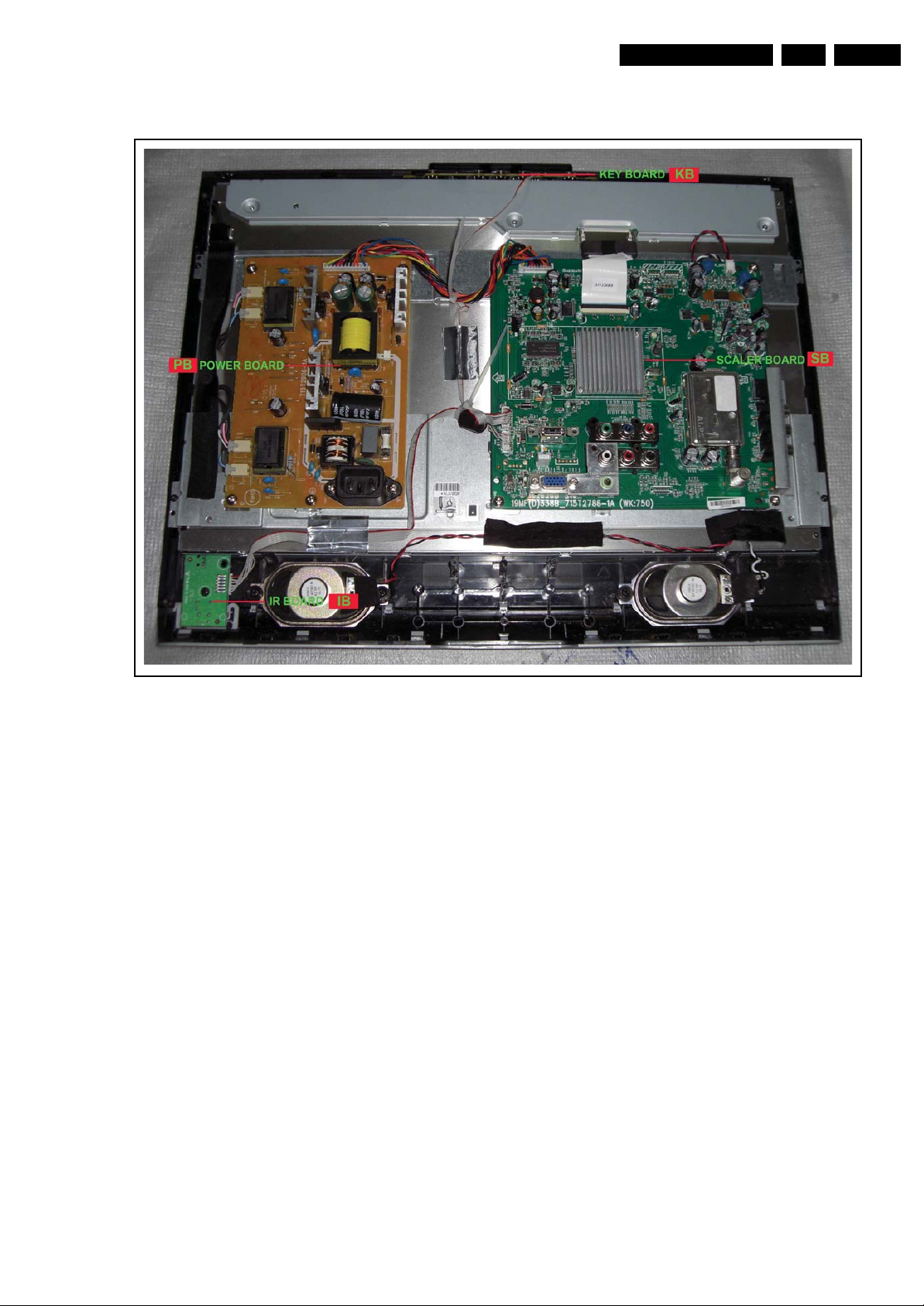
1.3 Chassis Overview
19MF338B
EN 3TPM1.1U LA 1.
Figure 1-3 Chassis Overview
I_17550_059.eps
060308
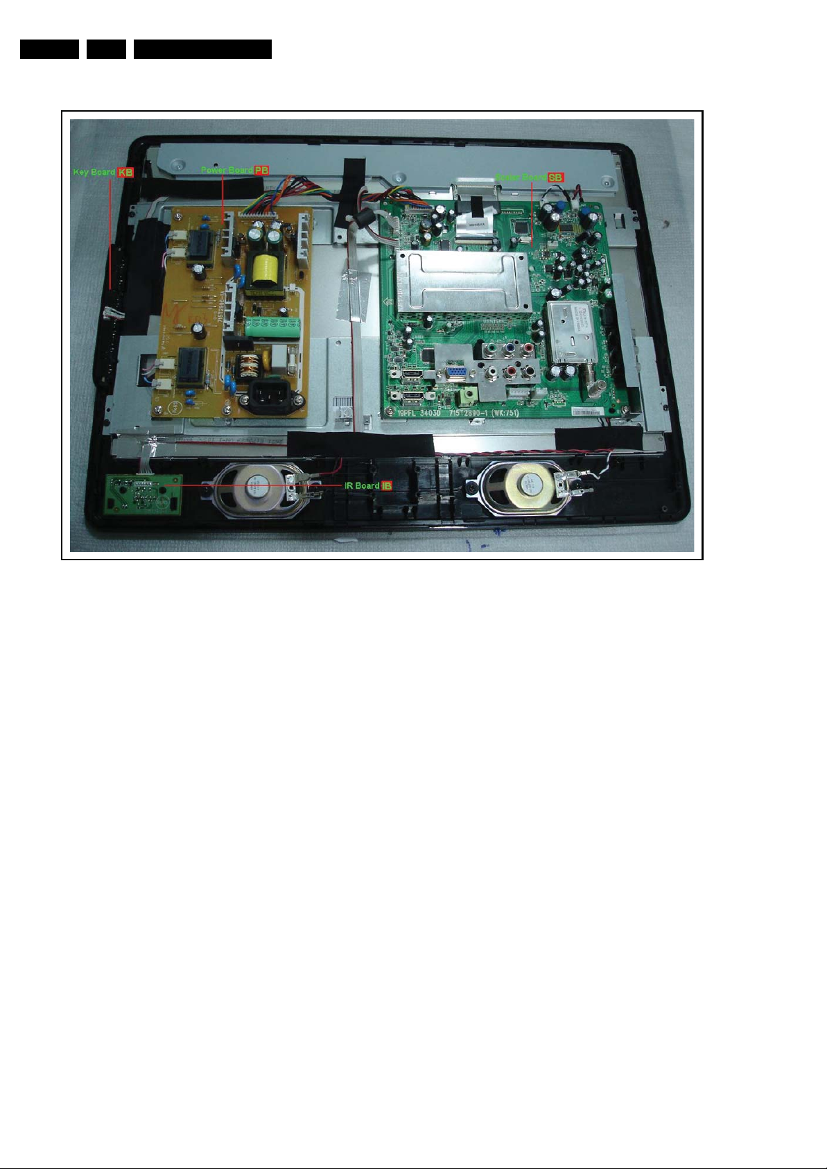
EN 4 TPM1.1U LA1.
19PF3403D
Technical Specifications, Connections, and Chassis Overview
Figure 1-4 Chassis Overview
I_17550_060.eps
060308
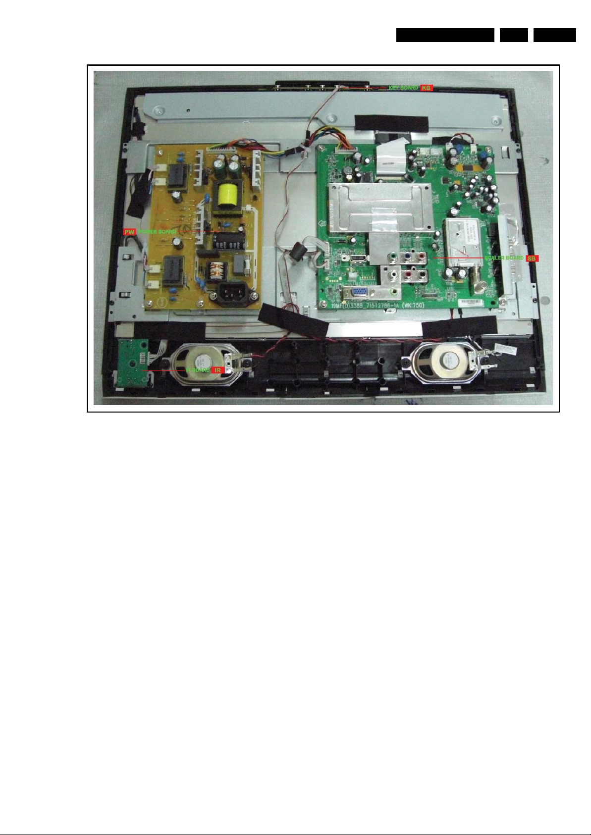
19MD358B
Technical Specifications, Connections, and Chassis Overview
EN 5TPM1.1U LA 1.
Figure 1-5 Chassis Overview
I_17550_061.eps
060308

EN 6 TPM1.1U LA2.
Safety Instructions, Warnings, and Notes
2. Safety Instructions, Warnings, and Notes
Index of this chapter:
2.1 Safety Instructions
2.2 Warnings
2.3 Notes
2.1 Safety Instructions
Safety regulations require the following during a repair:
• Connect the set to the Mains/AC Power via an isolation
transformer (> 800 VA).
• Replace safety components, indicated by the symbol h,
only by components identical to the original ones. Any
other component substitution (other than original type) may
increase risk of fire or electrical shock hazard.
Safety regulations require that after a repair, the set must be
returned in its original condition. Pay in particular attention to
the following points:
• Route the wire trees correctly and fix them with the
mounted cable clamps.
• Check the insulation of the Mains/AC Power lead for
external damage.
• Check the strain relief of the Mains/AC Power cord for
proper function.
• Check the electrical DC resistance between the Mains/AC
Power plug and the secondary side (only for sets that have
a Mains/AC Power isolated power supply):
1. Unplug the Mains/AC Power cord and connect a wire
between the two pins of the Mains/AC Power plug.
2. Set the Mains/AC Power switch to the “on” position
(keep the Mains/AC Power cord unplugged!).
3. Measure the resistance value between the pins of the
Mains/AC Power plug and the metal shielding of the
tuner or the aerial connection on the set. The reading
should be between 4.5 Mohm and 12 Mohm.
4. Switch “off” the set, and remove the wire between the
two pins of the Mains/AC Power plug.
• Check the cabinet for defects, to prevent touching of any
inner parts by the customer.
2.2 Warnings
• All ICs and many other semiconductors are susceptible to
electrostatic discharges (ESD w). Careless handling
during repair can reduce life drastically. Make sure that,
during repair, you are connected with the same potential as
the mass of the set by a wristband with resistance. Keep
components and tools also at this same potential.
• Be careful during measurements in the high voltage
section.
• Never replace modules or other components while the unit
is switched “on”.
• When you align the set, use plastic rather than metal tools.
This will prevent any short circuits and the danger of a
circuit becoming unstable.
2.3 Notes
2.3.1 General
• Measure the voltages and waveforms with regard to the
chassis (= tuner) ground (H), or hot ground (I), depending
on the tested area of circuitry. The voltages and waveforms
shown in the diagrams are indicative. Measure them in the
Service Default Mode (see chapter 5) with a color bar
signal and stereo sound (L: 3 kHz, R: 1 kHz unless stated
otherwise) and picture carrier at 475.25 MHz for PAL, or
61.25 MHz for NTSC (channel 3).
• Where necessary, measure the waveforms and voltages
with (D) and without (E) aerial signal. Measure the
voltages in the power supply section both in normal
operation (G) and in stand-by (F). These values are
indicated by means of the appropriate symbols.
• Manufactured under license from Dolby Laboratories.
“Dolby”, “Pro Logic” and the “double-D symbol”, are
trademarks of Dolby Laboratories.
2.3.2 Schematic Notes
• All resistor values are in ohms, and the value multiplier is
often used to indicate the decimal point location (e.g. 2K2
indicates 2.2 kohm).
• Resistor values with no multiplier may be indicated with
either an “E” or an “R” (e.g. 220E or 220R indicates 220
ohm).
• All capacitor values are given in micro-farads (μ= × 10
nano-farads (n= × 10
• Capacitor values may also use the value multiplier as the
decimal point indication (e.g. 2p2 indicates 2.2 pF).
• An “asterisk” (*) indicates component usage varies. Refer
to the diversity tables for the correct values.
• The correct component values are listed in the Spare Parts
List. Therefore, always check this list when there is any
doubt.
2.3.3 BGA (Ball Grid Array) ICs
Introduction
For more information on how to handle BGA devices, visit this
URL: www.atyourservice.ce.philips.com (needs subscription,
not available for all regions). After login, select “Magazine”,
then go to “Repair downloads”. Here you will find Information
on how to deal with BGA-ICs.
BGA Temperature Profiles
For BGA-ICs, you must use the correct temperature-profile,
which is coupled to the 12NC. For an overview of these profiles,
visit the website www.atyourservice.ce.philips.com (needs
subscription, but is not available for all regions)
You will find this and more technical information within the
“Magazine”, chapter “Repair downloads”.
For additional questions please contact your local repair help
desk.
2.3.4 Lead-free Soldering
Due to lead-free technology some rules have to be respected
by the workshop during a repair:
• Use only lead-free soldering tin Philips SAC305 with order
code 0622 149 00106. If lead-free solder paste is required,
please contact the manufacturer of your soldering
equipment. In general, use of solder paste within
workshops should be avoided because paste is not easy to
store and to handle.
• Use only adequate solder tools applicable for lead-free
soldering tin. The solder tool must be able:
– To reach a solder-tip temperature of at least 400°C.
– To stabilize the adjusted temperature at the solder-tip.
– To exchange solder-tips for different applications.
• Adjust your solder tool so that a temperature of around
360°C - 380°C is reached and stabilized at the solder joint.
Heating time of the solder-joint should not exceed ~ 4 sec.
Avoid temperatures above 400°C, otherwise wear-out of
tips will increase drastically and flux-fluid will be destroyed.
To avoid wear-out of tips, switch “off” unused equipment or
reduce heat.
• Mix of lead-free soldering tin/parts with leaded soldering
tin/parts is possible but PHILIPS recommends strongly to
-9
), or pico-farads (p= × 10
-12
-6
),
).

avoid mixed regimes. If this cannot be avoided, carefully
clear the solder-joint from old tin and re-solder with new tin.
2.3.5 Alternative BOM identification
The third digit in the serial number (example:
AG2B0335000001) indicates the number of the alternative
B.O.M. (Bill Of Materials) that has been used for producing the
specific TV set. In general, it is possible that the same TV
model on the market is produced with e.g. two different types
of displays, coming from two different suppliers. This will then
result in sets which have the same CTN (Commercial Type
Number; e.g. 28PW9515/12) but which have a different B.O.M.
number.
By looking at the third digit of the serial number, one can
identify which B.O.M. is used for the TV set he is working with.
If the third digit of the serial number contains the number “1”
(example: AG1B033500001), then the TV set has been
manufactured according to B.O.M. number 1. If the third digit is
a “2” (example: AG2B0335000001), then the set has been
produced according to B.O.M. no. 2. This is important for
ordering the correct spare parts!
For the third digit, the numbers 1...9 and the characters A...Z
can be used, so in total: 9 plus 26= 35 different B.O.M.s can be
indicated by the third digit of the serial number.
Identification: The bottom line of a type plate gives a 14-digit
serial number. Digits 1 and 2 refer to the production center (e.g.
AG is Bruges), digit 3 refers to the B.O.M. code, digit 4 refers
to the Service version change code, digits 5 and 6 refer to the
production year, and digits 7 and 8 refer to production week (in
example below it is 2006 week 17). The 6 last digits contain the
serial number.
Directions for Use
MODEL :
PROD.NO:
32PF9968/10
AG 1A0617 000001
220-240V 50/60Hz
VHF+S+H+UHF
S
Figure 2-1 Serial number (example)
2.3.6 Board Level Repair (BLR) or Component Level Repair
(CLR)
If a board is defective, consult your repair procedure to decide
if the board has to be exchanged or if it should be repaired on
component level.
If your repair procedure says the board should be exchanged
completely, do not solder on the defective board. Otherwise, it
cannot be returned to the O.E.M. supplier for back charging!
2.3.7 Practical Service Precautions
• It makes sense to avoid exposure to electrical shock.
While some sources are expected to have a possible
dangerous impact, others of quite high potential are of
limited current and are sometimes held in less regard.
• Always respect voltages. While some may not be
dangerous in themselves, they can cause unexpected
reactions that are best avoided. Before reaching into a
powered TV set, it is best to test the high voltage insulation.
It is easy to do, and is a good service precaution.
EN 7TPM1.1U LA 3.
MADE IN BELGIUM
~
128W
BJ3.0E LA
E_06532_024.eps
130606
3. Directions for Use
You can download this information from the following websites:
http://www.philips.com/support
http://www.p4c.philips.com
EN 8 TPM1.1U LA4.
Mechanical Instructions
4. Mechanical Instructions
Index of this chapter:
1. Cable Dressing
2. Service Positions
3. Assy/Panel Removal
4. Re-assembly
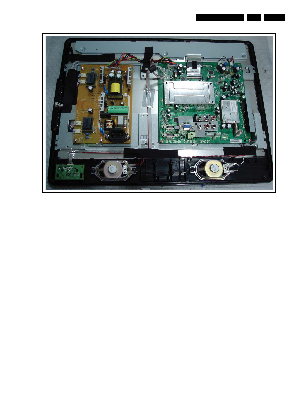
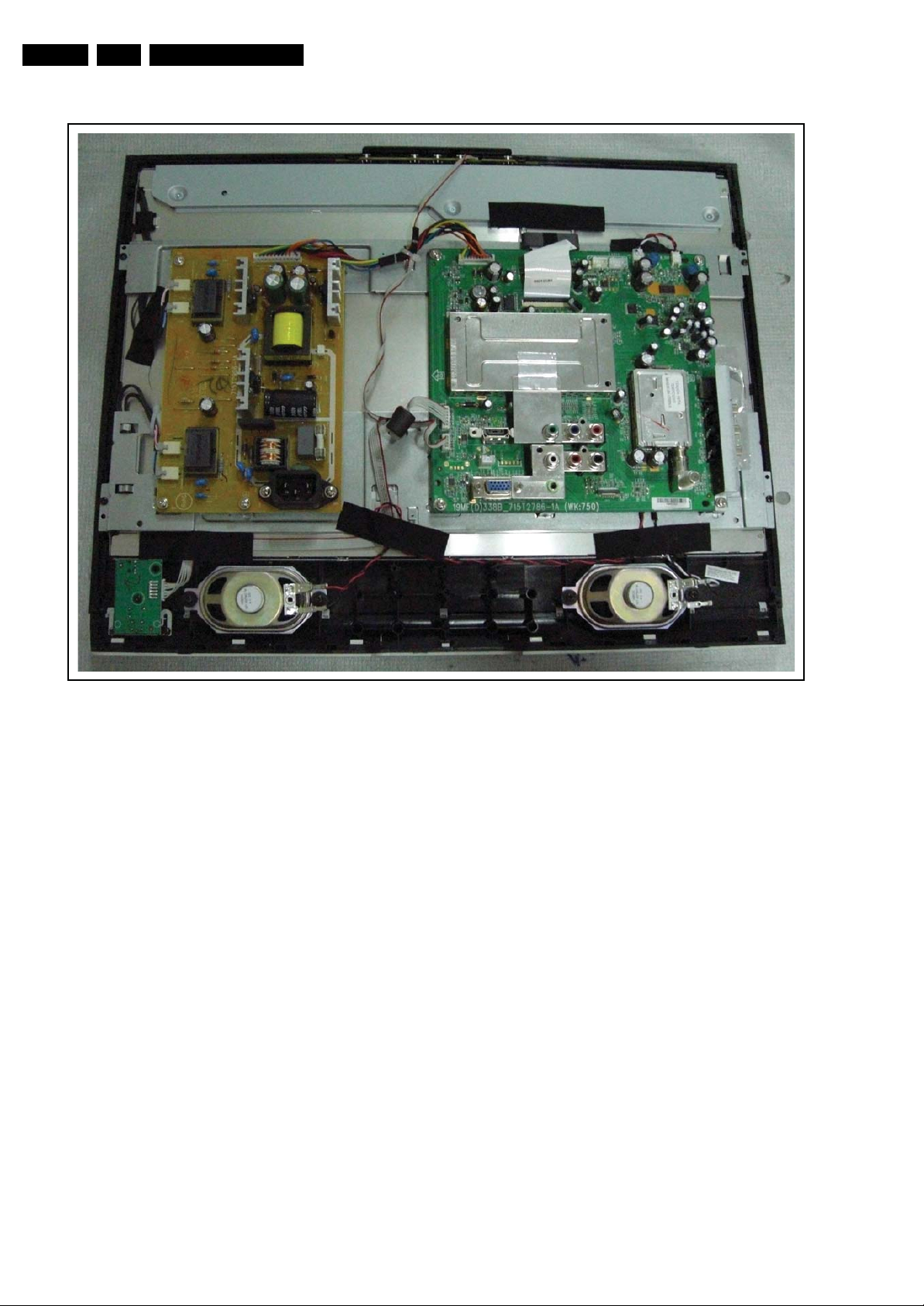
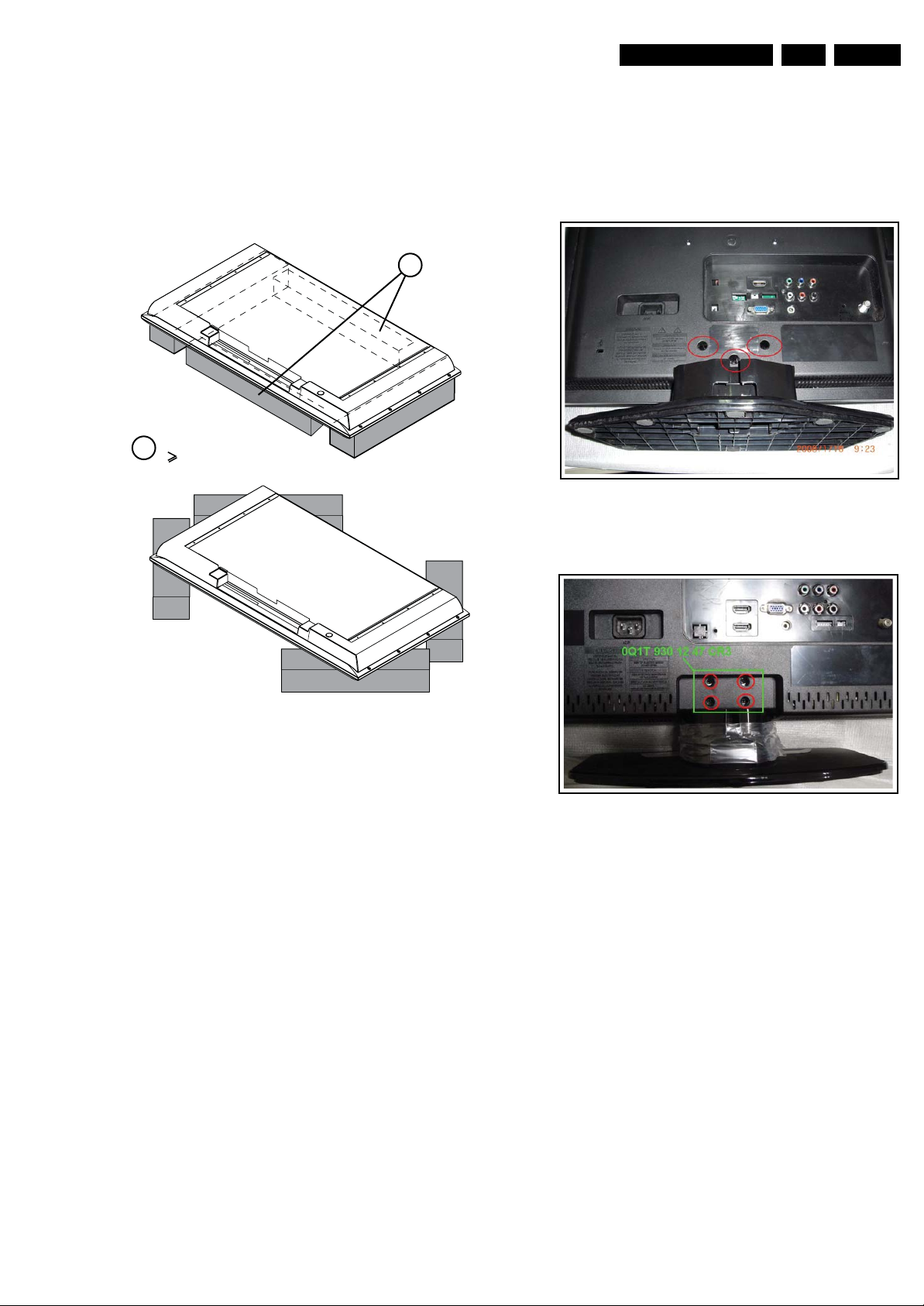
4.1 Cable Dressing
Notes:
• Figures below can deviate slightly from the actual situation,
due to the different set executions.
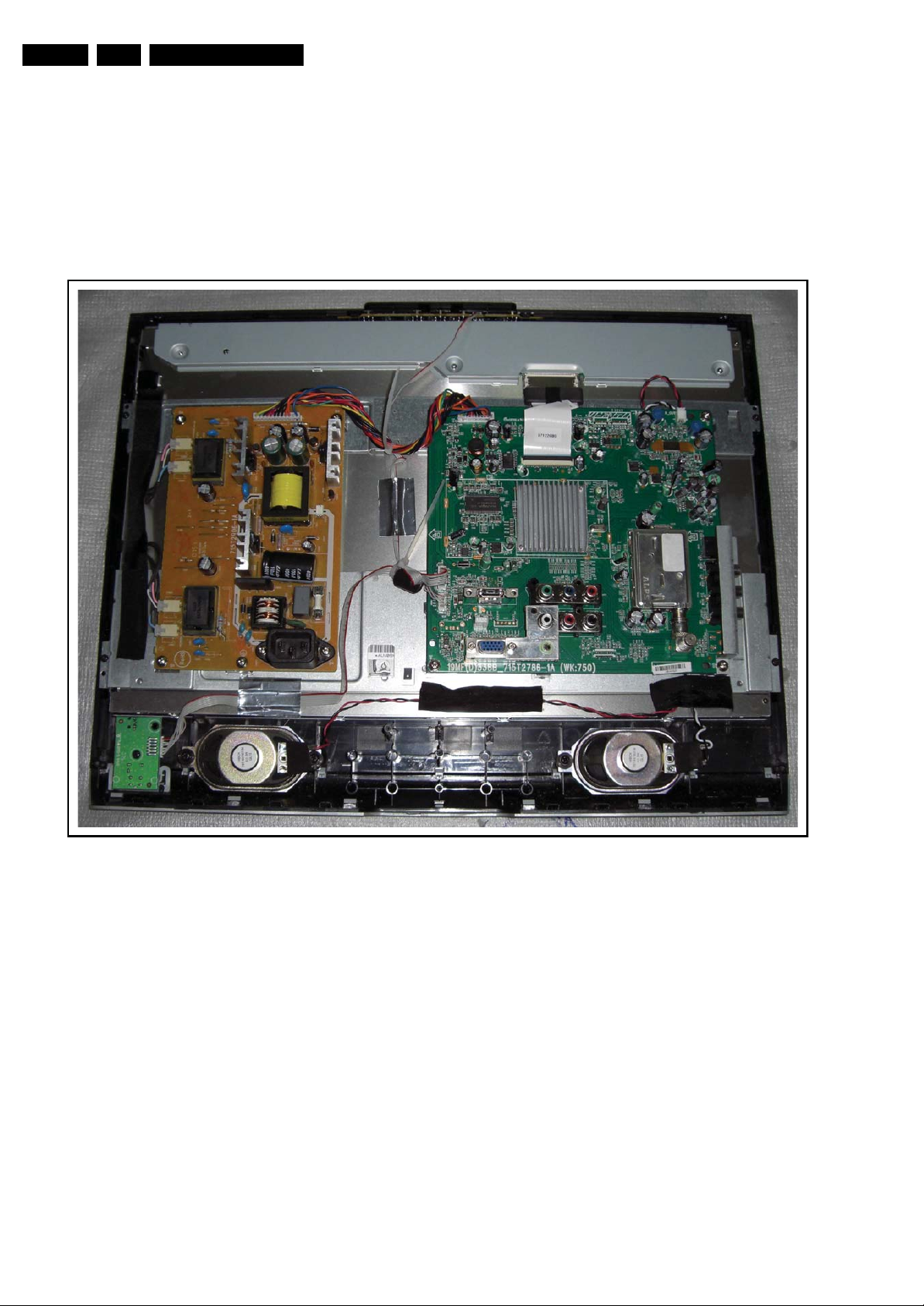
• Follow the disassembly instructions in the described order.
Figure 4-1 Cable dressing(19MF338B)
I_17550_062.eps
060308
Mechanical Instructions
EN 9TPM1.1U LA 4.
Figure 4-2 Cable dressing(19PFL3403D)
I_17550_063.eps
060308
EN 10 TPM1.1U LA4.
Mechanical Instructions
Figure 4-3 Cable dressing (19MD358B)
I_17550_064.eps
060308
Mechanical Instructions
EN 11TPM1.1U LA 4.
4.2 Service Positions
For easy servicing of this set, there are a few possibilities
created:
• The buffers from the packaging (see figure "Rear cover").
• Foam bars (created for Service).
4.2.1 Foam Bars
Required for sets
1
42"
4.3 Assy/Panel Removal
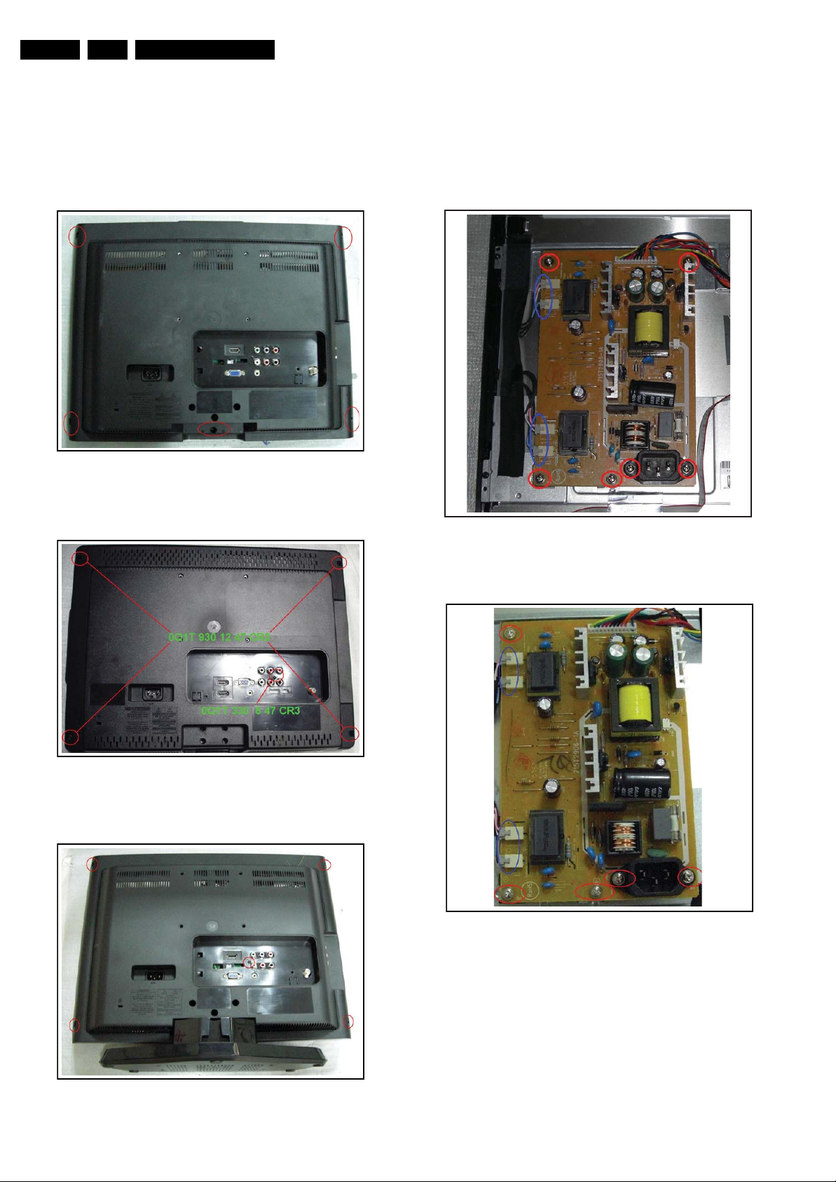
4.3.1 Stand/Base
Remove the screws remarked in red to remove the stand or
base.
19MF338B
1
I_17550_065.eps
060308
Figure 4-5 Remove base
E_06532_018.eps
171106
Figure 4-4 Foam bars
The foam bars (order code 3122 785 90580 for two pieces) can
be used for all types and sizes of Flat TVs. See figure “Foam
bars” for details. Sets with a display of 42” and larger, require
four foam bars [1]. Ensure that the foam bars are always
supporting the cabinet and never only the display.
Caution: Failure to follow these guidelines can seriously
damage the display!
By laying the TV face down on the (ESD protective) foam bars,
a stable situation is created to perform measurements and
alignments. By placing a mirror under the TV, you can monitor
the screen.
19PFL3403D
Figure 4-6 Remove base
I_17550_066.eps
060308
EN 12 TPM1.1U LA4.
Mechanical Instructions
4.3.2 Rear Cover
1. Remove the screws remarked in red, which secure the rear
cover. The screws are located at the top, bottom, left and
right sides.
2. Lift the rear cover from the cabinet. Make sure that wires
and flat foils are not damaged during cover removal.
19MF338B
I_17550_067.eps
060308
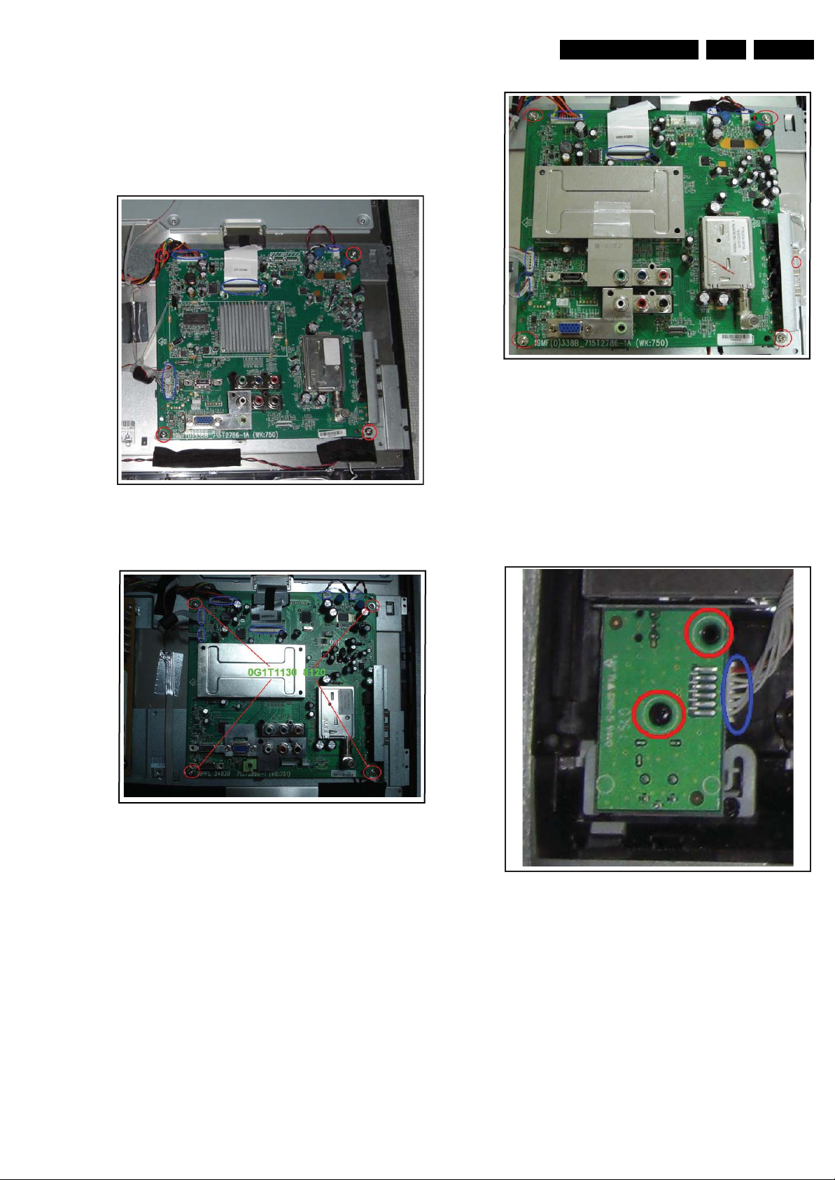
4.3.3 Power Board
1. Refer to next figure
2. Unplug connector remarked in blue.
3. Release screws(0G1T 1130 8120 and 0G1T 1130
10120)remarked in red and remove the board.
When defective,replace the whole unit
19MF338B&19PFL3403D
Figure 4-7 Remove rear cover
19PFL3403D
Figure 4-8 Remove rear cover
19MD358B
I_17550_068.eps
060308
19MD358B
Figure 4-10 Power Board
I_17550_005.eps
120208
Figure 4-9 Remove rear cover
I_17550_080.eps
070308
Figure 4-11 Power Board
I_17550_069.eps
060308
Mechanical Instructions
EN 13TPM1.1U LA 4.
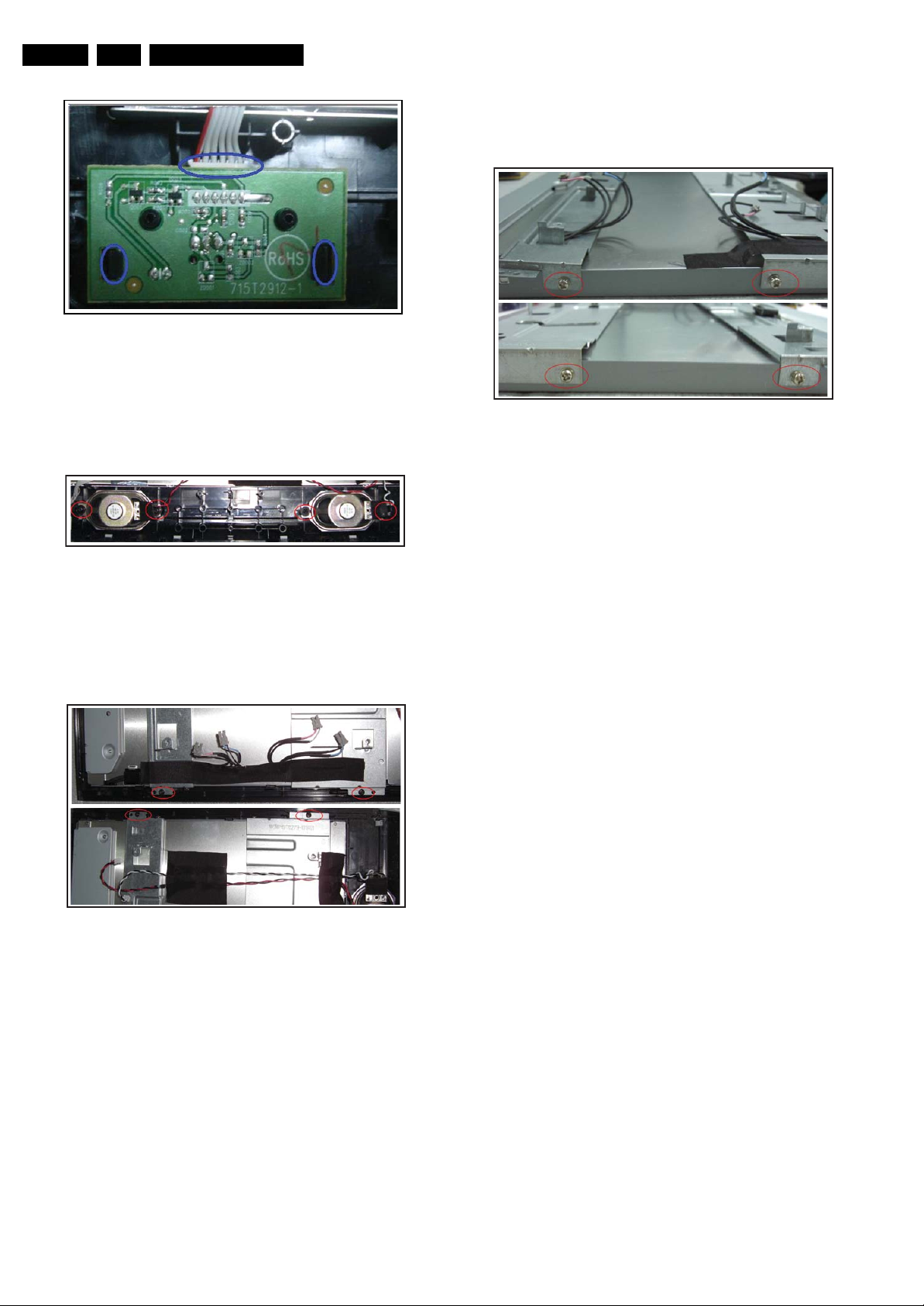
4.3.4 Main Board
1. Refer to next figure
2. Unplug connector remarked in blue.
3. Replease screws remarked in red and remove the board.
When defective, replace the whole unit.
19MF338B
Figure 4-12 Main Board
I_17550_006.eps
120208
19MD358B
Figure 4-14 Main Board
4.3.5 IR Board
1. Refer to next figure
2. Unplug the connector remarked in blue.
3. Remove the screws remarked in red and remove the IR
board.
When defective,replace the whole unit.
I_17550_073.eps
060308
19PFL3403D
Figure 4-13 Main Board
I_17550_072.eps
060308
19MF338B & 19MD358B
Figure 4-15 IR Board
I_17550_007.eps
120208
EN 14 TPM1.1U LA4.
Mechanical Instructions
19PFL3403D
Figure 4-16 IR Board
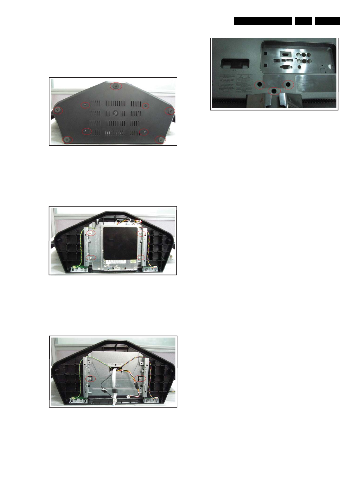
4.3.6 Speakers
1. Refer to next figure.
2. Remove the screws remarked in red.
I_17550_070.eps
060308
4.3.8 Bracket
1. Refer to next two figures.
2. Remove the screws remarked in red.
Figure 4-19 Bracket
I_17550_009.eps
120208
Figure 4-17 Speakers
4.3.7 Bezel
1. Refer to next two figures.
2. Remove the screws remarked in red.
Figure 4-18 Bezel
I_17550_055.eps
060308
I_17550_008.eps
060308
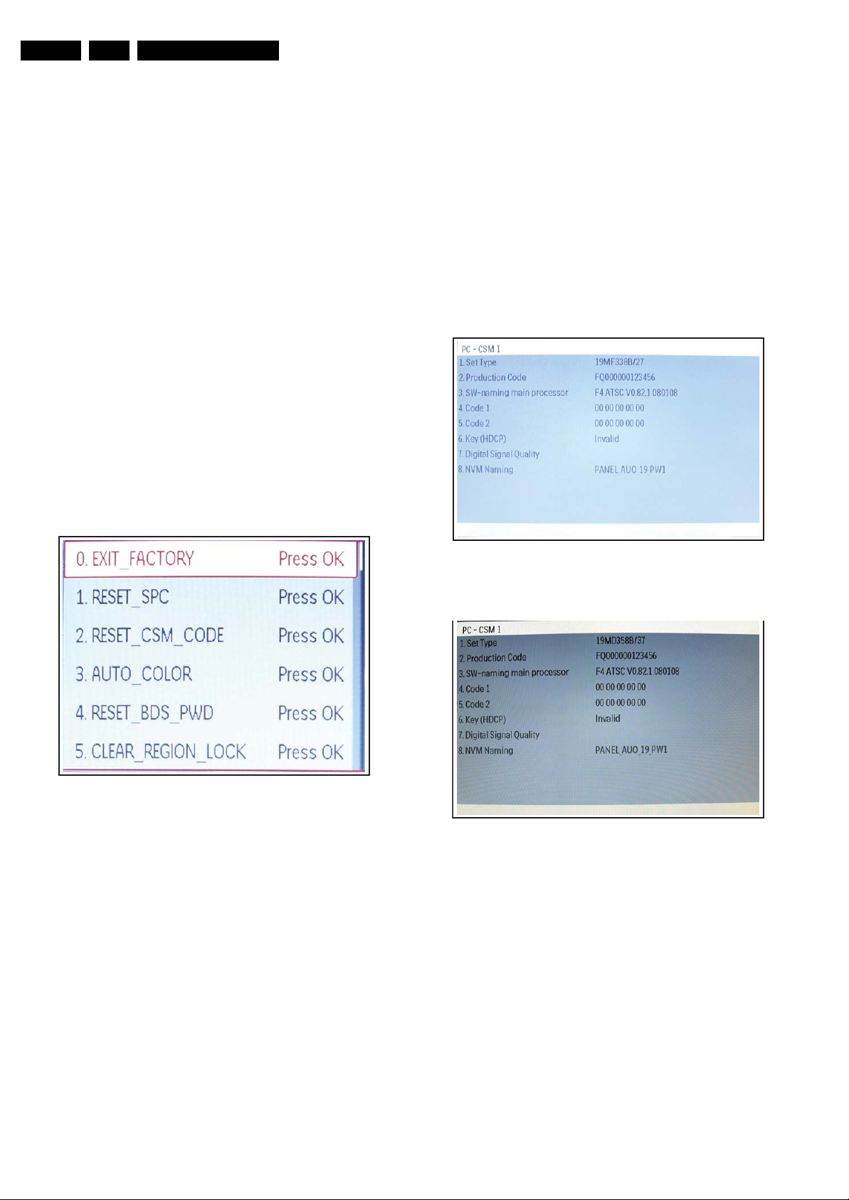
4.4 19MD358B DVD Base Removal
4.4.1 Cover_BOTTOM_DVD_Base
Remove the screws remarked in red to remove the
Cover_BOTTOM_DVD_Base.
Mechanical Instructions
Figure 4-23 Rear Cover(19MD358B)
EN 15TPM1.1U LA 4.
I_17550_077.eps
060308
Figure 4-20 Cover_BOTTOM_DVD_Base
4.4.2 QSI_SLIM_DVD_PLAYER
Remove the screws remarked in red to remove the
QSI_SLIM_DVD_Player.
Figure 4-21 QSI_SLIM_DVD_PLAYER
4.4.3 FRAME_DVD Base
I_17550_074.eps
060308
I_17550_075.eps
060308
4.5 Set Re-assembly
To re-assemble the whole set, execute all processes in reverse
order.
Notes:
• While re-assembling, make sure that all cables are placed
and connected in their original position. See figure "Cable
dressing".
Remove the screws remarked in red to remove the
FRAME_DVD Base.
Figure 4-22 FRAME_DVD Base
4.4.4 Rear Cover
Remove the screws remarked in red to remove the rear cover.
I_17550_076.eps
060308
EN 16 TPM1.1U LA5.
Service Modes, Error Codes, and Fault Finding
5. Service Modes, Error Codes, and Fault Finding
Index of this chapter:
5.1 Test Points
5.2 Service Mode
5.3 Service Tools
5.1 Test Points
This chassis is NOT equipped with test points in the service
printing. These test points are NOTspecifically mentioned in
the service manual
5.2 Service Mode
5.2.1 Factory Mode
How to Enter
To enter the Factory mode,use one of the following methods:
• To hold”Volume+” and “Volume-” buttons,then power on
while there is video signal in.Monitor will enter factory
mode automatically once power is off.
• Press remote control code”062596” ,then press menu key.
Caution: This fuctions are avaible for development and
service personnal only,not for end customers.
After entering factory mode, the following screen is visible, the
values can be adjusted according to the requested.
Also new in this chassis:when you activate CSM and there is a
USB stick connected to the TV,the software will dump the
complete CSM content to the USB stick,The file(CSM.txt) will
be saved in the root of your USB stick.This info can be handy if
you donot have picture.
How to Activate CSM
Key in the code”123654” via the standard RC transmitter.
How to Navigate
By mean of the “CURSOR-DOWN/UP” knob on the RCtransmitter on the screen.
Contents of CSM
Figure 5-1 Factory mode menu
How to EXIT
Choose ‘EXIT”,then press “OK” botton on remote control.
5.2.2 Customer Service Mode(CSM)
Purpose
When a customer is having problems with his TV-set,he can
call his dealer or the Customer Helpdesk.The service
technician can then ask the customer to actrivate the CSM in
order to identify the status of the set.Now,the service technician
can judge the erverity of the complain.In many cases,he can
advise the customer how to solve the problem or he can decide
if it is necessary to visit the customer.The mode are not
possible.
I_17550_010.eps
060208
Figure 5-2 CSM Menu(19MF338B)
Figure 5-3 CSM Menu(19PFL3403D)
I_17550_011.eps
060308
I_17550_079.eps
060308
When in this chassis,CSM is activated,a clour bar test pattern
will be visible for 5 seconds.This test pattern is generated by
the pacific 3.So if you see this test pattern you can determine
that the back end video chain(pacific3,LVDS and display) is
working.
Service Modes, Error Codes, and Fault Finding
TO
UART SERVICE
CONNECTOR
TO TV
TO
I2C SERVICE
CONNECTOR
TO
UART SERVICE
CONNECTOR
EN 17TPM1.1U LA 5.
I_17550_079.eps
060308
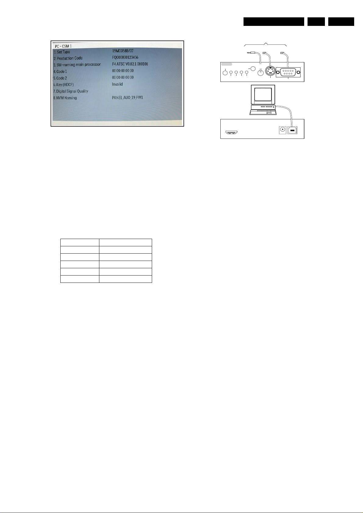
Figure 5-4 CSM Menu(19MD358)
Menu Explanation
1. Set Type. Type number and region.
2. Production code. Product serial no.
3. SW naming main-processor. Software cluster and version
is displayed.
4. Code 1. Error buffer contents.
5. Code 2. Error buffer contents.
(for the data of code 1/2, please refer to the table below)
6. Key (HDCP): Indicates if the keys are valid.
7. Digital Signal Quantity
8. NVM-naming: Indicates the used LCD panel type and
region (NVM content and main SW depend on the used
LCD panel).
Error Code Error Code Type
00 OK
01 DDR may fail
02 EEPROM may fail
03 TUNER may fail
04 MT5380ACU may fail
ComPair II
RC in
Optional
Switch
Power ModeLink/
HDMI
I
Activity
2
C only
RC out
Multi
function
2
I
C
PC
ComPair II Developed by Philips Brugge
Optional power
5V DC
RS232 /UART
E_06532_036.eps
150208
Figure 5-5 ComPair II interface connection
Caution: It is compulsory to connect the TV to the PC as
shown in the picture above (with the ComPair interface in
between), as the ComPair interface acts as a level shifter. If
one connects the TV directly to the PC (via UART), ICs will be
blown!
How to Order
ComPair II order codes:
• ComPair II interface: 3122 785 91020.
• For SW see Philips service website.
• ComPair UART interface cable: 3122 785 90630.
Note: If you encounter any problems, contact your local
support desk.
5.3.2 LVDS Tool
Support of the LVDS Tool has been discontinued.
How to exit
Press”MENU” on the RC-transmitter.
5.3 Service Tools
5.3.1 ComPair
Introduction
ComPair (Computer Aided Repair) is a Service tool for Philips
Consumer Electronics products. and offers the following:
1. ComPair helps you to quickly get an understanding on how
to repair the chassis in a short and effective way.
2. ComPair allows very detailed diagnostics and is therefore
capable of accurately indicating problem areas. You do not
have to know anything about I
yourself, because ComPair takes care of this.
3. ComPair speeds up the repair time since it can
automatically communicate with the chassis (when the uP
is working) and all repair information is directly available.
4. ComPair features TV software upgrade possibilities.
Specifications
ComPair consists of a Windows based fault finding program
and an interface box between PC and the (defective) product.
The (new) ComPair II interface box is connected to the PC via
an USB cable. For the TV chassis, the ComPair interface box
and the TV communicate via a bi-directional cable via the
service connector(s).
2
C or UART commands
How to Connect
This is described in the ComPair chassis fault finding database.

EN 18 TPM1.1U LA5.
Personal Notes:
Service Modes, Error Codes, and Fault Finding
E_06532_012.eps
131004
Block Diagrams, Test Point Overview, and Waveforms
p
A
A
6. Block Diagrams, Test Point Overview, and Waveforms
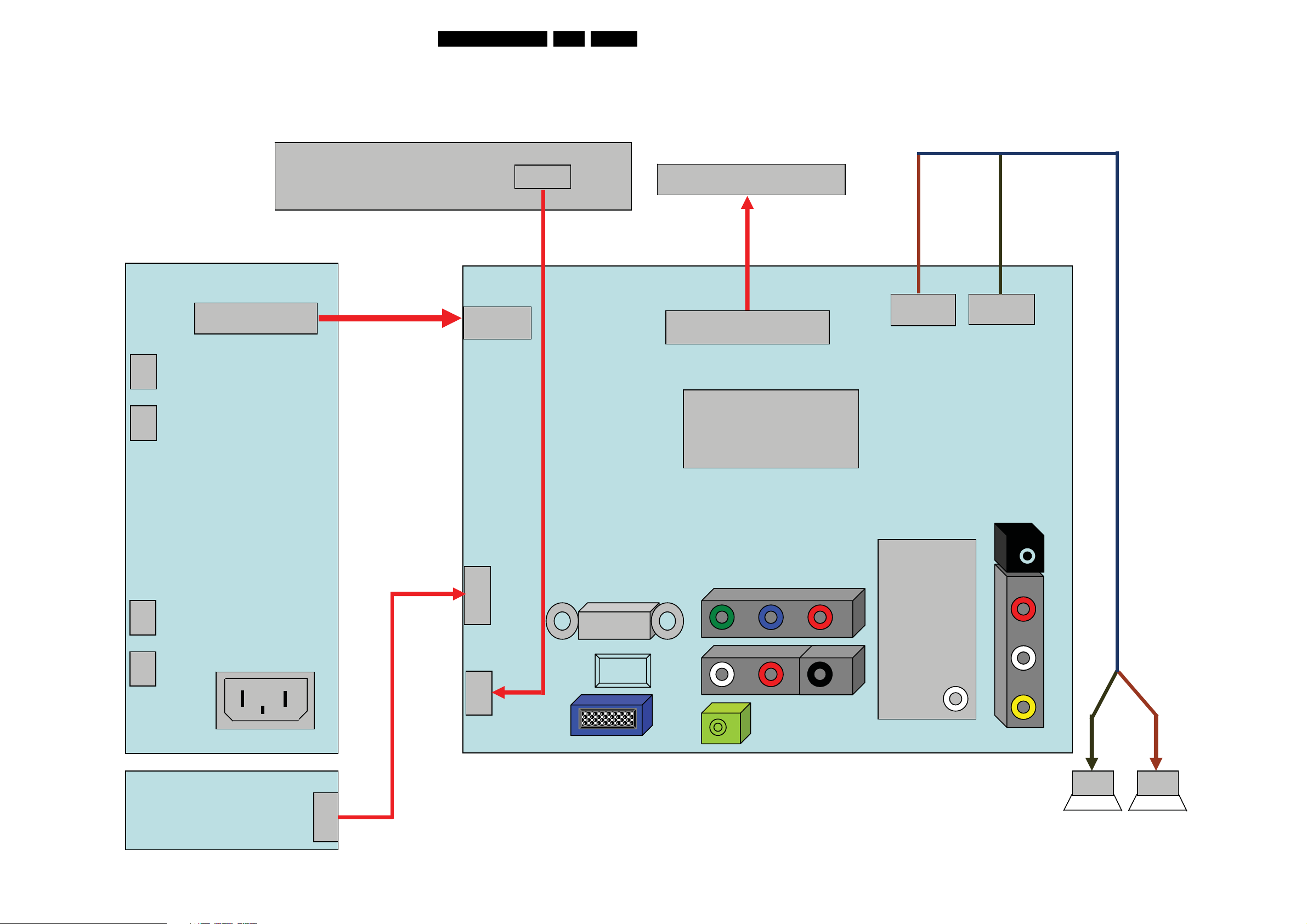
Wiring Diagram 19MF338B
WIRING DIAGRAM
19TPM1.1U LA 6.
1
CN825
CN824
11 Pin
CN902
12
Key Board
95T801412F901
HARNESS 75120
1
11 pin
CN101
CN016
3Pin
1
11
3
95T8014 4X901
HARNESS TE0003
95T8013 2X901
HARNESS TE0004
HARNESS TE0005
95T8013 2X902
Panel
89T179E30C919
FFC Cable
2
1
30
2
1
2pin 2
30 pin
CN602
CN601
CN701
MT5380ACU
LQFP256
U400
1
in
Power Board
CN823
CN821
CN901
C IN
Scaler Board
Head Phone
1
6Pin
YPbPr
CN301
95T8014 6X901
HARNESS TE0001
6
HDMI
udio R/L in SPDIF Out
R/F
Side AV
1
4Pin
CN302
PC Audio in
4
PC D-SUB
11
IR Board
CN001
Speaker R/L
I_17550_081.eps
6
070308
Block Diagrams, Test Point Overview, and Waveforms
A
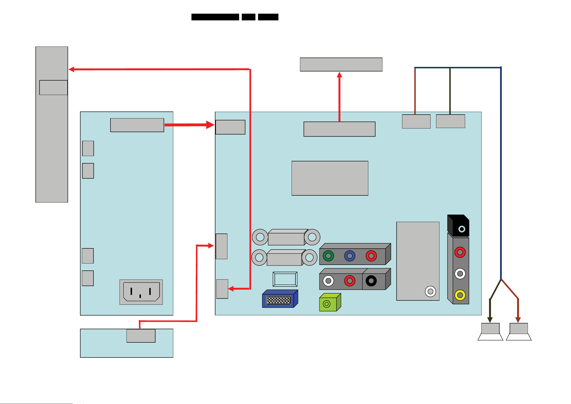
Wiring Diagram 19PFL3403D
20TPM1.1U LA 6.
WIRING DIAGR
Key
M
95T8014 4F902
Panel
Board
4
4 Pin
1
CN016
1
12 Pin
CN902
CN853
CN851
HARNESS 75129
12
95T801412X901
HARNESS 75120
1
11 pin
CN101
11
30 Pin
30
CN701
MT5380ACU
LQFP256
89T179E30C920
FFC Cable
1
95T8013 2X901
HARNESS TE0004
2 Pin 2Pin
CN602
95T8013 2X902
CN601
HARNESS TE0005
1212
Power Board
CN833
CN831
CN901
1
AC IN
U400
Main Board
Head Phone
1
6Pin
HDMI 1
YPbPr
CN301
95T8014 6F902
HARNESS 75128
6
HDMI 2
Audio R/L in
SPDIF Out
R/F
Side AV
1
4Pin
CN302
PC Audio in
4
PC D-SUB
6
IR Board
6 Pin
CN001
Speaker R/L
I_17550_082.eps
070308
Block Diagrams, Test Point Overview, and Waveforms
p
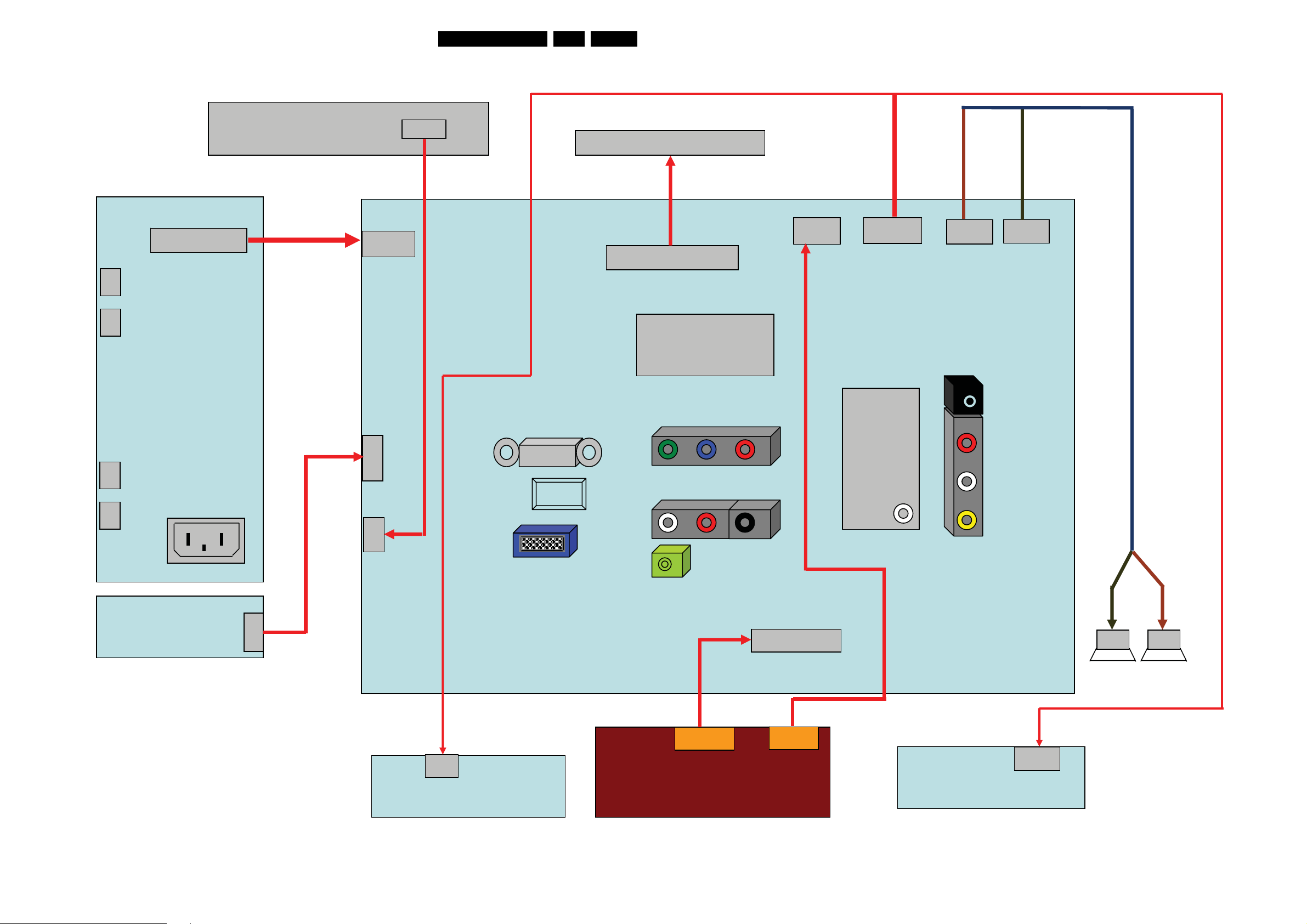
Wiring Diagram 19MD358B
WIRING DIAGRAM
Key Board
CN016
3Pin
1
21TPM1.1U LA 6.
95T8014 4F901
95T8013 2X901
HARNESS TE0004
3
95T8014 5F901
HARNESS 75126
Panel
HARNESS TE0005
95T8013 2X902
HARNESS 4P-3P
1
11 Pin
CN902
CN853
CN851
Power Board
CN833
CN831
AC IN
12
095T801412X90
HARNESS TE0002
HARNESS TE0001
95T8014 6X901
1
11 pin
CN101
1
6Pin
6
1
4Pin
11
CN301
CN302
95T8014 4X901
HARNESS TE0003
HDMI
ISP
89T179E30C919
FFC CABLE 30P
30
CN701
Audio R/L in
in
301
MT5380ACU
LQFP256
U400
Scaler Board
YPbPr
SPDIF Out
1
4
6
4pin 6pin
CN150
CN303
R/F
1
2
2
1
2pin
CN602
CN601
1
2pin
Head Phone
Side AV
CN901
IR Board
CN001
4
PC D-SUB
PC Audio in
HARNESS 75125
95T8014 4F903
161
16
89T176E 16912
1
FFC CABLE 16P
16 Pin
CN750
Speaker R/L
4
2pin
1
2
CN060
DVD Key Board
16 pin
1
DVD MODULE
16
4 pin
1
4
4pin
DVD LED Board
CN080
1
I_17550_083.eps
070308
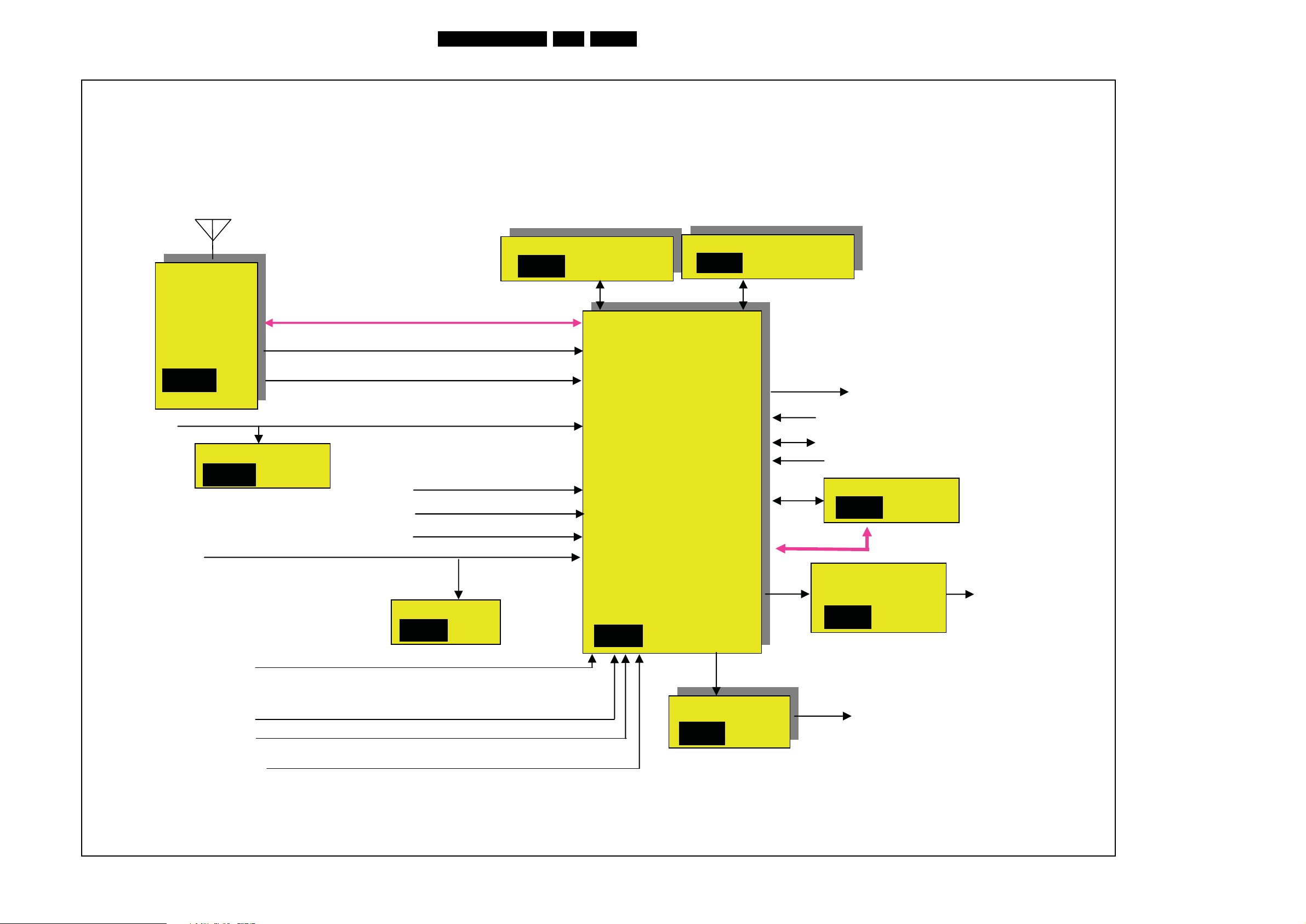
Block Diagrams, Test Point Overview, and Waveforms
Block Diagram Power Supply
POWER SUPPLY
22TPM1.1U LA 6.
+5V / LC
filter to
+5Vc
+12V
+3V3SB LD1117S33
+5Vc/60mA
DV33SB SW_SI3441 / 50mA
RC filter x 1 + LC filter x 3 Tuner
+5V_SW MOS
Switch SI5441 1.5A
+5V_TUNER 0.35A Alps 507A
AV33 LD1117S33
DV33 LD1117S33
AV25 700mA D1117ADTR
IR 2mA
5mA for WT6702 (Optional)
50mA for MTK5380
350mA for MT5380
100mA for Flash / EEPROM
AV12 LD1117DTTR for MT5380
+12V
DDRV 2V6 LD1117ADTR 650mA
Panel_Vcc MOS
Switch SI5441
Panel_Vcc for LVDS 5V / 1.2A for 19”
DV11 D-D Buck
L5985
DV11/ 1.2A for MT5380
+12V for iPod 10W Subwoofer & Battery charge 1.3A
LP2996 1V8 to DDR1 x1
TDA8933 Audio AMP+12V for Audio 3Wx2 / 600mA
I_17550_084.eps
170308
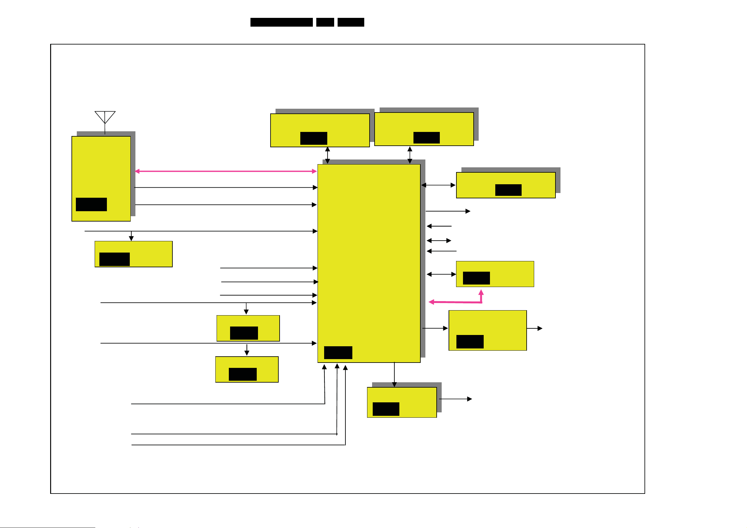
Block Diagrams, Test Point Overview, and Waveforms
Block Diagram Scaler Board 19MF338B & 19MD358B
23TPM1.1U LA 6.
DS
DS
Combo
Tuner
TDQU4-507A
SB-03
PC D-SUB
UXGA 162MHz
( Magnavox )
( Magnavox )
I2C
IFAT +/-
CVBS + 2nd IF
DDC 24C02
SB-08
HD YPbPr
CVBS
Function block of main Board w/ MT5380AACCUU
Function block of main Board w/ MT5380
DDR1 256Mbit x1
SB-04
Serial Flash 4MByte
SB-06
MT5380ACU
.MCU
.DTV receiver
.ATV demodulation
.MPEG/video/audio
decoder
.Scaling
.Video enhancement
LVDS to panel
RC
UART for ISP & Comair & iTV level 1
Keys
M24C16-MN6T
SB-05
HDMI-1
Audio R/L of CVBS
Audio R/L of YPbPr
Audio R/L of PC
Audio R/L of DVD YPbPr
DVD YPbPr
DDC 24C02
SB-07
.3D comb
.LVDS Transmitter
.HDMI 1.3a Receiver
.ADC
SB-05
TDA8933BTW
SB-11
I2C
HP OP AMP
LM4809MA
SB-12
speakers
Headphone
I_17550_085.eps
070308
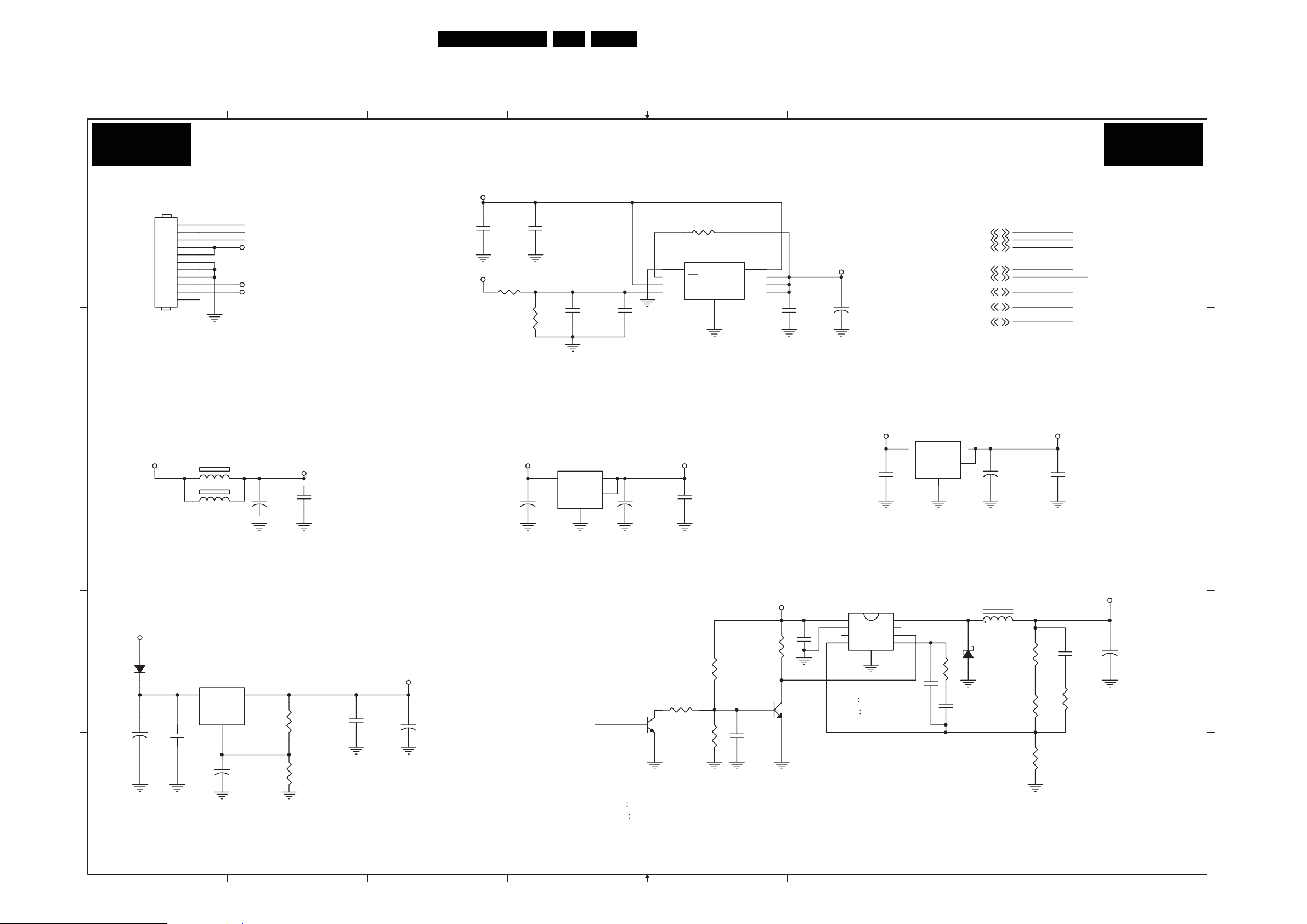
Block Diagrams, Test Point Overview, and Waveforms
Block Diagram Scaler Board 19PFL3403D
24TPM1.1U LA 6.
DS((
DS
Combo
Tuner
TDQU4-507A
SB-03
PC D-SUB
UXGA 162MHz
OTS))
OTS
IFAT +/-
CVBS + 2nd I F
DDC 24C02
SB-08
Function block of main Board w/ MT5380AACCUU
Function block of main Board w/ MT5380
DDR1 256Mbit x1
SB-04
2
I
C
MT5380ACU
.MCU
.DTV receiver
.ATV demodulation
.MPEG/video/audio
decoder
HD YPbPr
CVBS
.Scaling
.Video enhancement
WT61P7-RN440WT
ECE MCU
SB-14
Serial Flash 32 MByte
SB-06
LVDS to panel
RC
UART for ISP
Keys
M24C16-MN6T
SB-05
HDMI-1
HDMI-2
Audio R/L of CVBS
Audio R/L of YPbPr
Audio R/L of PC
DVD YPbPr
DDC 24C02
SB-07
DDC 24C02
SB-07
.2D comb
.LVDS Transmitter
.HDMI 1.3a Receiver
.ADC
SB-05
TDA8933BTW
SB-11
2
C
I
HP OP AMP
LM4809MA
SB-12
Headphone
speakers
I_17550_086.eps
170308
Circuit Diagrams and PWB Layouts
25TPM1.1U LA 7.
7. Circuit Diagrams and PWB Layouts
Scaler Board: Power Part 1
1
2
3
4
5
6
7
8
SCALAR BOARD: POWER 1
SB01 SB01
63391 11P 2.0MM
11
10
BRIGHT_ADJ
CN101
9
8
7
6
5
4
3
2
1
A A
PID
INVERTER_ON_OFF
+5V
+12V
+12V
VTT
C103
4.7UF 10V
R102
DDRV
NC/75R 1/10W 1%
R103
NC/75R 1/10W 1%
C104
100N 16V
MEM_VREF
C105
100N 16V
C106
1U 10V
R101
4K7 1/10W 5%
U101
1
GND
2
SD
3
VSENSE
4
VREF VDDQ
PVIN
AVI N
HS
9
8
VTT
7
6
5
LP2996MRX
C107
100N 16V
DDRV
+
C108
100uF 16V
{5,7}
INVERTER_ON_OFF
{14}
MEM_VREF{5}
VTT{5}
DDRV
BRIGHT_ADJ{14}
OPWRSB{3,6}
PID{14}
OPCTRL5{6,7}
MEM_VREF
VTT
DDRV
BRIGHT_ADJ
INVERTER_ON_OFF
OPWRSB
PID
OPCTRL5
VTT FOR DDR TERMINATOR
B
+5V
C C
FB101
12
BEAD
1
FB102 BEAD
+
2
+5Vc
C101
1000uF 10V
C102
100N 16V
C114
100uF 16V
+5V_SW
MEM_VREF FOR DDR AND MT5381 VREF
U103 LD1117S33
3
VI VO
+
2
4
TH1
GND
1
C115
+
100uF 16V
A.I
DV33
C113
100N 16V
+5Vc
3 2
C116
22U 10V
U104 LD1117S33
VI VO
TH1
GND
1
+3V3SB
4
C117
+
100uF 16V
C121
100N 16V
CN101 A1 C101 C2
C102 C2 C103 A3
C104 A4 C105 A4
C106 A4 C107 A5
C108 A6 C109 D6
C110 D8 C111 D6
C112 D7 C113 C5
C114 C4 C115 C4
C116 C6 C117 C7
C118 D2 C119 D3
C120 D1 C121 C7
C122 D1 C123 E1
C124 D7 C125 D5
D101 D1 D102 D7
FB101 C1 FB102 C1
L101 D7 Q101 D4
Q102 D5 R101 A5
R102 A3 R103 A4
R104 D5 R105 D7
R107 D7 R108 D7
R109 E7 R110 D2
R111 E2 R112 D7
R113 D5 R114 D5
R115 D5 U101 A5
U102 D6 U103 C4
U104 B6 U105 D1
B
+5Vc
C109
10uF/10V
+5V_SW
D D
C122
100uF 16V
E E
D101
RGP15D
+
Add Thermap PAD
U105
LD1117ADT-TR
3
VIN
C120
100N 16V
VOUT
GND
/ADJ
1
+
2
C123
22uF 25V
R110
? 1/10W
110
1%
R111
120? 1/10W
1%
DDRV
C118
100N 16V
+
C119
100uF 16V
1.25 x (1+120/110) = 2.6V
OPWRSB
Q101
MUN2211TIG
LOFF
R114
22K 1/10W
R113
100R 1/10W 5%
R115
10K 1/10W
2
C125
100N 16V
R104 47K 1/10W
3
Q102
BC847C
1
+5Vc TO DV11 BY OPCTRLB
8
7
6
U102
L5985
Vcc
Vout
GND
SYNC
FSW
COMP
FB
TH1
9
LON
OFF
H
1
2
3
INH
45
R107
C111
330P 50V R112
L101
15uH
D102
SS2P4
3K9 1/10W
12
C112
33N 16V
1K 1/10W 1%
R105
R108
1%
R109
1.2KOHM +-1% 1/10W
1%
0R05 1/10W 5%
DV1 1
C124
NC/22N 16V
NC/1K 1/10W
C110
+
330uF 16V
HON
The item of page is from "100" start
1
2
3
4
5
6
7
I_17550_023.eps
140208
8
 Loading...