

Page 1

Published by JH 661 TV Service Printed in the Netherlands Subject to modification EN 3122 785 16060
©
Copyright 2006 Philips Consumer Electronics B.V. Eindhoven, The Netherlands.
All rights reserved. No part of this publication may be reproduced, stored in a
ret
rieval system or transmitted, in any form or by any means, electronic,
mecha
nical, photocopying, or otherwise without the prior permission of Philips.
Colour Television Chassis
TPF1.
3A LA
Page 2
2
TPF1.3A LA
1. Technical Specifications and Connections
1. Technical Specifications and Connections
Index of this chapter:
1.1 Technical Specifications
1.2 Connections
Note: Figures below can deviate slightly from the actual
situation, due to the different set executions.
1.1 Technical specifications
1.vision
Type NR. :A201SN02 (AUO)
Display area(mm) : 408(H) x 306(V) (20.1-inch diagonal)
Display mode : TN type, Normal white + SWV film
Number of Pixels : 800(H) x 600(V)
Pitch ( mm ) : 0.51(H) x 0.51(V)
Color pixel arrangement : RGB vertical stripes
Display mode : normally white TN
Number of color : 16.7M ( 8 bits)
Brightness (cd/m^2) : 450nit(typ.)
Viewing angle : -80
Response time : 16ms typ. (Tr+Tf)
Surface treatment : Hard Coating + AR
Electrical interface : TTL (1 port)
Total module power(W) : 35W(typ.)
Contrast ratio : Typical 500 : 1
Overall dimension (mm) : 448(W) x 347(H) x 23(D)(max.)
Module weight (g) : 3500
Backlight : 6 CCFL
2.Following table is the detail TV System list.
TV
system
M
N 4.5 BTSC-stereo+SAP PAL Argentina
B/G
L 6.5/5.85 AM-Mono/
I 6.0/6.552 FM-Mono/
D/K
Position of
sound carrier
(MHz)
4.5/4.724212 FM-Stereo(A2) NTSC Korea
4.5 FM-FM(EIA-J) NTSC Japan
4.5 BTSC-stereo+SAP NTSC USA
5.5/5.7421875 FM-stereo(A2) PAL Germany, Austria,
5.5/5.85 FM-Mono/
6.5/6.2578125 FM-Stereo
6.5/6.7421875 FM-Stereo
6.5/5.7421875 FM-Stereo
6.5/5.85 FM-Mono/
Sound system Color system Country
NICAM
NICAM
NICAM
(A2,D/K1)
(A2,D/K2)
(A2,D/K3)
NICAM(D/K,NICAM
)
3.Miscellaneous
Power supply
~80(H),-60~60(V)(Typ.)
Switzerland, Italy,
PAL Belgium, Spain,
SECAM-L France
PAL Great Britain, Hong
SECAM-East Slovak. Rep.
PAL None
SECAM-East Poland
PAL China, Hungary
Netherlands,
Denmark, Finland,
Norway, Sweden.
Kong, Ireland
1.2 Connections: please refer to the DFU for details
1.2.1 PC input connectors
Input ana
log D-sub connector pin assignment:
PIN No. SIGNAL
1Red
2 Green
3Blue
4GND
5GND
6RedGND
7 Green GND
8BlueGND
9 +5V (Supply from PC)
10 Sync GND
11 GND
12 Bi-directional data
13 H-sync
14 V-sync
15 Data clock
Sync polarity :
-Hori.sync positive/negative
-Vert.syncpositive/negative
1.PC Signal type
Analog Video: 0.7 Vp-p Linear , positive polarity
Sync : TTL level , separate , positive or negative polarity
2.TV signal type
RF signal : Aerial input
Video signal : S-video input
CVBS
YPbPr
3.Audio signal : S-video L/R ,YPbPr L/R audio input
PC line in
Power consumption : Operating 55 W (typical)
Power cord length : 1.8M
Power cord type : USA type
Power indicator : LED (On: Green ,Sleeping mode: Am ber )
Auto power saving : EPA
Operati ng
-Temperature C : 0°cto35°c
-Humidity : 20% ~ 80 %
-Altitude : 0-3658m
-Air pressure : 600-1100mBAR
Storage
-Temperature C : -20 to 60°
-Humidity : 95% max ( < 40
)
-Altitude : 0-12192m
-Air pressure : 300-1100mBAR
Note: Recommend at 0 to 35°C, Humidity less than 60 %
Page 3

2. Safety Instructions, Warnings and Notes
2. Safety Instructions, Warnings and Notes
TPF1.3A LA
3
index of this chapter:
2.1 Safety Instructions
2.2 Warnings
2.3 Notes
2.1 Safety Instructions
Safety regulations require that during a repair:
·
Connect the set to the AC Power via an isolation
transformer (> 800 VA).
·
Replace safety components, indicated by the symbol ,
only by components identical to the original ones. Any
other component substitution (other than original type) may
increase risk of fire or electrical shock hazard.
Safety regulations require that after a repair, the set must be
returned in its original condition. Pay in particular attention to
the following points:
·
Route the wire trees correctly and fix them with the
mounted cable clamps.
·
Check the insulation of the AC Power lead for external
damage.
·
Check the strain relief of the AC Power cord for proper
function.
·
Check the electrical DC resistance between the AC Power
plug and the secondary side (only for sets which have a AC
·
Power isolated power supply):
1. Unplug the AC Power cord and connect a wire
between the two pins of the AC Power plug.
2. Set the AC Power switch to the "on" position (keep the
AC Power cord unplugged!).
3. Measure the resistance value between the pins of the
AC Power plug and the metal shielding of the tuner or
the aerial connection on the set. The reading should be
between 4.5 Mohm and 12 Mohm.
4. Switch "off" the set, and remove the wire between the
two pins of the AC Power plug.
·
Check the cabinet for defects, to avoid touching of any
inner parts by the customer.
2.2 Warnings
·
All ICs and many other semiconductors are susceptible to
electrostatic discharges (ESD ). Careless handling
during repair can reduce life drastically. Make sure that,
during repair, you are connected with the same potential as
the mass of the set by a wristband with resistance. Keep
components and tools also at this same potential.
·
Be careful during measurements in the high voltage
section.
·
Never replace modules or other components while the unit
is switched "on".
·
When you align the set, use plastic rather than metal tools.
This will prevent any short circuits and the danger of a
circuit becoming unstable.
2.3 Notes
2.3.1 General
1. Measure the voltages and waveforms with regard to the
chassis (= tuner) ground ( ), or hot ground ( ), depending
on the tested area of circuitry. The voltages and waveforms
shown in the diagrams are indicative. Measure them in the
Service Default Mode (see chapter 5) with a color bar
signal and stereo sound (L: 3 kHz, R: 1 kHz unless stated
otherwise) and picture carrier at 475.25 MHz for PAL, or
61.25 MHz for NTSC (channel 3).
2. Where necessary, measure the waveforms and voltages
with ( ) and without ( ) aerial signal. Measure the
voltages in the power supply section both in normal
operation ( ) and in stand-by ( ). These values are
indicated by means of the appropriate symbols.
3. The semiconductors indicated in the circuit diagram and in
the parts lists, are interchangeable per position with the
semiconductors in the unit, irrespective of the type
indication on these semiconductors.
4. Manufactured under license from Dolby Laboratories.
"Dolby" and the "double-D symbol", are trademarks of
Dolby Laboratories.
2.3.2 Schematic Notes
1. All resistor values are in ohms and the value multiplier is
often used to indicate the decimal point location (e.g. 2K2
indicates 2.2 kohm).
2. Resistor values with no multiplier may be indicated with
either an "E" or an "R" (e.g. 220E or 220R indicates 220
ohm).
3. All capacitor values are given in micro-farads (u= x10 ),
nano-farads (n= x10 ), or pico-farads (p= x10 ).
4. Capacitor values may also use the value multiplier as the
decimal point indication (e.g. 2p2 indicates 2.2 pF).
5. An "asterisk" (*) indicates component usage varies. Refer
to the diversity tables for the correct values.
6. The correct component values are listed in the Electrical
Replacement Parts List. Therefore, always check this list
when there is any doubt.
-9
-12
-6
2.3.3 Rework on BGA (Ball Grid Array) Ics
General
Although (LF)BGA assembly yields are very high, there may still be
a requirement for component rework. By rework, we mean the
process of removing the component from the PWB and replacing it
with a new component. If an (LF)BGA is removed from a PWB, the
solder balls of the component are deformed drastically so the
removed (LF)BGA has to be discarded.
Device Removal
As is the case with any component that, it is essential when
removing an (LF)BGA, the board, tracks, solder lands, or
surrounding components are not damaged. To remove an(LF)BGA,
the board must be uniformly heated to a temperature close to the
reflow soldering temperature. A uniform temperature reduces the
chance of warping the PWB.To do this, we recommend that the
board is heated until it is certain that all the joints are molten.
Then carefully pull the component off the board with a vacuum
nozzle. For the appropriate temperature profiles, see the IC data
sheet.
Area Preparation
When the component has been removed, the vacant IC area must
be cleaned before replacing the (LF)BGA.Removing an IC often
leaves varying amounts of solder on the mounting lands. This
excessive solder can be removed with either a solder sucker or
solder wick. The remaining flux can be removed with a brush and
cleaning agent.After the board is properly cleaned and inspected,
apply flux on the solder lands and on the connection balls of
the (LF)BGA.
Note: Do not apply solder paste, as this has shown to result in
problems during re-soldering.
Device Replacement
The last step in the repair process is to solder the new component
on the board. Ideally, the (LF)BGA should be aligned under a
microscope or magnifying glass. If this is not possible, try to align
the (LF)BGA with any board markers. To reflow the solder, apply a
temperature profile according to the IC data sheet. So as not to
damage neighbouring components, it may be necessary to reduce
some temperatures and times.
More Information
For more information on how to handle BGA devices, visit this
URL: (needs subscription,
www.atyourservice.ce.philips.com
not available for all regions). After login, "select Magazine", then
go to "Workshop Information". Here you will find Information on
how to deal with BGA-ICs.
Page 4

4
TPF1.3A LA
2. Safety Instructions, Warnings and Notes
2.3.4 Lead Free Solder
Philips CE is going to produce lead-free sets (PBF) from
1.1.2005 onwards.
Lead-free sets will be indicated by the PHILIPS-lead-free logo
on the Printed Wiring Boards (PWB):
Fig 2-1 Lead-free logo
This sign normally has a diameter of 6 mm, but if there is less
space on a board also 3 mm is possible.
In case of doubt wether the board is lead-free or not (or with
mixed technologies), you can use the following method:
1. Always use the highest temperature to solder, when using
SAC305 (see also instructions below).
2. De-solder thoroughly (clean solder joints to avoid mix of
two alloys).
Caution
which is coupled to the 12NC. For an overview of these
profiles, visit the website
(needs subscription, but is not available for all regions)
You will find this and more technical information within the
"Magazine", chapter "Workshop information".
For additional questions please contact your local repairhelpdesk.
: For BGA-ICs, you must use the correct temperatureprofile,
www.atyourservice.ce.philips.com
2.3.5 Practical Service Precautions
1.
It makes sense to avoid exposure to electrical shock.
While some sources are expected to have a possible
dangerous impact, others of quite high potential are of
limited current and are sometimes held in less regard.
2. While some may not be
Always respect voltages.
dangerous in themselves, they can cause unexpected
reactions - reactions that are best avoided. Before reaching
into a powered TV set, it is best to test the high voltage
insulation. It is easy to do, and is a good service precaution.
Due to lead-free technology some rules have to be respected
by the workshop during a repair:
1. Use only lead-free soldering tin . If lead-free solder paste
is required,please contact the manufacturer of your soldering
equipment. In general, use of solder paste within
workshops should be avoided because paste is not easy to
store and to handle.
2. Use only adequate solder tools applicable for lead-free
soldering tin. The solder tool must be able
-To reach at least a solder-tip temperature of 400 C.
-To stabilise the adjusted temperature at the solder-tip.
-To exchange solder-tips for different applications.
3. Adjust your solder tool so that a temperature around 360 C
- 380 C is reached and stabilised at the solder joint.
Heating time of the solder-joint should not exceed~4sec.
Avoid temperatures above 400 C, otherwise wear-out of
tips will rise drastically and flux-fluid will be destroyed. To
avoid wear-out of tips, switch "off" unused equipment or
reduce heat.
4. Mix of lead-free soldering tin/parts with leaded soldering
tin/parts is possible but PHILIPS recommends strongly to
avoid mixed regimes. If not to avoid, clean carefully the
solder-joint from old tin and re-solder with new tin.
5. Use only original spare-parts listed in the Service-Manuals.
Not listed standard material (commodities) has to be
purchased at external companies.
6. Special information for lead-free BGA ICs: these ICs will be
delivered in so-called "dry-packaging" to protect the IC
against moisture. This packaging may only be opened
short before it is used (soldered). Otherwise the body of the
IC gets "wet" inside and during the heating time the
structure of the IC will be destroyed due to high (steam-)
pressure inside the body. If the packaging was opened
before usage, the IC has to be heated up for some hours
(around 90 C ) for drying (think of ESD-protection !).
Do not re-use BGAs at all!
7. For sets produced before 1.1.2005, containing leaded
soldering tin and components, all needed spare parts will
be available till the end of the service period. For the repair
of such sets nothing changes.
Page 5

3. Directions for Use
3. Directions for Use
You can download this information from the following websites:
http://www.philips.com/support
http://www.p4c.philips.com
TPF1.3A LA
5
Page 6
6
TPF1.3A LA
4. Mechanical Instructions
Index of this chapter:
4.1 Assy/Panel Removal
4.2 Set Re-assembly
4.1 Assy/Panel Removal
Front view
Back view
4. Mechanical Instructions
Fig.6
Fig.7
Fig.1
Fig.2
Step 1. Remove the stand.
Remove the three screws as Fig.2,Fig.3
Fig.3
Step 2. Remove the Back cover as Fig.4~7.
Remove the 4 screws on the back cover as Fig.4
a.
b. Use thin "I" type screwdriver to push 2 clicks on bottom
side and use thin type screwdriver to open the bottom side as Fig.5
c.
Use thin "I" type screwdriver to push 2 clicks on top
side and use thin "I" type screwdriver to open the top side as Fig.6
d. Remove the back cover as Fig.7.
"I"
Step 3: Remove the shielding
a. Remove the 4 screws as Fig.8 Fig.9
b. Remove the shielding as Fig.10
Fig.8
Fig.9
Fig. 10
Fig.5
Fig.4
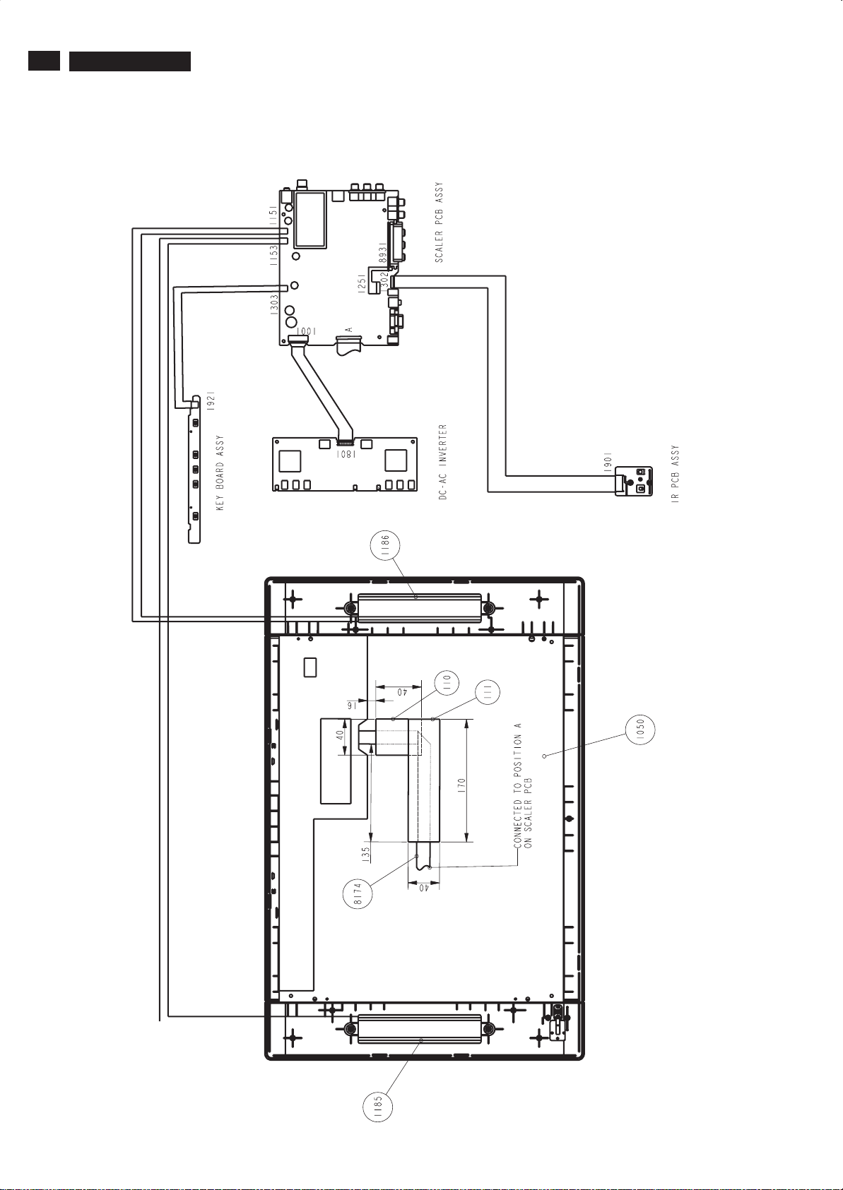
Step 4. Remove the YPbPr-IN,Scaler, KEY ,IR and inverter board.
a).Remove the 2 screws and disconnect the 10 cables as Fig. 10
to remove the YPbPr-IN board.
b).Remove the 4 screws and disconnect the connector as Fig.11
to remove the scaler board.
c).Remove the 2 screws and disconnect the connector as Fig.12
to remove the inverter board.
d).Remove the screw and disconnect the connector as Fig.13 to
remove the IR board.
Page 7
4. Mechanical Instructions
e). Remove the control board and open the click ,disconnect the
connector as Fig.14-Fig.15
TPF1.3A LA
7
Fig.11
Fig.12
Fig.15
Step 5. Remove the 4 screws as Fig.16 to remove the speaker
Fig. 16
Fig.17
Fig. 14
Fig. 13
Set Re-assembly
To re-assemble the whole set, execute all processes in reverse
order.
Notes:
a. While re-assembling, make sure that all cables are placed
and connected in their original position.
b. Pay special attention not to damage the EMC foams at the
SSB shielding. Check that EMC foams are put correctly on
their places.
In warranty, it is not allowed to disassembly the LCD panel, even the
backlight unit defect.
Out of warranty, the replacment of backlight unit is a correct way
when the defect is cused by backlight (CCFL,Lamp).
Page 8
8
TPF1.3A LA
5. Aging and Factory Mode
5. Aging and Factory Mode
index of this chapter:
5.1 Access Aging Mode
5.2 Access Factory Mode
Top Control
-
Volume
Left
<B> <C> <D> <E> <F>
Right
+
Menu
-
Channel
+
UpDown
Front Control
Power SW
<A>
LED
RC sensor
5.1 Access Aging Mode
Step 1 : D
Step 2 :
quickly push " + "and "-"ofVolume,and hold this two buttons
comes out " AGING screen"] => then release all buttons.
Bring up:
isconnect Interface Cable between Monitor and PC.
Turn off LCD monitor.Then press power " " button.Then
AGING...
untill
5.2 Access Factory Mode
1). Turn off monitor.
2).
Press power " " button.Then quickly push " + " and " - "of
Volume ,and hold this two buttons , then the screen comes out
"Waiting For Automatic Adjustment ",then the screen will be black
for one second untill comes out "Windows screen"] => then
release this two buttons.
3). Press "MENU" button, wait until the OSD menu with
Characters "CHINA MAGNAVOX32 V0.2.0 051012
CLAA320WA01" (below OSD menu) come on the Screen
of the monitor.
Factory Mode indicator
Factory Menu
Cursor can move on gray color area
Hot key function: at factory mode , press "MENU" button,then press
"+"and"-"ofChannel to the factory mode indicator ,then press
" + " of Volume .Press the " + " and "-"ofChannel to "exit " and
press "MENU" to exit factory adjust menu.
After 52 seconds,
bring up:
AGING...
After 60 seconds,
bring up:
AGING...
After 52 seconds,
bring up:
----------
---------repeatly
Connect Signal cable again=> go back to normal display
Page 9
10
TPF1.4A LA
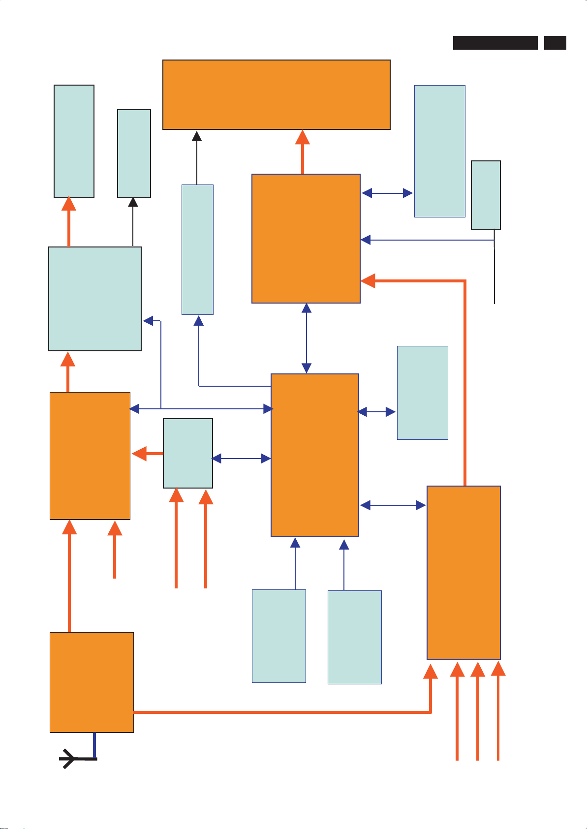
6. Block Diagram
Index of this chapter:
6.1
Wiring Diagram
6.2 Block Diagram
6.1 Wiring Diagram
6. Block Diagram
Page 10
10
6.2 Main board block diagram
TPF1.3A LA
S-L
TPA3005D2
Audio AMP
S-G
K
6. Block Diagram
IR and key pad
Control Board
S-H
Panel
LVDS
SCALER
MST51502
MSP_OUT_L/R
S-K
IF
nd
2
EEPROM
MSP3415G
Sound decoder
PC audio
x8
4K
S-G
D
M
S-I
MCU
NT68F632
SDRAM
IIC
DDC
512Kx16x2
PC analog
...
VY[0… 7]
YPbPr (HD)
S-E
SAA7119E/V2
Video Decoder
X
audio
Tuner
video
SC -audio
S_Audio
Tuner CVBS
SVHC_YC
AV CVBS
YPbPr_RGB_SC
Page 11
INVERTER BLOCK DIAGRAM
6. Block Diagram
P
TPF1.3A LA
11
12VDC
Page 12
12
TPF1.3A LA
INVERTER FUNCTION BLOCK DIAGRAM
6. Block Diagram
P
Page 13
6. Block Diagram
Scalar board
Panel
TPF1.3A LA
13
Speakers
AMP
Audio
Output
TPA3005
LVDS
1Mx16
SDRAMÁ 2
DDC
Scaler
MST51512
BL controller
PC Analog
24C32
Eeprom
Sound
Decoder
IF
nd
2
Tuner
MSP3415
PC audio
FQ1256/I
MUX
AV / S -Video audio
YPbPr(HD) audio
IR
OFF/ON
Tuner CVBS
MCU
NT68F632A(128KB)
Board
Control
SAA7119
Video Decoder
YPbPr(HD)
S-video
AV
Page 14

14
TPF1.4A LA
FFC
6. Block Diagram
S-Video
Sound
Decoder
AV L/R
Panel
Audio
Decoder
Scaler IC
YPbPr L/R
PC Audio
DSub
DC in
In
Inverter
Adapter
Page 15
Index of this chapter:
7.1 Chassis Overview
7.2 Exploded View
7.3 Scaler Schematic Diagram & Layouts
7.4 Power Schematic Diagram & Layouts
7.5 Key PCB Schematic Diagram & Layouts
7.6 IR PCB Schematic Diagram & Layouts
7.7 YPbPr-IN PCB Schematic Diagram & Layouts
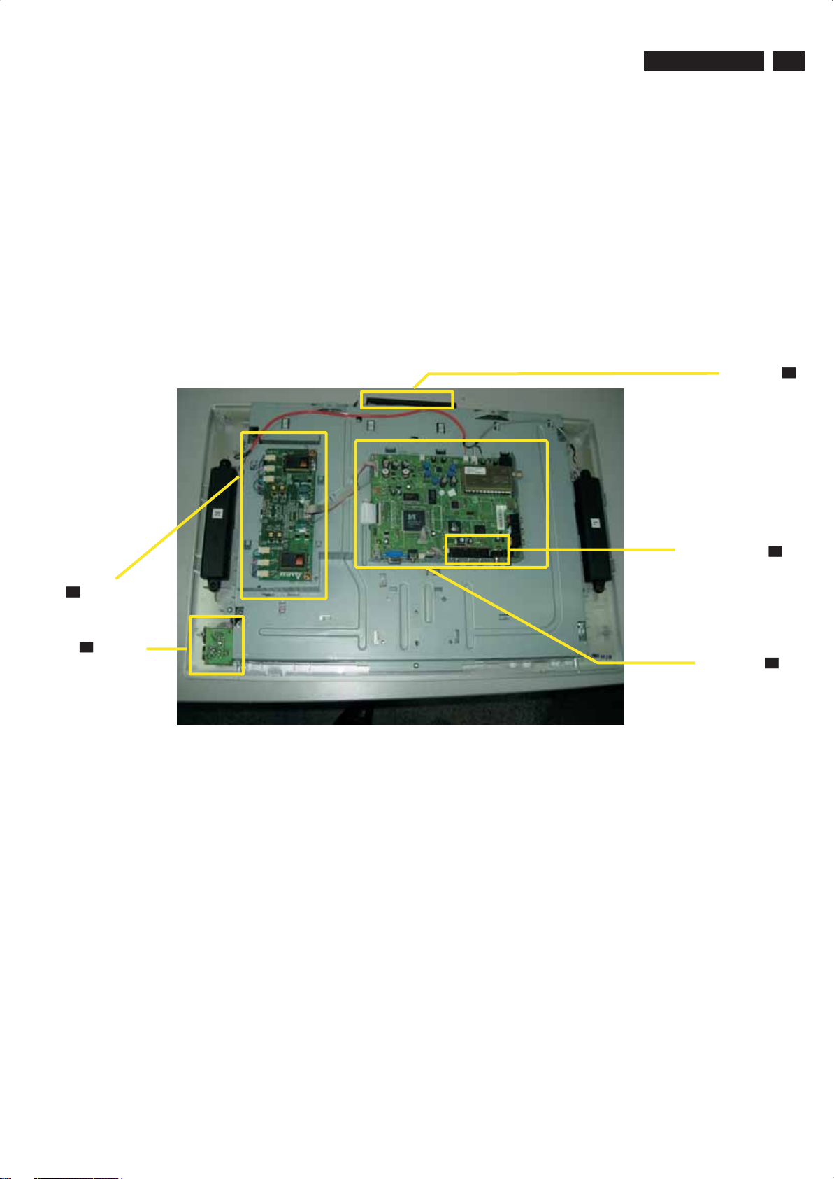
7.1 Chassi Overview
7.Circuit Diagram & PWB Layouts
TPF1.3A LA
15
Innverter Board
P
I
IR Board
Key Board
YPbPr-IN Board
Scaler Board
K
Y
S
Page 16
16
TPF1.3A LA
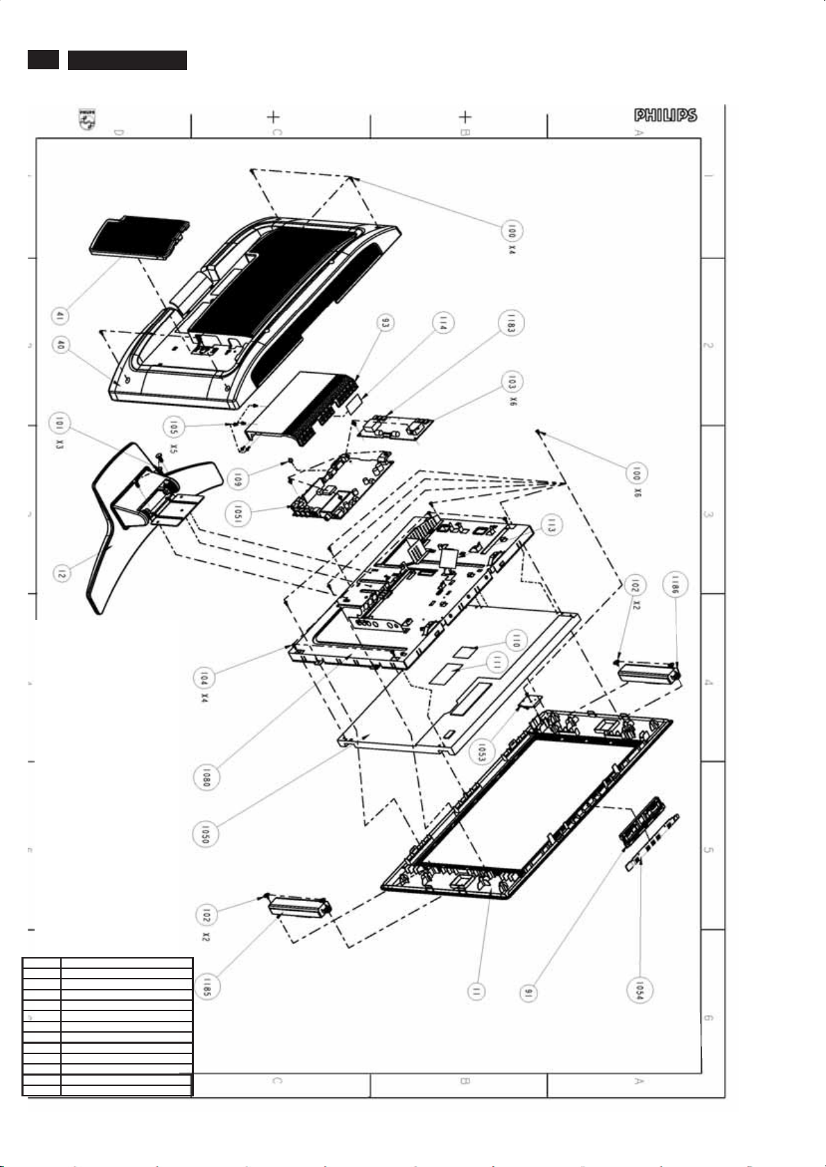
7.2 Exploded View
7. Circuit Diagrams and PWB Layouts
0011 BEZEL ASSY
0040 BACK COVER
0041 DOOR-CABLE
0091 CONTROL BUTTON
0093 SHIELD - SCALER
0109 NUT-AUDIO JACK
1050 TFT-LCD A201SN02V4 (AUOP) B
1051 SCALER ASSY(CHINA 20 AUO)
1053 KEY BOARD ASSY
1054 IR PCB ASSY
1183 PSU OPENFR INV BL6 (DAC-16T003
1185 LSP BOX 8R 3W - R (P 150CR)
1186 LSP BOX 8R 3W - R ( P150CL)
Page 17
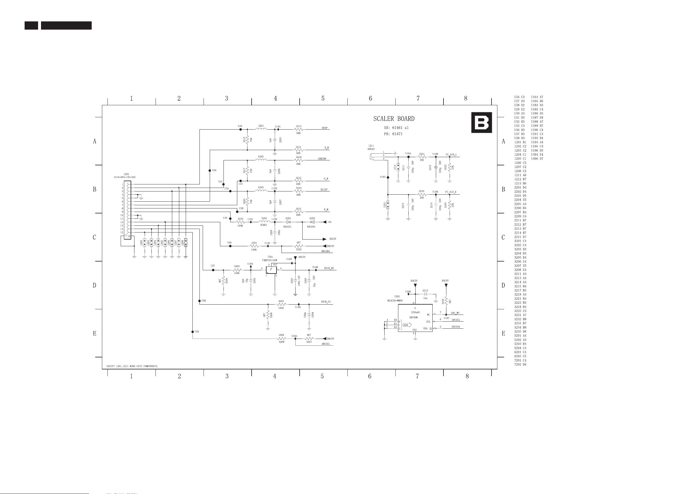
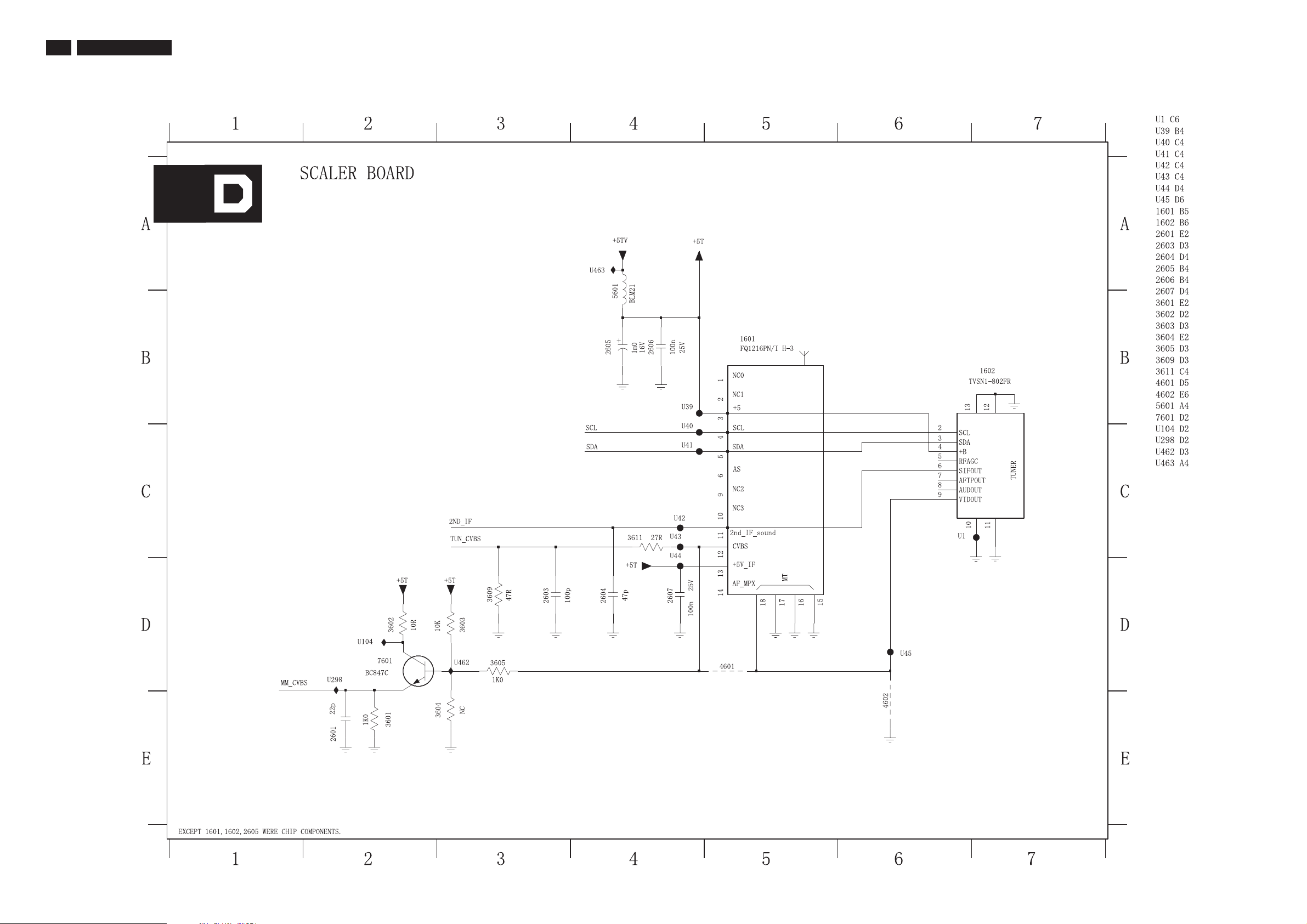
7.3.1 Scaler Schematic Diagram - power
7.Circuit Diagrams and PWB Layouts
S-
TPF 1.3A LA
17
Page 18
18
TPF 1.3A LA
7.3.2 Scaler Schematic Diagram - PC IN
7. Circuit Diagrams and PWB Layouts
Page 19
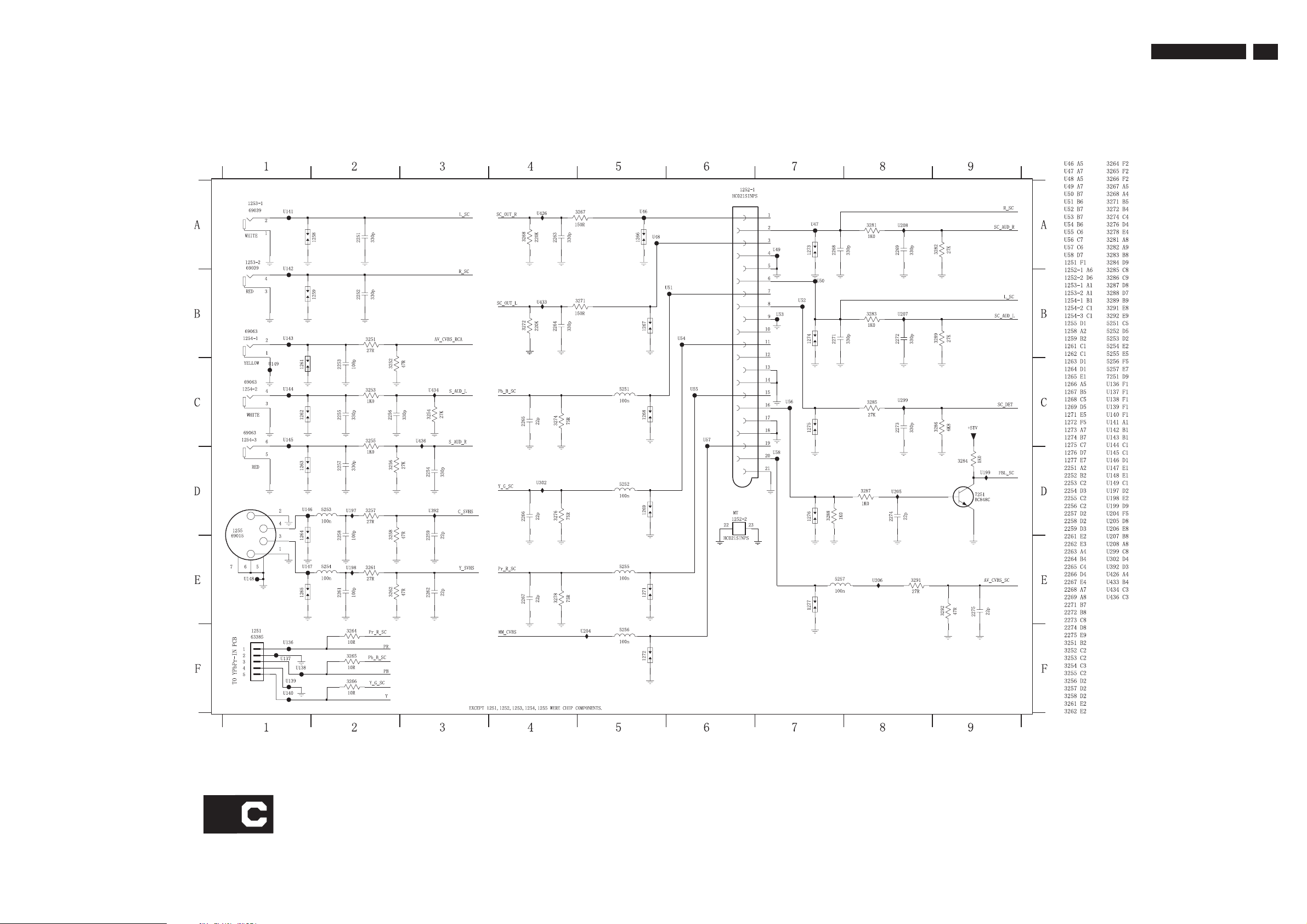
7.3.3 Scaler Schematic Diagram - SCART
7. Circuit Diagrams and PWB Layouts
TPF 1.3A LA
19
S-
Page 20
20
7.3.4 Scaler Schematic Diagram - VIDEO IN
TPF 1.3A LA
S-
7. Circuit Diagrams and PWB Layouts
Page 21
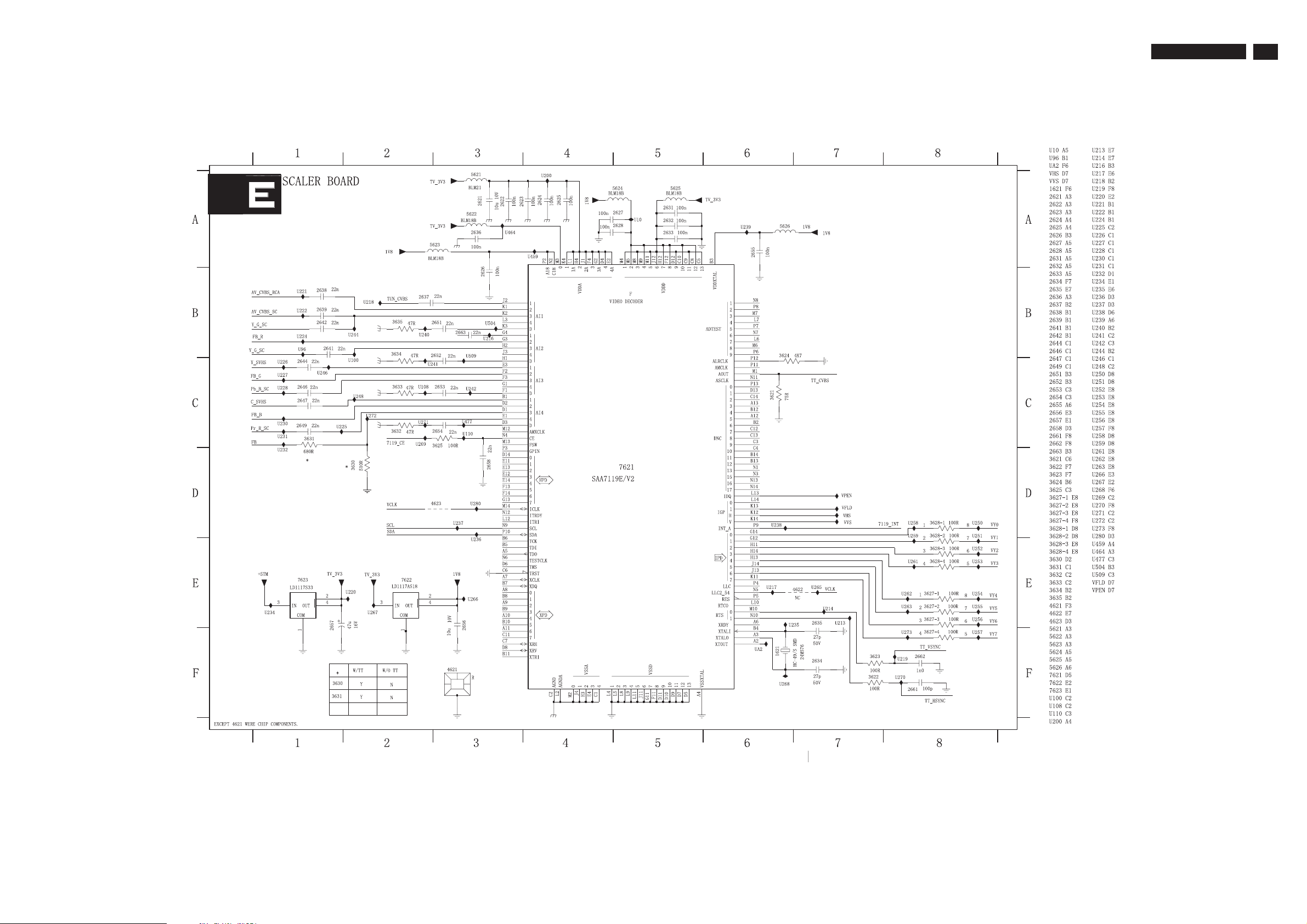
7.3.5 Scaler Schematic Diagram - VIDEO DECODER
S-
7. Circuit Diagrams and PWB Layouts
TPF 1.3A LA
21
Page 22
22
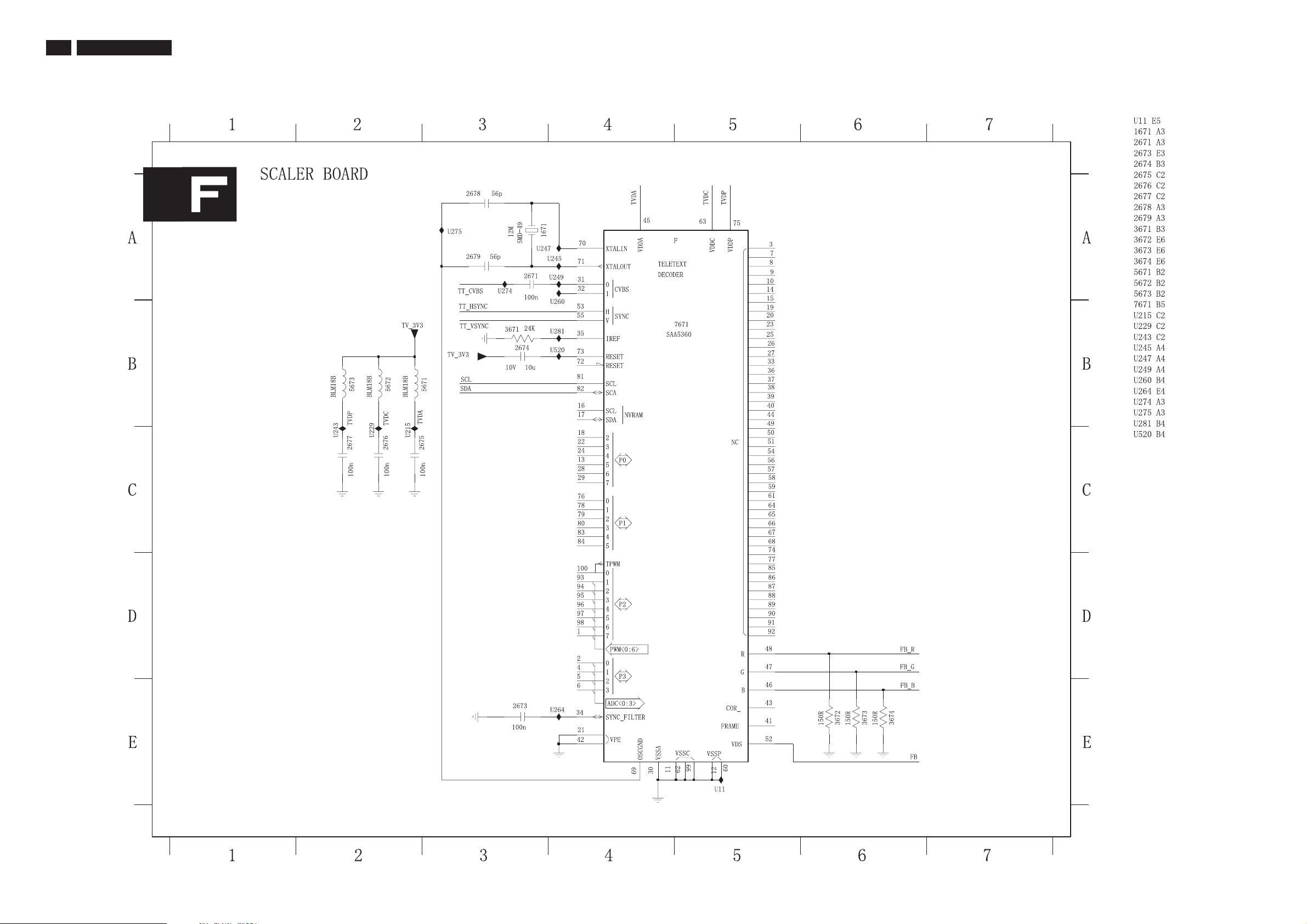
7.3.6 Scaler Schematic Diagram - T/T DECODER
TPF 1.3A LA
S-
7.Circuit Diagrams and PWB Layouts
Page 23
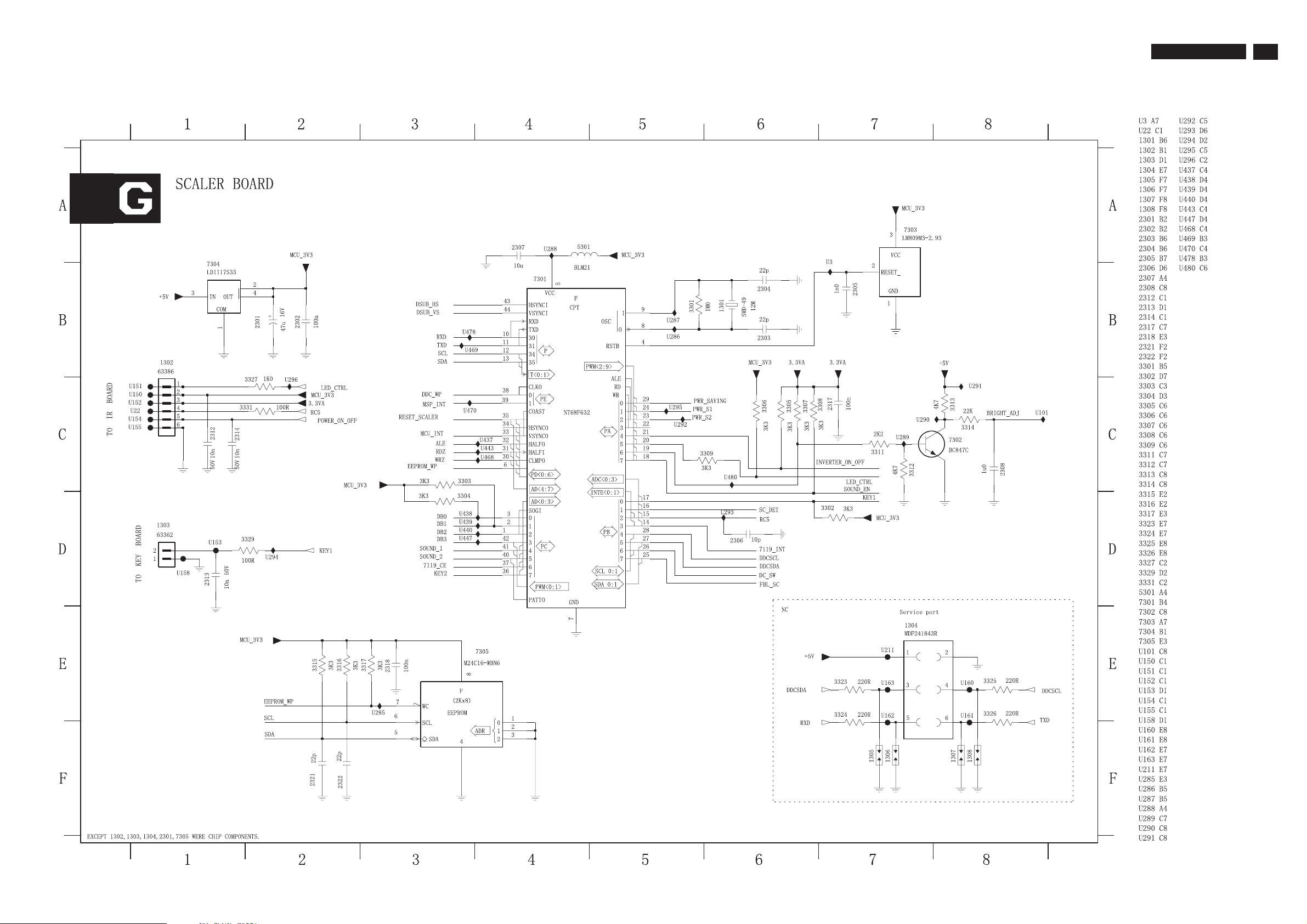
7.3.7 Scaler Schematic Diagram - MCU
S-
7. Circuit Diagrams and PWB Layouts
TPF 1.3A LA
23
Page 24
24
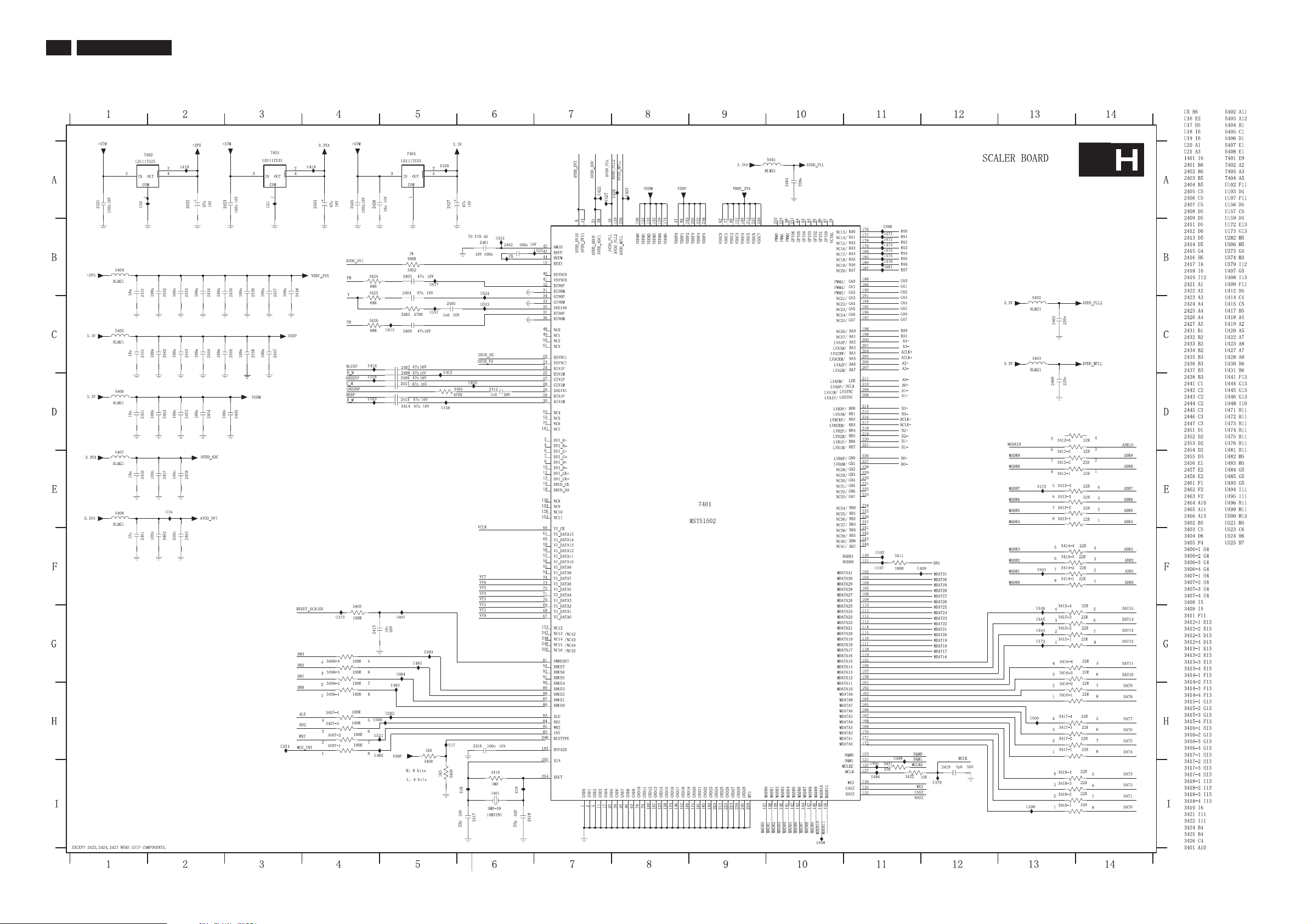
7.3.8 Scaler Schematic Diagram - SCALER
TPF 1.3A LA
7. Circuit Diagrams and PWB Layouts
S-
Page 25

7.3.9 Scaler Schematic Diagram - SRAM
7. Circuit Diagrams and PWB Layouts
S-I
TPF 1.3A LA
25
Page 26

26
7.3.10 Scaler Schematic Diagram - Panel Interface
TPF 1.3A LA
7. Circuit Diagrams and PWB Layouts
S-J
Page 27

7.3.11 Scaler Schematic Diagram - SOUND DECODER
S-K
7. Circuit Diagrams and PWB Layouts
TPF 1.3A LA
27
Page 28

28
7.3.12 Scaler Schematic Diagram - AUDIO
TPF 1.3A LA
S-L
7. Circuit Diagrams and PWB Layouts
Page 29

7.3.13 Scaler Board Layout-1
7. Circuit Diagrams and PWB Layouts
TPF 1.3A LA
29
Page 30

30
TPF 1.3A LA
7.3.14 Scaler Board Layout-2
7. Circuit Diagrams and PWB Layouts
Page 31

7.4.1 Inverter Schematic Diagram
7. Circuit Diagrams and PWB Layouts
TPF 1.3A LA
31
Page 32

32
7.5 Key Board Schematic Diagram
TPF1.3A LA
K
7. Circuit Diagrams and PWB Layouts
Page 33

7.5 Key PCB Layout-1
7.Circuit Diagram & PWB Layouts
TPF1.3A LA
33
Page 34

34
7.5 Key PCB Layout-2
TPF1.3A LA
7. Circuit Diagrams and PWB Layouts
Page 35

7.6 IR PCB Schematic Diagram
I
7.Circuit Diagram & PWB Layouts
TPF1.3A LA
35
Page 36

36
TPF1.3A LA
7.6 IR PCB Layout-1
7. Circuit Diagrams and PWB Layouts
Page 37

7.6 IR PCB Layout-2
7.Circuit Diagram & PWB Layouts
TPF1.3A LA
37
Page 38

38
7.7 YPbPr-IN PCB Schematic Diagram
TPF1.3A LA
Y
7. Circuit Diagrams and PWB Layouts
Page 39

7.7 YPbPr-IN PCB Layout-1
Y
7.Circuit Diagram & PWB Layouts
TPF1.3A LA
39
Page 40

40
TPF1.3A LA
7.7 YPbPr-IN PCB Layout-2
7. Circuit Diagrams and PWB Layouts
Page 41

8. Alignments
TPF1.3A LA
41
8. Alignments
index of this chapter:
8.1 Electrical Instructions
8.2 DDC Instructions&Serial NO. Definition
8.3 DDC DATA
8.4 ISP Instructions
8.5 Display Adjustment
8.1 Electrical Instructions
1. General points
1.1 During the test and measuring, supply a distortion free AC mains
Voltage to the apparatus via an isolated transformer with low
internal resistance.
1.2 All measurements mentioned hereafter are carried out at a normal
mains voltage (90 - 132 VAC for USA version, 195 -264 VAC for
EUROPEAN version, or 90 - 264 VAC for the model with full range
power supply, unless otherwise stated.)
1.3 All voltages are to be measurement or applied with respect to
ground,unless otherwise stated.
Note: Don‘t use heat-sink as ground.
1.4 The test has to be done on a complete set including LCD panel
in a room with temperature of 25 +/- 5 degree C.
1.5 All values mentioned in these test instruction are only applicable
of a well aligned apparatus, with correct signal.
2.2 PC Input signal mode
PRE-LOAD VIDEO RESOLUTION
Mode 3, 6, 7 are preset modes that should pass QA inspection.
Mode 1, 2, 4, 5, 8 wil l r un aut o adjus tment o nly, and W/O QA
checking.
Dot rate (MHz) H.fr eq
(KHz)
1 25.175 31.469 IBM VGA 640 * 350 70.087
2 28.322 31.469 IBM VGA 720 * 400 70.087
3 25.175 31.469 IBM VGA 640 * 480 59.940
4 30.240 35.000 MACINTOSH 640 * 480 66.667
5 31.500 37.500 VESA 640 * 480 75.000
6 36.000 35.156 VESA 800 * 600 56.250
7 40.000 37.879 VESA 800 * 600 60.317
8 49.500 46.875 VESA 800 * 600 75.000
2.3 TV input signal Channel and pattern for China model (1)
Signal Distribution Table (PAL D)
Frequency Carriers
PRG CH
Video Sound
Mode Resolution V.freq (Hz)
TV System
Pattern
1.6 The letters symbols (B) and (S) placed behind the test instruction
denotes
(B): carried out 100% inspection at assembly line
(S): carried out test by sampling
1.7 The white balance (color temperature), has to be tested in subdued
Lighted room.
1.8 Repetitive power on/off cycle are allowed except it should be avoided
within 6 sec.
2. Input signal
---------------
2.1.1 PC Signal type
Analog Video : 0.7 Vp-p linear, positive polarity
Separate Sync. : TTL level, separate, positive or negative polarity
Audio signal : Mini-jack audio input
Input level: 500 mVrms (Speaker outpout 3W when Input level
> 630mVrms and Volume control at 100%)
TV Signal type
RF Signal : Aerial input, NTSC cable and antenna system.
Video signal : Cinch input, CVBS with NTSC and PAL system.
Level: 1.0Vp-p (0.7V video + 0.3V sync.)
S video input: Y/C signal, NTSC and PAL system.
Level: Y: 1.0Vp-p (0.7V video + 0.3V sync.)
C: +/- 0.3V.
Component input: Cinch G/B/R-> YPbPr cinch input.
Level: Y: 1.0Vp-p Pb/Pr: +/- 0.35V
Audio signal : Side cinch R/L for CVBS and S-video
Bottom cinch R/L for component input.
Input level: 500 mVrms (Speaker outpout 3W when Input level
> 630mVrms and Volume control at 100%)
C4 65.25MHz 71.75MHz
1
E7 184.25MHz 190.75MHz
2
E12 224.25MHz 230.75MHz
3
K21 471.25MHz 477.75MHz
4
G34 511.25MHz 517.75MHz
5
G62 547.25MHz 553.75MHz
6
M58 551.25MHz 557.75MHz
7
8
G47 615.25MHz 621.75MHz
PAL D
(CCIR)
PAL D
(CCIR)
PAL D
(CCIR)
PAL D
(CCIR)
PAL D
(CCIR)
PAL D
(CCIR)
PAL D
(CCIR)
PAL D
(CCIR)
Full Write
Circle
Pattern
Color Bar
Full Write
Circle
Pattern
Color Bar
Crosshatch
Color Bar
Table 1
Page 42

42
TPF1.3A LA
8. Alignments
3. TV mode display adjustment
3.1 White balance adjustment (B)
General set-up :
Equipment Requirements: Color analyzer.
Input requirements:
Input Signal Type : CVBS-PAL signal.
Frequency = 65.25 MHz (for China model).
Alignment method:
Initial Set-up : Set TV (7119) Brightness=120;
Contrast=70, Saturate=73,Tint=24 in
factory mode (can be fine tuned)
Set Smart picture as PERSONAL (Brightness=50,
Color=50, Contrast=50)
""
Apply 100IRE (100%) Full White pattern by TV pattern generator.
Alignment: Adjust the VIDEO SCALER GAIN R G B in Factory Mode
""
For NORMAL , COOL and WARM . (See Fig 1.)
[ Enter factory menu : press Volume - and Menu keys together
around six seconds]
Keep R=121 for the adjustment of NORMAL , COOL and WARM .
""
""""
""""
""
""
""
The 1931 CIE chromaticity (X, Y) co-ordinates shall be:
Picture Mode x y
Normal
Cool
Warm
0.287 ± 0.005 0.287 ± 0.005
0.275± 0.005 0.270± 0.005
0.315± 0.005 0.310± 0.005
Table 3.1: Readings with Minolta CA-110.
Gains NORMAL COOL WARM
R 127 119 128
G 118 109 111
B 114 112 91
4.3 Check the analog interface cable
Check the color poor & noise condition of 64-gray pattern.
5. HD mode display adjustment
5.1 White balance adjustment (B)
General set-up:
Equipment : Quantum Data Pattern Generator 801GD or 802G.
Apply 1080i, RGBW gray pattern.
FACTORY ADJUST MENU
NORMAL
SCALER GAIN R G B
AUTO-COLOR (OK)
ADC OFFSET R G B
ADC GAIN R G B
PC OFFSET R G B
7119 SDTV ? SAT TINT
TV SHIFT H V
HD SHIFT H V
RESERVE
HDTV ADC OFFSET R G B
HDTV ADC GAIN R G B
VIDEO SCALER GAIN R G B
SCALER HUE
EXIT Value
Fig-1
4.PC mode display adjustment
4.1 Display quality adjustment
Use timing mode as describe in 2.2, and use the POPO (pixel
on pixel off) pattern to adjust the clock until no stripe and
adjust the phase until clear picture.
(AUTO ADJUST hot key: press Volume- and Menu keys together
""
""
for 1 second.)
Check the 3 preset modes.
4.2 WHITE-D adjustment (B)
(Or FLUKE 54200, apply 576i, DIGITAL SCAN/DIGI_ADC1 pattern.)
Alig nment m ethod:
Initial Set-up: Set SA7119 as, Brightness=120;Saturation=70;
Contrast=73;Tint=24
Set Smart picture as Personal , Brightness=50,
""
Color=50, Contrast=50
Set AUTO-COLOR process.
Alignments: Make the VIDEO SCALER GAIN R G B same as TV mode.
Check chromaticity (X, Y) co-ordinates specification:
4.2.1 At factory mode apply 800x600/60Hz mode with 64 gray pattern.
Set main controls brightness control at 50% and contrast to 50% .
Select AUTO-COLOR function for ADC OFFSET and ADC GAIN
setup.
4.2.2 Set SCALER GAIN R G B
""
of NORMAL COOL and WARM
""
""
as:
Picture Mode x y
Personal/Normal
0.287 ± 0.015 0.287 ± 0.015
If out of specification, fine-tune HDTV ADC GAIN in factory mode
Page 43

8. Alignments
6. Preset EEPROM data
6.1 EEPROM data has to be preset data according following table.
Factory mode preset.
Function
SCALER GAIN
ADC Offset R/G/B
ADC Gain R/G/B
PC OFFset R/G/B
7119 brightness
PC Normal 127 118 114
PC Cool 119 109 112
PC Warm 128 111 91
120 (RF) 120(AV/SVHS/HD)
Preset value
127 127 127
127 127 127
127 127 127
TPF1.3A LA
HD(YPbPr) RICH NATURE SOFT MULTMEDIA PERSONAL
Brightness 48 40 30 46 50
Color 75 70 55 80 50
Contrast 60 57 57 67 50
Sharpness 79 58 58 87 50
Smart Sound
43
7119 Saturation
7119 contrast
7119 TINT
TV shift H
TV shift V
HD SHIFT H
HD SHIFT V
HD ADC OFFset R G B
HD ADC GAIN R G B
Video Scaler Gain
Scaler Hue
Factory mode:
6.2 Smart picture &Smart sound:
Regular
75 (RF) 70(AV/SVHS/HD)
75 (RF)
24 (RF) 24(AV/SVHS/HD)
73(AV/SVHS/HD)
NTSC PAL
146 162
914
##
##
127 127 127
127 127 127
127 127 127
50
Smart Sound : THEATRER
Sound volume :20
Incredible surround: OFF
AVL : OF F
6.2.1 Final TV mode out box setting.
RF channel: Channel 1
Format: 4:3
Language: Chinese
Smart picture: RICH(Cool)
Smart Picture
RF RICH NATURE SOFT MULTMEDIA PERSONAL
Brightness 43 40 39 50 50
Color 60 57 52 70 50
Contrast 60 50 45 56 50
Sharpness 41 33 29 50 50
AV/S-Video RICH NATURE SOFT MULTMEDIA PERSONAL
Brightness 40 38 35 45 50
Color 52 54 49 63 50
Contrast 60 52 45 60 50
Sharpness 75 58 50 70 50
Page 44

44
TPF1.3A LA
8. Alignments
8.2 DDC Instructions&Serial NO. Definition
General
DDC Data Re-programming
In case the DDC data memory IC or main EEPROM which storage all
factory settings were replaced due to a defect, the serial numbers have
to be re-programmed "Analog DDC IC, Digital DDC IC & EEPROM".
It is advised to re-soldered DDC IC and main EEPROM from the old
board onto the new board if circuit board have been replaced, in this case
the DDC data does not need to be re-programmed.
Additional information
Additional information about DDC (Display Data Channel) may be
obtained from Video Electronics Standards Association (VESA).
Extended Display Identification Data(EDID) information may be also
obtained from VESA.
System and equipment requirements
1. An i486 (or above) personal computer or compatible.
2. Microsoft operation system Windows 95/98 .
Y o Install the EDID_PORT_Tool under Win2000/XP . As
ou have t
Fig. 1 .
Note: The alignment box has already build-in a batteries socket for
using batteries (8~12V) as power source. Pull out the socket by
remove four screws at the rear of box. Please do not forget that
remove batteries after programming. The energy of batteries can
only drive circuits for a short period of time.
Pin assignment
A. 15-pin D-Sub Connector
PIN No. SIGNAL
1Red
2Green
3Blue
4GND
5GND
6RedGND
7GreenGND
8BlueGND
9 +5V (Supply from PC)
10 Sync GND
11 GND
12 Bi-directional data
13 H-sync
14 V-sync
15 Data clock
A. Cody the "UserPort.sys" to C:\WINNT\system32\drivers(win2000)
C:\WINDOWS\system32\drivers(winXP)
B. Running " io.exe" everytime, Before you start to programming
edid data .
3. EDID46.EXE program
4. A/D Alignment kits (12NC: 3138 106 10396):
inclusion : a. Alignment box x1 (Fig. 2)
Fig.1
b. Printer cable x1
c. (D-Sub) to (D-Sub) cable x1
Fig. 2
Page 45

8. Alignments
TPF1.3A LA
45
Configuration and procedure
There is no Hardware DDC (DDC IC) anymore. Main EEPROM stores
all factory settings and DDC data (EDID code) which is also called
Software DDC. The following section describes the connection and
procedure for Software DDC application. The main EEPROM can be reprogrammed by enabling '' factory memory data write'' function on the
DDC program (EDID46.EXE).
Initialize alignment box
In order to avoid that monitor entering power saving mode due
to sync will cut off by alignment box, it is necessary to initialize
alignment box before running programming software
(EDID46.EXE). Following steps show you the procedures and
connection.
Step 1: Supply 8-12V DC power source to the Alignment box by
plugging a DC power cord .
Step 2: Connecting printer cable and D-Sub cable of monitor as Fig. 4
PC
1= Power connector
2= D-SUB connector
3. At the submenu, type the letter of your computer's hard disk drive
followed by :EDID46 (for example, C:\EDID46, as shown in Fig. 6).
1
Fig. 6
4. Click OK button. The main menu appears (as shown in Fig. 7).
This is for initialize alignment box.
DC Power
8-12 V
----->
2
To printer port (LTP1)
Printer
Port
To
Monitor
To P C
----->
1
Fig. 4
Step 3: Installation of EDID46.EXE
Method 1: Start on DDC program
Start Microsoft Windows.
1. The Program"EDID46.EXE" in service manual cd-rom be copyed to C:\ .
2. Click , choose Run at start menu of Windows as shown
In Fig. 5.
Fig. 5
Fig. 7
Note 1: If the connection is improper, you will see the following error
message (as shown in Fig. 8) before entering the main menu.
Meanwhile, the (read EDID) function will be disable. At this
time, please make sure all cables are connected correctly and
fixedly, and the procedure has been performed properly.
Fig. 8
Note 2: During the loading, EDID46 will verify the EDID data which just
loaded from monitor before proceed any further function, once
the data structure of EDID can not be recognized, the following
error message will appear on the screen as below. Please
confirm following steps to avoid this message.
1. The data structure of EDID was incorrect.
2. DDC IC that you are trying to load data is empty.
3. Wrong communication channel has set at configuration setup
windows.
4. Cables loosed or poor contact of connection.
Fig. 9
Page 46

46
TPF1.3A LA
Re-programming Analog DDC IC
Step 1: After initialize alignment box, connecting all
cables and box as shown in Fig. 10.
PC
1= Power connector
2= D-SUB connector
8. Alignments
DC Power
8-12V
To printer port (LTP1)
To P C Video port (D-sub)
Printer
Port
To
Monitor
To P C
1
2
----->
----->
Step 2: Read DDC data from monitor
1. Click icon as shown in Fig. 11 from the tool bar to bring up
the Channels "Configuration Setup" windows as shown in Fig. 11.
=====>
Click this button
Fig. 11
2. Select the DDC2Bi as the communication channel.
As shown in Fig. 12.
Fig. 10
Fig. 13
Step 3: Modify DDC data (verify EDID version, week,
year)
Click (new function) icon from the tool bar, bring up
Step 1 of 9 as shown in Fig. 14 .
EDID46 DDC application provides the function selection and
text change (select & fill out) from Step 1 to Step 9.
Select and fill out,
If necessary.
Fig. 14
Step 4: Modify DDC data (Monitor Serial No.)
1. Click Next , bring up Fig. 15.
Fig. 12
3. Click OK button to confirm your selection.
4. Click icon (Read EDID function) to read DDC EDID data from
monitor. The EDID codes will display on screen as shown in Fig. 13.
Fig. 15
Page 47

2. Click Next , bring up Fig.16.
8. Alignments
5. Click Next , bring up Fig.19.
Fig. 16
TPF1.3A LA
47
Fig. 19
3. Click Next , bring up Fig.17.
4. Click Next , bring up Fig.18.
6. Click Next , bring up Fig. 20.
In this step, you can modify the SN as below.
Fig. 17
Fig. 20
7. Click Next , bring up Fig. 21.
Fig. 18
Fig. 21
Page 48

48
8. Click Next , bring up Fig. 22.
TPF1.3A LA
- Click Finish to exit the Step window.
- Serial number can be filled up at this moment (for example,
923418).
8. Alignments
4). Click (Write EDID) icon from the tool bar to write DDC data.wait
for 5 seconds ,DDC data will be finished Writing.
Step 6: Save DDC data
Sometimes, you may need to save DDC data as a text file
for using in other IC chip. To save DDC data, follow the
steps below:
1. Click (Save) icon (or click "file"-> "save as") from the tool
bar and give a file name as shown in Fig. 25.
The file type is EDID46 file (*.ddc) which can be open in
WordPad. By using WordPad, the texts of DDC data & table
(128 bytes, hex code) can be modified. If DDC TEXTS &
HEX Table ar completely correct, it can be saved as .ddc flie
to re-load it into DDC IC for DDC Data application.
Step 5: Write DDC data
1. Configuration should be as Fig. 23. And press OK.
Fig. 22
Fig. 23
20TA1000
20TA1000 analog
Fig. 25
2. Click Save.
Step 7: Exit DDC program
Pull down the File menu and select Exit as shown in Fig. 26.
2. Access Factory Mode
1). Turn off monitor.
2).
Press power " " button.Then quickly push"+"and"-"of
Volume ,and hold this two buttons , then the screen comes out
"Waiting For Automatic Adjustment ",then the screen will be black
for one second untill comes out "Windows screen"] => then
release this two buttons.
3). Press "MENU" button, wait u ntil the OSD menu appears
(See Fig.24).
Fig. 24
----------------->
Factory Mode
3) Push Menu to exit OSDmenu.""
Step 8: Turn off the monitor, exit the factory mode.
Fig. 26
Serial NO. definition
Indicator
Page 49

8. Alignments
TPF1.3A LA
49
8.3 DDC DATA
Display data channel : DDC2B
DDC DATA
Use a computer with DDC communication capability to read the
DDC2B display identification data from the monitor.
AUO panel:
**********************************************************************
EDID log file
**********************************************************************
Vendor/Product Identification
ID Manufacturer Name : PHL
ID Product Code : 4650 (HEX.)
ID Serial Number : 1010101 (HEX.)
Week of Manufacture : 39
Year of Manufacture : 2005
EDID Version, Revision
Version : 1
Revision : 3
Basic Display Parameters/Features
Video Input Definition : Analog Video Input
0.700V/0.300V (1.00Vpp)
without Blank-to-Black Setup
Separate Sync
without Composite Sync
without Sync on Green
no Serration required
Maximum H Image Size : 41
Maximum V Image Size : 31
Display Transfer Characteristic : 2.4
(gamma)
Monitor Descriptor #3
Monitor Name : PHL TA1000
Monitor Descriptor #4
Monitor Range Limits
Min. Vt rate Hz : 56
Max. Vt rate Hz : 62
Min. Horiz. rate kHz : 30
Max. Horiz. rate kHz : 40
Max. Supported Pixel : 40
No secondary GTF timing formula supported.
Extension Flag : 0
Check sum : AF (HEX.)
***********************************************************
EDID data (128 bytes)
***********************************************************
0: 00 1: ff 2: ff 3: ff 4: ff 5: ff 6: ff 7: 00
8: 41 9: 0c 10: 50 11: 46 12: 01 13: 01 14: 01 15: 01
16: 27 17: 0f 18: 01 19: 03 20: 08 21: 29 22: 1f 23: 8c
24: ee 25: fc 26: 60 27: a5 28: 55 29: 4a 30: 9c 31: 23
32: 10 33: 46 34: 4b 35: 23 36: 00 37: 00 38: 01 39: 01
40: 01 41: 01 42: 01 43: 01 44: 01 45: 01 46: 01 47: 01
48: 01 49: 01 50: 01 51: 01 52: 01 53: 01 54: 00 55: 00
56: 00 57: ff 58: 00 59: 0a 60: 20 61: 20 62: 20 63: 20
64: 20 65: 20 66: 20 67: 20 68: 20 69: 20 70: 20 71: 20
72: 00 73: 00 74: 00 75: ff 76: 00 77: 0a 78: 20 79: 20
80: 20 81: 20 82: 20 83: 20 84: 20 85: 20 86: 20 87: 20
88: 20 89: 20 90: 00 91: 00 92: 00 93: fc 94: 00 95: 50
96: 48 97: 4c 98: 20 99: 54 100: 41 101: 31 102: 30 103: 30
104: 30 105: 0a 106: 20 107: 20 108: 00 109: 00 110: 00 111: fd
112: 00 113: 38 114: 3e 115: 1e 116: 28 117: 04 118: 00 119: 0a
120: 20 121: 20 122: 20 123: 20 124: 20 125: 20 126: 00 127: af
Feature Support (DPMS) : Standby
Display Type : RGB color display
Standard Default Color Space : Primary color space
Preferred Timing Mode : Detailed timing block 1
Color Characteristics
Red X coordinate : 0.647
Red Y coordinate : 0.335
Green X coordinate : 0.292
Green Y coordinate : 0.609
Blue X coordinate : 0.138
Blue Y coordinate : 0.064
White X coordinate : 0.273
White Y coordinate : 0.293
Established Timings
Established Timings I : 640 x 480 @60Hz (IBM,VGA)
800 x 600 @56Hz (VESA)
800 x 600 @60Hz (VESA)
Established Timings II :
Manufacturer's timings :
Standard Timing Identification : Unused
Monitor Descriptor #1
Serial Number :
Suspend
Active Off
Monitor Descriptor #2
Serial Number :
Page 50

50
TPF1.3A LA
8.4 ISP Instructions
Configuration and procedure
"Easywriter " The software is provided by Novatek to upgrade the
firmware of CPU.
It is a windows-based program, which cannot be run in MS-DOS.
DDC2BI_ISP TOOL (3138 149 53161) is for the interface between
"Parallel Port of PC" and "15 pin-D-SUB connector of Monitor".
8. Alignments
System and equipment requirements
1. An i486 (or above) personal computer or compatible.
2. Microsoft operation system Windows 95/98/2000/XP.
3. ISP Software " Easywrite "
4. as shown in Fig. 1
DDC2BI_ISP TOOL (3138 106 10396)
D-SUB to monitor
Parallel Port to Print Port in PC
Fig. 1
5. Connect and Mains cord to Monitor as shown
in Fig. 2.
DDC2BI_ISP TOOL
Monitor (A)
PC
Ta1000 -Monitor (B)
D-Sub
Fig. 4
Step 5 :Copy the hex code to C:\Ta1000 as shown in Fig. 5 .
2oTA1000
Fig. 5
Update the firmware
1. Double click the Easywriter.exe icon in desktop then appears
window as shown in Fig.7 .
Connect to Mains
Connect to
Mains cord
Video cable
6. Install and setup the Easywriter program
Step 1 : Make a folder in your PC as shown in Fig. 3.
For example : C:\Ta1000
Step 2 : Copy ISP Software Easywriter into your folder
as shown in Fig.3.
Step 3 : Unzip Easywriter.zip into your folder as shown in Fig. 3.
Step 4 : Double click the EasywriterV2.09a_user.exe icon to install the
Application as Fig. 4.
To video card
Fig.2
.zip
cord at this moment.
ISP box
To printer port (LTP1)
------------------------------->
Fig. 3
Fig. 6
Fig. 7
2. Press the Load hex then select the hex as shown in Fig. 8.
Page 51

8. Alignments
Fig. 8
3 Press the AUTO to running program , the firmware be updated
as shown in Fig. 9~10.
TPF1.3A LA
If there is a warring message coming as shown in Fig 12. , you
have to check the AC power, Video cable, or Novatek MCU.
Fig. 12
5 Check the firmware version
51
Fig. 9
Fig. 10
4 Press the file --> exit to end program , as shown in Fig. 11.
1). Turn off monitor.
2).
Press power " " button.Then quickly push " + " and " - "of
Volume ,and hold this two buttons , then the screen comes out
"Waiting For Automatic Adjustment ",then the screen will be black
for one second untill comes out "Windows screen"] => then
release this two buttons.
3). Press "MENU" button, wait until the OSD menu come on the
Screen of the monitor,You will find, after upgrade, the version
have already been changed as shown in
Fig. 13 and Fig. 14.
Fig. 13
Factory Mode indicator
Fig. 11
Fig. 14
Factory Mode indicator
4) Turn off the monitor, exit the factory mode.
Page 52

52
TPF1.3A LA
8. Alignments
8.5 Display adjustment
Access Factory Mode
1). Select the source"PC" and turn off monitor.
2).
Press power ""button.Then quickly push " + " and"-"of
Volume ,and hold this two buttons , then the screen comes out
"Waiting For Automati
for one second untill comes out"Windowsscreen"] => then
release this two buttons.
3). Press "MENU" buttona nd bring upfactorymode indication as
shown in Fig.1
Use the CHNNEL- and CHNNEL+ to selectthe"
V0.88 051228AV20SVGA
c Adjustment ",then the screen will be black
Fig. 1
CHINA 20TA1000
" and then press the "VOL +" button
2.1 Aim the probe CA-A30 atthecenterofscreen asFig.4
2.2 Remove the lens protective coverofprobe CA-A30.
2.3 Set Measuring/viewing selector toMeasuring positionfor reset
analyzer. (Zero calibration) asFig.5
2.4 Turn onthecolour analyzer (CA-110).
2.5 Press 0-CAL buttonto start
reset analyzer. See Fig. 6
Measurement viewing selector
Fig.4
Cover (black)
Fig.5
O-CAL
Fig.6
Fig.2
PC mode WHITE-D adjustment (B)
1 Apply 800 X600/60Hz mode with 5 blockpattern as Fig 3. Set
main controls brightness control at 50% and contrast to 50% on
User mode. Set color setting atnatural color on User mode. Move
cursor to "AUTO-color" item onfactorymode, press "menu" key
toactivethisf
RGB automatically by it self.
2. Apply a 800*600 / 60Hz signal with full white pattern, set
brightness control at 50%, and contrast control at 50%.
R.G.B gain toreachspecial color temperature o n centerofscreen.
unction, then scalerwill adjust RGB and Color
Fig.3
Adjust the
2.6 Switch light probe to Viewing position.
2.7Move the Lens barrel forward or backwardto get clear image as
showninFig.7
2.8 Switch light probe toMeasuring position. It should be able to
indicate colour value ontheCA-110.
Clear image
Measurement/viewing selector
Fig.7
Readings with MinoltaCA-110.
2.9 Set Smartpicture asWARM , and COOL The SCALER GAIN
RGB=
.
Gains NORMAL COOL WARM
R127 119 128
G 118 109 111
B 114 112 91
Page 53

Index of this chapter
9.1 Trouble shooting
9.2 Circuit Description
9.3 IC Data Sheets
9.4 Repair Flow Chart
No Power
Check the TV power cord. Unplug the TV, wait 10
seconds, then reinsert the plug into the outlet and
push the POWER button again.
. Check that the outlet is not on a wall switch.
. Be sure the fuse is not blown on the AC power
strip, if one is being used.
No Pi ctu re
. Check antenna/cable connections. Are they properly
secured to the TV
. Try running the Auto Program feature to find all
available channels.
. Press the AV button on the remote to make
sure the correct signal source is selected.
. If using an accessory device, be sure that it is
functioning properly.
. If in PC Mode, a video signal MUST BE present or
the TV will turn off.
No Sound
. Check the VOLUME buttons.
. Check the MUTE button on the remote control.
.Ifyou
equipment, check the audio jack connections.
No AV Signal
. Check whether AV and S-Video sockets connected
simultaneously. If they are, disconnect the S-Video
socket. AV signal automatically overrides the S-Video
signal if both sockets are connected simultaneously.
S-VHS Color Becomes Faint
. Unplug socket for S-Video connection. Reconnect
the S-Video socket of the TV carefully to the VCR
socket.
TV Only Produces MONO Sound
. If using a cable box with RF only type connections,
the signal coming from the cable box will be
produced in MONO only.
. Check Sound control setting. Change setting to
Stereo.
re attempting to hook up auxiliary
Remo te Does Not Wo rk
. Check the batteries. Place lithium cell in the
remote. Be sure the (+) and (-) ends of the batteries
line up as marked inside the battery compartment.
. Clean the remote control and the remote control
sensor window on the TV.
. Check the TV power cord. Unplug the TV, wait 10
seconds,then reinsert the plug into the outlet and
push the POWER button again.
. Be sure the fuse is not blown on the AC power
strip, if one is being used.
. Check to be sure the TV outlet is not on a wall
switch.
. Be sure that the remote is in the correct operating
mode.
. Be sure the remote is pointed at the Remote
Sensor Window on the TV. See page 2 of the Quick
Use Guidefor details.
sANT75 plug?
9. Troubleshooting
TPF1.3A LA
TV Displays Wrong Channel or No Channels
Above 13
. Repeat channel selection.
. Add the desired channel numbers (using the
CHANNEL EDIT control) into the TV
. Run the Auto Program feature to find all available
channels.
s memory.
53
Page 54

54
TPF1.3A LA
9.Trouble Shooting
9.2Circuit Description
1. General Des cript ion
This LCD-TV-F1 support PC analog input up to 800X600 75Hz mode for SVGA panel, and support TV (RF), YC,
andCVBS. Also for Y Pb Pr signal input from SDTV to HDTV (480I, 480P, 720P, 1080i 60Hz and 576I, 576P, 720P,
1080I 50Hz).
This LCD - TV use MST51502as Scaler engine, which has embedded Analog D-sub, digital DVI decoder, scaling
input signal to panel OSD mapping and simple 3D de-interlacer. The extra SDRAM is to accomplish video frame rate
conversion and PIP function.
The external CPU can be used to back light control, RC, keypad input, IIC I/O communication and. TV tuning control,
sound control, and SAA7119A video decoder.
Video decoder SAA7119 is used for TV video processing and convert it with CCIR 601/16bits or 656/8bits digital
format and send to Scaler for de-interlace process, and also CC,V-chip data decode.
One audio decoder MSP3415G is used for TV sound processing, and output to post amplifier .
2. System block d iagram
Page 55

9. Troubleshooting
Circuit Description
3. Function description:
MM tuner is used to receive RF wave and output CVBS and 2nd IF signal. CVBS is to video decoder
(SAA7119) for color process, 2nd IF is to sound decoder (MSP3415) for audio process. The tuner control is via IIC ex.
channel tuning..
Stan dard TV input (Tuner, S-video, CVBS) is processed by SAA7119, But YPbPr, SDTV and HDTV(480i, 576i,
480p,576p,720p,1080i), is done by scaler MST51502LADC. But the signal is still link to SAA7119 if PIP (video in graph)
function is requested. Then all YPbPr signal processed by SAA7119 could be the PIP video source. (* May use down
sampling in HD0)
MV protect is decoded by scaler.
Vid eo dec od er SAA7119, is in charge of color decoding, could support PAL, NTSC and SECAM world wide
system. Compare to SAA7118, SAA7119 improve some picture quality, like V-chip CC I2C read-back, LTI, CTI, skin tone
correction(see task A), also the HD0 is supported.
Sou nd deco der MSP3415 is responsible to sound decode of tuner 2
sources input. Due to the input port limitation, a MUX is added for AV source select( PC audio in is sent to msp3415). If
the post audio amplifier is gain fixed type then the volume adjust will be on MSP3415.
Scal er MST51502L besides scaling function, PIP, 3D de-interlacer, color enhance are major feature.
Even de-interlacer is not so good but for static picture is enough to avoid image sticking.
The scaler structure limitation, the PIP source only from “video port”, 8 bits or 16 bits. The sub window /PIP size can
enlarge to half screen.
MCU, NT68F632AL, is 128K flash ROM inside. Power control, RC5 I/O, and key function all done by here, more detail
function will description in chapter 4.later.
nd
IF. It has one 2nd IF, one loudspeaker audio
TPF1.3A LA
55
All chip communication is by IIC (SDA/SCL), and ISP is via DDCIIC.
Page 56

56
TPF1.3A LA
9.Trouble Shooting
9.3 IC DATA SHEETS
9.3.1 IC DATA SHEETS - MST51502L (7401)
Page 57

IC Data Sheet
9. Troubleshooting
TPF1.3A LA
57
Page 58

58
TPF1.3A LA
IC DATA SHEETS
9.Trouble Shooting
Page 59

IC Data Sheet
9. Troubleshooting
TPF1.3A LA
59
Page 60

60
TPF1.3A LA
IC DATA SHEETS
9.Trouble Shooting
Page 61

IC Data Sheet
9. Troubleshooting
TPF1.3A LA
61
Page 62

62
TPF1.3A LA
9.3.2 IC DATA sheets - SAA7119 (7302)
Block Diagram & Pin Configuration
9.Trouble Shooting
Page 63

9.3.3 IC Data Sheet-MCU68F632(7301)
9. Troubleshooting
TPF1.3A LA
63
Page 64

64
TPF1.3A LA
IC DATA sheets
9.Trouble Shooting
Page 65

9. Troubleshooting
TPF1.3A LA
65
Page 66

66
TPF1.3A LA
9.Trouble Shooting
Page 67

9. Troubleshooting
TPF1.3A LA
67
Page 68

68
TPF1.3A LA
9.Trouble Shooting
Page 69

9. Troubleshooting
TPF1.3A LA
69
Page 70

70
TPF1.3A LA
9.3.4 IC DATA SHEET-TPA3005D2(7151)
9.Trouble Shooting
Page 71

9. Troubleshooting
TPF1.3A LA
71
Page 72

72
TPF1.3A LA
9.3.5 IC DATA SHEET-MSP3415G(7101)
9.Trouble Shooting
Page 73

Repair Flow Chart
TPF1.3A LA
73
1.No Work/LED is off
Check if
power switch
is normal
Yes
Check if AC
adaptor output
=16V
Yes
Check the inverter board
No
No
Replace power switch
Replace power adaptor
3.No picture/LED
is green
Check if working voltage
pin3=3.3Vof7303
3307=3.3V 3313=5V
1304 Pin1=5V
Check if clock source
1401,1301,1621
Yes
Check if scaler 7401
RGB,clk,H/V and
DE signal output
48 bits TTL
Yes
Check circuit around
No
each regulator and
eliminate short and
open situation
No
Replace 1401,13
Try to replace
CPUorCPU'Sflash Rom
No
CPU'S EEPROM
Painter
Painter's EEPROM
01,1621
2.No raster/picture
too dim
Check if 1001 on
scaler board
pin1,2,3=16V
pin 5=0~4.7V
Yes
Check if 1302 on
scaler board
pin3=3.3V
No
No
Check working
voltage, backlight
control signal and
brightness control
signal on scaler board
Check IR board
Check resistorsnetwork
Yes
Replace LVDS cable
No
Replace LCD panel
4.No D-Sub picture
Check if H/V
signals input to
schmitt trigger
7201
Yes
Check if schmitt
trigger 7201
output H/V signals
to JAGASM
No
No
No
Replace bad resistorsnetwork
Check input path
Replace 7201
Yes
Go to 3.No picture/LED is green
Page 74

74
TPF1.3A LA
5.no TV sound
Repair Flow Chart
8.LED and
function key poor
Check if tuner 1501
pin 10 output 2nd IF
signal
Yes
Chenck 7901
6. No earphone
sound
Check TPA3005D2
7151 5162=16V
Yes
Check TPA3005D2 7151
PIN 2=MSP-OUT-R
PIN 6=MSP-OUT-L
No
No
Eliminate short and open
situation
No
Replace 1501
Check circuit around
control board and
cable between
control board and
scaler board
Replace 7151
Yes
Replace phone Jack Board
7. No remote
function
Try another remote
control
No
Check IR receiver
Yes
Replace one good
remote control
Page 75

10. Spare Parts List - 1
TPF1.3A LA
75
Model type:20TA1000/93(AUO Panel)
Mechanical parts
0007 313815760961 BASE ASSY
0011 313815760891 BEZEL ASSY
0030 313815417671 BEZEL
0031 313815414921 LENS-IR
0032 313815414911 POWER BUTTON
0040 313815414961 BACK COVER
0051 313815136512 MAIN FRAME
0053 313815414981 GASKET( 20x20x30L)
0091 313815414931 CONTROL BUTTON
0093 313815136441 SHIELD - SCALER
0109 313815040511 NUT-AUDIO JACK
LCD Panel
1050 932222563682 TFT-LCD A201SN02V4 (AUOP) B
Packing
0129 313810650281 P.E. BAG (INSTR. BOOK)
0450 313815641771 CARTON
0451 313815641781 CUSHION-L
0452 313815641791 CUSHION-R
0453 313815640141 P.E. FOAM BAG(750 X 800)
0458 313815636362 P.E.BAG 275x320 mm
0506 313815641771 CARTON
0523 313815641771 CARTON
Accessory
0041 313815414971 DOOR-CABLE
0126 313815568821 RATING LABEL
0141 313815524141 QUICK SETUP GUIDE
0143 313912553585 CHINA GUARANTY CARD /93
0145 313815524151 USER'S MANUAL
0176 313810539241 PASS CARD LABEL
0289 313800992061 PROCESS BOX
0291 313815568831 LABEL
0292 313815568831 LABEL
PCB ASSY
1051 313815864011 SCALER ASSY(CHINA 20 AUO)
1052 313815860801 YPbPr-IN PCB ASSY
1053 313815860881 KEY BOARD ASSY
1054 313815860811 IR PCB ASSY
Miscellanea
0615 313811709211 HEX CODE OF F/W(NO MATL REQ)
1001 242202518821 CON V 8P M 2.00 63388 B
1002 242208611053 FUSE SM F 7A 125V UL R
1003 242202605309 SOC SUPP H 1P M DC 2.5MM L
4444 313810650010 CD ROM - SERVICE MANUAL
8161 313819874701 CBLE-266 6/360/6-266 AWG28
8174 313819874641 FFC 50/270/50 PITCH 0.5mm
8175 313819874671 CBLE-018 8/180/8-018 AWG28
8176 313819874651 CBLE-012 2/180/2-001 AWG28
PCB ASSY
1051 313815864011 SCALER ASSY(CHINA 20 AUO)
Various
1101 242254301364 RES XTL SM 18M432 16P SMD-49 R
1151 242202518888 CON H 2P M 2.50 69072 B
1152 313816877251 EARPHONE JACK
1153 242202518894 CON H 2P M 2.00 63362 B
1172 313818871651 MAINSCORD CCEE 10A 1M8 DET BK
1176 313923812901 PROD ASSY RC19335016/01B PKD
1177 313818876601 CON ACC ADP V 01P M 0.00/PAL B
1180 313815862162 MAIN FRAME+WIRE ASSY(AUO)
1183 313819876641 PSU OPENFR INVBL6 (DAC-16T003
1184 313819876631 PSU ADAPT 16V 60W (EADP-60FB B
1185 313819875451 LSP BOX 8R 3W - R (P150CR)
1186 313819875441 LSP BOX 8R 3W - R (P150CL)
1201 242202518053 SOC SUBD H 15P F BU 1216 B
1211 243803100429 SOC PHONE H 1P F 3.5 ST B
1251 242202518817 CON V 5P M 2.00 63385 B
1253 242202605451 SOC CINCH H 2P F 1L2 WHRD B
1254 242202605452 SOC CINCH H 3P F 1L3 YEWHRD B
1255 243803100431 SOC MDIN H 4P F 69015 B
1301 242254301501 RES XTL SM 11M059 20P HC49/S R
1302 242202518818 CON V 6P M 2.00 63386 B
1303 242202518894 CON H 2P M 2.00 63362 B
1305 243803100435 SOC IC V 8P F 2.54 DIL L
1401 243854300093 RES XTL SM 14M3181 18P SMD49 R
1501 313815862251 SDRAM ASSY (ISSI)
1553 242202518229 CON H 50P F 0.50 SM FPC 0.3 R
1601 313914723781 FRONTEND FQ1256/I H-5
1621 243854300089 RES XTL SM 24M576 16P HC49/S R
2001 223858619812 CER2 0603 Y5V 50V 100N P8020 R
2002 223858619812 CER2 0603 Y5V 50V 100N P8020 R
2003 202203100173 ELCAP EB 25V S 470U PM20 B
2004 223891619849 CER2 0603 Y5V 25V 100N P8020 R
2005 202203100173 ELCAP EB 25V S 470U PM20 B
2006 223858015641 CER2 0805 X7R 50V 22N PM10 R
2007 223891619849 CER2 0603 Y5V 25V 100N P8020 R
2008 223858015641 CER2 0805 X7R 50V 22N PM10 R
2009 223891619849 CER2 0603 Y5V 25V 100N P8020 R
2011 223858015614 CER2 0805 X7R 50V 220P PM10 R
2012 202203100173 ELCAP EB 25V S 470U PM20 B
2013 223891619849 CER2 0603 Y5V 25V 100N P8020 R
2014 223858015614 CER2 0805 X7R 50V 220P PM10 R
2016 223858619812 CER2 0603 Y5V 50V 100N P8020 R
2019 202203100367 ELCAP SK 16V S 47U PM20 B
2021 223891619849 CER2 0603 Y5V 25V 100N P8020 R
2022 223891619849 CER2 0603 Y5V 25V 100N P8020 R
2023 223891619849 CER2 0603 Y5V 25V 100N P8020 R
2024 202203100367 ELCAP SK 16V S 47U PM20 B
2025 223858619805 CER2 0603 Y5V 50V 10N P8020 R
2026 223878619856 CER2 0603 Y5V 16V 330N P8020 R
2101 223824619863 CER2 0603 Y5V 10V 1U P8020 R
2102 223824619863 CER2 0603 Y5V 10V 1U P8020 R
2103 223824619863 CER2 0603 Y5V 10V 1U P8020 R
2104 223824619863 CER2 0603 Y5V 10V 1U P8020 R
2105 223886715159 CER1 0603 NP0 50V 15P PM5 R
2106 223886715479 CER1 0603 NP0 50V 47P PM5 R
2107 223878615649 CER2 0603 X7R 16V 100N PM10 R
2108 222224119876 CER2 1206 Y5V 10V 10U P8020 R
2109 223824615654 CER2 0603 X7R 10V 220N PM10 R
2111 223878615649 CER2 0603 X7R 16V 100N PM10 R
2112 222224119876 CER2 1206 Y5V 10V 10U P8020 R
2113 222224119876 CER2 1206 Y5V 10V 10U P8020 R
2114 222224119876 CER2 1206 Y5V 10V 10U P8020 R
2115 223858615632 CER2 0603 X7R 50V 4N7 PM10 R
2116 223858615632 CER2 0603 X7R 50V 4N7 PM10 R
2121 223886715159 CER1 0603 NP0 50V 15P PM5 R
2122 223886715159 CER1 0603 NP0 50V 15P PM5 R
2123 222224119876 CER2 1206 Y5V 10V 10U P8020 R
2124 222224119876 CER2 1206 Y5V 10V 10U P8020 R
2131 222224119876 CER2 1206 Y5V 10V 10U P8020 R
2132 223878615649 CER2 0603 X7R 16V 100N PM10 R
2133 223878615649 CER2 0603 X7R 16V 100N PM10 R
2134 223878615649 CER2 0603 X7R 16V 100N PM10 R
2135 223878615649 CER2 0603 X7R 16V 100N PM10 R
2136 223824619863 CER2 0603 Y5V 10V 1U P8020 R
2137 223824619863 CER2 0603 Y5V 10V 1U P8020 R
2138 223824619863 CER2 0603 Y5V 10V 1U P8020 R
2139 223824619863 CER2 0603 Y5V 10V 1U P8020 R
2152 223891619849 CER2 0603 Y5V 25V 100N P8020 R
2153 223891019854 CER2 0805 Y5V 25V 220N P8020 R
2154 223886715101 CER1 0603 NP0 50V 100P PM5 R
2155 223858119716 CER2 1206 Y5V 50V 470N PM20 R
2156 223886715101 CER1 0603 NP0 50V 100P PM5 R
2157 223891619849 CER2 0603 Y5V 25V 100N P8020 R
2158 223891019854 CER2 0805 Y5V 25V 220N P8020 R
2161 223858615623 CER2 0603 X7R 50V 1N PM10 R
2162 223858615623 CER2 0603 X7R 50V 1N PM10 R
2163 223824619858 CER2 0603 Y5V 10V 470N P8020 R
2164 223824619858 CER2 0603 Y5V 10V 470N P8020 R
2165 223824619858 CER2 0603 Y5V 10V 470N P8020 R
2166 223824619858 CER2 0603 Y5V 10V 470N P8020 R
2167 223824619858 CER2 0603 Y5V 10V 470N P8020 R
2168 223891019854 CER2 0805 Y5V 25V 220N P8020 R
2169 223891619849 CER2 0603 Y5V 25V 100N P8020 R
2172 223886715101 CER1 0603 NP0 50V 100P PM5 R
2173 223858119716 CER2 1206 Y5V 50V 470N PM20 R
2174 223886715101 CER1 0603 NP0 50V 100P PM5 R
2175 223891019854 CER2 0805 Y5V 25V 220N P8020 R
2176 223891619849 CER2 0603 Y5V 25V 100N P8020 R
2177 223891619849 CER2 0603 Y5V 25V 100N P8020 R
2178 202203100366 ELCAP SK 50V S 10U PM20 B
2179 223891619849 CER2 0603 Y5V 25V 100N P8020 R
2181 223886115221 CER1 0805 NP0 50V 220P PM5 R
2182 223878615649 CER2 0603 X7R 16V 100N PM10 R
2183 202203100366 ELCAP SK 50V S 10U PM20 B
2184 202203100366 ELCAP SK 50V S 10U PM20 B
2185 202203100366 ELCAP SK 50V S 10U PM20 B
2186 223891619849 CER2 0603 Y5V 25V 100N P8020 R
2187 223891619849 CER2 0603 Y5V 25V 100N P8020 R
2191 223891619849 CER2 0603 Y5V 25V 100N P8020 R
2192 202203100173 ELCAP EB 25V S 470U PM20 B
2193 202203100173 ELCAP EB 25V S 470U PM20 B
2194 223891619849 CER2 0603 Y5V 25V 100N P8020 R
2195 223891619849 CER2 0603 Y5V 25V 100N P8020 R
2201 223878615649 CER2 0603 X7R 16V 100N PM10 R
2202 223886715109 CER1 0603 NP0 50V 10P PM5 R
2203 223886715339 CER1 0603 NP0 50V 33P PM5 R
2204 223886715101 CER1 0603 NP0 50V 100P PM5 R
2205 223886715568 CER1 0603 NP0 50V 5P6 PM0P5 R
2206 223886715568 CER1 0603 NP0 50V 5P6 PM0P5 R
2207 223886715568 CER1 0603 NP0 50V 5P6 PM0P5 R
2209 223878615649 CER2 0603 X7R 16V 100N PM10 R
2211 223886715331 CER1 0603 NP0 50V 330P PM5 R
2212 223886715331 CER1 0603 NP0 50V 330P PM5 R
2213 223886715331 CER1 0603 NP0 50V 330P PM5 R
2214 223886715331 CER1 0603 NP0 50V 330P PM5 R
2215 222224119876 CER2 1206 Y5V 10V 10U P8020 R
2251 223886715331 CER1 0603 NP0 50V 330P PM5 R
2252 223886715331 CER1 0603 NP0 50V 330P PM5 R
2253 223886715101 CER1 0603 NP0 50V 100P PM5 R
2254 223886715331 CER1 0603 NP0 50V 330P PM5 R
2255 223886715331 CER1 0603 NP0 50V 330P PM5 R
2256 223886715331 CER1 0603 NP0 50V 330P PM5 R
2257 223886715331 CER1 0603 NP0 50V 330P PM5 R
2258 223886715101 CER1 0603 NP0 50V 100P PM5 R
2259 223886715229 CER1 0603 NP0 50V 22P PM5 R
2261 223886715101 CER1 0603 NP0 50V 100P PM5 R
2262 223886715229 CER1 0603 NP0 50V 22P PM5 R
2269 223886715331 CER1 0603 NP0 50V 330P PM5 R
2272 223886715331 CER1 0603 NP0 50V 330P PM5 R
2301 202203100367 ELCAP SK 16V S 47U PM20 B
2302 223878615649 CER2 0603 X7R 16V 100N PM10 R
2303 223886715229 CER1 0603 NP0 50V 22P PM5 R
2304 223886715229 CER1 0603 NP0 50V 22P PM5 R
2305 223858615623 CER2 0603 X7R 50V 1N PM10 R
2306 223886715109 CER1 0603 NP0 50V 10P PM5 R
2307 222224119876 CER2 1206 Y5V 10V 10U P8020 R
2308 223824619863 CER2 0603 Y5V 10V 1U P8020 R
2312 223858615636 CER2 0603 X7R 50V 10N PM10 R
2313 223858615636 CER2 0603 X7R 50V 10N PM10 R
2314 223858615636 CER2 0603 X7R 50V 10N PM10 R
2315 223858615636 CER2 0603 X7R 50V 10N PM10 R
2317 223878615649 CER2 0603 X7R 16V 100N PM10 R
2318 223878615649 CER2 0603 X7R 16V 100N PM10 R
2321 223886715229 CER1 0603 NP0 50V 22P PM5 R
2322 223886715229 CER1 0603 NP0 50V 22P PM5 R
2401 223878615649 CER2 0603 X7R 16V 100N PM10 R
2402 223878615649 CER2 0603 X7R 16V 100N PM10 R
2403 223878615645 CER2 0603 X7R 16V 47N PM10 R
2404 223878615645 CER2 0603 X7R 16V 47N PM10 R
2405 223858615623 CER2 0603 X7R 50V 1N PM10 R
2406 223878615645 CER2 0603 X7R 16V 47N PM10 R
2407 223878615645 CER2 0603 X7R 16V 47N PM10 R
2408 223878615645 CER2 0603 X7R 16V 47N PM10 R
2409 223878615645 CER2 0603 X7R 16V 47N PM10 R
2411 223878615645 CER2 0603 X7R 16V 47N PM10 R
2412 223858615623 CER2 0603 X7R 50V 1N PM10 R
2413 223878615645 CER2 0603 X7R 16V 47N PM10 R
2414 223878615645 CER2 0603 X7R 16V 47N PM10 R
2415 223858615636 CER2 0603 X7R 50V 10N PM10 R
2416 223878615649 CER2 0603 X7R 16V 100N PM10 R
2417 223886715229 CER1 0603 NP0 50V 22P PM5 R
2418 223886715229 CER1 0603 NP0 50V 22P PM5 R
2419 223886715568 CER1 0603 NP0 50V 5P6 PM0P5 R
2421 223878615649 CER2 0603 X7R 16V 100N PM10 R
2422 202203100367 ELCAP SK 16V S 47U PM20 B
2423 223878615649 CER2 0603 X7R 16V 100N PM10 R
2424 202203100367 ELCAP SK 16V S 47U PM20 B
2425 223878615649 CER2 0603 X7R 16V 100N PM10 R
2426 222224119876 CER2 1206 Y5V 10V 10U P8020 R
2427 202203100367 ELCAP SK 16V S 47U PM20 B
2431 222224119876 CER2 1206 Y5V 10V 10U P8020 R
2432 223878615649 CER2 0603 X7R 16V 100N PM10 R
2433 223878615649 CER2 0603 X7R 16V 100N PM10 R
2434 223878615649 CER2 0603 X7R 16V 100N PM10 R
2435 223878615649 CER2 0603 X7R 16V 100N PM10 R
2436 223878615649 CER2 0603 X7R 16V 100N PM10 R
2437 223878615649 CER2 0603 X7R 16V 100N PM10 R
2438 223878615649 CER2 0603 X7R 16V 100N PM10 R
2441 222224119876 CER2 1206 Y5V 10V 10U P8020 R
2442 223878615649 CER2 0603 X7R 16V 100N PM10 R
2443 223878615649 CER2 0603 X7R 16V 100N PM10 R
2444 223878615649 CER2 0603 X7R 16V 100N PM10 R
2445 223878615649 CER2 0603 X7R 16V 100N PM10 R
2446 223878615649 CER2 0603 X7R 16V 100N PM10 R
2447 223878615649 CER2 0603 X7R 16V 100N PM10 R
2451 222224119876 CER2 1206 Y5V 10V 10U P8020 R
2452 223878615649 CER2 0603 X7R 16V 100N PM10 R
2453 223878615649 CER2 0603 X7R 16V 100N PM10 R
2454 223878615649 CER2 0603 X7R 16V 100N PM10 R
2455 223878615649 CER2 0603 X7R 16V 100N PM10 R
2456 222224119876 CER2 1206 Y5V 10V 10U P8020 R
2457 223878615649 CER2 0603 X7R 16V 100N PM10 R
2458 223878615649 CER2 0603 X7R 16V 100N PM10 R
2461 222224119876 CER2 1206 Y5V 10V 10U P8020 R
2462 223878615649 CER2 0603 X7R 16V 100N PM10 R
2463 223878619854 CER2 0603 Y5V 16V 220N P8020 R
2464 223878619854 CER2 0603 Y5V 16V 220N P8020 R
2465 223878619854 CER2 0603 Y5V 16V 220N P8020 R
Page 76

76
TPF1.3A LA
10.Spare Parts List - 2
2466 223878619854 CER2 0603 Y5V 16V 220N P8020 R
2501 223878615649 CER2 0603 X7R 16V 100N PM10 R
2502 223878615649 CER2 0603 X7R 16V 100N PM10 R
2503 222224119876 CER2 1206 Y5V 10V 10U P8020 R
2504 223878615649 CER2 0603 X7R 16V 100N PM10 R
2505 223878615649 CER2 0603 X7R 16V 100N PM10 R
2506 223878615649 CER2 0603 X7R 16V 100N PM10 R
2507 223878615649 CER2 0603 X7R 16V 100N PM10 R
2552 223886715108 CER1 0603 NP0 50V 1P PM0P25 R
2553 223886715109 CER1 0603 NP0 50V 10P PM5 R
2554 223858615623 CER2 0603 X7R 50V 1N PM10 R
2556 223891619849 CER2 0603 Y5V 25V 100N P8020 R
2601 223886715229 CER1 0603 NP0 50V 22P PM5 R
2603 223886715101 CER1 0603 NP0 50V 100P PM5 R
2604 223886715479 CER1 0603 NP0 50V 47P PM5 R
2605 202203100074 ELCAP KM 16V S 1000U PM20 B
2606 223891619849 CER2 0603 Y5V 25V 100N P8020 R
2607 223891619849 CER2 0603 Y5V 25V 100N P8020 R
2621 222224119876 CER2 1206 Y5V 10V 10U P8020 R
2622 223891619849 CER2 0603 Y5V 25V 100N P8020 R
2623 223891619849 CER2 0603 Y5V 25V 100N P8020 R
2624 223891619849 CER2 0603 Y5V 25V 100N P8020 R
2625 223891619849 CER2 0603 Y5V 25V 100N P8020 R
2626 223891619849 CER2 0603 Y5V 25V 100N P8020 R
2627 223891619849 CER2 0603 Y5V 25V 100N P8020 R
2628 223891619849 CER2 0603 Y5V 25V 100N P8020 R
2631 223891619849 CER2 0603 Y5V 25V 100N P8020 R
2632 223891619849 CER2 0603 Y5V 25V 100N P8020 R
2633 223891619849 CER2 0603 Y5V 25V 100N P8020 R
2634 223886715279 CER1 0603 NP0 50V 27P PM5 R
2635 223886715279 CER1 0603 NP0 50V 27P PM5 R
2636 223878615649 CER2 0603 X7R 16V 100N PM10 R
2637 223878616641 CER2 0603 X7R 16V 22N PM10 R
2638 223878616641 CER2 0603 X7R 16V 22N PM10 R
2639 223878616641 CER2 0603 X7R 16V 22N PM10 R
2641 223878616641 CER2 0603 X7R 16V 22N PM10 R
2642 223878616641 CER2 0603 X7R 16V 22N PM10 R
2644 223878616641 CER2 0603 X7R 16V 22N PM10 R
2646 223878616641 CER2 0603 X7R 16V 22N PM10 R
2647 223878616641 CER2 0603 X7R 16V 22N PM10 R
2649 223878616641 CER2 0603 X7R 16V 22N PM10 R
2651 223878616641 CER2 0603 X7R 16V 22N PM10 R
2652 223878616641 CER2 0603 X7R 16V 22N PM10 R
2653 223878616641 CER2 0603 X7R 16V 22N PM10 R
2654 223878616641 CER2 0603 X7R 16V 22N PM10 R
2655 223878615649 CER2 0603 X7R 16V 100N PM10 R
2656 222224119876 CER2 1206 Y5V 10V 10U P8020 R
2657 202203100367 ELCAP SK 16V S 47U PM20 B
2658 223878616641 CER2 0603 X7R 16V 22N PM10 R
3001 212211805666 RST SM 0603 RC0603 5K6 PM5 R
3002 232270260101 RST SM 0603 RC21 100R PM5 R
3003 232270260103 RST SM 0603 RC21 10K PM5 R
3004 232270260223 RST SM 0603 RC21 22K PM5 R
3005 212211805666 RST SM 0603 RC0603 5K6 PM5 R
3006 232270260101 RST SM 0603 RC21 100R PM5 R
3007 212211805665 RST SM 0603 RC0603 4K7 PM5 R
3008 232270260103 RST SM 0603 RC21 10K PM5 R
3009 232270260362 RST SM 0603 RC21 3K6 PM5 R
3011 212211805656 RST SM 0603 RC0603 1K PM5 R
3013 232270260101 RST SM 0603 RC21 100R PM5 R
3014 212211805665 RST SM 0603 RC0603 4K7 PM5 R
3015 232270260103 RST SM 0603 RC21 10K PM5 R
3016 232270260332 RST SM 0603 RC21 3K3 PM5 R
3017 232270260223 RST SM 0603 RC21 22K PM5 R
3018 212211805666 RST SM 0603 RC0603 5K6 PM5 R
3019 232270260473 RST SM 0603 RC21 47K PM5 R
3021 232270260223 RST SM 0603 RC21 22K PM5 R
3022 232270260103 RST SM 0603 RC21 10K PM5 R
3023 212211805665 RST SM 0603 RC0603 4K7 PM5 R
3024 232270260223 RST SM 0603 RC21 22K PM5 R
3031 232270260223 RST SM 0603 RC21 22K PM5 R
3032 232270260103 RST SM 0603 RC21 10K PM5 R
3034 232270260223 RST SM 0603 RC21 22K PM5 R
3101 232270260101 RST SM 0603 RC21 100R PM5 R
3104 212211805675 RST SM 0603 RC0603 27K PM5 R
3105 232270260101 RST SM 0603 RC21 100R PM5 R
3151 212211805683 RST SM 0603 RC0603 100K PM5 R
3152 212211805672 RST SM 0603 RC0603 15K PM5 R
3153 232270260101 RST SM 0603 RC21 100R PM5 R
3154 232270260101 RST SM 0603 RC21 100R PM5 R
3155 212211805683 RST SM 0603 RC0603 100K PM5 R
3156 212211805672 RST SM 0603 RC0603 15K PM5 R
3157 232270260124 RST SM 0603 RC21 120K PM5 R
3158 232270260479 RST SM 0603 RC21 47R PM5 R
3161 232270260471 RST SM 0603 RC21 470R PM5 R
3162 232270260471 RST SM 0603 RC21 470R PM5 R
3201 232270260101 RST SM 0603 RC21 100R PM5 R
3202 212211805665 RST SM 0603 RC0603 4K7 PM5 R
3203 232270260101 RST SM 0603 RC21 100R PM5 R
3204 212211805665 RST SM 0603 RC0603 4K7 PM5 R
3205 232270260101 RST SM 0603 RC21 100R PM5 R
3206 212211805665 RST SM 0603 RC0603 4K7 PM5 R
3207 212211805665 RST SM 0603 RC0603 4K7 PM5 R
3208 232270260101 RST SM 0603 RC21 100R PM5 R
3211 212211805641 RST SM 0603 RC0603 68R PM5 R
3213 232270260759 RST SM 0603 RC21 75R PM5 R
3214 212211805641 RST SM 0603 RC0603 68R PM5 R
3215 212211805641 RST SM 0603 RC0603 68R PM5 R
3217 232270260759 RST SM 0603 RC21 75R PM5 R
3218 212211805641 RST SM 0603 RC0603 68R PM5 R
3221 212211805641 RST SM 0603 RC0603 68R PM5 R
3223 232270260759 RST SM 0603 RC21 75R PM5 R
3224 212211805641 RST SM 0603 RC0603 68R PM5 R
3225 232270260101 RST SM 0603 RC21 100R PM5 R
3231 212211805656 RST SM 0603 RC0603 1K PM5 R
3232 212211805675 RST SM 0603 RC0603 27K PM5 R
3233 212211805656 RST SM 0603 RC0603 1K PM5 R
3234 212211805675 RST SM 0603 RC0603 27K PM5 R
3235 212211805665 RST SM 0603 RC0603 4K7 PM5 R
3251 232270260279 RST SM 0603 RC21 27R PM5 R
3252 232270260479 RST SM 0603 RC21 47R PM5 R
3253 232270461002 RST SM 0603 RC22H 1K PM1 R
3254 212211805675 RST SM 0603 RC0603 27K PM5 R
3255 232270461002 RST SM 0603 RC22H 1K PM1 R
3256 212211805675 RST SM 0603 RC0603 27K PM5 R
3257 232270260279 RST SM 0603 RC21 27R PM5 R
3258 232270260479 RST SM 0603 RC21 47R PM5 R
3261 232270260279 RST SM 0603 RC21 27R PM5 R
3262 232270260479 RST SM 0603 RC21 47R PM5 R
3264 212211805635 RST SM 0603 RC0603 10R PM5 R
3265 212211805635 RST SM 0603 RC0603 10R PM5 R
3266 212211805635 RST SM 0603 RC0603 10R PM5 R
3281 212211805656 RST SM 0603 RC0603 1K PM5 R
3282 212211805675 RST SM 0603 RC0603 27K PM5 R
3283 212211805656 RST SM 0603 RC0603 1K PM5 R
3289 212211805675 RST SM 0603 RC0603 27K PM5 R
3301 232270461005 RST SM 0603 RC22H 1M PM1 R
3302 232270260332 RST SM 0603 RC21 3K3 PM5 R
3303 232270260332 RST SM 0603 RC21 3K3 PM5 R
3304 232270260332 RST SM 0603 RC21 3K3 PM5 R
3305 232270260332 RST SM 0603 RC21 3K3 PM5 R
3306 232270260332 RST SM 0603 RC21 3K3 PM5 R
3307 232270260332 RST SM 0603 RC21 3K3 PM5 R
3308 232270260332 RST SM 0603 RC21 3K3 PM5 R
3309 232270260332 RST SM 0603 RC21 3K3 PM5 R
3311 212211805661 RST SM 0603 RC0603 2K2 PM5 R
3312 212211805665 RST SM 0603 RC0603 4K7 PM5 R
3313 212211805665 RST SM 0603 RC0603 4K7 PM5 R
3314 232270260223 RST SM 0603 RC21 22K PM5 R
3315 232270260332 RST SM 0603 RC21 3K3 PM5 R
3316 232270260332 RST SM 0603 RC21 3K3 PM5 R
3317 232270260332 RST SM 0603 RC21 3K3 PM5 R
3327 232270461002 RST SM 0603 RC22H 1K PM1 R
3329 232270260101 RST SM 0603 RC21 100R PM5 R
3331 232270260101 RST SM 0603 RC21 100R PM5 R
3402 232270463901 RST SM 0603 RC22H 390R PM1 R
3403 232270260471 RST SM 0603 RC21 470R PM5 R
3404 232270260471 RST SM 0603 RC21 470R PM5 R
3405 232270260101 RST SM 0603 RC21 100R PM5 R
3406 235003510101 RST NETW SM ARV24 4X100R PM5 R
3407 235003510101 RST NETW SM ARV24 4X100R PM5 R
3409 232270461002 RST SM 0603 RC22H 1K PM1 R
3411 232270260101 RST SM 0603 RC21 100R PM5 R
3412 235003510229 RST NETW SM ARV24 4X 22R PM5 R
3413 235003510229 RST NETW SM ARV24 4X 22R PM5 R
3414 235003510229 RST NETW SM ARV24 4X 22R PM5 R
3415 235003510229 RST NETW SM ARV24 4X 22R PM5 R
3416 235003510229 RST NETW SM ARV24 4X 22R PM5 R
3417 235003510229 RST NETW SM ARV24 4X 22R PM5 R
3418 235003510229 RST NETW SM ARV24 4X 22R PM5 R
3419 232270461005 RST SM 0603 RC22H 1M PM1 R
3421 232270260479 RST SM 0603 RC21 47R PM5 R
3422 212211805635 RST SM 0603 RC0603 10R PM5 R
3424 212211805641 RST SM 0603 RC0603 68R PM5 R
3425 212211805641 RST SM 0603 RC0603 68R PM5 R
3426 212211805641 RST SM 0603 RC0603 68R PM5 R
3501 235003510229 RST NETW SM ARV24 4X 22R PM5 R
3502 212211805665 RST SM 0603 RC0603 4K7 PM5 R
3503 212211805665 RST SM 0603 RC0603 4K7 PM5 R
3504 235003510229 RST NETW SM ARV24 4X 22R PM5 R
3505 235003510229 RST NETW SM ARV24 4X 22R PM5 R
3506 235003510229 RST NETW SM ARV24 4X 22R PM5 R
3551 235003510479 RST NETW SM ARV24 4X 47R PM5 R
3552 235003510479 RST NETW SM ARV24 4X 47R PM5 R
3553 235003510479 RST NETW SM ARV24 4X 47R PM5 R
3554 235003510479 RST NETW SM ARV24 4X 47R PM5 R
3555 235003510479 RST NETW SM ARV24 4X 47R PM5 R
3556 235003510479 RST NETW SM ARV24 4X 47R PM5 R
3557 232270260479 RST SM 0603 RC21 47R PM5 R
3558 212211805635 RST SM 0603 RC0603 10R PM5 R
3561 232270260479 RST SM 0603 RC21 47R PM5 R
3562 232270260479 RST SM 0603 RC21 47R PM5 R
3609 232270260479 RST SM 0603 RC21 47R PM5 R
3611 232270260279 RST SM 0603 RC21 27R PM5 R
3624 212211805665 RST SM 0603 RC0603 4K7 PM5 R
3625 232270260101 RST SM 0603 RC21 100R PM5 R
3627 235003510101 RST NETW SM ARV24 4X100R PM5 R
3628 235003510101 RST NETW SM ARV24 4X100R PM5 R
3632 232270260479 RST SM 0603 RC21 47R PM5 R
3633 232270260479 RST SM 0603 RC21 47R PM5 R
3634 232270260479 RST SM 0603 RC21 47R PM5 R
3635 232270260479 RST SM 0603 RC21 47R PM5 R
4602 232270296001 RST SM 0603 JUMP. MAX 0R05 R
4623 232270296001 RST SM 0603 JUMP. MAX 0R05 R
5001 313818875691 COI CHOKE 35UH 82M OHM DR10X8
5002 313818875691 COI CHOKE 35UH 82M OHM DR10X8
5003 243853598058 IND FXD BEAD EMI 100MHZ 80R A
5004 242254900211 IND FXD 0805 EMI 100MHZ 220R R
5005 242254900211 IND FXD 0805 EMI 100MHZ 220R R
5101 242253595853 IND FXD SM 0603 0U10 PM10 R
5102 242253595853 IND FXD SM 0603 0U10 PM10 R
5151 242253600782 IND FXD TSL0808 S 33U PM10 B
5152 242254900126 IND FXD 0805 EMI 100MHZ 120R R
5153 242254900126 IND FXD 0805 EMI 100MHZ 120R R
5154 242253600782 IND FXD TSL0808 S 33U PM10 B
5155 242253600782 IND FXD TSL0808 S 33U PM10 B
5156 242253600782 IND FXD TSL0808 S 33U PM10 B
5157 242254900126 IND FXD 0805 EMI 100MHZ 120R R
5158 242254900126 IND FXD 0805 EMI 100MHZ 120R R
5161 242254900449 IND FXD 0805 EMI 100MHZ 200R R
5162 242253600428 IND FXD TSL0808 S 10U PM10 B
5201 823827736006 IND FXD 0603 EMI 100MHZ 120R R
5202 823827736006 IND FXD 0603 EMI 100MHZ 120R R
5203 823827736006 IND FXD 0603 EMI 100MHZ 120R R
5204 242254900211 IND FXD 0805 EMI 100MHZ 220R R
5253 242253595853 IND FXD SM 0603 0U10 PM10 R
5254 242253595853 IND FXD SM 0603 0U10 PM10 R
5301 242254900211 IND FXD 0805 EMI 100MHZ 220R R
5302 242254944527 IND FXD 0603 EMI 100MHZ 600R R
5303 242254944527 IND FXD 0603 EMI 100MHZ 600R R
5401 242254900211 IND FXD 0805 EMI 100MHZ 220R R
5402 242254900211 IND FXD 0805 EMI 100MHZ 220R R
5403 242254900211 IND FXD 0805 EMI 100MHZ 220R R
5404 242254900211 IND FXD 0805 EMI 100MHZ 220R R
5405 242254900211 IND FXD 0805 EMI 100MHZ 220R R
5406 242254900211 IND FXD 0805 EMI 100MHZ 220R R
5407 242254900211 IND FXD 0805 EMI 100MHZ 220R R
5408 242254900211 IND FXD 0805 EMI 100MHZ 220R R
5551 242254900211 IND FXD 0805 EMI 100MHZ 220R R
5601 242254900211 IND FXD 0805 EMI 100MHZ 220R R
5621 242254900211 IND FXD 0805 EMI 100MHZ 220R R
5622 242254944527 IND FXD 0603 EMI 100MHZ 600R R
5623 242254944527 IND FXD 0603 EMI 100MHZ 600R R
5624 242254944527 IND FXD 0603 EMI 100MHZ 600R R
5625 242254944527 IND FXD 0603 EMI 100MHZ 600R R
5626 242254944527 IND FXD 0603 EMI 100MHZ 600R R
6001 932221745685 DIO REC SM SSA34-E3 (VISH) R
6002 932220347685 DIO REG SM BZX84-B16-V (VISH)R
6003 932221745685 DIO REC SM SSA34-E3 (VISH) R
6006 933913910115 DIO SIG SM BAS32L (PHSE) R
6101 933913910115 DIO SIG SM BAS32L (PHSE) R
6201 933913910115 DIO SIG SM BAS32L (PHSE) R
6202 933913910115 DIO SIG SM BAS32L (PHSE) R
7001 932219076668 IC SM L5972D (ST00) R
7002 933589600215 TRA SIG SM BC847C (PHSE) R
7003 933589600215 TRA SIG SM BC847C (PHSE) R
7004 932219076668 IC SM L5972D (ST00) R
7005 933589600215 TRA SIG SM BC847C (PHSE) R
7006 932216638668 FET POW SM SI5441DC-E3 (VISH)R
7009 933589600215 TRA SIG SM BC847C (PHSE) R
7011 933589600215 TRA SIG SM BC847C (PHSE) R
7012 932216638668 FET POW SM SI5441DC-E3 (VISH)R
7101 932219413671 IC SM MSP3415G-QI-B8V3(MIAS) Y
7102 933714830653 IC SM 74HC4052D (PHSE) R
Page 77

7151 932222035668 IC SM TPA3005D2PHP (TI00) R
7201 935245720165 IC SM 74HCT1G14GW (PHSE) R
7202 932217232668 IC SM S524C20D21 (SMGK) R
7301 313815864021 CPU ASSY(AUO 20)
7301 932222010682 IC SM NT68F632ALG (NOVA) L
7302 933589600215 TRA SIG SM BC847C (PHSE) R
7303 932219183685 IC SM LM809M3-2.93 NOPB(NSC0)R
7304 932216733668 IC SM LD1117S33 (ST00) R
7305 313815864031 EEPROM ASSY(AUO 20)
7305 932212209682 IC M24C32-WBN6P (ST00) L
7401 932222015671 IC SM MST51502L-LF (MSTA) Y
7402 932216732668 IC SM LD1117S25 (ST00) R
7403 932216733668 IC SM LD1117S33 (ST00) R
7404 932216733668 IC SM LD1117S33 (ST00) R
7501 823827716781 1M16-42S16100A1
7502 823827716781 1M16-42S16100A1
7621 935276561557 IC SM SAA7119E/V2/G (PHSE) Y
7622 932220099685 IC SM LD1117AS18 (ST00) R
7623 932216733668 IC SM LD1117S33 (ST00) R
1052 313815860801 YPbPr-IN PCB ASSY
0289 313800992061 PROCESS BOX
1931 242202605741 SOC CINCH V 3P F 1L3 GNBURD Y
2933 223886715229 CER1 0603 NP0 50V 22P PM5 R
2936 223886715229 CER1 0603 NP0 50V 22P PM5 R
2939 223886715229 CER1 0603 NP0 50V 22P PM5 R
3931 212211805638 RST SM 0603 RC0603 33R PM5 R
3932 212211805964 RST SM 0603 RC0603 75R PM1 R
3933 212211805638 RST SM 0603 RC0603 33R PM5 R
3934 212211805964 RST SM 0603 RC0603 75R PM1 R
3935 212211805638 RST SM 0603 RC0603 33R PM5 R
3936 212211805964 RST SM 0603 RC0603 75R PM1 R
8931 313819874561 CBLE -265 5/70/5-001 AWG28
1053 313815860881 KEY BOARD ASSY
0001 313810360171 KEY BOARD
0289 313800992061 PROCESS BOX
1903 242212800116 SWI TACT 1P 1POS 12V V 1MM5 R
1904 242212800116 SWI TACT 1P 1POS 12V V 1MM5 R
1906 242212800116 SWI TACT 1P 1POS 12V V 1MM5 R
1907 242212800116 SWI TACT 1P 1POS 12V V 1MM5 R
1908 242212800116 SWI TACT 1P 1POS 12V V 1MM5 R
1921 823827716481 CON BM H2P M1.25
2904 223858615636 CER2 0603 X7R 50V 10N PM10 R
3906 232270260471 RST SM 0603 RC21 470R PM5 R
3907 212211805661 RST SM 0603 RC0603 2K2 PM5 R
3909 232270260332 RST SM 0603 RC21 3K3 PM5 R
3910 212211805665 RST SM 0603 RC0603 4K7 PM5 R
3911 212211805656 RST SM 0603 RC0603 1K PM5 R
1054 313815860811 IR PCB ASSY
0181 313815415561 IR HOLDER
0182 313815415571 LED HOLDER
0289 313800992061 PROCESS BOX
1902 243812800224 SWI PUSH 2P 0.2A 20V SFPC12 B
2901 223878615649 CER2 0603 X7R 16V 100N PM10 R
2902 222278019763 CER2 0805 Y5V 16V 1U PM20 R
2903 223858015636 CER2 0805 X7R 50V 10N PM10 R
3901 232270260103 RST SM 0603 RC21 10K PM5 R
3902 232270260101 RST SM 0603 RC21 100R PM5 R
3904 232270260221 RST SM 0603 RC21 220R PM5 R
3905 232270260221 RST SM 0603 RC21 220R PM5 R
6901 313815862261 IR + HOLDER ASSY
6901 932220313667 IR RECEIVER TSOP34136SB1 L
6902 313815862171 LED + HOLDER ASSY
6902 932214603682 LED VS L-3WYGW (KIEL) B
7901 933628680215 TRA SIG SM BC858C (PHSE) R
10. Spare Parts List - 3
TPF1.3A LA
77
Page 78

78
TPF1.3A LA
Manual 313810650010
-First release
-ALL chapters
11. Revision List
 Loading...