

Philips TEA6821T Datasheet

INTEGRATED CIRCUITS
DATA SH EET
TEA6821T
ICE car radio
Preliminary specification
File under Integrated Circuits, IC01
September 1993
Philips Semiconductors Preliminary specification
ICE car radio TEA6821T
FEATURES
General
• FM mixer for conversion from FM IF
= 72.2 MHz to FM
1
IF2 = 10.7 MHz
• AM mixer for conversion from AM IF1 = 10.7 MHz to AM
IF2 = 450 kHz
• FM IF gain stage
• Crystal oscillator providing mixer frequencies and
references for IF count and stereo decoder
• FM quadrature demodulator with automatic centre
frequency adjust and THD compensation
• Level and multipath and noise detectors
• Soft mute
• Stereo noise cancelling and variable de-emphasis
• PLL stereo decoder
• Noise blanker
• AM IF amplifier and demodulator
• I2C-bus transceiver
• IF count for AM and FM
• Reference frequency generation for PLL synthesizer
• Reduced external components
• SW applicable.
Stereo decoder
• Adjustment-free PLL-VCO
• Pilot depending mono/stereo switching
• Analog control of mono/stereo blend
• Adjacent channel noise suppression (114 kHz)
• Pilot canceller
• Analog control of de-emphasis
• Integrated low-pass filters for 190 kHz adjacent channel
interferences and signal delay for interference
absorption circuit.
GENERAL DESCRIPTION
The TEA6821T together with the TEA6810T / TEA6811T
forms an AM/FM electronic tuned car radio in a double
conversion receiver concept for European, American and
Japanese frequency range.
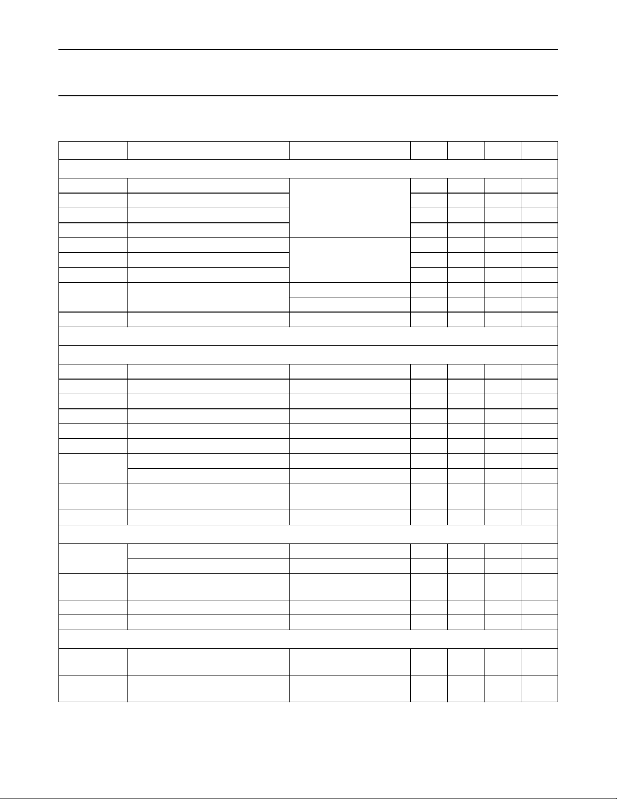
QUICK REFERENCE DATA
SYMBOL PARAMETER CONDITIONS MIN. TYP. MAX. UNIT
V
s1
V
s1
I
s1
I
s1
V
s2
V
s2
I
s2
I
s2
supply voltage 1 (pins 56 and 28) note 1 7 8.5 10 V
operating range 8.1 8.5 8.9 V
supply current 1 FM − 28 − mA
supply current 1 AM − 24 − mA
supply voltage 2 (pin 5) note 1 4.5 5.0 5.5 V
operating range 4.75 5.0 5.25 V
supply current 2 FM − 31 − mA
supply current 2 AM − 28 − mA
S+N/N signal-to-noise AM m = 0.3 − 57 − dB
THD distortion AM − 12%
S+N/N signal-to-noise FM ∆f = 22.5 kHz at pins 43 and 47 66 72 − dB
THD distortion FM ∆f = 75 kHz − 0.1 0.35 %
α channel separation (adjusted) 40 −−dB
T
amb
operating ambient temperature −40 − +85 °C
Note to the quick reference data
1. IC is functional, specified parameters may deviate from limits which are valid for operating range.
September 1993 2

Philips Semiconductors Preliminary specification
ICE car radio TEA6821T
ORDERING INFORMATION
TYPE
NUMBER
TEA6821T VSO56
NAME DESCRIPTION VERSION
PACKAGE
plastic very small outline package; 56 leads
SOT190-1
September 1993 3
Philips Semiconductors Preliminary specification
ICE car radio TEA6821T
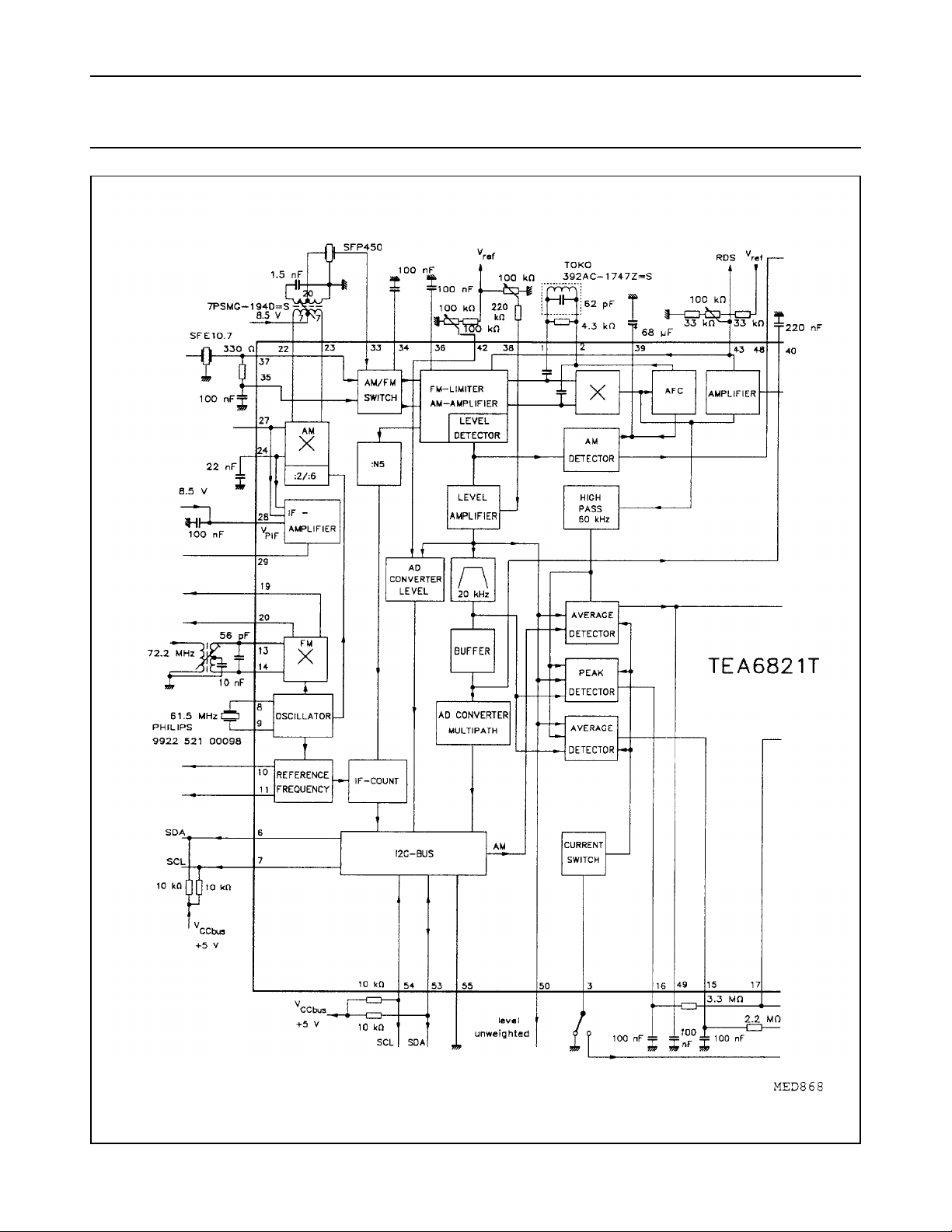
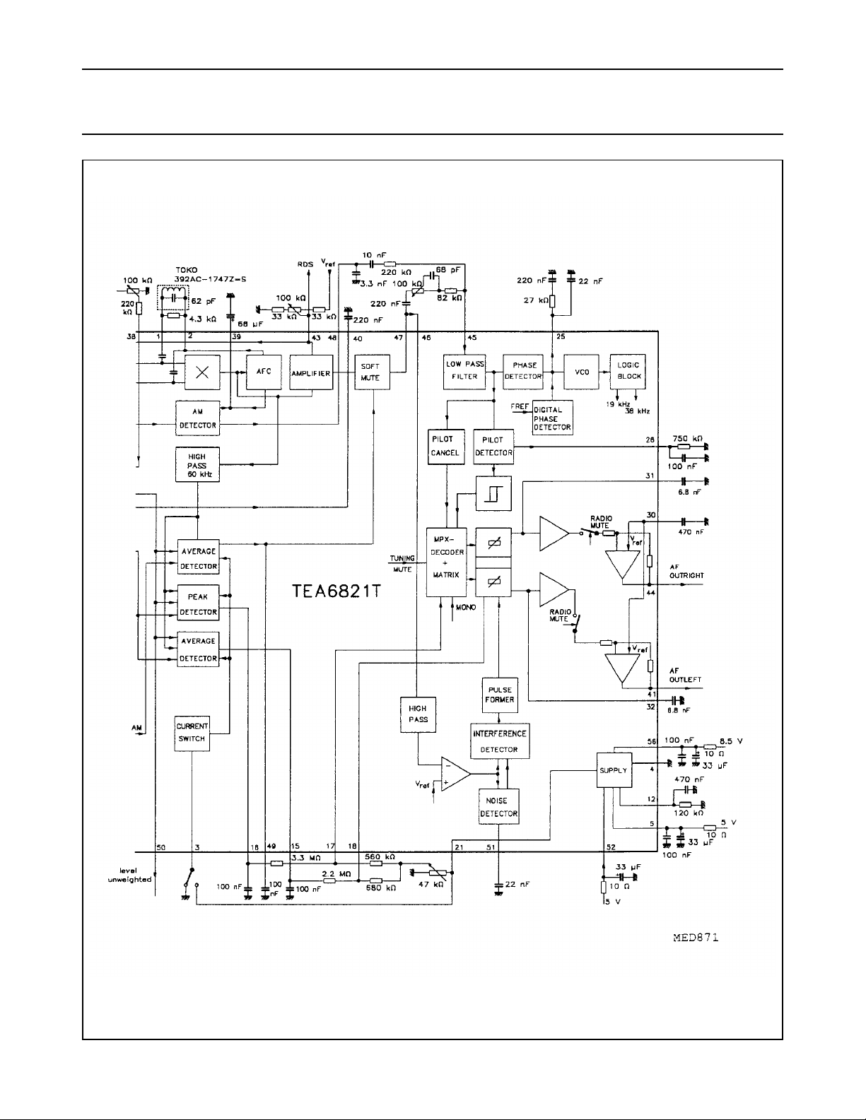
Fig.1 Block diagram (continued in Fig.2).
September 1993 4
Philips Semiconductors Preliminary specification
ICE car radio TEA6821T
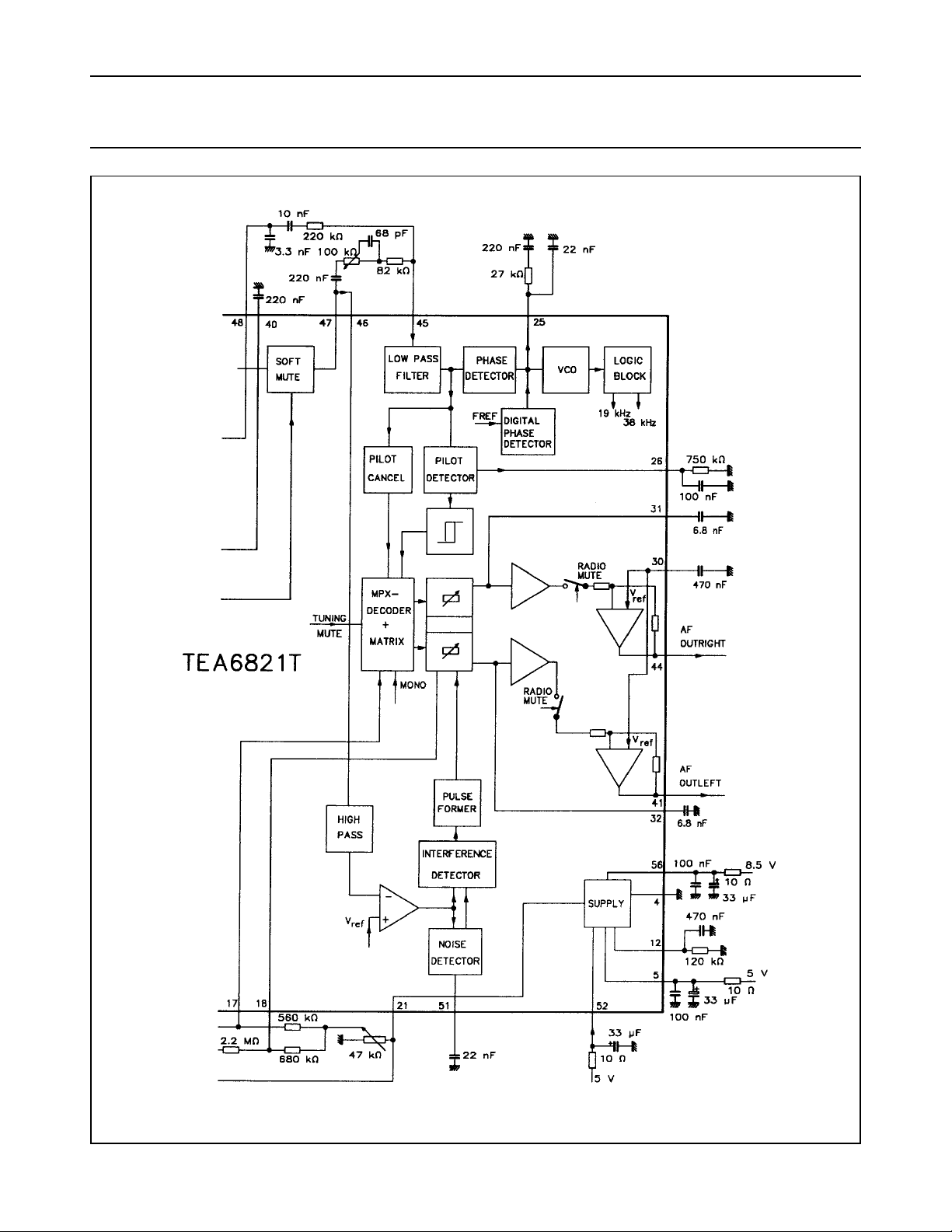
Fig.2 Block diagram (continued from Fig.1).
September 1993 5
Philips Semiconductors Preliminary specification
ICE car radio TEA6821T
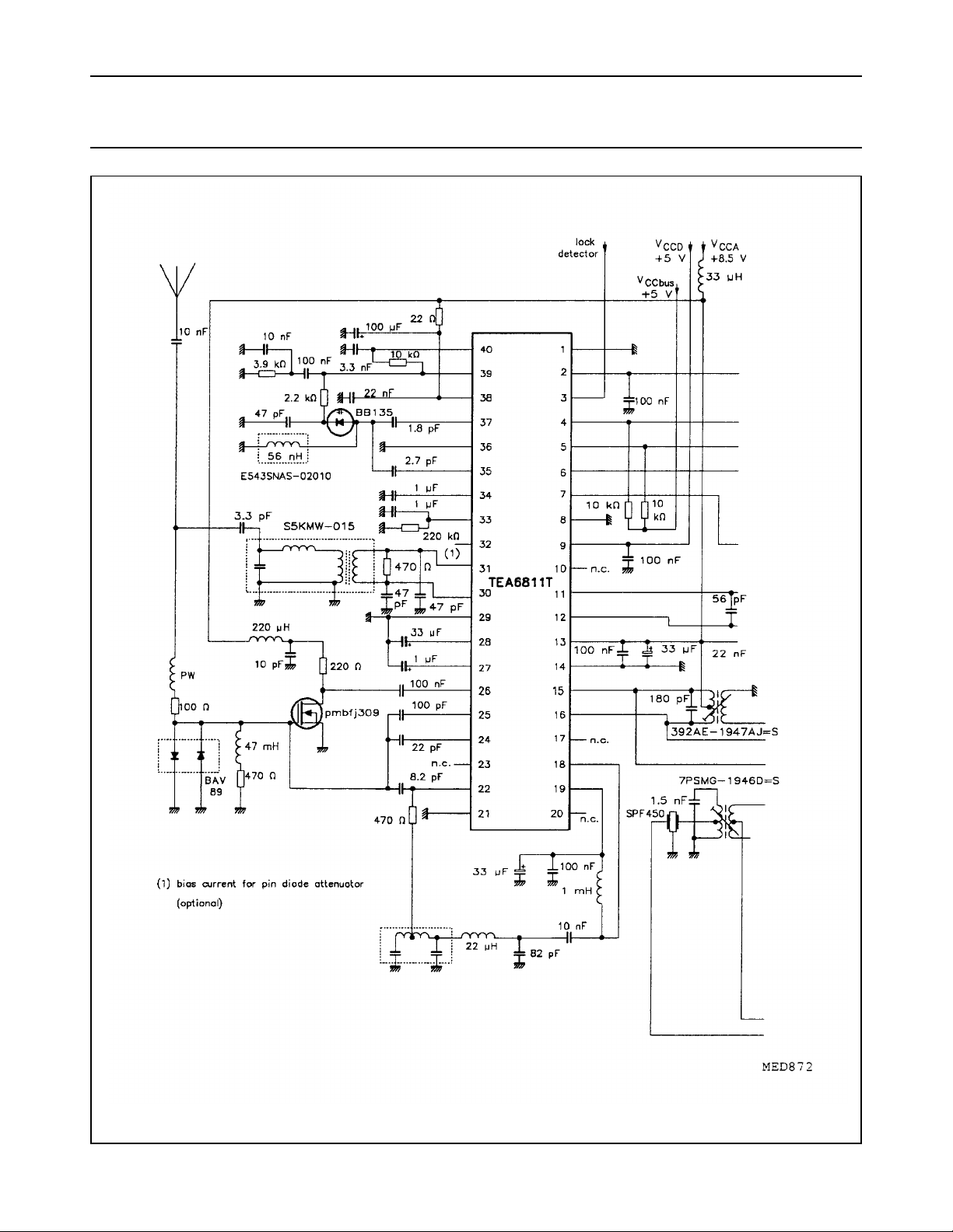
Fig.3 ICE91 application diagram (continued in Fig.4).
September 1993 6
Philips Semiconductors Preliminary specification
ICE car radio TEA6821T
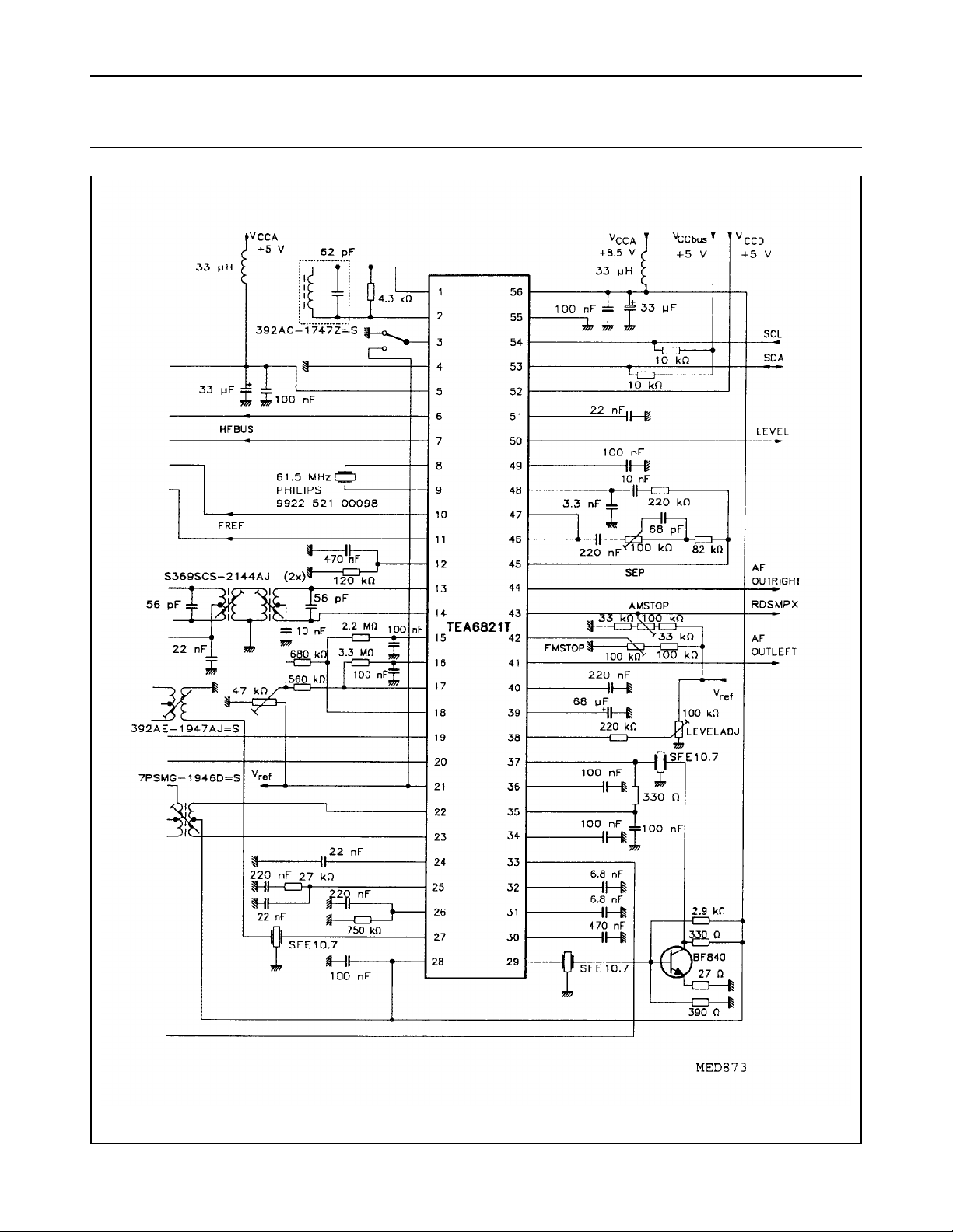
Fig.4 ICE91 application diagram (continued from Fig.3).
September 1993 7
Philips Semiconductors Preliminary specification
ICE car radio TEA6821T
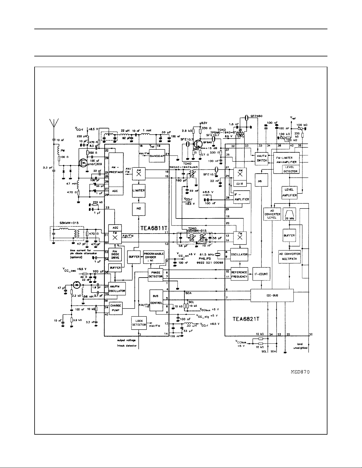
Fig.5 AM/FM car radio receiver with TEA6811T and TEA6821T (continued in Fig.6).
September 1993 8
Philips Semiconductors Preliminary specification
ICE car radio TEA6821T
Fig.6 AM/FM car radio receiver with TEA6811T and TEA6821T (continued from Fig.5).
September 1993 9

Philips Semiconductors Preliminary specification
ICE car radio TEA6821T
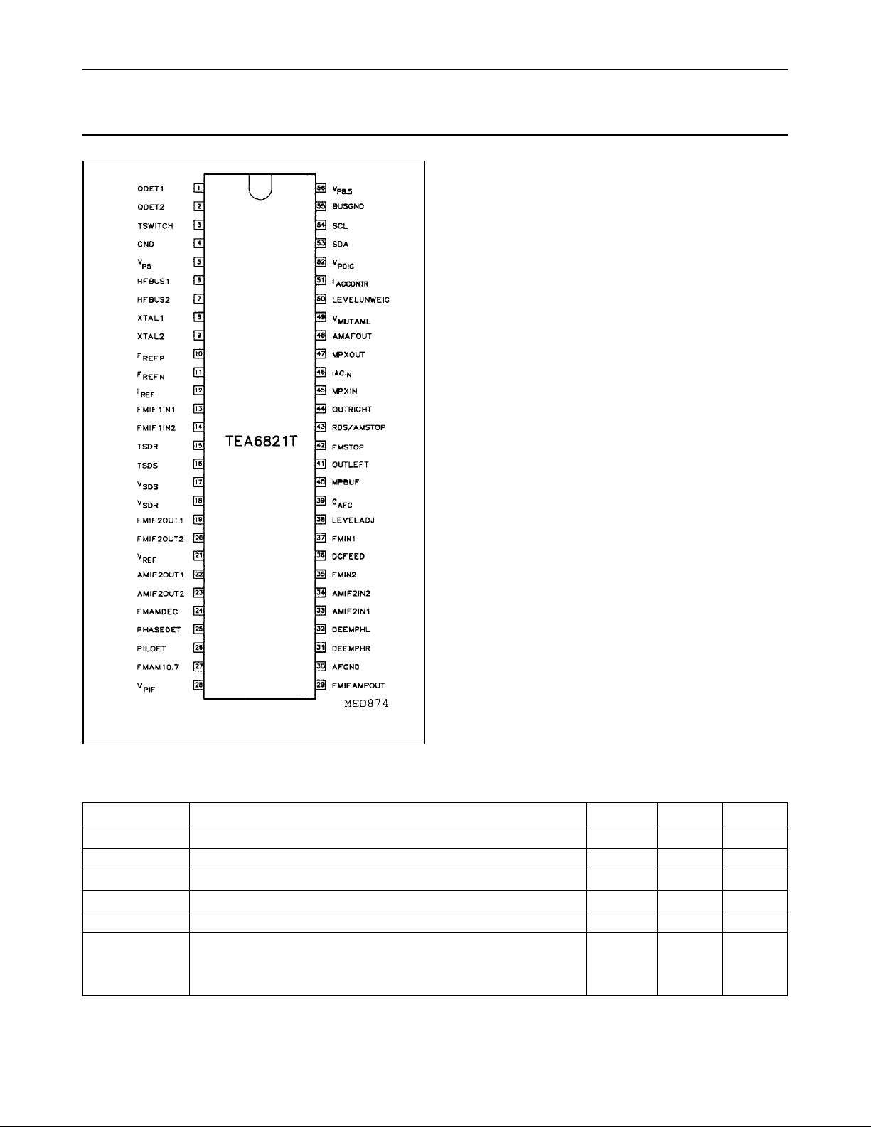
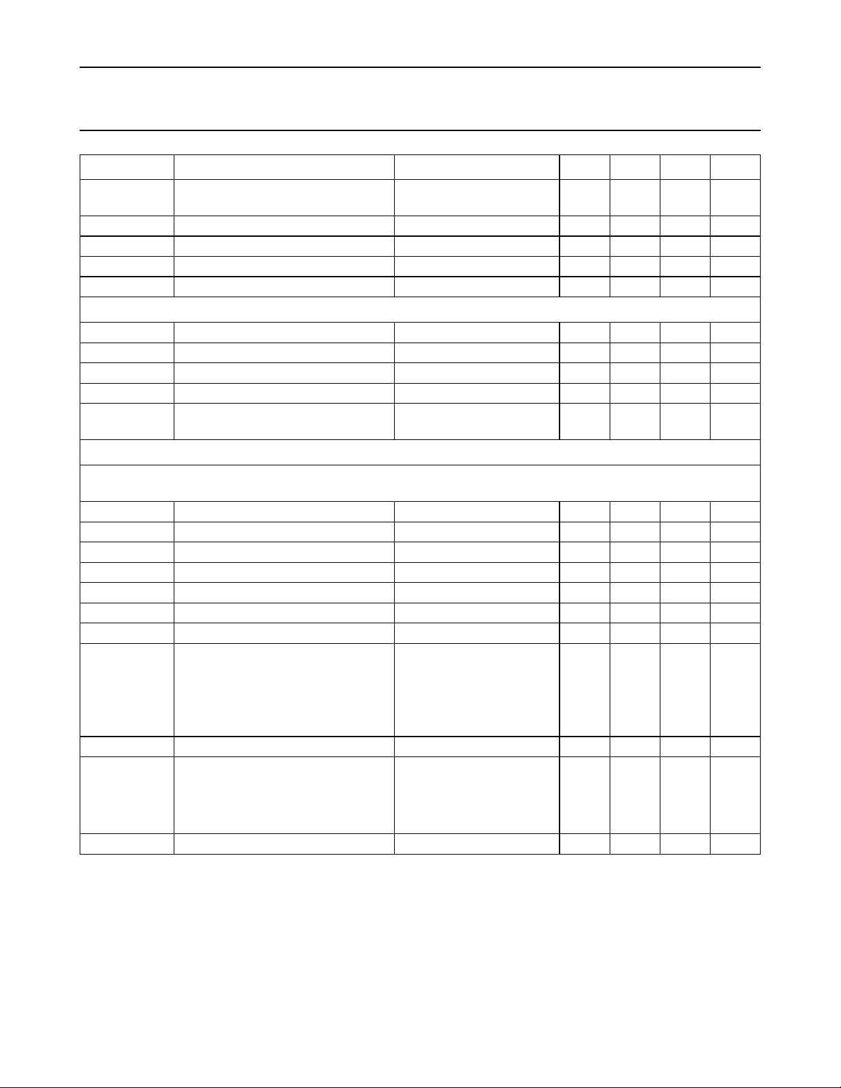
PINNING
SYMBOL PIN DESCRIPTION
QDET1 1 demodulator tank
QDET2 2 demodulator tank
TSWITCH 3 time switch
GND 4 analog ground
V
P5
5 5 V supply voltage
HFBUS1 6 HF bus, pull-up to 5 V
HFBUS2 7 HF bus, pull-up to 5 V
XTAL1 8 crystal oscillator
XTAL2 9 crystal oscillator
F
F
I
REF
REFP
REFN
10 PLL reference frequency
11 PLL reference frequency
12 reference current
FMIF1IN1 13 70 MHz FM-IF input
FMIF1IN2 14 70 MHz FM-IF input
TSDR 15 time constant for SDR
TSDS 16 time constant for SDS
V
V
SDS
SDR
17 SDS control voltage
18 SDR control voltage
FMIF2OUT1 19 FM mixer output
FMIF2OUT2 20 FM mixer output
V
REF
21 reference voltage
AMIF2OUT1 22 AM mixer output
AMIF2OUT2 23 AM mixer output
FMAMDEC 24 FM/AM 10.7 MHz decoupling
PHASEDET 25 phase detector
PILDET 26 pilot detector
FMAM10.7 27 FM/AM 10.7 MHz input
V
PIF
28 VP IF amplifier
SYMBOL PIN DESCRIPTION
FMIFAMPOUT 29 FM-IF amplifier output
AFGND 30 AF ground
DEEMPHR 31 de-emphasis capacitor right
DEEMPHL 32 de-emphasis capacitor left
AMIF2IN1 33 AM IF2 input 1
AMIF2IN2 34 AM IF2 input 2
FMIN2 35 FM limiter input
DCFEED 36 DC feed FM limiter
FMIN1 37 FM limiter input
LEVELADJ 38 level adjust
C
AFC
39 AFC capacitor
MPBUF 40 multipath buffer time constant
OUTLEFT 41 AF output left
FMSTOP 42 FMSTOP adjust
RDS/AMSTOP 43 MPX for RDS/AMSTOP adjust
OUTRIGHT 44 AF output right
MPXIN 45 stereo decoder MPX input
IAC
IN
46 IAC input
MPXOUT 47 FM demodulator MPX output
AMAFOUT 48 AM demodulator AF output
V
MUTAML
49 mute voltage / AM level
LEVELUNWEIG 50 level unweighted
I
ACCONTR
V
PDIG
51 IAC control voltage
52 VP digital
SDA 53 SDA, pull-up to 5 V
SCL 54 SCL, pull-up to 5 V
BUSGND 55 bus ground
V
P8.5
56 VP 8.5 V
September 1993 10
Philips Semiconductors Preliminary specification
ICE car radio TEA6821T
Fig.7 Pin configuration.
LIMITING VALUES
In accordance with the Absolute Maximum Rating System (IEC 134).
SYMBOL PARAMETER MIN. MAX. UNIT
V
V
V
T
T
V
s1
s2
s3
stg
amb
ESD
supply voltage 1 (pins 56 and 28) −0.3 +12 V
supply voltage 2 (pin 5) −0.3 +6.5 V
supply voltage 3 (pin 52) −0.3 +6.5 V
storage temperature −55 +150 °C
operating ambient temperature −40 +85 °C
electrostatic handling (note 1)
for pins 8 and 9 −±100 V
for other pins −±300 V
Note to the limiting values
1. Charge device model class B: discharging a 200 pF capacitor through a 0 Ω series resistor.
September 1993 11
Philips Semiconductors Preliminary specification
ICE car radio TEA6821T
CHARACTERISTICS
V
56-4=V28-4
= 8.5 V, V
SYMBOL PARAMETER CONDITIONS MIN. TYP. MAX. UNIT
Current consumption
I
s1
I
56
I
28
I
+ I
19
20
I
s1
I
56
I
+ I
22
23
I
s2
I
s3
supply current 1 FM 24 30 36 mA
supply current 1at pin 56 16 20 24 mA
supply current 1 at pin 28 2.4 3.0 3.6 mA
supply current 1 at pins 19 and 20 4.8 6.0 7.2 mA
supply current 1 AM 18 24 30 mA
supply current 1at pin 56 9.5 12 15 mA
supply current 1 at pins 22 and 23 8 10 12.5 mA
supply current 2 at pin 5 FM 18 21 25 mA
supply current 3 at pin 52 8 10 12 mA
FM IF path
5-4
= V
52-55
= 5 V, T
= +25 °C unless otherwise specified.
amb
AM 14 17 21 mA
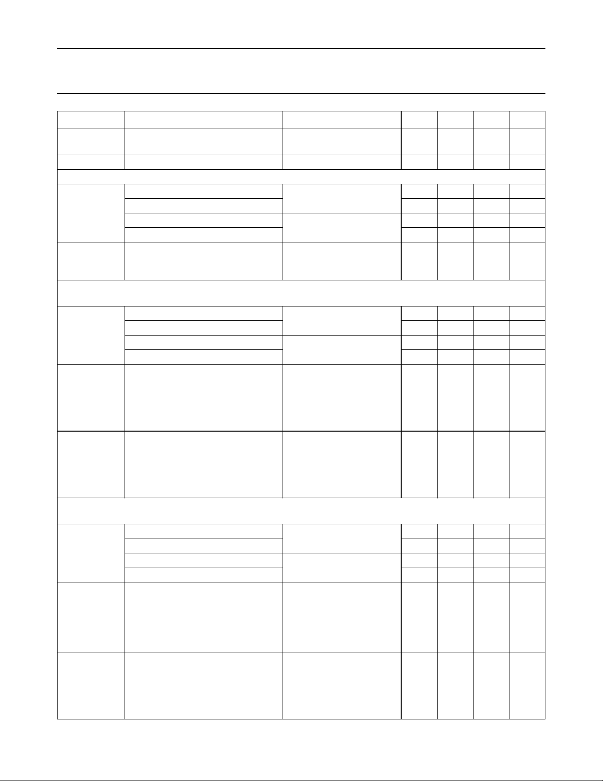
FM mixer
R
13-14
C
13-4,C14-4
R
opt
R
19-20
, C
C
19-4
20-4
I
19IF2/V13-14IF1
I
, I
19
20
input resistance 5 7 − kΩ
input capacitance − 3 4.5 pF
optimum generator resistance − 1.2 − kΩ
output resistance 15 20 − kΩ
output capacitance − 57pF
conversion gain 1.65 1.9 2.2 mS
mixer bias current 2.4 3.0 3.6 mA
mixer leakage current in AM position −−2µA
V
19-20
maximum output voltage
12.0 14.0 − V
(peak-to-peak value)
IP3 third order intermodulation 114 124 − dBµV
Oscillator
f
osc
oscillator frequency − 61.5 − MHz
oscillator spread −−250 Hz
∆f
/∆T temperature dependence of
osc
oscillator frequency
R
1
C
0
crystal motional resistance −−70 Ω
crystal shunt capacitance −−5pF
crystal type PHILIPS
9922 521 00098
− 30 − ppm/K
FM IF2 amplifier
V
29-4/V27-24
amplifier gain loaded with 330 Ω;
8 1012dB
see Fig.9
V
27-24
maximum input voltage for 1 dB
80 110 − mV
compression point (RMS value)
September 1993 12
Philips Semiconductors Preliminary specification
ICE car radio TEA6821T
SYMBOL PARAMETER CONDITIONS MIN. TYP. MAX. UNIT
V
29-4
R
27-24
C
, C
27-4
24-4
R
29-4
C
29-4
FM IF2 limiter
V
1-2/V37-35
C
37-4
R
1-2
C
1-2
V
1-2
maximum output voltage
220 270 − mV
(RMS value)
input resistance 300 330 360 Ω
input capacitance −−5pF
output resistance 300 330 360 Ω
output capacitance −−5pF
limiter gain see Fig.10 − 74 − dB
input capacitance −−5pF
output resistance −−1.0 kΩ
output capacitance 10 15 20 pF
limiter output voltage
500 700 − mV
(peak-to-peak value)
FM demodulator
f
= 1kHz; deviation = 22.5 kHz; Rg= 50 Ω; V
mod
= 10 mV; with de-emphasis = 50 µS; coil quality = 15 unless
37-35
otherwise specified.
V
R
47-4
47out
MPX output (RMS value) 160 200 240 mV
output resistance −−500 Ω
B AF bandwidth 200 −−kHz
V
R
43-4
43out
MPX output for RDS (RMS value) 160 200 240 mV
output resistance −−500 Ω
B AF bandwidth 200 −−kHz
V
V
37-35
37-35
start of limiting (RMS value) αAF = −3 dB − 40 60 µV
input voltage for
signal-plus-noise-to-noise ratio
(RMS value)
see Fig.11 for pin 47
(MPXOUT) and Fig.12 for
pin 43 (RDS/AMSTOP)
S+N/N = 26 dB − 40 55 µV
S+N/N = 46 dB − 100 140 µV
S + N/N signal-plus-noise-to-noise ratio 66 72 − dB
V
43FM/V43AM
suppression ∆f = 22.5 kHz; 55 60 − dB
f
= 1 kHz;
modAM
mAM= 30%;
= 3 mV to 300 mV
V
37-35
V
47FM/V47AM
suppression V
= 1 mV to 300 mV 55 60 − dB
37-35
September 1993 13
Philips Semiconductors Preliminary specification
ICE car radio TEA6821T
SYMBOL PARAMETER CONDITIONS MIN. TYP. MAX. UNIT
THD total harmonic distortion detuning ≤ 50 kHz;
∆f = 75 kHz; f
without de-emphasis
L
= typical value
demod
pin 43 − 0.1 0.35 %
V
= 300 µV to 800 mV
37-35
pin 47 − 0.1 0.35 %
V
= 1 mV to 800 mV
37-35
∆V
43AFCdisabled
/∆V
43AFCactive
demodulator frequency control
(AFC) efficiency at 100 kHz detune
from exact tuning
∆V
43
residual DC-offset ∆L
= typical value;
demod
10 µV<V
80 µV<V
Unweighted level voltage
BW
50
R
out50
V
50-4
V/20 dB slope of level unweighted voltage
/VK temperature dependence V
∆V
50-4
Adjust of level unweighted voltage and V
∆V
50
∆V
/∆V
50-4
R
38
V
38-4
bandwidth 500 −−kHz
output resistance −−100 Ω
level unweighted voltage see Fig.13; V38 = 2.52 V;
V
≤ 2.5 µV 1.8 2.4 3.2 V
37-35
V
= 1.0 mV 2.7 3.4 4.7 V
37-35
V
≤ 100 µV
37-35
∆V
/∆V
50-4
37-35
; typical adjusting range see Figs 14 and 17.
mutaml
adjusting range V
adjusting gain −−0.9 −−
38-4
(RMS) < 300 mV
= 1 mV − 4.0 − mV/VK
37-35
= 1 mV (RMS) −±2−V
37-35
input resistance − 80 − kΩ
internal bias voltage − 2.6 − V
Muting dependence on adjust of level unweighted voltage; typical curve see Fig.15.
α = V
∆α /∆V
43/V47
49
start of mute V49/V21 = 0.6 − 3 −−
mute slope α= −6 dB − 25 − dB/V
Soft mute, time constant control, mono/stereo blend and high-cut control
Time constant control (see application diagram Fig.3): Slow or fast attack and decay time constants for soft mute,
mono/stereo and high-cut control can be chosen connecting pin 3 to GND or pin 21.
Mute voltage: The static mute voltage follows the level unweighted voltage as function of FM IF
adjust voltage V
of Tswitch. Typical curve for mute voltage dependence on V
V
49-4
. It additionally depends on multipath level, noise (adjacent channel interferences) and the position
38-4
see Fig.16.
37-35
mute voltage V38 = 2.52 V;
V
≤ 2.5 µV 1.8 2.2 3.2 V
37-35
= 1.0 mV 2.7 3.3 4.7 V
V
37-35
= 1 kHz
mod
30 34 − dB
<80µV − 100 1000 mV
37-35
< 800 mV − 10 30 mV
37-35
0.75 0.845 0.95 V
voltage and level
2
September 1993 14
Philips Semiconductors Preliminary specification
ICE car radio TEA6821T
SYMBOL PARAMETER CONDITIONS MIN. TYP. MAX. UNIT
V/20 dB slope of mute voltage ∆V
∆V
/VK temperature dependence V
49-4
Attack and decay time for mute voltage.
I
49
charge current pin 3 connected to GND − 3.0 −µA
discharge current −−3.6 −µA
charge current pin 3 connected to pin 21 − 130 −µA
discharge current −−160 −µA
∆f muting activated by 60 kHz
FM interference
Time constant for mono/stereo blend voltage. The mono/stereo blend voltage is generated as a function of FM IF
voltage, multipath level, noise and position of Tswitch.
I
16
charge current V
discharge current pin 3 connected to GND −−18 −µA
charge current V
discharge current pin 3 connected to pin 21 −−800 −µA
m mono/stereo blend activated by
20 kHz AM interference
∆f mono/stereo blend activated by
60 kHz FM interference
Time constant for high-cut control voltage (SDR). The high-cut control voltage is generated as a function of FM IF
voltage, multipath level, noise and position of Tswitch.
I
15
charge current V
discharge current pin 3 connected to GND −−0.44 −µA
charge current V
discharge current pin 3 connected to pin 21 −−44 −µA
m high-cut control activated by 20 kHz
AM interference
∆f high-cut control activated by 60 kHz
FM interference
49-4
/∆V
37-35V37-35
≤ 100 µV
0.75 0.845 0.95 V
(RMS) < 300 mV
= 1 mV − 4.0 − mV/VK
37-35
pin 3 connected to GND;
V
= 3 mV;
37-35
V49 < 2 V; f
= 3 mV; − 0.5 −µA
37-35
= 3 mV; − 26 −µA
37-35
V
< 2 V; V
16
R
> 50 MΩ;
L16
= 20 kHz; pin 3
f
mod
= 60 kHz
mod
37-35
= 3 mV;
− 30 − kHz
− 45 − %
connected to GND
pin 3 connected to pin 21 − 40 − %
V
< 3 V; V
16
R
> 50 MΩ;
L16
f
= 60 kHz; pin 3
mod
37-35
= 3 mV;
− 30 − kHz
connected to GND
pin 3 connected to pin 21 − 22 − kHz
= 3 mV; − 0.4 −µA
37-35
= 3 mV; − 41 −µA
37-35
V
R
f
mod
15
L15
< 2 V; V
> 50 MΩ;
= 20 kHz;
37-35
= 3 mV;
pin 3 connected to GND − 40 − %
pin 3 connected to pin 21 − 35 − %
V
R
f
mod
15
L15
< 2 V; V
> 50 MΩ;
= 60 kHz;
37-35
= 3 mV;
pin 3 connected to GND − 25 − kHz
pin 3 connected to pin 21 − 20 − kHz
2
2
September 1993 15
 Loading...