

Philips TEA6822T, TEA6820T Datasheet

INTEGRATED CIRCUITS
DATA SH EET
TEA6820T; TEA6822T
In Car Entertainment (ICE) car
radio
Preliminary specification
Supersedes data of 1996 Oct 18
File under Integrated Circuits, IC01
1997 Feb 12
Philips Semiconductors Preliminary specification
In Car Entertainment (ICE) car radio TEA6820T; TEA6822T
FEATURES
General
• FM mixer for conversion from FM-IF
FM-IF2= 10.7 MHz
• AM mixer for conversion from AM-IF1= 10.7 MHz to
AM-IF2= 450 kHz
• FM-IF gain stage
• Crystal oscillator providing mixer frequencies and
references for IF-count and stereo decoder
• FM quadrature demodulator with automatic centre
frequency adjustment and THD compensation
• Level, multi-path and noise detectors
• Soft mute
• Stereo noise cancelling and variable de-emphasis
• PLL stereo decoder
• Noise blanker
• AM IF-amplifier and demodulator
• I2C-bus transceiver with interface to enable direct data
transfer to radio front-end
• IF-count for AM and FM
• Reference frequency generation for PLL synthesizer.
ORDERING INFORMATION
= 72.2 MHz to
1
Stereo decoder
• Adjustment-free PLL VCO
• Pilot depending mono/stereo switching
• Analog control of mono/stereo blend
• Adjacent channel noise suppression (114 kHz)
• Pilot cancelled
• Analog control of de-emphasis
• Integrated low-pass filters for 190 kHz adjacent channel
interferences and signal delay for interference
absorption circuit.
GENERAL DESCRIPTION
The TEA6820T together with the TEA6810T and the
TEA6822T together with the TEA6811T forms an AM/FM
electronic tuned car radio in a double conversion receiver
concept.
TYPE NUMBER
NAME DESCRIPTION VERSION
TEA6820T VSO56 plastic very small outline package; 56 leads; face down SOT190-2
TEA6822T VSO56 plastic very small outline package; 56 leads SOT190-1
PACKAGE
1997 Feb 12 2

Philips Semiconductors Preliminary specification
In Car Entertainment (ICE) car radio TEA6820T; TEA6822T
QUICK REFERENCE DATA
SYMBOL PARAMETER CONDITIONS MIN. TYP. MAX. UNIT
V
DDA1
I
DDA1
I
19+I20
I
22+I23
V
DDA2
I
DDA2
V
DDA3
I
DDA3
V
DDD
I
DDD
SN+
-------------N
THD total harmonic distortion FM mode; ∆f=75kHz − 0.1 0.35 %
α
cs
T
amb
analog supply voltage 1 (+5 V; pin 5) note 1 4.5 5.0 5.5 V
operating range 4.75 5.0 5.25 V
analog supply current 1 (pin 5) FM mode 17 21 25 mA
AM mode 14 17 21 mA
total FM mixer output current 4.8 6.0 7.2 mA
total AM mixer output current 10 12 14 mA
analog supply voltage 2 (pin 28) note 1 7.0 8.5 10 V
operating range 8.1 8.5 8.9 V
analog supply current 2 (pin 28) FM mode 2.4 3.0 3.6 mA
analog supply voltage 3 (+8.5 V; pin 56) note 1 7.0 8.5 10 V
operating range 8.1 8.5 8.9 V
analog supply current 3 (pin 56) FM mode 19 24 28 mA
AM mode 9.5 12 15 mA
digital supply voltage 1 (+5 V; pin 5) note 1 4.5 5.0 5.5 V
operating range 4.75 5.0 5.25 V
digital supply current (pin 52) note 1 8 10 12 mA
signal plus noise-to-noise ratio FM mode;
66 75 − dB
∆f = 22.5 kHz at
pins 43 and 47
AM mode; m = 0.3 54 60 − dB
AM mode − 1.5 3 %
channel separation (adjusted) 40 −−dB
operating ambient temperature −40 − +85 °C
Note
1. IC is operating; specified parameters may deviate from limits which are valid for operating range.
1997 Feb 12 3
Philips Semiconductors Preliminary specification
In Car Entertainment (ICE) car radio TEA6820T; TEA6822T
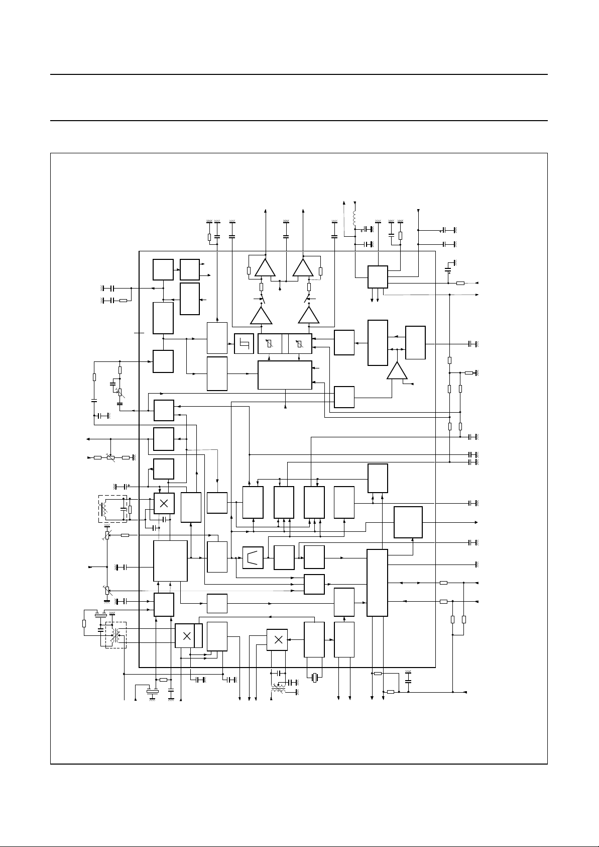
BLOCK DIAGRAM
CC
+8.5 V
+8.5 V
, full pagewidth
1 kΩ
220 kΩ
68 pF
10 nF
3.3 nF
RDS
33 kΩ
ref
V
AMSTOP
TOKO
P392BC-1977Z
LEVELADJ
ref
V
FMSTOP
SFP450
1.5 nF
TOKO
22 nF220 nF
82 kΩ
220 nF
100 kΩ
L13
62 pF
R40 R51
100 kΩ
R39
100 kΩ
TR5
7PSAG-1946D = S
27 kΩ
100 kΩ
82 kΩ
V
i.c.
R41
33 kΩ
68 µF
100 nF
100
CC1
25
46
45
47
43 48
39
2
4.3 kΩ
1
42 38
nF
34
33
22 23
SFE10.7
10.7 MHz
VCO
PHASE
LOW
PASS
SOFT
MPX
AFC
FM-LIMITER
AM/FM
373635
330 Ω
LOGIC
BLOCK
PHASE
DIGITAL
DETECTOR
DETECTOR
FILTER
MUTE
BUFFER
AM
DELOG
LEVEL
DETECTOR
AM-AMPLIFIER
SWITCH
AM
27
24
100 nF
10.7 MHz
820 kΩ
38 kHz
19 kHz
ref
f
PILOT
PILOT
TEA6820T
TEA6822T
PASS
HIGH
AMPLIFIER
LEVEL
:N5
IF-
÷ 2 /÷ 6
22 nF
6.8 nF
100 nF
31
26
DETECTOR
CANCELLER
60 kHz
AMPLIFIER
AMPLIFIER
29
28
100 nF
radio
mute
AVERAGE
19
10.7 MHz
10.7 MHz
OUTRIGHT
44
-
+
MPX-
DETECTOR
20 kHz
FM
13
20
56 pF
72.2 MHz
470 nF
30
int1
V
AND
DECODER
tuning
mute
PEAK
DETECTOR
BUFFER
14
10
41
+
MATRIX
nF
OUTLEFT
6.8 nF
-
radio
mute
mono
AVERAGE
DETECTOR
ADC
PATH
MULTI-
ADC
LEVEL
OSCILLATOR
9
8
61.5 MHz
PHILIPS
9922 521 00098
V
22 µH
100
56
32
PULSE
FORMER
HIGH
PASS
FILTER
PEAK
DETECTOR
IF-
COUNTER
FREQUENCY
REFERENCE
11
10
ref
f
or Daiwa AT - 49
47 µF
nF
4
SUPPLY
int2
int1
V
V
DETECTOR
INTERFERENCE
SWITCH
CURRENT
C-BUS
2
I
6
10 kΩ
SCL
SDA
470 nF
-
AM
7
10 kΩ
CCAN
V
120 kΩ
12
NOISE
DETECTOR
+
int2
V
TURE
SATION
COMPEN-
TEMPERA-
100 nF
+5 V
5
47 µF
nF
100
33 µF
52
21
51
12 kΩ
1 MΩ
17 18
3.3 MΩ
15
16
3
50 49
40
55
Ω
330
53
Ω
330
54
10 kΩ
MHA253
10 Ω
CCDIG
+5 V
V
ref
V
100 nF
33 kΩ
1.2 MΩ
100 nF
2.2 MΩ
nF
100
100 nF
10 kΩ
220 nF
220 nF
DDD
V
level
SDASCL
+5 V
Fig.1 Block diagram.
1997 Feb 12 4
Philips Semiconductors Preliminary specification
In Car Entertainment (ICE) car radio TEA6820T; TEA6822T
PINNING
SYMBOL PIN DESCRIPTION
QDET1 1 demodulator tank 1
QDET2 2 demodulator tank 2
TSWITCH 3 time switch input
AGND 4 analog ground
V
DDA1
5 analog supply voltage 1 (+5 V)
HFBUS1 6 HF bus 1 output;
pull-up to +5 V
HFBUS2 7 HF bus 2 output;
pull-up to +5 V
XTAL1 8 crystal oscillator1
XTAL2 9 crystal oscillator2
f
ref(p)
10 PLL reference frequency
output (p)
f
ref(n)
11 PLL reference frequency
output (n)
I
ref
12 reference current
FMIF1IN1 13 72 MHz FM-IF input 1
FMIF1IN2 14 72 MHz FM-IF input 2
TSDR 15 time constant for SDR
TSDS 16 time constant for SDS
V
V
SDS
SDR
17 SDS control voltage input
18 SDR control voltage input
FMIF2OUT1 19 FM mixer output 1
FMIF2OUT2 20 FM mixer output 2
V
ref
21 reference voltage output
AMIF2OUT1 22 AM mixer output 1
AMIF2OUT2 23 AM mixer output 2
FMAMDEC 24 FM/AM 10.7 MHz decoupling
PHASEDET 25 phase detector output
PILDET 26 pilot detector output
FMAM10.7 27 FM/AM 10.7 MHz input
V
DDA2
28 analog supply voltage 2
SYMBOL PIN DESCRIPTION
FMIFAMPOUT 29 FM-IF amplifier output
AFGND 30 AF ground
DEEMPHR 31 de-emphasis capacitor right
DEEMPHL 32 de-emphasis capacitor left
AMIF2IN1 33 AM-IF
AMIF2IN2 34 AM-IF
input 1
2
input 2
2
FMIN2 35 FM limiter input
DCFEED 36 DC feed FM limiter
FMIN1 37 FM limiter input
LEVELADJ 38 level adjustment input
C
AFC
39 AFC capacitor
MPBUF 40 multi-path buffer time constant
OUTLEFT 41 AF output left
FMSTOP 42 FMSTOP adjustment input
RDS/AMSTOP 43 MPX for RDS/AMSTOP
adjustment input
OUTRIGHT 44 AF output right
MPXIN 45 stereo decoder MPX input
i.c. 46 internally connected
MPXOUT 47 FM demodulator MPX output
AMAFOUT 48 AM demodulator AF output
V
mute/AML
49 mute voltage/AM level
LEVELUNWEIG 50 unweighted level output
IAC
V
DDD
CONTR
51 IAC control voltage
52 digital supply voltage
SDA 53 serial data input/output;
pull-up to +5 V
SCL 54 serial clock input;
pull-up to +5 V
DGND 55 digital ground
V
DDA3
56 analog supply voltage 3
(+8.5 V)
1997 Feb 12 5
Philips Semiconductors Preliminary specification
In Car Entertainment (ICE) car radio TEA6820T; TEA6822T
handbook, halfpage
TSWITCH
HFBUS1
HFBUS2
FMIF1IN1
FMIF1IN2
FMIF2OUT1
FMIF2OUT2
AMIF2OUT1
AMIF2OUT2
FMAMDEC
PHASEDET
FMAM10.7
QDET1
QDET2
AGND
V
DDA1
XTAL1
XTAL2
f
ref(p)
f
ref(n)
I
ref
TSDR
TSDS
V
SDS
V
SDR
V
ref
PILDET
V
DDA2
1
2
3
4
5
6
7
8
9
10
11
12
13
14
15
16
17
18
19
20
21
22
23
24
25
26
27
28
TEA6822T
MHA204
56
V
DDA3
55
DGND
54
SCL
53
SDA
52
V
DDD
51
IAC
50
LEVELUNWEIG
49
V
mute/AML
48
AMAFOUT
47
MPXOUT
46
i.c.
45
MPXIN
44
OUTRIGHT
43
RDS/AMSTOP
42
FMSTOP
41
OUTLEFT
40
MPBUF
39
C
AFC
38
LEVELADJ
37
FMIN1
36
DCFEED
35
FMIN2
34
AMIF2IN2
33
AMIF2IN1
32
DEEMPHL
31
DEEMPHR
30
AFGND
29
FMIFAMPOUT
CONTR
handbook, halfpage
IAC
LEVELUNWEIG
V
mute/AML
AMAFOUT
OUTRIGHT
RDS/AMSTOP
OUTLEFT
LEVELADJ
AMIF2IN2
AMIF2IN1
DEEMPHL
DEEMPHR
FMIFAMPOUT
V
DDA3
DGND
SCL
SDA
V
DDD
CONTR
MPXOUT
i.c.
MPXIN
FMSTOP
MPBUF
C
AFC
FMIN1
DCFEED
FMIN2
AFGND
56
55
54
53
52
51
50
49
48
47
46
45
44
43
TEA6820T
42
41
40
39
38
37
36
35
34
33
32
31
30
29
MHA419
1
QDET1
2
QDET2
3
TSWITCH
4
AGND
5
V
DDA1
6
HFBUS1
7
HFBUS2
8
XTAL1
9
XTAL2
10
f
ref(p)
11
f
ref(n)
12
I
ref
13
FMIF1IN1
14
FMIF1IN2
15
TSDR
16
TSDS
17
V
SDS
18
V
SDR
FMIF2OUT1
19
FMIF2OUT2
20
V
21
ref
AMIF2OUT1
22
AMIF2OUT2
23
FMAMDEC
24
PHASEDET
25
PILDET
26
FMAM10.7
27
V
28
DDA2
Fig.2 Pin configuration for TEA6822T.
FUNCTIONAL DESCRIPTION
Stereo decoder
By changing the value of the input resistor at pin 12 the
MPX input can be adapted to the level of the FM
demodulator output (see Fig.16).
1997 Feb 12 6
Fig.3 Pin configuration for TEA6820T (top view).
A 3rd order low-pass filter (f
= 90 kHz) at the MPX input
g
provides an extra 190 kHz ACI suppression.
An interference gate is connected at the MPX demodulator
outputs. For AM the VCO is switched off.
Philips Semiconductors Preliminary specification
In Car Entertainment (ICE) car radio TEA6820T; TEA6822T
LIMITING VALUES
In accordance with the Absolute Maximum Rating System (IEC 134).
SYMBOL PARAMETER CONDITIONS MIN. MAX. UNIT
V
DDA1
V
DDA2
V
DDA3
V
DDD
T
stg
T
amb
V
es
Note
1. Charge device model class B: equivalent to discharging a 200 pF capacitor via a 0 Ω series resistor.
analog supply voltage 1 (pin 5) −0.3 +6.5 V
analog supply voltage 2 (pin 28) −0.3 +12 V
analog supply voltage 3 (pin 56) −0.3 +12 V
digital supply voltage (pin 52) −0.3 +6.5 V
storage temperature −55 +150 °C
operating ambient temperature −40 +85 °C
electrostatic handling note 1
pins 8 and 9 −100 +100 V
all other pins −300 +300 V
CHARACTERISTICS
V
56-4=V28-4
= 8.5 V; V
5-4=V52-55
=5V; T
amb
=25°C; f
= 1 kHz; deviation = 22.5 kHz; Rg=50Ω; V
mod
37-35
=10mV;
with de-emphasis = 50 µs; coil quality = 15; unless otherwise specified.
SYMBOL PARAMETER CONDITIONS MIN. TYP. MAX. UNIT
Current consumption
I
DDA1
analog supply current 1 (pin 5) FM mode 17 21 25 mA
AM mode 14 17 21 mA
I
DDA2
I
DDA3
analog supply current 2 (pin 28) FM mode 2.4 3.0 3.6 mA
analog supply current 3 (pin 56) FM mode 19 24 28 mA
AM mode 9.5 12 15 mA
I
DDD
I
19+I20
I
22+I23
digital supply current (pin 52) 8 10 12 mA
total FM mixer output current 4.8 6.0 7.2 mA
total AM mixer output current AM mode 10 12 14 mA
FM-IF path; see Fig.4
V
19-20 max(p-p)
maximum output voltage
12.0 14.0 − V
(peak-to-peak value)
; I
I
19
20
mixer bias current 2.4 3.0 3.6 mA
mixer leakage current in AM position −− 2µA
I
19IF2/V13-14IF1
R
i
C
i
R
opt
R
o
C
o
conversion gain 1.65 1.9 2.2 mS
input resistance (pins 13 to 14) 5 7 − kΩ
input capacitance (pins 13 to 14) − 3 4.5 pF
optimum generator resistance − 1.2 − kΩ
output resistance (pins 19 to 20) 15 20 − kΩ
output capacitance (pins 19 to 4
− 12 14 pF
and pins 20 to 4)
IP3 third order intermodulation 114 124 − dBµV
1997 Feb 12 7
Philips Semiconductors Preliminary specification
In Car Entertainment (ICE) car radio TEA6820T; TEA6822T
SYMBOL PARAMETER CONDITIONS MIN. TYP. MAX. UNIT
Oscillator
f
osc
∆f
osc
/∆T temperature dependence of
∆f
osc
R
1
C
0
FM-IF
amplifier
2
V
27-24 max(rms)
V
29-4 max(rms)
V
29-4/V27-24
∆V
29-4/V27-24
R
i
C
i
R
o
C
o
FM-IF
limiter
2
V
o 1-2(p-p)
V
1-2/V37-35
C
i
R
o
C
o
oscillator frequency − 61.5 − MHz
oscillator frequency spread −− 250 Hz
−1
oscillator frequency
crystal type PHILIPS
9922 521 00098
− 30 × 10−6− K
crystal motional resistance −− 70 Ω
crystal shunt capacitance −− 5pF
maximum input voltage for 1 dB
80 110 − mV
compression point (RMS value)
maximum output voltage
220 320 − mV
(RMS value)
amplifier gain loaded with 330 Ω;
912 15dB
see Fig.5
gain temperature dependence −25 °C<T
+50 °C<T
< +50 °C − 0.1 − dB/K
amb
< +75 °C0 −−dB/K
amb
input resistance (pins 27 to 24) 300 330 360 Ω
input capacitance (pins 27 to 4) −− 5pF
output resistance (pin 29) 300 330 360 Ω
output capacitance (pins 29 to 4) −− 5pF
limiter output voltage
500 700 − mV
(peak-to-peak value)
limiter gain see Fig.6 − 80 − dB
input capacitance (pins 37 to 4) −− 5pF
output resistance (pins 1 to 2) −− 1.0 kΩ
output capacitance (pins 1 to 2) 10 15 20 pF
1997 Feb 12 8

Philips Semiconductors Preliminary specification
In Car Entertainment (ICE) car radio TEA6820T; TEA6822T
SYMBOL PARAMETER CONDITIONS MIN. TYP. MAX. UNIT
FM demodulator
V
47-4(rms)
V
43-4(rms)
V
37-35(rms)
V
37-35(rms)
∆V
43DC
V
43FM/V43AM
V
47FM/V47AM
∆V
43-44AFCdis
/∆V
43-44AFCactive
R
o
SN+
-------------N
THD total harmonic distortion detuning ≤50 kHz;
MPX output voltage (RMS value) 160 200 240 mV
MPX output voltage for RDS
160 200 240 mV
(RMS value)
start of limiting voltage
αAF= −3dB − 25 40 µV
(RMS value)
input voltage for signal plus
noise-to-noise ratio (RMS value)
see Fig.7 for pin 47
(MPXOUT) and Fig.8 for
pin 43 (RDS/AMSTOP)
− 30 45 µV
− 70 100 µV
50 60 − dB
residual DC-offset voltage ∆L
SN+
-------------N
SN+
-------------N
demod
26 dB=
46 dB=
= typical value
10 µV<V
80 µV<V
AM suppression ∆f= 22.5 kHz;
f
= 1 kHz;
modAM
<80µV − 100 1000 mV
37-35
< 800 mV − 10 30 mV
37-35
mAM= 30%;
V
= 3 to 300 mV
37-35
AM suppression V
demodulator frequency control
= 1 to 300 mV 50 60 − dB
37-35
28 32 − dB
voltage (AFC) efficiency at
100 kHz detune from exact tuning
output resistance (pin 47) −− 3kΩ
output resistance (pin 43) −− 1.5 kΩ
AF bandwidth (pin 43) 200 −−kHz
signal plus noise-to-noise ratio 66 75 − dB
∆f = 75 kHz; f
mod
= 1 kHz
without de-emphasis;
L
= typical value
demod
pin 43;
V
37-35
= 300 µV
− 0.1 0.35 %
to 800 mV
pin 47;
V
37-35
= 1 to 800 mV
− 0.1 0.35 %
1997 Feb 12 9
Philips Semiconductors Preliminary specification
In Car Entertainment (ICE) car radio TEA6820T; TEA6822T
SYMBOL PARAMETER CONDITIONS MIN. TYP. MAX. UNIT
Unweighted voltage level
V
50-4
/∆V
∆V
50-4
37-35
/VK temperature dependence V
∆V
50-4
I
50(max)source
I
50(max)sink
R
o50
ADJUSTMENT OF UNWEIGHTED VOLTAGE LEVEL AND V
∆V
50
V
38-4
/∆V
∆V
50-4
38-4
R
i38
MUTING DEPENDENCE ON ADJUST OF LEVEL UNWEIGHTED VOLTAGE; note 2
α =V
43/V47
∆α/∆V
49
Soft mute, time constant control, mono/stereo blend and high-cut control; see Fig.22
unweighted voltage level see Fig.9; V38= 2.52 V
≤ 2.5 µV 1.6 2.2 3.0 V
V
37-35
= 1.0 mV 2.7 3.4 4.7 V
V
37-35
slope of unweighted voltage level 100 µV (RMS) ≤ V
37-35
< 300 mV
temperature
0.75 0.9 1.05 V/20 dB
compensation off
temperature
0.6 0.75 0.9 V/20 dB
compensation on
=1mV
37-35
temperature
− 5.0 − mV/VK
compensation off
temperature
− 2.0 − mV/VK
compensation on
maximum output source current 0.3 −−mA
maximum output sink current −50 −−µA
output resistance −− 300 Ω
mute/AML
adjusting range voltage V
; note 1
= 10 mV (RMS) −1.8 − +1.8 V
37-35
internal bias voltage − 2.6 − V
adjusting gain −−0.9 −−
input resistance − 80 − kΩ
start of mute V49/V21= 0.625 1 3 7 dB
mute slope α = −6dB − 25 − dB/V
M
UTE VOLTAGE; note 3
V
∆V
49-4
49-4
/∆V
37-35
mute voltage V38= 2.52 V
V
37-35
V
37-35
slope of mute voltage 100 µV (RMS) ≤ V
< 300 mV
/VK temperature dependence V
∆V
49-4
37-35
1997 Feb 12 10
< 2.5 µV 1.8 2.2 3.2 V
= 1.0 mV 2.7 3.4 4.7 V
37-35
0.75 0.9 1.05 V/20 dB
=1mV − 5.0 − mV/VK

Philips Semiconductors Preliminary specification
In Car Entertainment (ICE) car radio TEA6820T; TEA6822T
SYMBOL PARAMETER CONDITIONS MIN. TYP. MAX. UNIT
ATTACK AND DECAY TIME FOR MUTE VOLTAGE
I
49
∆f muting activated by 60 kHz FM
V
43/V47
T
IME CONSTANT FOR MONO/STEREO BLEND VOLTAGE; note 4
I
16
m mono/stereo blend activated by
∆f mono/stereo blend activated by
charge current pin 3 connected to GND − 3.5 −µA
discharge current pin 3 connected to GND −−4.0 −µA
charge current pin 3 connected to pin 5 − 150 −µA
discharge current pin 3 connected to pin 5 −−170 −µA
interference
maximum mute depth by 60 kHz
FM interference
charge current V
<3V; V
V
49
f
= 60 kHz
mod
pin 3 connected to GND;
V
43/V47
pin 3 connected to pin 5;
V
43/V47
pin 3 connected to GND − 15 − dB
pin 3 connected to pin 5 − 10 − dB
= 3 mV;
37-35
37-35
=9dB
=6dB
=3mV;
− 40 − kHz
− 40 − kHz
− 0.6 −µA
pin 3 connected to GND
discharge current V
37-35
= 3 mV;
−−17 −µA
pin 3 connected to GND
charge current V
37-35
= 3 mV;
− 23 −µA
pin 3 connected to pin 5
discharge current V
37-35
= 3 mV;
−−750 −µA
pin 3 connected to pin 5
20 kHz AM interference
V
R
f
16
L16
mod
<2V; V
>50MΩ;
= 20 kHz;
37-35
=3mV;
data byte 2 bit 5 = 0
pin 3 connected to GND − 45 − %
pin 3 connected to pin 5 − 45 − %
data byte 2 bit 5 = 1
pin 3 connected to GND − 55 − %
pin 3 connected to pin 5 − 55 − %
60 kHz FM interference
V
R
f
16
L16
mod
<2V; V
>50MΩ;
= 60 kHz
37-35
=3mV;
pin 3 connected to GND − 50 − kHz
pin 3 connected to pin 5 − 50 − kHz
1997 Feb 12 11
Philips Semiconductors Preliminary specification
In Car Entertainment (ICE) car radio TEA6820T; TEA6822T
SYMBOL PARAMETER CONDITIONS MIN. TYP. MAX. UNIT
TIME CONSTANT FOR HIGH-CUT CONTROL VOLTAGE SDR; note 5
I
15
charge current V
discharge current V
charge current V
discharge current V
m high-cut control activated by
20 kHz AM interference
∆f high-cut control activated by
60 kHz FM interference
ULTI-PATH DETECTOR
M
f
MP
multi-path detector band-pass
centre frequency
B
MP
band-pass bandwidth 7.0 −−kHz
Reference voltage
V
∆V
I
21
21-4
21-4
output voltage I21= −1 mA 4.5 5.1 5.7 V
temperature dependence − 3.3 − mV/VK
output current −− 1mA
AM-IF path; see Fig.14 and notes 6 and 7
V
22-23 max(p-p)
maximum output voltage
(peak-to-peak value)
, I
I
22
23
mixer bias current 5.0 6.0 7.0 mA
mixer leakage current in FM position −− 2µA
I
22IF2/V27-24IF1
R
27-24
C
27-24
R
22-23
C
22-23
conversion gain 2.2 2.7 3.4 mS
input resistance 300 330 360 Ω
input capacitance − 58pF
output resistance 10.0 20.0 − kΩ
output capacitance − 510pF
IP3 third order intermodulation − 137 − dBµV
37-35
= 3 mV;
− 0.6 −µA
pin 3 connected to GND
37-35
= 3 mV;
−−0.7 −µA
pin 3 connected to GND
37-35
= 3 mV;
− 41 −µA
pin 3 connected to pin 5
37-35
= 3 mV;
−−44 −µA
pin 3 connected to pin 5
V
R
f
15
L15
mod
<2V; V
>50MΩ;
= 20 kHz
37-35
=3mV;
pin 3 connected to GND − 45 − %
pin 3 connected to pin 5 − 45 − %
V
R
f
15
L15
mod
<2V; V
>50MΩ;
= 60 kHz
37-35
=3mV;
pin 3 connected to GND − 50 − kHz
pin 3 connected to pin 5 − 50 − kHz
− 20 − kHz
12 15 − V
1997 Feb 12 12

Philips Semiconductors Preliminary specification
In Car Entertainment (ICE) car radio TEA6820T; TEA6822T
SYMBOL PARAMETER CONDITIONS MIN. TYP. MAX. UNIT
DETECTOR; notes 8 and 9
AM
V
48-4(rms)
V
33-34(rms)
AF output level (RMS value) R
sensitivity voltage (RMS value) − 50 75 µV
AM-IF
minimum input voltage
2
(RMS value)
AM-IF
maximum input voltage
2
(RMS value)
R
33-34
C
24-23
R
o48
C
o48
SN+
-------------N
IF2 input resistance 1.8 2.0 2.2 kΩ
IF2 input capacitance − 10 15 pF
output resistance 27 33 39 kΩ
output capacitance −− 10 pF
signal plus noise-to-noise ratio 54 60 − dB
THD total harmonic distortion m = 0.8;
Notes to the characteristics
1. For typical adjusting range see Figs 10 and 13.
2. For typical curve see Fig.11.
3. The static mute voltage follows the unweighted voltage level as function of FM-IF2 voltage and level adjustment
voltage V
. It additionally depends on multi-path level, noise (adjacent channel interferences) and the position of
38-4
TSWITCH (pin 3). For typical curve for mute voltage dependence see Fig.12.
4. The mono/stereo blend voltage is generated as a function of FM-IF2 voltage, multi-path level, noise and position of
TSWITCH.
5. The high-cut control voltage is generated as a function of FM-IF2 voltage, multi-path level, noise and position of
TSWITCH.
6. f
= 10.7 MHz; f
IF1
= 450 kHz for AM mixer.
IF2
7. The AM oscillator signal is generated by division of the 61.5 MHz crystal oscillator. Two divider ratios programmable
by the I2C-bus: divide by 6 (AM-IF1= 10.7 MHz); divide by 2 (AM-IF1= 30 MHz).
8. For typical AM level curve see Fig.15.
9. For AM detector; f
AMIF2
= 450 kHz; f
= 400 Hz; m = 30%.
mod
> 500 kΩ;
L48
100 µV ≤ V
SN+
-------------N
SN+
-------------N
26 dB=
46 dB=
33-34
≤ 300 mV
190 240 290 mV
− 200 400 µV
THD ≤ 5%; m = 0.8 −− 100 µV
THD ≤ 5%; m = 0.8 800 −−mV
− 1.5 3.0 %
300 µV ≤ V
33-34
≤ 200 mV
1997 Feb 12 13
Philips Semiconductors Preliminary specification
In Car Entertainment (ICE) car radio TEA6820T; TEA6822T
STEREO DECODER CHARACTERISTICS
Input signal (∆f = 75 kHz) V
MPX(p-p)
nominal input resistor (pin 45) Ri= 168 kΩ; T
SYMBOL PARAMETER CONDITIONS MIN. TYP. MAX. UNIT
V
44-4(rms)
V
41-4(rms)
; V
V
44-4
; I
I
44(max)
V
44-4/V41-4
; R
R
o44
R
Lmin
α
cs
SN+
-------------N
;
41-4
41(max)
o41
AF output voltage (RMS value) 800 900 1000 mV
DC output voltage 3.1 3.6 4.1 V
maximum output current 150 −−µA
difference of output voltage −1 − +1 dB
output resistor −−600 Ω
minimum load resistor 12 −−kΩ
channel separation (adjusted) 40 −−dB
signal plus noise-to-noise ratio f = 20 Hz to 15 kHz 74 80 − dB
THD total harmonic distortion − 0.1 0.3 %
MPX input overdrive margin THD = 1% 4 −−dB
= 1.7 V; modulation frequency f
=25°C; unless otherwise specified.
amb
= 1 kHz; de-emphasis time constant t = 50 µs;
mod
Carrier and harmonic suppression at the output; note 1
α
19
α
38
α
57
α
76
α
2
α
3
α
57
α
67
pilot signal f = 19 kHz − 50 − dB
subcarrier f = 38 kHz − 50 − dB
f = 57 kHz − 50 − dB
f = 76 kHz − 60 − dB
intermodulation f
mod
f
mod
traffic radio (ARI) f = 57 kHz − 70 − dB
subsidiary communications
f = 67 kHz 70 −−dB
authorization
α
114
α
190
RR ripple rejection at output f
adjacent channel frequency f = 114 kHz − 80 − dB
f = 190 kHz − 70 − dB
= 100 Hz; Vr= 100 mV
r
Mono/stereo control
V
i(pil)
pilot threshold voltage stereo on − 24 30 mV
mono on 8 20 − mV
∆V
i(pil)
switch hysteresis V
ion/Vioff
External mono/stereo control; note 2
− 0.765V21control voltage channel separation see Fig.17
V
17
α =6dB −−110 − mV
α =16dB −−40 − mV
= 10 kHz; f
= 13 kHz; f
= 1 kHz − 60 − dB
spur
= 1 kHz − 58 − dB
spur
− 30 − dB
eff
− 2 − dB
1997 Feb 12 14
Philips Semiconductors Preliminary specification
In Car Entertainment (ICE) car radio TEA6820T; TEA6822T
SYMBOL PARAMETER CONDITIONS MIN. TYP. MAX. UNIT
Muting functions (mute via I2C-bus)
, ∆V
∆V
44
41
α
mute
High-cut control; see Fig.18
− 0.765V21control voltage note 3
V
18
t
de-emph
Voltage controlled oscillator; note 4
f
osc
Noise blanker
DC offset voltage tune mute −50 − +50 mV
radio mute (in combination
−400 − +400 mV
with tune mute)
tune mute 60 −−dB
radio mute (in combination with
80 −−dB
tune mute)
t
de-emph
t
de-emph
=50µs0−−mV
=80µs −300 −−mV
control range of de-emphasis 50 − 80 µs
oscillator frequency range 225 228 231 kHz
NTERFERENCE DETECTION FULLY INTERNAL FROM LEVEL DETECTOR
I
t
sup
interference suppression time 40 50 −µs
TRIGGER THRESHOLD CONTROL
I
51 charge
I
51 discharge
charge current (into +4 V) − 45 −µA
discharge current (from +8.5 V) −−900 −µA
TRIGGER SENSITIVITY MEASUREMENT WITH PULSED MODULATION OF FM-IF2; see Figs 19 and 20
V
37-35(p)
V
51
∆V
51
I
offset
trigger sensitivity for test signal 1
(peak value)
trigger sensitivity for test signal 2
(peak value)
trigger threshold variation with
frequency modulation of FM-IF
and f
= 15 kHz (pin 51)
mod
gate input offset current at pins 31
V38= 2.52 V; note 5 −−0.8 mV
= 2.52 V; note 6 100 −−mV
V
38
= 2.52 V; note 6 5.0 −−mV
V
38
= 2.52 V; note 6 100 −−mV
V
38
V
= 100 mV; ∆f=0kHz − 6.4 − V
37-35
2
V
= 100 mV; ∆f=75kHz − 520 − mV
37-35
− 20 50 nA
and 32 during suppression pulse
duration
1997 Feb 12 15
 Loading...