

Philips TEA1210TS Datasheet

INTEGRATED CIRCUITS
DATA SH EET
TEA1210TS
Highefficiency,highcurrentDC/DC
converter
Product specification
Supersedes data of 1999 Mar 08
File under Integrated Circuits, IC03
2000 Nov 28

Philips Semiconductors Product specification
High efficiency, high current DC/DC converter TEA1210TS
FEATURES
• Fully integrated DC/DC converter circuit, featuring
internal very low R
• Up-or-down conversion
• Start-up from 1.85 V input voltage
• Adjustable output voltage
• High efficiency over large load range
• 600 kHz switching frequency
• Low quiescent power consumption
• Synchronizing with external clock
• Two selectable current limits for efficient battery use in
case of dynamic loads
• Up to 100% duty cycle in down mode
• Undervoltage lockout
• Shut-down function
• 16-pin small body SSOP16 package.
APPLICATIONS
• Cellularphones,Personal Digital Assistants(PDAs) and
others
• Supply voltage source for low-voltage chip sets
• Portable computers
• Battery backup supplies.
power MOSFETs
DSon
GENERAL DESCRIPTION
The TEA1210TS is a fully integrated DC/DC converter.
Efficient, compact and dynamic power conversion is
achieved using a novel digitally controlled concept like
Pulse Width Modulation (PWM) or Pulse Frequency
Modulation (PFM), integrated low R CMOS power
switches with low parasitic capacitances, and fully
synchronous rectification.
The device operates at 600 kHz switching frequency
which enables the use of external components with
minimum size. The switching frequency can be locked to
an external high-frequency clock.
Optionally, the device can be kept in the Pulse Width
Modulation (PWM) mode regardless of the load applied.
Deadlock is prevented by an on-chip undervoltage lockout
circuit.
Twoselectablecurrent limits inupconversionmodeenable
efficient battery use even at highly dynamic loads such as
cellular phone electronics.
ORDERING INFORMATION
TYPE NUMBER
NAME DESCRIPTION VERSION
TEA1210TS SSOP16 plastic shrink small outline package; 16 leads; body width 4.4 mm SOT369-1
2000 Nov 28 2
PACKAGE

Philips Semiconductors Product specification
High efficiency, high current DC/DC converter TEA1210TS
QUICK REFERENCE DATA
T
= −40 to +80 °C; all voltages measured with respect to ground; positive currents flow into the IC; unless otherwise
amb
specified.
SYMBOL PARAMETER CONDITIONS MIN. TYP. MAX. UNIT
Voltage levels
PCONVERSION; PIN U/D = LOW
U
V
I
V
O
V
I(start)
V
I(uvlo)
OWNCONVERSION; PIN U/D = HIGH
D
V
I
V
O
input voltage V
output voltage 2.90 − 5.50 V
start-up input voltage IL< 200 mA 1.20 1.60 1.85 V
undervoltage lockout input voltage 1.50 2.10 2.70 V
input voltage 2.90 − 5.50 V
output voltage 1.30 − 5.50 V
GENERAL
V
∆V
fb
window
feedback input voltage 1.20 1.25 1.30 V
output voltage window PWM mode 1.5 2.0 3.0 %
Current levels
I
q
I
shdwn
∆I
lim(up)
I
lim(down)
I
LX
quiescent current on pins LX VI=2.40 V; VO= 3.60 V 100 125 150 µA
current in shut-down mode − 210µA
current limit deviation in up mode I
current limit in down mode 4.8 A
maximum continuous current on
pins LX
Power MOSFETs
R
DSon(N)
drain-to-source on-state resistance
NFET
R
DSon(P)
drain-to-source on-state resistance
PFET
Efficiency
η efficiency upconversion V
Timing
f
sw
f
sync
t
res
switching frequency PWM mode 480 600 720 kHz
synchronization clock input frequency 9 13 20 MHz
response time from standby to P
set to 2.0 A −12 − +12 %
lim(up)
T
=60°C −−1.8 A
amb
Tj=27°C − 56 63 mΩ
Tj=27°C − 68 77 mΩ
= 2.4 V; VO= 3.6 V;
I
T
=20°C
amb
I
=1mA 83 86 − %
L
I
= 100 mA 90 93 − %
L
I
= 500 mA 92 94 − %
L
I
= 1.5 A; not continual 84 86 − %
L
o(max)
− 25 −µs
− 5.50 V
I(start)
2000 Nov 28 3
This text is here in white to force landscape pages to be rotated correctly when browsing through the pdf in the Acrobat reader.This text is here in
_white to force landscape pages to be rotated correctly when browsing through the pdf in the Acrobat reader.This text is here inThis text is here in
white to force landscape pages to be rotated correctly whenbrowsing through the pdf in the Acrobat reader. white to force landscape pages to be ...
2000 Nov 28 4
handbook, full pagewidth
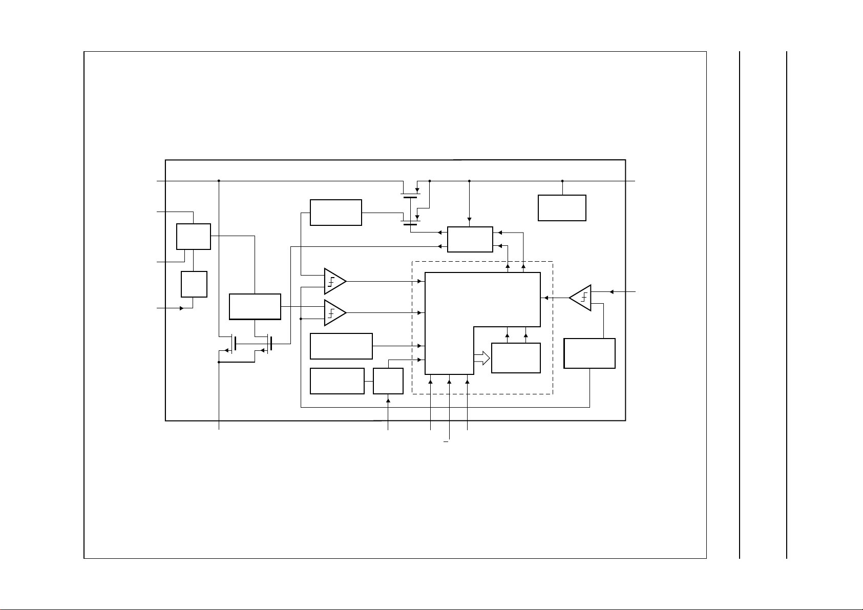
BLOCK DIAGRAM
Philips Semiconductors Product specification
High efficiency, high current DC/DC converter TEA1210TS
LX
ILIMH
ILIML
ILIMSEL
4, 5, 12, 13
7
SWITCH
10
LPF
11
N-type
POWER
FET
GND
I/V
CONVERTER
sense
FET
I/V
CONVERTER
CURRENT LIMIT
COMPARATORS
TEMPERATURE
PROTECTION
13 MHz
OSCILLATOR
P-type POWER FET
sense FET
SYNC
GATE
28, 9 3
SYNC
SHDWN
START-UP
CIRCUIT
CONTROL LOGIC
AND
MODE GEARBOX
DIGITAL CONTROLLER
146
PWM
U/D
TIME
COUNTER
INTERNAL
SUPPLY
TEA1210TS
BAND GAP
REFERENCE
1, 16
15
MGR725
UPOUT
FB
Fig.1 Block diagram.
Philips Semiconductors Product specification
High efficiency, high current DC/DC converter TEA1210TS
PINNING
SYMBOL PIN DESCRIPTION
UPOUT 1, 16 output voltage in up mode;
input voltage in down mode
SYNC 2 synchronization clock input
SHDWN 3 shut-down input
LX 4, 5, 12, 13 inductor connection
U/D 6 up-or-down mode selection
input; active LOW for up mode
ILIMH 7 current limiting resistor 1
connection
GND 8, 9 ground
ILIML 10 current limiting resistor 2
connection
ILIMSEL 11 current limiting selection input
PWM 14 PWM-only mode selection
input
FB 15 feedback input
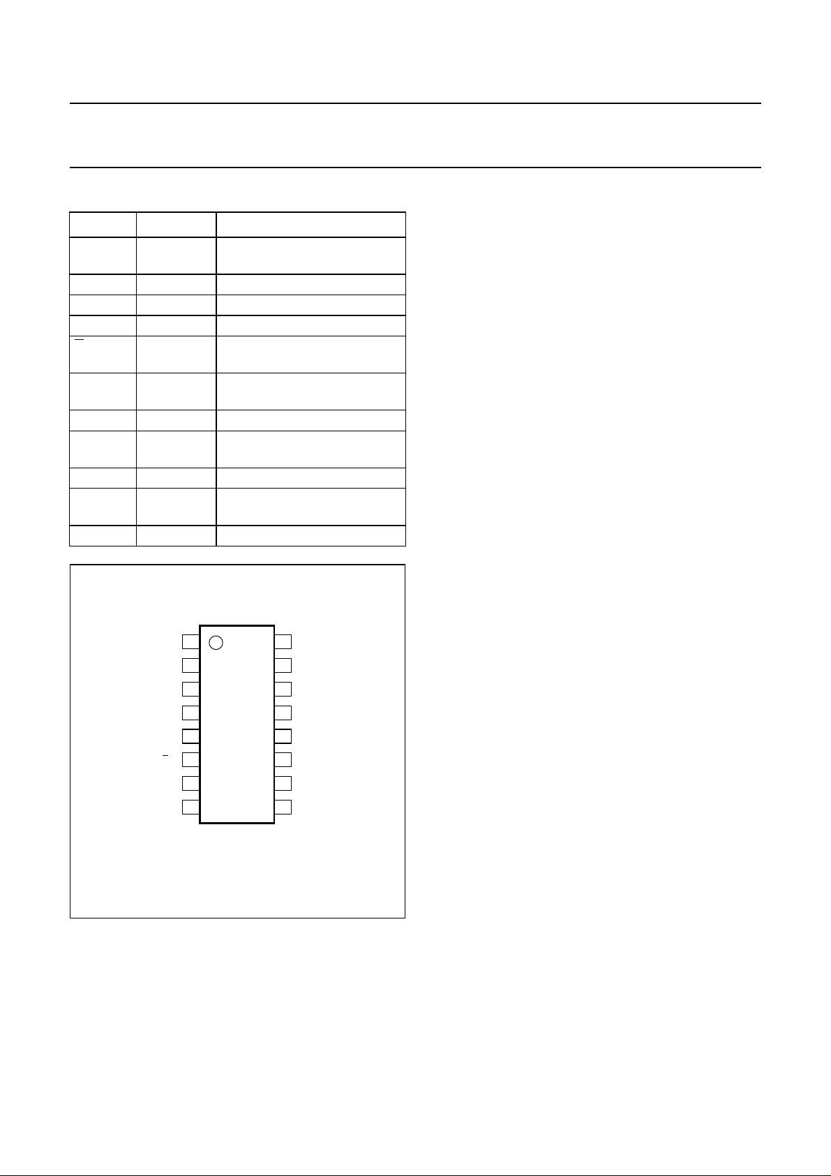
handbook, halfpage
UPOUT
SYNC
SHDWN
LX
LX
U/D
ILIMH
GND
1
2
3
4
TEA1210TS
5
6
7
8
MGR726
16
15
14
13
12
11
10
9
UPOUT
FB
PWM
LX
LX
ILIMSEL
ILIML
GND
Fig.2 Pin configuration.
For all possible applications, the following groups of pins
must be connected together:
• Pins 4, 5, 12 and 13 (pins LX)
• Pins 1 and 16 (pins UPOUT)
• Pins 8 and 9 (pins GND).
FUNCTIONAL DESCRIPTION
Control mechanism
The TEA1210TS DC/DC converter is able to operate in
PFM (discontinuous conduction) or PWM (continuous
conduction) operating mode. All switching actions are
completely determined by a digital control circuit which
usesthe output voltagelevelas itscontrolinput. This novel
digital approachenables the use of a new pulse widthand
frequency modulation scheme, which ensures optimum
power efficiency over the complete operating range of the
converter.
When high output power is requested, the device will
operate in PWM (continuousconduction) operating mode.
This results in minimum AC currents in the circuit
components and hence optimum efficiency, cost and
EMC. In thisoperating mode,the outputvoltage is allowed
to vary between two predefined voltage levels. As long as
the output voltage stays within this so-called window,
switching continues in a fixed pattern. When the output
voltage reaches one of the window borders, the digital
controller immediately reacts by adjusting the pulse width
and inserting a current step in such a way that the output
voltage stays within the window with higher or lower
current capability. This approach enables very fast
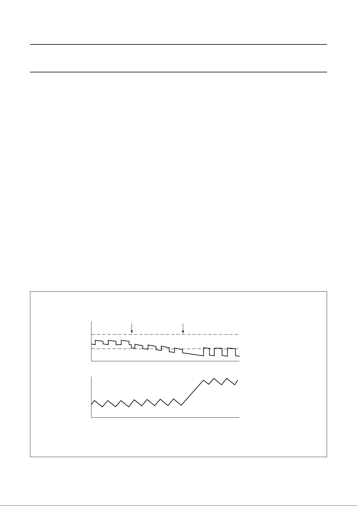
reaction to load variations. Figure 3 shows theconverter’s
response to a sudden load increase. The upper trace
shows the outputvoltage. Theripple ontop ofthe DC level
is a result of the current in the output capacitor, which
changes in sign twice per cycle, times the capacitor’s
internal Equivalent Series Resistance (ESR). After each
ramp-down of the inductor current, i.e. when the ESR
effect increases the output voltage, the converter
determines what to do in the next cycle. As soon as more
load current is taken from the output the output voltage
starts to decay.
When theoutput voltage becomes lower than the low limit
of the window, acorrective action is taken bya ramp-up of
theinductor currentduring a muchlonger time. Asa result,
the DC current levelis increasedand normal PWM control
can continue. The output voltage (including ESR effect) is
again within the predefined window.
Figure 4 depicts the spread of the output voltage window.
Theabsolutevalue is mostdependenton spread, whilethe
actualwindow sizeis not affected. For onespecific device,
the output voltage will not vary more than 2% typically.
In lowoutput power situations,the TEA1210TS willswitch
overto PFM (discontinuousconduction)operating mode in
case the PWM-only mode is not active.
2000 Nov 28 5
Philips Semiconductors Product specification
High efficiency, high current DC/DC converter TEA1210TS
Inthe PFMmode,regulation informationfromearlier PWM
operating modesis used. Thisresults in optimuminductor
peak current levels in the PFM mode, which are slightly
larger than the inductor ripple current in the PWM mode.
As a result,the transitionbetween PFMand PWMmode is
optimum under all circumstances. In the PFM mode,
TEA1210TS regulates the output voltage to the high
window limit shown in Fig.3.
Synchronous rectification
For optimum efficiency over the whole load range,
synchronous rectifiers inside the TEA1210TS ensure that
during the whole second switching phase, all inductor
current will flow through the low-ohmic power MOSFETs.
Special circuitry isincluded whichdetects thatthe inductor
current reaches zero. Following this detection, the digital
controller switches off the power MOSFET and proceeds
regulation.
PWM-only mode
When pin PWM is pulled to HIGH-level in the
upconversion mode, the TEA1210TS will use PWM
regulation independent ofthe loadapplied. Asa result, the
switching frequency does not vary over the whole load
range. Furthermore,the P-type power MOSFET is always
on when the input voltage exceeds the target output
voltage. The internal synchronous rectifier still takes care
that the inductor current does not fall below zero. In this
way, the achieved efficiency is higher than in standard
PWM-controlled converters.
Start-up
Start-up from low input voltage in boost mode is realized
by an independent start-up oscillator, which starts
switching the N-type power MOSFET as soon as the
voltage on pins UPOUT is measured to be sufficiently
high. The switch actions of the start-up oscillator will
increase the output voltage.As soonas theoutput voltage
is high enough for normal regulation, the digital control
system takes over the control of the power MOSFETs.
Undervoltage lockout
As a result of too high load or disconnection of the input
power source, the output voltage can drop so low that
normal regulation cannot be guaranteed. In that case, the
device switches back to start-up mode. If the output
voltage drops down even further, switching is stopped
completely.
Shut-down
When the shut-down input is made HIGH, the converter
disablesboth switchesand power consumptionis reduced
to a few microamperes.
handbook, full pagewidth
load increase
V
o
I
L
start corrective action
Fig.3 Response to load increase.
2000 Nov 28 6
time
time
high window limit
low window limit
MGK925
 Loading...