

Philips TEA1207T Datasheet

INTEGRATED CIRCUITS
DATA SH EET
TEA1207T
High efficiency DC/DC converter
Product specification
Supersedes data of 1999 Oct 21
File under Integrated Circuits, IC03
2000 Nov 27

Philips Semiconductors Product specification
High efficiency DC/DC converter TEA1207T
FEATURES
• Fully integrated DC/DC converter circuit
• Up-or-down conversion
• Start-up from 1.85 V input voltage
• Adjustable output voltage
• High efficiency over large load range
• Power handling capability up to 0.85 A continuous
average current
• 275 kHz switching frequency
• Low quiescent power consumption
• Synchronizing with external clock
• True current limit for Li-ion battery compatibility
• Up to 100% duty cycle in down mode
• Undervoltage lockout
• Shut-down function
• 8-pin SO package.
APPLICATIONS
• Cellular and cordless phones, Personal Digital
Assistants (PDAs) and others
• Supply voltage source for low-voltage chip sets
• Portable computers
• Battery backup supplies
• Cameras.
GENERAL DESCRIPTION
The TEA1207T is a fully integrated DC/DC converter.
Efficient, compact and dynamic power conversion is
achieved using a novel digitally controlled concept like
Pulse Width Modulation (PWM) or Pulse Frequency
Modulation (PFM), integrated low R
switches with low parasitic capacitances, and fully
synchronous rectification.
The device operates at 275 kHz switching frequency
which enables the use of external components with
minimum size. Deadlock is prevented by an on-chip
undervoltage lockout circuit.
Efficient behaviour during short load peaks and
compatibility with Li-ion batteries is guaranteed by an
accurate current limiting function.
CMOS power
DSon
ORDERING INFORMATION
TYPE NUMBER
NAME DESCRIPTION VERSION
TEA1207T SO8 plastic small outline package; 8 leads; body width 3.9 mm SOT96-1
PACKAGE
2000 Nov 27 2

Philips Semiconductors Product specification
High efficiency DC/DC converter TEA1207T
QUICK REFERENCE DATA
SYMBOL PARAMETER CONDITIONS MIN. TYP. MAX. UNIT
Voltage levels
UPCONVERSION; pin U/D = LOW
V
I
V
O
V
I(start)
input voltage V
output voltage 2.80 − 5.50 V
start-up input voltage IL< 125 mA 1.40 1.60 1.85 V
DOWNCONVERSION; pin U/D = HIGH
V
I
V
O
ENERAL
G
V
fb
input voltage 2.80 − 5.50 V
output voltage 1.30 − 5.50 V
feedback voltage 1.19 1.24 1.29 V
Current levels
I
q
I
shdwn
I
LX
∆I
lim
quiescent current on pin 3 down mode; VI=3.6V526572µA
current in shut-down state − 210µA
maximum continuous current on pin 4 T
current limit deviation I
Power MOSFETs
R
DSon
drain-to-source on-state resistance
N-type 0.10 0.20 0.30 Ω
P-type 0.10 0.22 0.35 Ω
Efficiency
η
1
η
2
efficiency upconversion VI= 3.6 V; VO= 4.6 V;
efficiency downconversion VI= 3.6 V; VO= 2.0 V;
Timing
f
sw
f
sync
t
res
switching frequency PWM mode 220 275 330 kHz
synchronization clock input frequency 4 6.5 20 MHz
response time from standby to P
I(start)
=80°C −−0.60 A
amb
= 0.5 to 5 A
lim
up mode −17.5 − +17.5 %
down mode −17.5 − +17.5 %
L1 = 10 µH
=1mA − 88 − %
I
L
I
= 200 mA − 95 − %
L
I
= 1 A; pulsed − 83 − %
L
L1 = 10 µH
=1mA − 86 − %
I
L
I
= 200 mA − 93 − %
L
I
= 1 A; pulsed − 81 − %
L
− 50 −µs
0(max)
− 5.50 V
2000 Nov 27 3
This text is here in white to force landscape pages to be rotated correctly when browsing through the pdf in the Acrobat reader.This text is here in
a
_white to force landscape pages to be rotated correctly when browsing through the pdf in theAcrobatreader.This text is here inThis text is here in
white to force landscape pages to be rotated correctly when browsing through the pdf in the Acrobat reader. white to force landscape pages to be ...
2000 Nov 27 4
ndbook, full pagewidth
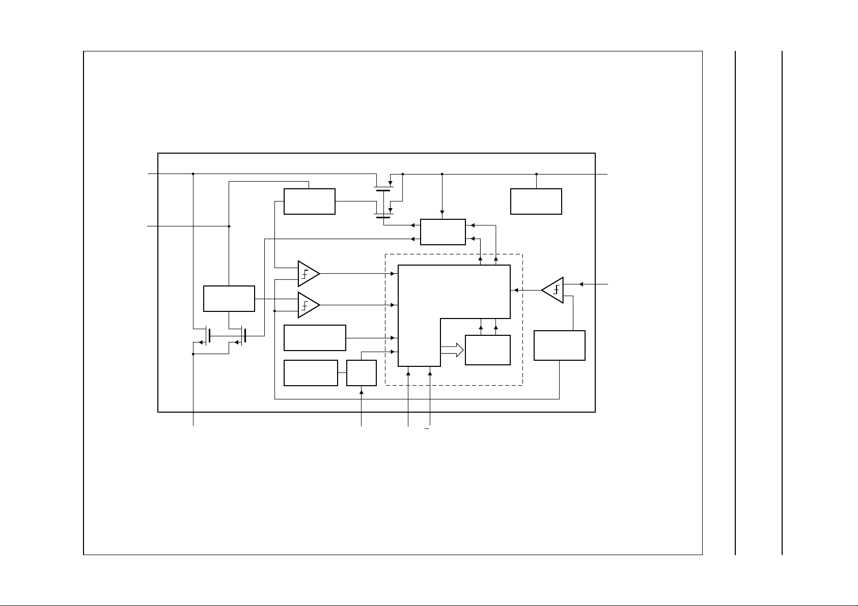
BLOCK DIAGRAM
Philips Semiconductors Product specification
High efficiency DC/DC converter TEA1207T
LX
ILIM
4
I/V
CONVERTER
2
CURRENT LIMIT
COMPARATORS
TEMPERATURE
PROTECTION
13 MHz
OSCILLATOR
N-type
POWER
FET
I/V
CONVERTER
sense
FET
GND
P-type POWER FET
SYNC
GATE
5681
SYNC U/D
sense FET
SHDWN
START-UP
CIRCUIT
CONTROL LOGIC
AND
MODE GEARBOX
TIME
COUNTER
DIGITAL CONTROLLER
INTERNAL
SUPPLY
TEA1207T
BAND GAP
REFERENCE
3
7
MGR665
UPOUT/DNIN
FB
Fig.1 Block diagram.
Philips Semiconductors Product specification
High efficiency DC/DC converter TEA1207T
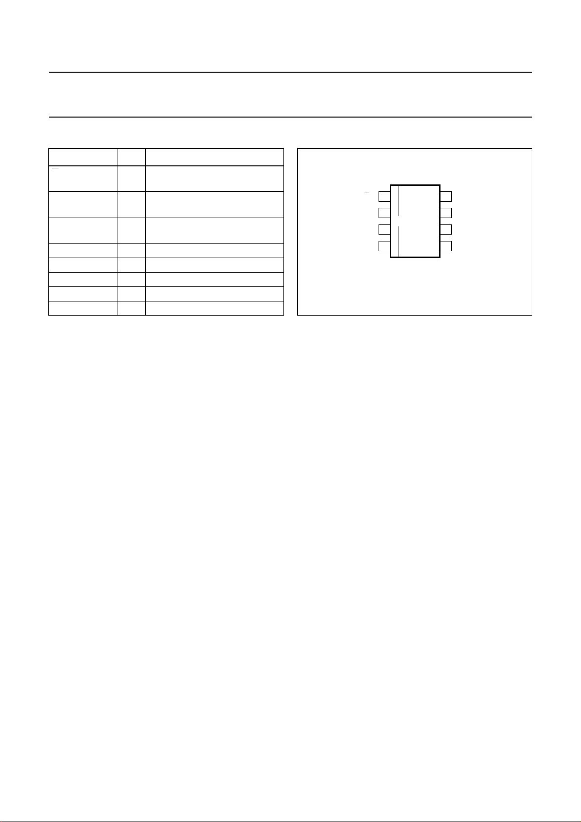
PINNING
SYMBOL PIN DESCRIPTION
U/D 1 up-or-down mode selection
input; active LOW for up mode
ILIM 2 current limiting resistor
connection
UPOUT/DNIN 3 output voltage in up mode;
input voltage in down mode
LX 4 inductor connection
SYNC 5 synchronization clock input
GND 6 ground
FB 7 feedback input
SHDWN 8 shut-down input
handbook, halfpage
UPOUT/DNIN GND
1
U/D SHDWN
2
ILIM FB
TEA1207T
3
4
LX SYNC
8
7
6
5
MGR666
Fig.2 Pin configuration.
FUNCTIONAL DESCRIPTION
Control mechanism
TheTEA1207TDC/DCconverterisabletooperatein PFM
(discontinuous conduction) or PWM (continuous
conduction) operating mode. All switching actions are
completely determined by a digital control circuit which
usesthe output voltage level as its controlinput.Thisnovel
digital approach enables the use of a new pulse width and
frequency modulation scheme, which ensures optimum
power efficiency over the complete operating range of the
converter.
When high output power is requested, the device will
operate in PWM (continuous conduction) operating mode.
This results in minimum AC currents in the circuit
components and hence optimum efficiency, minimum
costs and low EMC. In this operating mode, the output
voltage is allowed to vary between two predefined voltage
levels. As long as the output voltage stays within this
so-called window, switching continues in a fixed pattern.
When the output voltage reaches one of the window
borders, the digital controller immediately reacts by
adjusting the pulse width and inserting a current step in
such a way that the output voltage stays within the window
with higher or lower current capability. This approach
enables very fast reaction to load variations. Figure 3
shows the converter’s response to a sudden load
increase. The upper trace shows the output voltage.
The ripple on top of the DC level is a result of the current
in the output capacitor, which changes in sign twice per
cycle, times the capacitor’s internal Equivalent Series
Resistance (ESR). After each ramp-down of the inductor
current, i.e. when the ESR effect increases the output
voltage, the converter determines what to do in the next
cycle. As soon as more load current is taken from the
output the output voltage starts to decay.
When the output voltage becomes lower than the low limit
of the window, a corrective action is taken by a ramp-up of
theinductorcurrentduringa much longer time. As a result,
the DC current level is increased and normal PWM control
can continue. The output voltage (including ESR effect) is
again within the predefined window. Figure 4 depicts the
spread of the output voltage window. The absolute value
ismostdependent on spread, while the actual window size
is not affected. For one specific device, the output voltage
will not vary more than 2% typically.
In low output power situations, the TEA1207T will switch
over to PFM (discontinuous conduction) operating mode.
In this mode, regulation information from earlier PWM
operating modes is used. This results in optimum inductor
peak current levels in the PFM mode, which are slightly
larger than the inductor ripple current in the PWM mode.
As a result, the transition between PFM and PWM mode is
optimum under all circumstances. In the PFM mode the
TEA1207Tregulates the output voltage to the high window
limit as shown in Fig.3.
Synchronous rectification
For optimum efficiency over the whole load range,
synchronous rectifiers inside the TEA1207T ensure that
during the whole second switching phase, all inductor
current will flow through the low-ohmic power MOSFETs.
Special circuitry is included which detects that the inductor
current reaches zero. Following this detection, the digital
controller switches off the power MOSFET and proceeds
regulation.
2000 Nov 27 5

Philips Semiconductors Product specification
High efficiency DC/DC converter TEA1207T
Start-up
Start-up from low input voltage in boost mode is realized
by an independent start-up oscillator, which starts
switching the N-type power MOSFET as soon as the
voltage at pin UPOUT/DNIN is measured to be sufficiently
high. The switch actions of the start-up oscillator will
increase the output voltage. As soon as the output voltage
is high enough for normal regulation, the digital control
system takes over the control of the power MOSFETs.
Undervoltage lockout
As a result of too high load or disconnection of the input
power source, the output voltage can drop so low that
normal regulation cannot be guaranteed. In that case, the
device switches back to start-up mode. If the output
voltage drops down even further, switching is stopped
completely.
Shut-down
When the shut-down input is made HIGH, the converter
disables both power switches and the power consumption
is reduced to a few microamperes.
Power switches
The power switches in the IC are one N-type and one
P-type power MOSFET, having a typical drain-to-source
resistance of 0.20 Ω and 0.22 Ω respectively.
The maximum average current in the power switches is
0.60 A at T
Temperature protection
When the device operates in PWM mode, and the die
temperature gets too high (typically 175 °C), the converter
stops operating. It resumes operation when the die
temperature falls below 175 °C again. As a result,
low-frequent cycling between the on and off state will
occur. It should be noted that in the event of a device
temperature around the cut-off limit, the application differs
strongly from maximum specifications.
amb
=80°C.
Current limiters
If the current in one of the power switches exceeds its limit
in the PWM mode, the current ramp is stopped
immediately, and the next switching phase is entered.
Currentlimiting is required to enable optimal use of energy
in Li-ion batteries, and to keep power conversion efficient
during temporary high loads. Furthermore, current limiting
protects the IC against overload conditions, inductor
saturation, etc. The current limiting level is set by an
external resistor.
External synchronization
If an external high-frequency clock is applied to the
synchronization clock input, the switching frequency in
PWM mode will be exactly that frequency divided by 22.
In thePFMmode, the switching frequency is always lower.
The quiescent current of the device increases when
external clock pulses are applied. In case no external
synchronization is necessary, the synchronization clock
input must be connected to ground level.
Behaviour at input voltage exceeding the specified
range
In general, an input voltage exceeding the specified range
isnot recommended since instability may occur. There are
two exceptions:
• Upconversion: at an input voltage higher than the target
output voltage, but up to 6 V, the converter will stop
switchingand the internal P-type power MOSFET will be
conducting. The output voltage will equal the input
voltage minus some resistive voltage drop. The current
limiting function is not active.
• Downconversion: when the input voltage is lower than
the target output voltage, but higher than 2.8 V, the
P-type power MOSFET will stay conducting resulting in
an output voltage being equal to the input voltage minus
some resistive voltage drop. The current limiting
function remains active.
2000 Nov 27 6
 Loading...