

Philips TEA1118AT, TEA1118AM, TEA1118T, TEA1118M Datasheet

INTEGRATED CIRCUITS
DATA SH EET
TEA1118; TEA1118A
Versatile cordless transmisssion
circuit
Product specification
Supersedes data of 1996 Nov 26
File under Integrated Circuits, IC03
1997 Jul 14
Philips Semiconductors Product specification
Versatile cordless transmisssion circuit TEA1118; TEA1118A
FEATURES
• Low DC line voltage; operates down to 1.6 V (excluding
polarity guard)
• Voltage regulator with adjustable DC voltage
• Provides a supply for external circuits
• Symmetrical high impedance transmit inputs (62.5 kΩ)
with large signals handling capabilities [up to
1 V (RMS value) with less than 2% THD]
• Receive amplifier for dynamic, magnetic or
piezoelectric earpieces
• AGC line loss compensation for transmit and earpiece
amplifiers
• DTMF input with confidence tone (TEA1118A only)
• MUTE input for pulse or DTMF dialling (TEA1118A only)
• Transmit mute function, also enabling the DTMF input
(TEA1118A only).
APPLICATIONS
• Cordless telephone base stations
• Fax machines
• Answering machines.
GENERAL DESCRIPTION
The TEA1118 and TEA1118A are bipolar integrated
circuits that perform all speech and line interface functions
required in cordless telephone base stations. The ICs
operate at a line voltage down to 1.6 V DC (with reduced
performance) to facilitate the use of telephone sets
connected in parallel.
The TEA1118A offers in addition to the TEA1118
electronic switching between speech and dialling.
Moreover the transmit amplifier can be disabled during
speech condition by means of a transmit mute function.
All statements and values refer to all versions unless
otherwise specified.
QUICK REFERENCE DATA
I
= 15 mA; VEE=0V; R
line
=20Ω; AGC pin connected to VEE; Z
SLPE
= 600 Ω; f = 1 kHz; T
line
amb
=25°C;
unless otherwise specified.
SYMBOL PARAMETER CONDITIONS MIN. TYP. MAX. UNIT
I
line
line current operating range normal operation 11 − 140 mA
with reduced performance 1 − 11 mA
V
I
CC
V
G
∆G
LN
CC
vtrx
vtrx
DC line voltage 3.35 3.65 3.95 V
internal current consumption VCC= 2.9 V − 1.15 1.4 mA
supply voltage for peripherals IP=0mA − 2.9 − V
typical voltage gain range
transmit amplifier (TEA1118A only) V
transmit amplifier (TEA1118 only) V
receive amplifier V
gain control range for transmit and
= 200 mV (RMS) −−11.3 dB
TX
= 200 mV (RMS) 5.3 − 11.3 dB
TX
= 4 mV (RMS) 19 − 31 dB
IR
I
=75mA − 5.8 − dB
line
receive amplifiers with respect to
I
=15mA
line
1997 Jul 14 2
Philips Semiconductors Product specification
Versatile cordless transmisssion circuit TEA1118; TEA1118A
ORDERING INFORMATION
TYPE
NUMBER
NAME DESCRIPTION VERSION
TEA1118M SSOP16
TEA1118T SO14
TEA1118AM SSOP16
TEA1118AT SO14
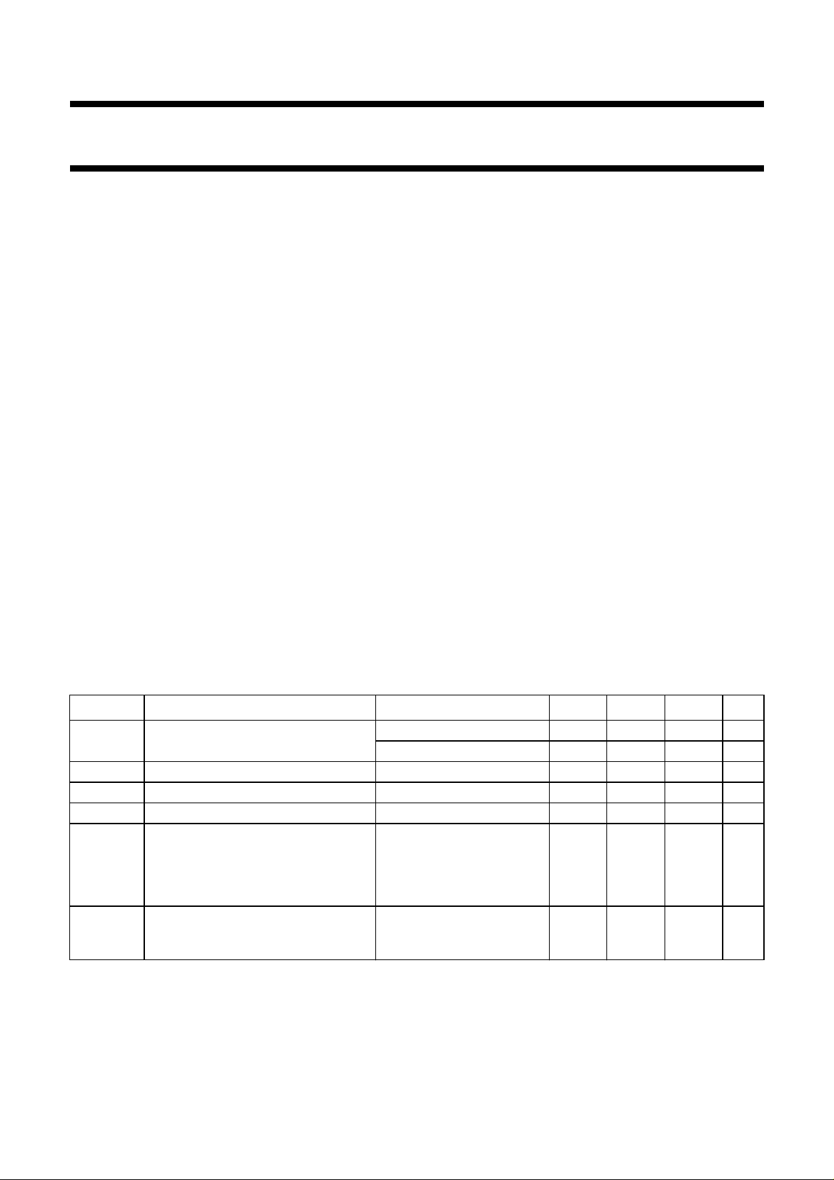
BLOCK DIAGRAMS
handbook, full pagewidth
IR
PACKAGE
plastic shrink small outline package; 16 leads; body width 4.4 mm
plastic small outline package; 14 leads; body width 3.9 mm
plastic shrink small outline package; 16 leads; body width 4.4 mm
plastic small outline package; 14 leads; body width 3.9 mm
GAR
V−>I
QR
CURRENT
REFERENCE
V
LN
CC
SOT369-1
SOT108-1
SOT369-1
SOT108-1
TX+
TX−
V−>I
V
EE
AGC
CIRCUIT
AGC
TEA1118M
TEA1118T
LOW VOLTAGE
CIRCUIT
Fig.1 Block diagram (TEA1118).
GAT
REG
MBH273
SLPE
1997 Jul 14 3
Philips Semiconductors Product specification
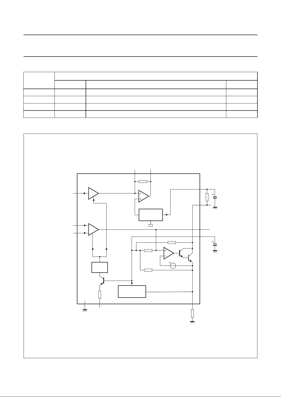
Versatile cordless transmisssion circuit TEA1118; TEA1118A
handbook, full pagewidth
DTMF
TMUTE
TX+
TX−
GAR
IR
ATTENUATOR
TRANSMIT
MUTE
V−>I
V−>I
V−>I
V−>I
CIRCUIT
AGC
CURRENT
REFERENCE
QR
MUTE
V
CC
LN
REG
TEA1118AM
TEA1118AT
LOW VOLTAGE
CIRCUIT
V
EE
AGC
Fig.2 Block diagram (TEA1118A).
1997 Jul 14 4
MBH272
SLPE
Philips Semiconductors Product specification
Versatile cordless transmisssion circuit TEA1118; TEA1118A
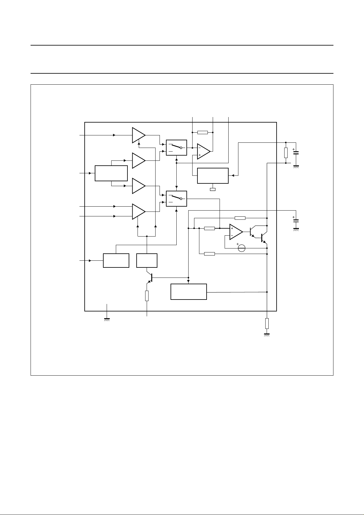
PINNING
SYMBOL
LN 1111positive line terminal
SLPE 2222slope (DC resistance) adjustment
REG 3333line voltage regulator decoupling
GAT 4 4 −−transmit gain adjustment
TMUTE −−4 5 transmit mute input
DTMF −−5 6 dual-tone multi-frequency input
MUTE −−6 8 mute input to select speech or dialling mode
IR 7979receive amplifier input
AGC 8 10 8 10 automatic gain control/line loss compensation
TX− 9 11 9 11 inverting transmit amplifier input
TX+ 10 12 10 12 non-inverting transmit amplifier input
V
EE
QR 12 14 12 14 receive amplifier output
GAR 13 15 13 15 receive gain adjustment
V
CC
n.c. 5 and 6 5 to 8 − 4 and 7 not connected
TEA1118 TEA1118A
DESCRIPTION
SO14 SSOP16 SO14 SSOP16
11 13 11 13 negative line terminal
14 16 14 16 supply voltage for speech circuit and peripherals
1997 Jul 14 5
Philips Semiconductors Product specification
Versatile cordless transmisssion circuit TEA1118; TEA1118A
handbook, halfpage
Fig.3 Pin configuration (TEA1118T).
1
LN
2
SLPE GAR
3
REG QR
4
GAT
n.c. TX+
n.c. TX−
TEA1118T
5
6
7
IR AGC
MBH269
V
14
CC
13
12
V
11
EE
10
9
8
handbook, halfpage
Fig.4 Pin configuration (TEA1118M).
1
LN
2
SLPE GAR
3
REG QR
GAT
4
TEA1118M
5
n.c. TX+
6
n.c. TX−
7
n.c. AGC
8
n.c. IR
MBH268
V
16
CC
15
14
V
13
EE
12
11
10
9
handbook, halfpage
1
LN
2
SLPE GAR
3
REG QR
TMUTE
4
TEA1118AT
5
DTMF TX+
6
MUTE TX−
7
IR AGC
MBH271
V
14
CC
13
12
V
11
EE
10
9
8
Fig.5 Pin configuration (TEA1118AT).
1997 Jul 14 6
handbook, halfpage
Fig.6 Pin configuration (TEA1118AM).
1
LN
2
SLPE GAR
3
REG QR
n.c.
4
TEA1118AM
TMUTE TX+
5
6
DTMF TX−
7
n.c. AGC
8
MUTE IR
MBH270
V
16
CC
15
14
V
13
EE
12
11
10
9

Philips Semiconductors Product specification
Versatile cordless transmisssion circuit TEA1118; TEA1118A
FUNCTIONAL DESCRIPTION
All data given in this chapter are typical values, except
when otherwise specified.
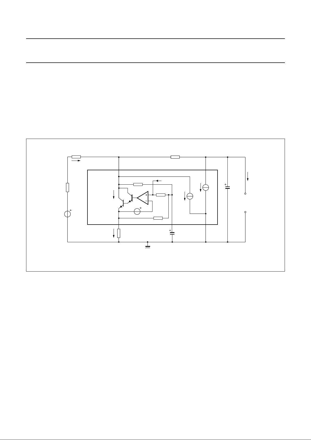
Supplies (pins LN, SLPE, V
and REG)
CC
The supply for the TEA1118 and TEA1118A and their
peripherals is obtained from the telephone line.
The ICs generate a stabilized reference voltage (V
ref
)
between pins LN and SLPE. This reference voltage is
equal to 3.35 V, is temperature compensated and can be
adjusted by means of an external resistor (RVA). It can be
increased by connecting the RVA resistor between
pins REG and SLPE (see Fig.11), or decreased by
connecting the RVA resistor between pins REG and LN.
The voltage at pin REG is used by the internal regulator to
generate the stabilized reference voltage and is decoupled
by a capacitor (C
) which is connected to VEE.
REG
This capacitor, converted into an equivalent inductance
(see Section “Set impedance”), realizes the set impedance
conversion from its DC value (R
) to its AC value
SLPE
(RCC in the audio-frequency range). The voltage at pin
SLPE is proportional to the line current. Figure 7 illustrates
the supply configuration.
The ICs regulate the line voltage at pin LN, and it can be
calculated as follows:
VLN=V
I
SLPE=Iline
ref+RSLPE
− ICC− IP− I* = I
× I
SLPE
sh
where:
I
: line current
line
ICC: current consumption of the IC
IP: supply current for peripheral circuits
I*: current consumed between LN and V
EE
Ish: the excess line current shunted to SLPE (and VEE)
via LN.
The preferred value for R
is 20 Ω. Changing R
SLPE
SLPE
will
affect more than the DC characteristics; it also influences
the transmit gain and the DTMF gain (TEA1118A only), the
gain control characteristics, the sidetone level and the
maximum output swing on the line.
by the formula (see also Figs 8 and 9). R
CCint
is the
internal equivalent resistance of the voltage supply point,
and I
is the current consumed by the output stage of the
rec
earpiece amplifier.
VCC=V
V
CC0=VLN
CC0
− RCC× I
− R
CCint
× (IP− I
CC
rec
)
The DC line current flowing into the set is determined by
the exchange supply voltage (V
resistance (R
(R
) and the reference voltage (V
line
), the DC resistance of the telephone line
exch
), the feeding bridge
exch
). With line currents
ref
below 7.5 mA, the internal reference voltage (generating
V
) is automatically adjusted to a lower value.
ref
This means that more sets can operate in parallel with DC
line voltages (excluding the polarity guard) down to an
absolute minimum voltage of 1.6 V. At currents below
7.5 mA, the circuit has limited transmit and receive levels.
This is called the low voltage area.
Set impedance
In the audio frequency range, the dynamic impedance is
mainly determined by the R
resistor. The equivalent
CC
impedance of the circuits is illustrated in Fig.10.
Transmit amplifier (pins TX+, TX− and GAT)
The TEA1118 and TEA1118A have symmetrical transmit
inputs. The input impedance between pins TX+ and TX− is
equal to 62.5 kΩ; the input impedance between pins
TX+/TX− and V
is equal 36.5 kΩ. The voltage gain from
EE
pins TX+/TX− to pin LN is set at 11.3 dB.
Automatic gain control is provided on this amplifier for line
loss compensation.
The gain of the TEA1118 can be decreased by connecting
an external resistor R
The adjustment range is equal to 6 dB. A capacitor C
between pins GAT and REG.
GAT
GAT
connected between pins GAT and REG can be used to
provide a first-order low-pass filter. The cut-off frequency
corresponds to the time constant C
R
is the internal resistor which sets the gain with a
GATint
GAT
×(R
GATint
// R
GAT
typical value of 27 kΩ.
Transmit mute (pin TMUTE; TEA1118A only)
).
The internal circuitry of the TEA1118 and TEA1118A is
supplied from pin VCC. This voltage supply is derived from
the line voltage by means of a resistor (RCC) and must be
decoupled by a capacitor C
. It may also be used to
VCC
supply peripheral circuits such as dialling or control
circuits. The VCC voltage depends on the current
consumed by the IC and the peripheral circuits as shown
1997 Jul 14 7
The transmit amplifier can be disabled by activating the
transmit mute function. When TMUTE is LOW, the normal
speech mode is entered, depending on the level on MUTE.
When TMUTE is HIGH, the transmit amplifier inputs are
disabled while the DTMF input is enabled (no confidence
tone is provided). The voltage gain between LN and
TX+/TX− is attenuated; the gain reduction is 80 dB.
Philips Semiconductors Product specification
h
Versatile cordless transmisssion circuit TEA1118; TEA1118A
Receive amplifier (pins IR, GAR and QR)
The receive amplifier has one input (IR) and one output
(QR). The input impedance between pins IR and VEE is
20 kΩ. The voltage gain from pin IR to pin QR is set at
31 dB. The gain can be decreased by connecting an
external resistor R
between pins GAR and QR; the
GAR
adjustment range is 12 dB. Two external capacitors C
(connected between GAR and QR) and C
GARS
(connected
between GAR and VEE) ensure stability.
R
R
line
I
line
exch
V
exch
TEA1118
TEA1118A
I
sh
I
SLPE
LN
SLPE
R
SLPE
20 Ω
andbook, full pagewidth
GAR
The C
capacitor provides a first-order low-pass filter.
GAR
The cut-off frequency corresponds to the time constant
C
GAR
× (R
GARint
// R
GAR
). R
is the internal resistor
GARint
which sets the gain with a typical value of 100 kΩ. The
condition C
GARS
=10×C
must be fulfilled to ensure
GAR
stability.
Automatic gain control is provided on this amplifier for line
loss compensation.
R
CC
619 Ω
V
from preamp
REG
C
REG
4.7 µF
CC
I
CC
*
I
V
EE
C
VCC
100 µF
MBH274
peripheral
circuits
I
p
Fig.7 Supply configuration.
1997 Jul 14 8
 Loading...