

Philips tea1114a DATASHEETS

INTEGRATED CIRCUITS
DATA SH EET
TEA1114A
Low voltage telephone
transmission circuit with dialler
interface and regulated strong
supply
Product specification
Supersedes data of 1999 Sep 14
File under Integrated Circuits, IC03
2000 Mar 21
Philips Semiconductors Product specification
Low voltage telephone transmission circuit with
dialler interface and regulated strong supply
FEATURES
• Low DC line voltage; operates down to 1.45 V
(excluding voltage drop over external polarity guard)
• Line voltage regulator with adjustable DC voltage
• 3.3 V regulated strong supply point for peripheral
circuits compatible with:
– Speech mode
– Ringer mode
– Trickle mode.
• Transmit stage with:
– Microphone amplifier with symmetrical high
impedance inputs
– DTMF amplifier with confidence tone on receive
output.
• Receive stage with:
– Receive amplifier with asymmetrical output
– Earpiece amplifier with adjustable gain (and gain
boost facility) for all types of earpieces.
• MUTE input for pulse or DTMF dialling
• AGClinelosscompensationformicrophoneandreceive
amplifiers.
APPLICATIONS
• Line powered telephone sets with LCD module
• Cordless telephones
• Fax machines
• Answering machines.
GENERAL DESCRIPTION
The TEA1114A is a bipolar integrated circuit that performs
all speech and line interface functions required in fully
electronic telephone sets. It performs electronic switching
between speech and dialling. The IC operates at a line
voltage down to 1.45 V DC (with reduced performance) to
facilitate the use of telephone sets connected in parallel.
When the line current is high enough, a fixed amount of
current is derived from the LN pin in order to create a
strong supply point at pin VDD. The voltage at pin VDD is
regulated to 3.3 V to supply peripherals such as dialler,
LCD module and microcontroller.
TEA1114A
ORDERING INFORMATION
TYPE
NUMBER
TEA1114A DIP16 plastic dual in-line package; 16 leads (300 mil) SOT38-4
TEA1114AT SO16 plastic small outline package; 16 leads; body width 3.9 mm SOT109-1
TEA1114AUH − bare die; on foil −
NAME DESCRIPTION VERSION
PACKAGE
2000 Mar 21 2
Philips Semiconductors Product specification
Low voltage telephone transmission circuit with
TEA1114A
dialler interface and regulated strong supply
QUICK REFERENCE DATA
I
= 15 mA; VEE=0V;R
line
circuits given in Figs 15, 16 and 17; T
specified.
SYMBOL PARAMETER CONDITIONS MIN. TYP. MAX. UNIT
I
V
I
V
line
LN
CC
CC
line current operating range normal operation 11 − 140 mA
DC line voltage 4.05 4.35 4.65 V
internal current consumption VCC= 3.6 V − 1.25 1.5 mA
supply voltage for internal circuitry
(unregulated)
V
DD
regulated supply voltage for peripherals
speech mode I
ringer mode I
I
DD
G
v(TX)
available supply current for peripherals −−−3mA
typical voltage gain for microphone
amplifier
G
∆G
∆G
v(RX)
v(QR)
v(trx)
typical voltage gain for receiving amplifier VIR= 4 mV (RMS) 32.4 33.4 34.4 dB
gain setting range for earpiece amplifier RE1= 100 kΩ−14 − +12 dB
gain control range for microphone and
receive amplifiers with respect to
I
=15mA
line
∆G
v(trx)(m)
gain reduction for microphone and receive
amplifiers
=20Ω;AGC pin connected to VEE;Z
SLPE
=25°C for TEA1114A(T); Tj=25°C for TEA1114AUH; unless otherwise
amb
= 600 Ω; f = 1 kHz; measured according to test
line
with reduced performance 1 − 11 mA
IP=0mA − 3.6 − V
= −3 mA 3.0 3.3 3.6 V
DD
= 75 mA 3.0 3.3 3.6 V
DD
V
= 4 mV (RMS) 43.2 44.2 45.2 dB
MIC
I
=85mA − 6.0 − dB
line
MUTE = LOW − 80 − dB
2000 Mar 21 3
Philips Semiconductors Product specification
Low voltage telephone transmission circuit with
dialler interface and regulated strong supply
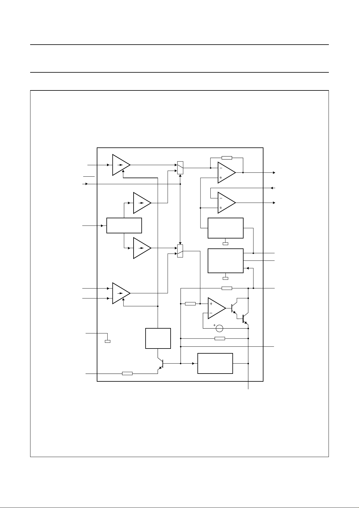
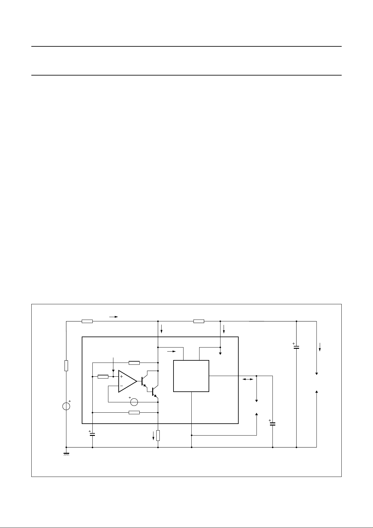
BLOCK DIAGRAM
handbook, full pagewidth
48IR
VI
MUTE
VI
6DTMF
ATTENUATOR
0.5V
CC
TEA1114A
1211RX
GAR
9QR
CURRENT AND
VOLTAGE
REFERENCE
MIC+
MIC−
V
EE
AGC
VI
V
DD
REGULATOR
V
16
CC
V
7
DD
TEA1114A
13
VI
14
10
AGC
CIRCUIT
LOW VOLTAGE
5
CIRCUIT
SLPE
1LN
3 REG
2
MGK804
Fig.1 Block diagram.
2000 Mar 21 4
Philips Semiconductors Product specification
Low voltage telephone transmission circuit with
TEA1114A
dialler interface and regulated strong supply
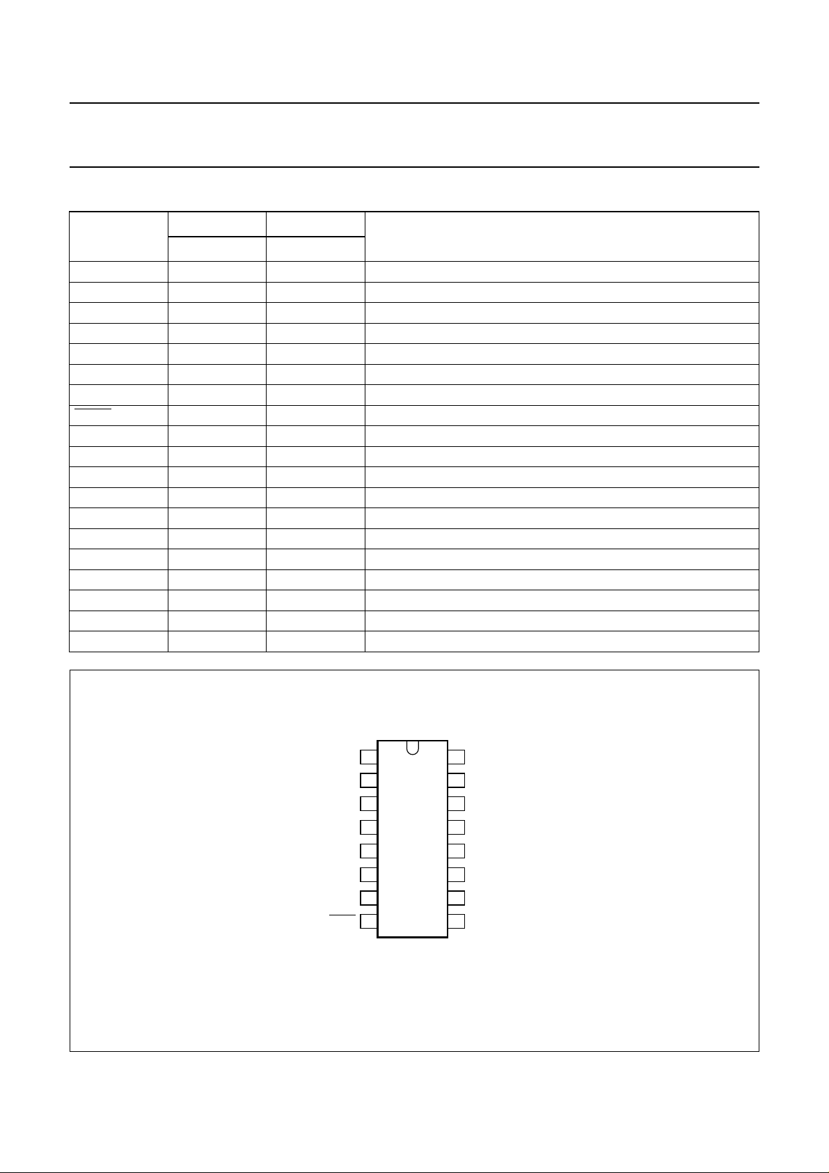
PINNING
SYMBOL
LN 1 1, 19 positive line terminal
SLPE 2 2 slope (DC resistance) adjustment
REG 3 3 line voltage regulator decoupling
IR 4 4 receiving amplifier input
AGC 5 5 automatic gain control/ line loss compensation
DTMF 6 6 dual-tone multi-frequency input
V
DD
MUTE 8 8 mute input to select speech or dialling mode (active LOW)
QR 9 9 earpiece amplifier output
n.c. − 10 not connected
V
EE
n.c. − 12 not connected
GAR 11 13 earpiece amplifier gain adjustment
RX 12 14 receive amplifier output
MIC+ 13 15 non-inverting microphone amplifier input
MIC− 14 16 inverting microphone amplifier input
n.c. 15 − not connected
V
CC
n.c. − 18 not connected
PIN PAD
DESCRIPTION
TEA1114A(T) TEA1114AUH
7 7 regulated supply for peripherals
10 11 negative line terminal
16 17 supply voltage for internal circuit
handbook, halfpage
LN
SLPE
REG
AGC
DTMF
V
DD
MUTE
IR
1
2
3
4
TEA1114A
5
6
7
8
Fig.2 Pin configuration.
2000 Mar 21 5
MGK803
V
16
CC
n.c.
15
14
MIC−
13
MIC+
12
RX
11
GAR
V
10
EE
QR
9
Philips Semiconductors Product specification
Low voltage telephone transmission circuit with
dialler interface and regulated strong supply
FUNCTIONAL DESCRIPTION
All data given in this chapter are typical values, except
when otherwise specified.
Supply (pins LN, SLPE, REG, VCCand VDD)
The supply for the TEA1114A and its peripherals is
obtained from the telephone line (see Fig.3).
HE LINE INTERFACE (PINS LN, SLPE AND REG)
T
The IC generates a stabilized reference voltage (V
between pins LN and SLPE. V
is temperature
ref
ref
)
compensated and can be adjusted by means of an
external resistor (RVA). V
equals 4.15 V and can be
ref
increased by connecting RVA between pins REG and
SLPE or decreased by connecting R
between pins
VA
REG and LN. The voltage at pin REG is used by the
internal regulator to generate V
C
, which is connected to VEE. This capacitor,
REG
and is decoupled by
ref
converted into an equivalent inductance
(see Section “Set impedance”)realizesthesetimpedance
conversion from its DC value (R
) to its AC value
SLPE
(RCCin the audio-frequency range). The voltage at
pin SLPE is proportional to the line current.
The voltage at pin LN is:
I
SLPE
where:
I
line
ICC= current consumption of the IC
IP= supply current for external circuits
I
SUP
VDD regulator.
Thepreferredvalue for R
affect more than the DC characteristics; it also influences
the microphone and DTMF gains, the gain control
characteristics, the sidetone level and the maximum
output swing on the line.
The DC line current flowing into the set is determined by
the exchange supply voltage (V
resistance (R
line (R
currents below 9 mA, the internal reference voltage
(generatingV
This means that more sets can operate in parallel with
DC line voltages (excluding the polarity guard) down to an
absolute minimum voltage of 1.45 V. At currents below
9 mA, the circuit has limited sending and receiving levels.
This is called the low voltage area.
TEA1114A
I=
ICC– IP– I
line
= line current
= current consumed between LN and VEE by the
EXCH
) and the reference voltage (V
line
ref
–
SUP
is 20 Ω.ChangingR
SLPE
), the feeding bridge
EXCH
SLPE
), the DC resistance of the telephone
). With line
ref
)isautomatically adjusted to a lower value.
will
V
=
V
LN
handbook, full pagewidth
refRSLPE
R
EXCH
V
EXCH
I×+
SLPE
R
line
TEA1114A
from preamplifier
REG SLPE
C
REG
4.7 µF
I
line
I
SLPE
R
CC
I
LN
LN
R
SLPE
20 Ω
I
SUP
V
DD
REGULATOR
V
CC
internal
circuitry
V
EE
Fig.3 Supply configuration.
I
V
CC
DD
I
DD
peripherals
C
VCC
100 µF
C
VDD
220 µF
external
circuits
MGK805
I
P
2000 Mar 21 6
Philips Semiconductors Product specification
Low voltage telephone transmission circuit with
dialler interface and regulated strong supply
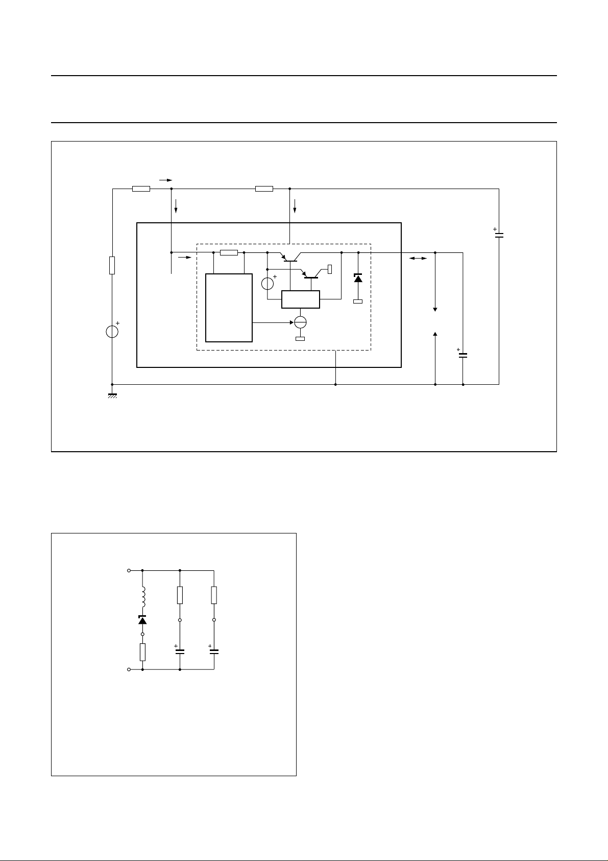
THE INTERNAL SUPPLY POINT (PIN VCC)
The internal circuitry of the TEA1114A is supplied from
pin V
voltage by means of a resistor (R
decoupled by a capacitor C
supply some external circuits. The V
on the current consumed by the IC and the peripheral
circuits as:
V
(seealso Figs 4 and 5). I
output stage of the earpiece amplifier.
. This voltage supply is derived from the line
CC
) and must be
CC
. It may also be used to
VCC
V
CC
handbook, halfpage
CC0RCCIPIrec
CC0
R
CC
VLNR
V
V
×–=
CCICC
+()×–=
isthe current consumed by the
rec
CC
voltage depends
CC
handbook, halfpage
(mA)
TEA1114A
3
I
P
1.9 mA
2
1.6 mA
1
0
0
12 43
(2) (1)
MGL827
VCC (V)
V
CC0
I
rec
V
EE
EXTERNAL
CIRCUITS
I
MGK806
P
Fig.4 VCC used as supply voltage for external
circuits.
THE REGULATED SUPPLY POINT (PIN VDD)
The V
regulator delivers a stabilized voltage for the
DD
peripherals in transmission mode (nominal VLN) as well as
in ringer mode (VLN= 0 V). The regulator (see Fig.6)
consistsofa sense input circuit, a current switchandaV
DD
output stabilizer. The regulator operates as a current
source at the LN input in transmission mode; it takes a
constant current of 4.3 mA (at nominal conditions) from
pin LN. The current switch reduces the distortion on the
line at large signal swings. Output VDD follows the
DC voltage at pin LN (with typically 0.35 V difference) up
to VDD= 3.3 V. The input current of the regulator is
constantwhiletheoutput(source)currentis determined by
the consumption of the peripherals. The difference
betweeninputand output current is shunted bytheinternal
stabilizer.
V
DD
VCC≥ 2.5 V; VLN= 4.35 V at I
=20Ω.
R
SLPE
Curve (1) is valid when the receiving amplifier is driven:
= 150 mV; RL1= 150 Ω.
V
QR(rms)
Curve (2) is valid when the receiving amplifier is not driven.
= 15 mA; RCC= 619 Ω;
line
Fig.5 Typical current IP available from VCC for
peripheral circuitry.
Inringer mode, the stabilizer operates as ashunt stabilizer
to keep V
at 3.3 V. In this mode, the input voltage
DD
VLN= 0 V while the input current into pin VDD is delivered
by the ringing signal. VDD has to be decoupled by a
capacitor C
VDD
.
2000 Mar 21 7
Philips Semiconductors Product specification
Low voltage telephone transmission circuit with
dialler interface and regulated strong supply
handbook, full pagewidth
R
EXCH
V
EXCH
R
line
TEA1114A
I
LN
line
I
I
LN
SUP
SENSE
R
CC
I
CC
V
CC
SWITCH
VDD regulator
TEA1114A
C
VCC
V
DD
I
DD
peripherals
C
V
EE
220 µF
100 µF
VDD
MGK807
Fig.6 VDD regulator configuration.
Set impedance
In the audio frequency range, the dynamic impedance is
mainly determined by the RCC resistor. The equivalent
impedance of the circuit is illustrated in Fig.7.
REG
× R
V
LN
SLPE
EE
SLPE
× RP.
L
EQ
V
R
20 Ω
ref
SLPE
R
P
REG V
C
REG
4.7 µF
R
CC
619 Ω
CC
C
VCC
100 µF
MBE788
handbook, halfpage
LEQ=C
RP= internal resistance.
RP= 17.5 kΩ.
Transmit stage (pins MIC+, MIC− and DTMF)
MICROPHONE AMPLIFIER (PINS MIC+ AND MIC−)
The TEA1114A has symmetrical microphone inputs.
The input impedance between pins MIC+ and MIC− is
64 kΩ (2 × 32 kΩ). Thevoltage gain from pins MIC+/MIC−
to pin LN is set at 44.2 dB (typically).
Automatic gain control is provided on this amplifier for line
loss compensation.
DTMF AMPLIFIER (PIN DTMF)
When the DTMF amplifier is enabled, dialling tones may
be sent on line. These tones are also sent to the receive
output RX at a low level (confidence tone).
The TEA1114A has an asymmetrical DTMF input.
The input impedance between DTMF and VEE is 20 kΩ.
The voltage gain from pin DTMF to pin LN is set at 26 dB.
Automatic gain control has no effect on the DTMF
amplifier.
Fig.7 Equivalent impedance between LN and VEE.
2000 Mar 21 8
Philips Semiconductors Product specification
Low voltage telephone transmission circuit with
dialler interface and regulated strong supply
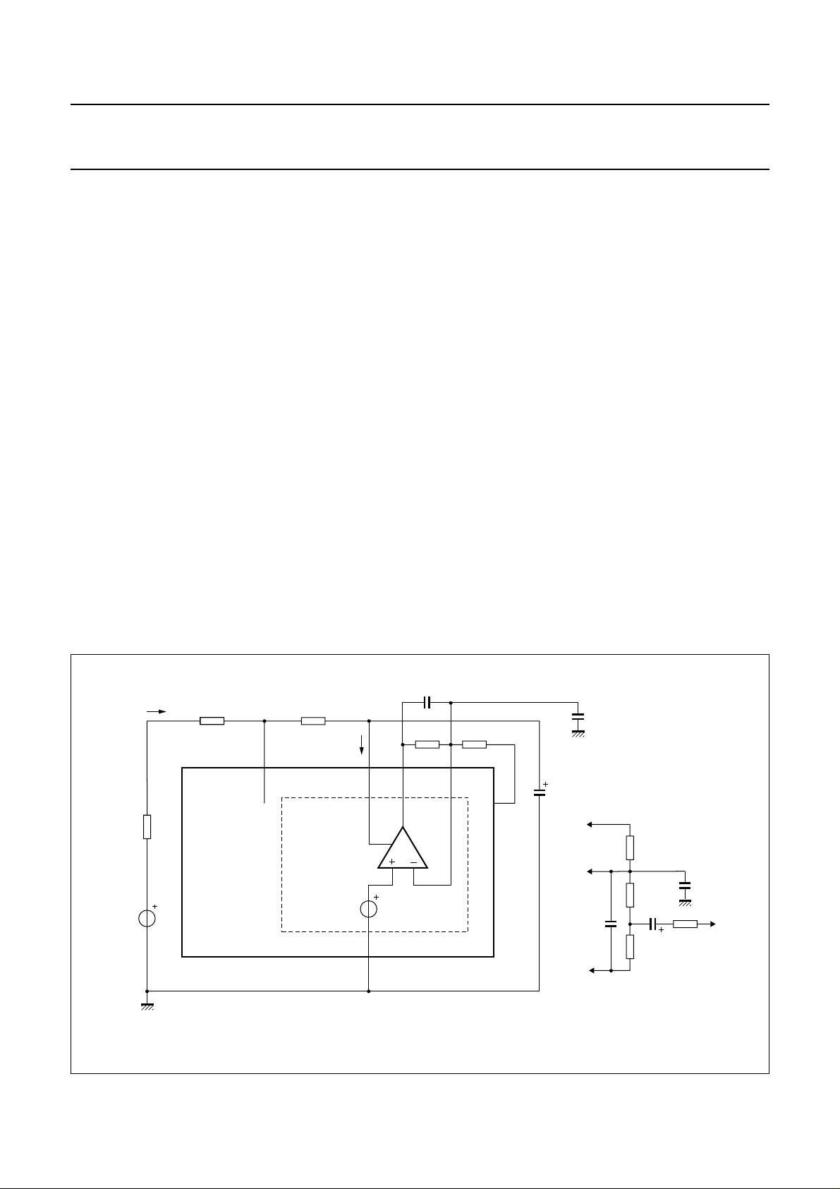
Receiving stage (pins IR, RX, GAR and QR)
The receive part consists of a receive amplifier and an
earpiece amplifier.
THE RECEIVE AMPLIFIER (PINS IR AND RX)
The receive amplifier transfers the receive signal from
input IR to output RX. The input impedance of the receive
amplifier, between pins IR and VEE,is20kΩ. The voltage
gain from pin IR to RX is set at 33.4 dB. RX output is
intended to drive high ohmic (real) loads. Automatic gain
control is provided on the receive amplifier.
THE EARPIECE AMPLIFIER (PINS GAR AND QR)
The earpiece amplifier is an operational amplifier having
its output (QR) and inverting input (GAR) available. It can
be used in conjunction with two resistors to get someextra
gain or attenuation.
In an usual configuration (see Fig.8), output RX drives the
earpiece amplifier by means of RE1 connected between
RX and GAR. Feedback resistor RE2 of the earpiece
amplifier is connected between QR and GAR. Output QR
drives the earpiece.
The gain of the earpiece amplifier (from RX to QR) can be
set between +12 and −14 dB by means of resistor RE2.
The preferred value of RE1 is 100 kΩ.
The earpiece amplifier offers a gain boost facility relative
to the initial gain. Resistor RE2 has to be replaced by the
network of R
The initial gain is defined by:
which corresponds to R
by a defined value of R
R
E21RE22
-------------------------------
Two external capacitors C
and QR) and C
ensure stability. The C
low-pass filter. The cut-off frequency corresponds to the
time constant C
C
GARS
The output voltages of both amplifiers are specified for
continuous wave drive. The maximum output swing
depends on the DC line voltage V
ICC current consumption of the circuit, the IP current
consumption of the peripheral circuits and the load
impedance.
+
R
E1
=10×C
TEA1114A
, R
E21
×–
and R
E22
E23
E23
R
E21
+
1
----------------------------------
(connected between GAR and VEE)
GARS
GAR
× RE2. The relationship
GAR
must be fulfilled to ensure stability.
GAR
as shown in Fig.8.
E23
R
+
E21RE22
–
------------------------------R
E1
= ∞. The gain boost is realized
and is:
// R
E22
R
E23
(connected between GAR
GAR
capacitor provides a first-order
, the RCCresistor, the
LN
handbook, full pagewidth
R
EXCH
V
EXCH
I
line
R
line
TEA1114A
C
GAR
R
CC
I
CC
EARPIECE
AMPLIFIER
V
V
CC
0.5V
EE
R
QRLN GAR
CC
E2
R
E1
RX
Fig.8 Earpiece amplifier configuration.
C
GARS
C
VCC
100 µF
RX
GAR
C
GAR
QR
Addition for gain boost of
earpiece amplifier
R
E1
100 kΩ
R
E21
10 µF
R
E22
C
GARS
V
R
E23
EE
MGK808
2000 Mar 21 9
 Loading...