

Philips TEA0675T, TEA0675 Datasheet

INTEGRATED CIRCUITS
DATA SH EET
TEA0675
Dual Dolby* B-type noise reduction
circuit for playback applications
Preliminary specification
Supersedes data of July 1993
File under Integrated Circuits, IC01
1996 Jun 07

Philips Semiconductors Preliminary specification
Dual Dolby* B-type noise reduction circuit
for playback applications
FEATURES
• Dual noise reduction (NR) channels
• Head pre-amplifiers
• Reverse head switching
• Automatic Music Search (AMS)
• Music scan
• Equalization with electronically switched time constants
• Dolby reference level = 387.5 mV
• 24 pins
• Improved EMC behaviour.
GENERAL DESCRIPTION
The TEA0675 is a bipolar integrated circuit that provides
two channels of Dolby B noise reduction for playback
applications in car radios. It includes head and
equalization amplifiers with electronically switchable time
constants. Furthermore it includes electronically
switchable inputs for tape drivers with reverse heads.
This device also detects pauses of music in the Automatic
Music Search (AMS) scan mode, for applications with an
intelligent controlled tape driver, or AMS-latch mode, for
applications with a simple controlled tape driver. For both
modes, the delay time can be fixed externally by a resistor.
The device operates with power supplies in the range of
7.6 to 12 V, output overload level increasing with increase
in supply voltage.
Current drain varies with the following variables:
Because of this current drain variation it is advisable to use
a regulated power supply or a supply with a long time
constant.
TEA0675
supply voltage
noise reduction on/off
AMS on/off.
QUICK REFERENCE DATA
SYMBOL PARAMETER MIN. TYP. MAX. UNIT
V
CC
I
CC
SN+
-------------N
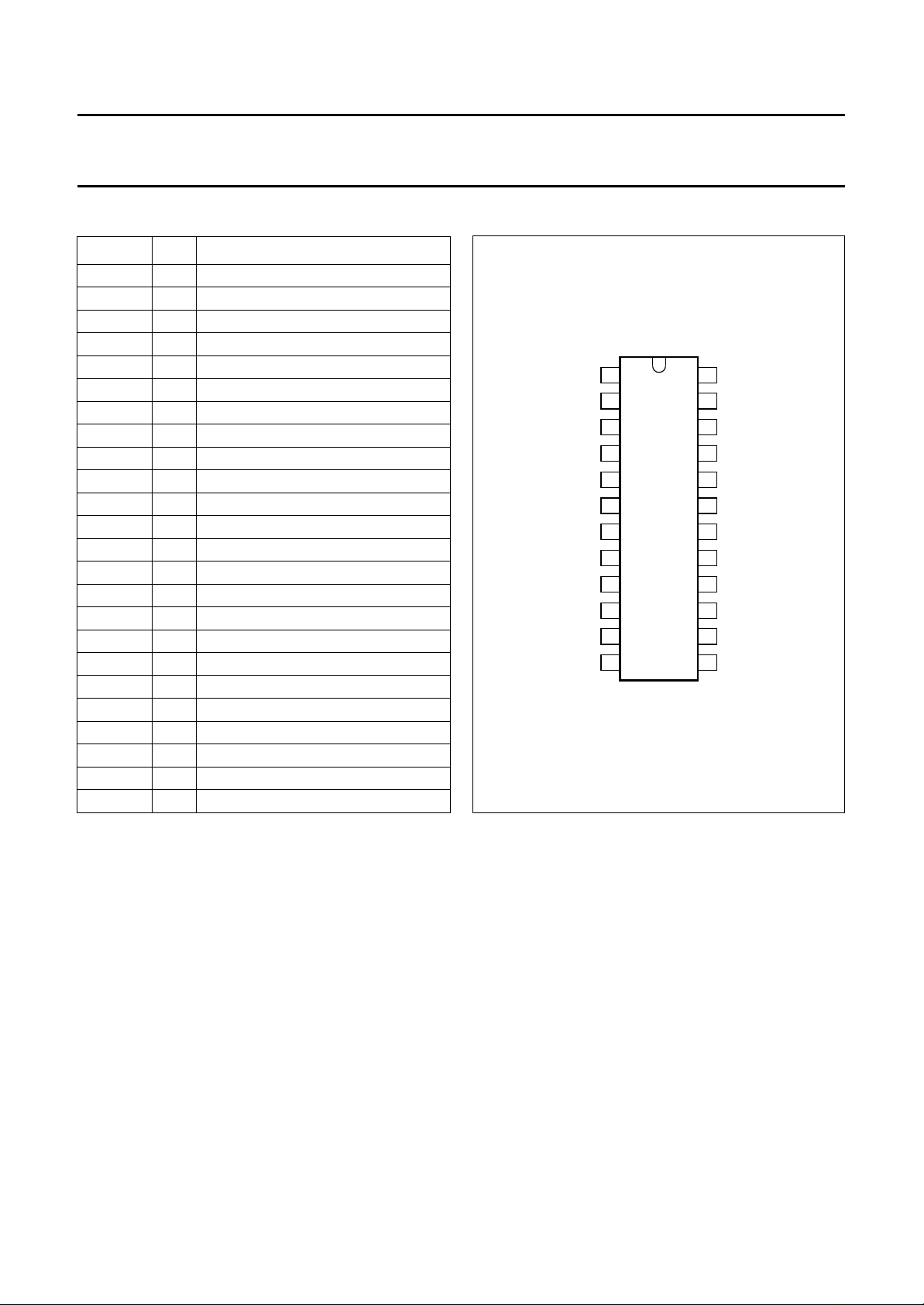
ORDERING INFORMATION
TYPE
NUMBER
TEA0675 SDIP24
TEA0675T SO24 plastic small outline package; 24 leads; body width 7.5 mm SOT137-1
Remark Dolby*: Available only to licensees of Dolby Laboratories Licensing Corporation, San Francisco, CA94111,
USA, from whom licensing and application information must be obtained. Dolby is a registered trade-mark of Dolby
Laboratories Licensing Corporation.
supply voltage 7.6 − 12 V
supply current − 26 31 mA
signal plus noise-to-noise ratio 78 84 − dB
PACKAGE
NAME DESCRIPTION VERSION
plastic shrink dual in-line package; 24 leads (400 mil)
SOT234-1
1996 Jun 07 2
Philips Semiconductors Preliminary specification
Dual Dolby* B-type noise reduction circuit
for playback applications
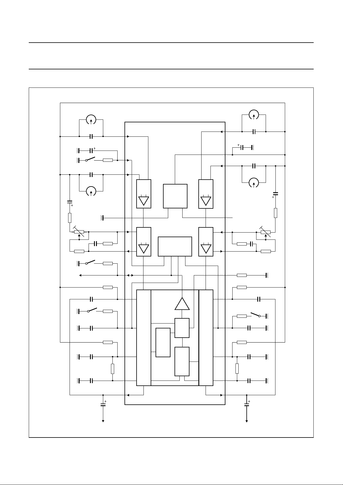
BLOCK DIAGRAM
pF
470
10
µF
27
kΩ
21
input
headswitch
10 µF
180 Ω
pF
470
PRE
1 kΩ
TEA0675
AMP.
POWER
TEA0675
MED621
pF
470
µF
100
pF
470
PRE
AMP.
SUPPL Y
CC
V
10 µF
180 Ω
1 kΩ
handbook, full pagewidth
AMS
330
output
kΩ
EQ
NR
4.7
15
100
330
70
120
10
nF
nF
nF
nF
nF
kΩ
8.2
µs
18
kΩ
µs
24
kΩ
kΩ
1.5
OFF ON
kΩ
180
270 kΩ
EQ
AMP.
LOGIC
AMS
PROCESSOR
TIME
DELA Y
DOLBY B
24 23 22 21 20 19 18 17 16 15 14 13
RISE TIME
LATCH AND
LEVEL
DETECTOR
EQ
AMP.
DOLBY B
789 1011 12
270 kΩ
12 3 4 5 6
kΩ
8.2
t
R
24
kΩ
kΩ
1.5
kΩ
180
100
330
10
nF
kΩ
330
nF
4.7
(1)
OFFON
AMS
15
nF
nF
nF
Fig.1 Block and application diagram.
for AMS-scan mode.
CC
10 µF
output B
1996 Jun 07 3
10 µF
output A
(1) Switched to V
Philips Semiconductors Preliminary specification
Dual Dolby* B-type noise reduction circuit
for playback applications
PINNING
SYMBOL PIN DESCRIPTION
OUTA 1 output channel A
INTA 2 integrating filter channel A
CONTRA 3 control voltage channel A
HPA 4 high-pass filter channel A
SCA 5 side chain channel A
TD 6 delay time constant
EQA 7 equalizing output channel A
EQFA 8 equalizing input channel A
V
CC
INA1 10 input channel A1 (forward or reverse)
V
ref
INA2 12 input channel A2 (reverse or forward)
INB2 13 input channel B2 (reverse or forward)
HS 14 head switch input
INB1 15 input channel B1 (forward or reverse)
GND 16 ground
EQFB 17 equalizing input channel B
EQB 18 equalizing output channel B
AMSEQ 19 AMS output and EQ switch input
SCB 20 side chain channel B
HPB 21 high-pass filter channel B
CONTRB 22 control voltage channel B
INTB 23 integrating filter channel B
OUTB 24 output channel B
9 supply voltage
11 reference voltage
handbook, halfpage
OUTA
1
INTA
2
CONTRA
HPA
SCA
TD
EQA
EQFA
V
CC
INA1
V
ref
INA2
3
4
5
6
7
8
9
10
11
12
TEA0675
Fig.2 Pin configuration.
MED622
TEA0675
OUTB
24
INTB
23
CONTRB
22
HPB
21
SCB
20
19
AMSEQ
EQB
18
17
EQFB
GND
16
INB1
15
HS
14
INB2
13
1996 Jun 07 4

Philips Semiconductors Preliminary specification
Dual Dolby* B-type noise reduction circuit
for playback applications
FUNCTIONAL DESCRIPTION
Noise Reduction (NR) is enabled when pin HPB is
open-circuit and disabled when connected to GND via an
1.5 kΩ resistor.
Dolby B noise reduction only operates correctly if 0 dB
Dolby level is adjusted at 387.5 mV.
Automatic Music Search (AMS) scan mode is enabled
when pin HPA is connected to VCC via an 1.5 kΩ resistor
and disabled when pin HPA is open-circuit. Switching AMS
on, internally NR is switched OFF simultaneously
(see Figs 5 and 6 for principle timing in AMS-scan mode).
AMS-latch mode is enabled when pin HPA is connected
to GND via an 1.5 kΩ resistor and disabled when pin HPA
is open-circuit. Switching AMS on, NR is switched off
internally. In this mode the device detects a pause level
signal, when a music level signal has appeared first
(see Figs 7 and 8 for principle timing). Furthermore a
longer rise time constant is supplied for suppressing the
detection of plops on tape. The output signal at pin
AMSEQ in this mode may be applied to drive a tape driver
logic circuit.
TEA0675
Equalization time constant switching (70 µs or 120 µs)
is achieved when pin AMSEQ is connected to GND via an
18 kΩ resistor (120 µs), or left open-circuit (70 µs).
This does not affect the AMS output signal during AMS
mode (see Fig.1).
Head switching is achieved when pin HS is connected
(input IN2 active) to GND via a 27 kΩ resistor, or left
open-circuit (input IN1 active). The 10 µF capacitor at pin
HS sets the time constants for smooth switching.
In AMS mode the signals of both channels are rectified and
then added. This means, even if one channel signal
appears inverted to the other channel, the normal AMS
function is ensured. Pins HPB and HPA perform the
function of a logic input for AMS, respectively NR mode
switching in both channels and provide the frequency
dependent feedback of the control chain amplifier in the
corresponding channel. Thus it is important that no voltage
is applied to pins HPB and HPA during NR on/AMS off
mode, otherwise this will cause irregular NR
characteristics.
LIMITING VALUES
In accordance with the Absolute Maximum Rating System (IEC 134).
SYMBOL PARAMETER CONDITIONS MIN. MAX. UNIT
V
CC
V
i
t
short
T
stg
T
amb
V
es
supply voltage 0 14 V
input voltage (except pin 11) −0.3 +V
pin 11 (V
) to VCC short-circuiting duration − 5s
ref
CC
V
storage temperature −55 +150 °C
operating ambient temperature −40 +85 °C
electrostatic handling voltage for all pins note 1 −2+2kV
note 2 −500 +500 V
Notes
1. Human body model (1.5 kΩ, 100 pF).
2. Machine model (0 Ω, 200 pF).
1996 Jun 07 5

Philips Semiconductors Preliminary specification
Dual Dolby* B-type noise reduction circuit
TEA0675
for playback applications
CHARACTERISTICS
VCC= 10 V; f = 20 Hz to 20 kHz; T
pin OUTA or OUTB; see Fig.1; NR on/AMS off; EQ switch in the 70 µs position; unless otherwise specified.
SYMBOL PARAMETER CONDITIONS MIN. TYP. MAX. UNIT
V
CC
I
CC
α
m
supply voltage 7.6 10 12 V
supply current − 26 31 mA
channel matching f = 1 kHz; Vo= 0 dB; NR off −0.5 − +0.5 dB
THD total harmonic distortion
(2nd and 3rd harmonic)
H
R
SN+
-------------N
headroom at output VCC= 7.6 V; THD = 1%;
signal plus noise-to-noise
ratio
PSRR power supply ripple
rejection
f
o
frequency response;
referenced to TP
α
cs
α
cc
channel separation Vo= 10 dB; f = 1 kHz;
crosstalk between active
and inactive input
R
L
G
v
load resistance at output AC-coupled; f = 1 kHz;
voltage gain of
pre-amplifier
V
I(offset)(DC)
I
i(bias)
R
EQ
R
i
DC input offset voltage − 2 − mV
input bias current − 0.1 0.4 µA
equalization resistor 4.7 5.8 6.9 kΩ
input resistance head
inputs
A
v
open-loop amplification pin INA1 or
=25°C; all levels are referenced to 387.5 mV (RMS) (0 dB) at test point (TP)
amb
f = 1 kHz; V
f = 10 kHz; V
=0dB − 0.08 0.15 %
o
=10dB − 0.15 0.3 %
o
12 −− dB
f = 1 kHz
internal gain 40 dB, linear;
78 84 − dB
CCIR/ARM weighted;
decode mode; see Fig.25
= 0.25 V; f = 1 kHz;
V
i(rms)
52 57 − dB
see Fig.22
encode mode; see Fig.25
= −25 dB; f = 0.2 kHz −22.9 −24.4 −25.9 dB
V
o
= 0 dB; f = 1 kHz −1.5 0 +1.5 dB
V
o
= −25 dB; f=1kHz −17.8 −19.3 −20.8 dB
V
o
= −25 dB; f=5kHz −18.1 −19.6 −21.1 dB
V
o
= −35 dB; f = 10 kHz −24.4 −25.9 −27.4 dB
V
o
57 63 − dB
see Fig.23
f = 1 kHz; Vo= 10 dB;
70 77 − dB
NR off; see Fig.23
10 −− kΩ
Vo= 12 dB; THD = 1%
from pin INA1 or INA2 to
29 30 31 dB
pin EQFA and from
pin INB1 or
INB2 to pin EQFB;
f = 1 kHz
60 100 − kΩ
INA2 to pin EQA and
pin INB1 or INB2 to
pin EQB
f = 10 kHz 80 86 − dB
f = 400 Hz 104 110 − dB
1996 Jun 07 6

Philips Semiconductors Preliminary specification
Dual Dolby* B-type noise reduction circuit
TEA0675
for playback applications
SYMBOL PARAMETER CONDITIONS MIN. TYP. MAX. UNIT
V
− V
ref
I
O
Z
o
V
no(rms)
V
TD
EMC DC offset voltage at
Switching thresholds
V
NROFF
I
NROFF
I
NRON
V
HPB(max)
HPA (PIN 4)
V
AMSlON
I
AMSlON
V
AMSsON
I
AMSsON
I
AMSOFF
V
HPA(max)
AMSEQ (PIN 19)
DC output offset voltage
OUT
at pins OUTA and OUTB
NR off; pins INA1, INA2,
INB1 and INB2 connected
to V
ref
−0.15 − +0.15 V
DC output current pin OUTA to ground −2 −− mA
pin OUTB to V
CC
0.3 −− mA
output impedance − 80 100 Ω
equivalent input noise
voltage (RMS value)
AMS timing (DC level) resistor Rt connected to
NR off; unweighted;
f = 20 Hz to 20 kHz;
R
source
=0Ω
− 0.7 1.4 µV
VCC− 3 − V
CC
V
pin TD
i(rms)
=6V;
pins OUTA and OUTB
f = 900 MHz; V
see Figs 26, 27 and 28
voltage at HPB (pin 21) NR off 0.19V
− 40 − mV
CC
0.23V
CC
0.25V
CC
V
output current NR off −−0.7 −1mA
input current NR on − open 200 nA
maximum voltage −−0.75V
pin voltage AMS-latch on 0.19V
CC
0.23V
CC
0.25V
CC
CC
V
V
output current −−0.7 −1mA
pin voltage AMS-scan on 0.75V
CC
0.77V
CC
0.81V
CC
V
input current − 0.8 1 mA
pin current AMS off − open 200 nA
maximum voltage −−0.75V
CC
V
AMS output (AMS mode)
V
OH
I
OH1
I
OH2
t
d
HIGH level output voltage 4 4.6 5 V
HIGH level output current note 1 +10 −−150 µA
HIGH level output current note 1 +0.01 −−1mA
minimum pulse width;
see Table 1 − 23 to 160 − ms
delay time range
V
OL
I
OL
t
r
A
M/P
LOW level output voltage − 0.1 0.7 V
LOW level output current −0.02 − +1 mA
minimum pulse width rise
time
signal level at output for
AMS switching
AMS-scan mode 2 6 10 ms
AMS-latch mode 130 150 170 ms
AMS mode; f = 10 kHz;
note 2; see Fig.24
music to pause
1996 Jun 07 7
−25 −22 −19 dB

Philips Semiconductors Preliminary specification
Dual Dolby* B-type noise reduction circuit
TEA0675
for playback applications
SYMBOL PARAMETER CONDITIONS MIN. TYP. MAX. UNIT
A
P/M
EQ switch input (not AMS mode)
I
EQ70
I
EQ120
I
EQth
HEAD SWITCHING
V
HSW
I
HSW
V
HSW(HIGH)
V
HSW(LOW)
Notes
1. In AMS off mode, pin AMSEQ is HIGH level, the equalization time constant will be switched by pulling approximately
200 µA out of pin AMSEQ. This means for the device connected to pin AMSEQ, a restriction of input current at HIGH
level less than 200 µA during AMS off; otherwise the selection of the equalization time constant is disabled and fixed
at 120 µs. If the connected devices consume more than 200 µA, this input has to be disconnected in AMS off mode.
(To ensure switching, the currents for the different switched modes are specified with a tolerance of ±50 µA in
Chapter “Characteristics”.) For an application with a fixed EQ time constant of 120 µs the equalizing network may be
applied completely external. Change 8.2 kΩ resistor to 14 kΩ the internal resistor REQ= 5.8 kΩ is short-circuited by
fixing the EQ switch input at the 70 µs position (I
2. The high speed of the tape (FF, REW) at the tape head during AMS mode causes a transformation of level and
frequency of the originally recorded signal. It means a boost of signal level of approximately 10 dB and more for
recorded frequencies from 500 Hz up to 4 kHz. So the threshold level of −22 dB corresponds to signal levels in Play
Back (PB) mode of approximately −32 dB. The AMS inputs for each channel are pin SCA and pin SCB. As the
frequency spectrum is transformed by a factor of approximately 10 to 30 due to the higher tape speed in FF, REW,
the high-pass filter (4.7 nF/24 kΩ) removes the effect of offset voltages but does not affect the music search function.
In the application circuit (Fig.1) the frequency response of the system between tape heads input, e.g. pins INA2 and
INB2, to the AMS input pins SCA and SCB is constant over the whole frequency range (see Fig.3).
3. To activate the inputs IN1, pin HS might be left open-circuit. In this event the DC level at pin HS is 0.775VCC.
signal level at output for
AMS mode; f = 10 kHz; −24 −21 −18 dB
AMS switching
pause to music
input current time constant 70 µs active −150 −− µA
input voltage time constant 120 µs active −1000 −−250 µA
threshold current note 1 −−200 −µA
pin voltage load current +90 to −90 µA − 0.8V
input current V
HIGH level pin voltage inputs INA1 and INB1
HSW
=0toV
CC
−170 − +170 µA
1
⁄2VCC+ 0.5 − V
− V
CC
CC
V
active; note 3
LOW level pin voltage inputs INA2 and INB2
0 −
1
⁄2VCC− 0.5 V
active
).
EQ70
1996 Jun 07 8
Philips Semiconductors Preliminary specification
Dual Dolby* B-type noise reduction circuit
for playback applications
Table 1 Blank delay time set by resistor Rt at pin TD
RESISTOR VALUE R
t
(kΩ)
68 23 20
150 42 15
180 48 15
220 56 15
270 65 10
330 76 10
470 98 10
560 112 10
680 126 10
820 142 10
1000 160 10
General note
It is recommended to switch off V
with a gradient of 400 V/s at maximum to avoid plops on tape in the event of contact
CC
between tape and tape head while switching off.
DELAY TIME t
TYP. (ms)
TEA0675
d
TOLERANCE
(%)
−20
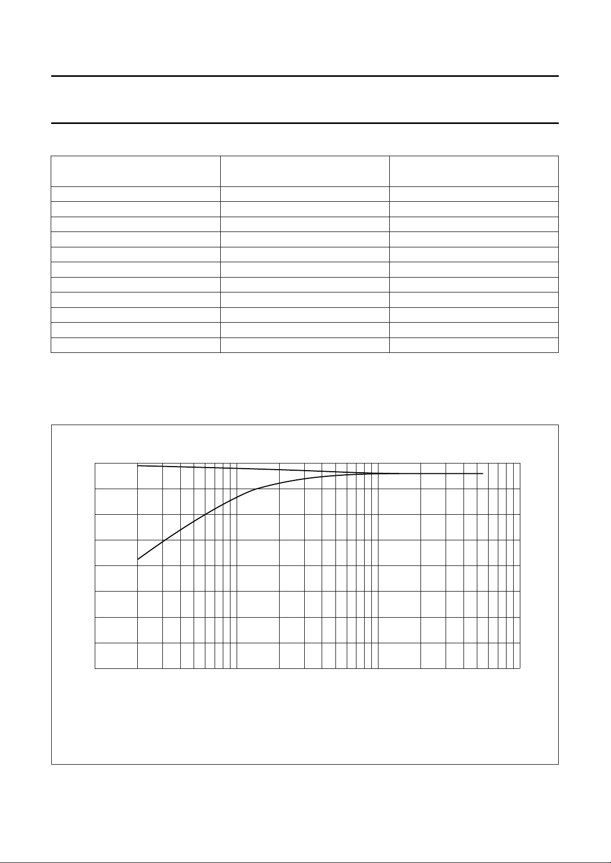
handbook, full pagewidth
(dB)
−30
−40
−50
−60
2
10
(1) AMS threshold level for application circuit (Fig.1).
(2) AMS threshold level for test circuit (Fig.24).
(1)
(2)
3
10
Fig.3 AMS threshold level.
MED623
4
10
(Hz)
5
10
1996 Jun 07 9
Philips Semiconductors Preliminary specification
Dual Dolby* B-type noise reduction circuit
for playback applications
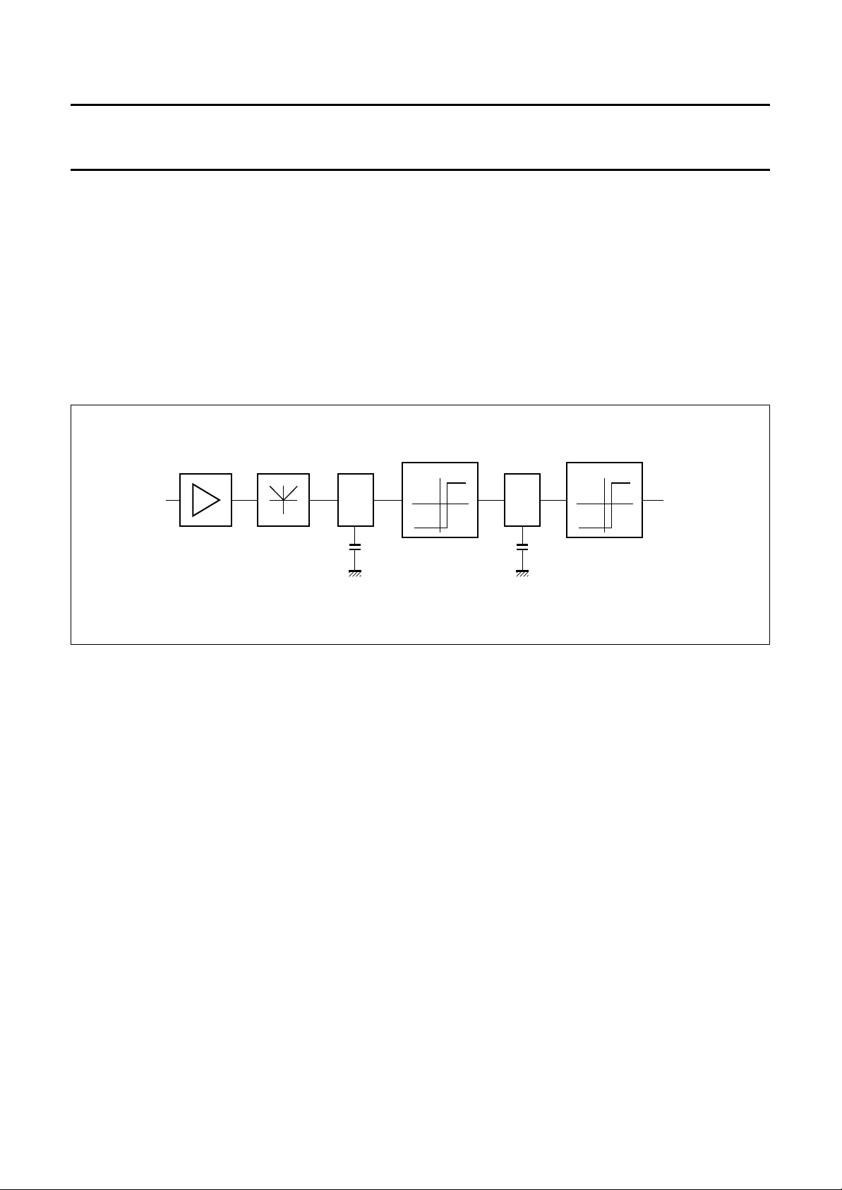
Short description ‘music search’
A system for ‘music search’ mainly consists of a level and
a time detection (see Fig.4). For adapting and decoupling
the input signal will be amplified (A), then rectified (B) and
smoothed with a time constant (C). So the voltage at (C)
corresponds to the signal level and will be compared to the
predefined pause level at the first comparator (D), the level
detector. If the signal level becomes smaller than the
pause level, the level detector changes its output signal.
Due to the output level of the level detector the capacitor
of the second time constant (E) will be charged,
handbook, full pagewidth
INPUT
(A)
(B)
(C)
COMPARATOR 1 COMPARATOR 2
V
I
t
1
TEA0675
respectively discharged. If the pause level of the input
signal remains for a certain time, the voltage at the
capacitor reaches a certain value, which corresponds to
an equivalent time value. The voltage at the capacitor will
be compared to a predefined time-equivalent voltage by
the second comparator (F), the time detector. If the pause
level of the input signal remains for this predefined time,
the time detector changes its output level for ‘pause found’
status.
(D)
(E) (F)
V
t
t
2
OUTPUT
AMPLIFIER RECTIFIER
LEVEL DETECTOR TIME DETECTOR
MED624
Fig.4 Integrated ‘music search’ function.
1996 Jun 07 10
 Loading...