

Philips tea0665 DATASHEETS

INTEGRATED CIRCUITS
DATA SH EET
TEA0665
TEA0665T
Dolby B and C type noise reduction
circuit
Product specification
File under Integrated Circuits, IC01
May 1992

Philips Semiconductors Product specification
Dolby B and C type noise reduction
circuit
GENERAL DESCRIPTION
The TEA0665 is designed for use in Dolby
provides the high and low level stages for one channel of a Dolby C-type NR system, including NR ON/OFF switching
and all electronic switching necessary for Dolby C-type systems. In addition the TEA0665 includes a preamplifier for the
record and playback functions and a multiplex buffer amplifier. The circuit offers two different line-output levels (−6 and
0 dBm) and a low-pass filter, which can be fed into the signal path in playback mode.
Features
• Few external components required
• Included RECORD/PLAY preamplifiers plus multiplex filter buffer amplifier
• Two different line-output levels
• All electronic switching
PACKAGE OUTLINES
TEA0665: 28-lead DIL; plastic (SOT117); SOT117-1; 1996 September 9.
TEA0665T: 28-lead mini-pack; plastic (SO28; SOT136A); SOT136-1; 1996 September 9.
(1)
B and Dolby C type audio Noise Reduction (NR) systems. The device
TEA0665
TEA0665T
(1) Available only to licensees of Dolby Laboratories Licensing Corporation, San Francisco, CA94111 U.S.A., from
whom licensing and application information must be obtained. Dolby is a registered trademark of Dolby
Laboratories Licensing Corporation.
May 1992 2
Philips Semiconductors Product specification
Dolby B and C type noise reduction circuit
TEA0665
TEA0665T
May 1992 3
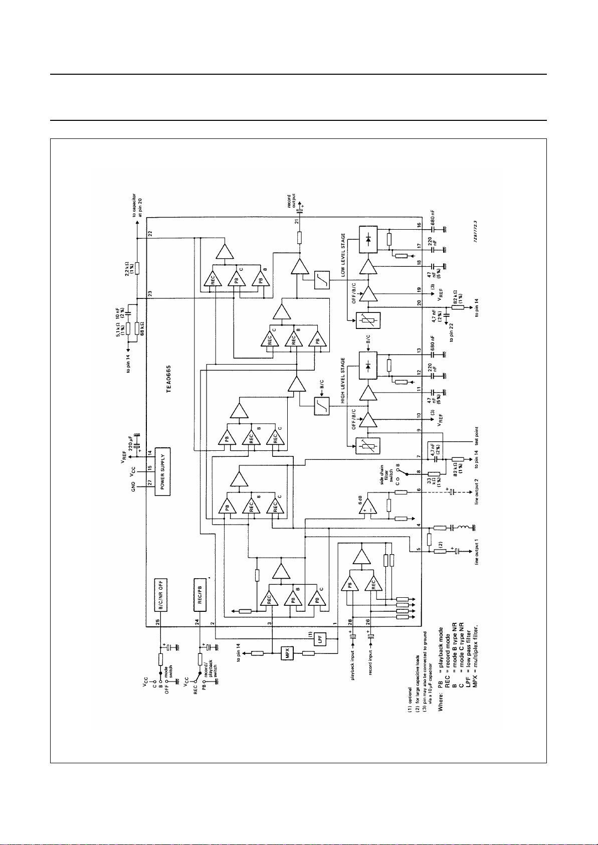
Fig.1 Block diagram and application circuit.
Philips Semiconductors Product specification
Dolby B and C type noise reduction circuit
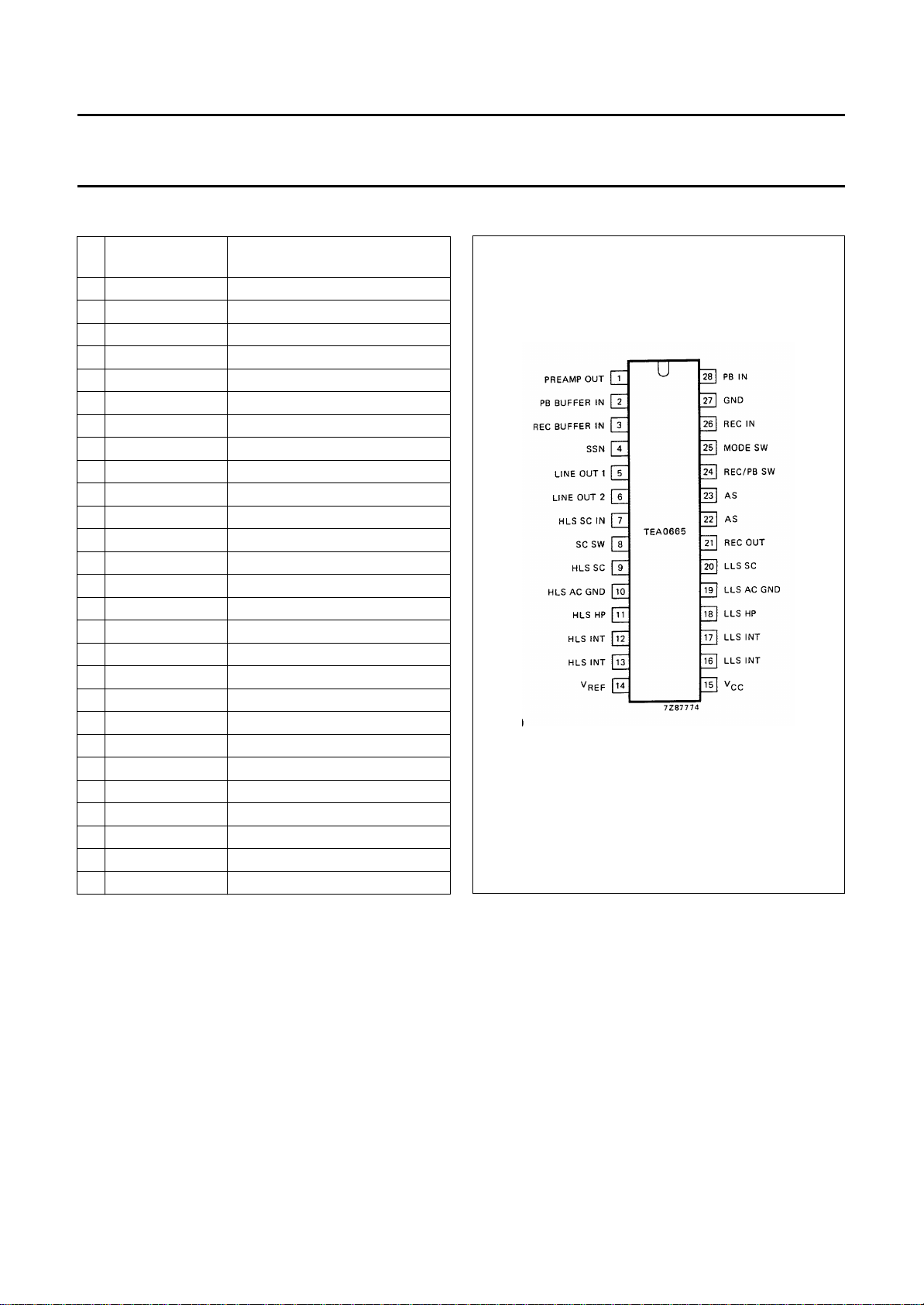
PINNING
1 PREAMP OUT record/playback preamplifier
output
2 PB BUFFER IN play back amplifier input buffer
3 REC BUFFER IN record amplifier input buffer
4 SSN spectral skewing network
5 LINE OUT 1 line output 1
6 LINE OUT 2 line output 2
7 HLS SC IN high level stage side chain input
8 SC SW side chain filter switch
9 HLC SC high level stage side chain
10 HLS AC GND high level stage AC ground
11 HLS HP high level stage high pass filter
12 HLS INT high level stage integrating filter
13 HLS INT high level stage integrating filter
14 V
REF
15 V
CC
16 LLS INT low level stage integrating filter
17 LLS INT low level stage integrating filter
18 LLS HP low level stage high pass filter
19 LLS AC GND low level stage AC ground
20 LLS SC low level stage side chain
21 REC OUT record output
22 AS anti-saturation filter
23 AS anti-saturation filter
24 REC/PB SW record/playback switch input
25 MODE SW mode switch input
26 REC IN record input
27 GND ground
28 PB IN playback input
reference voltage
positive supply voltage
TEA0665
TEA0665T
Fig.2 Pinning diagram.
RATINGS
Limiting values in accordance with the Absolute Maximum System (IEC 134)
Supply voltage (pin 15) V
Input voltage (pins 26 and 28) V
Total power dissipation P
Storage temperature range T
Operating ambient temperature range T
May 1992 4
max. 18 V
CC
max.−0,3 to VCCV
I
tot
stg
amb
−55 to + 150 °C
−40 to + 85 °C
600 mW

Philips Semiconductors Product specification
Dolby B and C type noise reduction circuit
TEA0665
TEA0665T
CHARACTERISTICS
= 14 V; f = 20 Hz to 15 kHz; T
V
CC
test circuit Fig.5; record mode; unless otherwise specified.
PARAMETER
Supply
Supply voltage range C − note 1
single V
(split) V
Supply current OFF − no input
Input sensitivity C note 2
of record amplifier pin 26 V
of playback amplifier pin 28 V
Signal handling C 1 V
of record output THD = 1% 12 15 − dB
(note 3; see Fig.8) 1 V
Line output 1 note 3 −0,5 0 +0,5 dB
Line output 2;
amplifier gain V
o/Vi
(pin 6 to pin 5)
Total harmonic
distortion OFF 1 TPL = 0 dB
Total harmonic
distortion B 1 TPL = 0 dB THD − 0,1 0,15 %
Total harmonic
distortion C 1 TPL 0 dB THD − 0,15 0,3 %
Signal plus noise- C R
to-noise ratio CCIR/ARM
= 25 °C; all levels with reference to 387,5 mV = 0 dB = −6 dBm at test point pin 7;
amb
CONDITIONS
SYMBOL MIN. TYP. MAX. UNIT
MODE F (KHZ)
8 1416V
(±4) (±7) (±8) V
− 17 25 mA
43 50 57 mV
25 30 35 mV
signal I
= 8 V
CC
= 14 V
CC
CC
CC
CC
i
i
THD = 1% − 20 − dB
(6)
G
v
THD − 0,02 0,1 %
+5,5 +6 +6,5 dB
TPL = + 10 dB THD − 0,05 0,3 %
TPL = + 10 dB THD − 0,08 0,3 %
10 TPL = 0 dB THD − 0,06 0,1 %
TPL + 10 dB THD − 0,13 0,5 %
= 10 kΩ
S
weighted (S+N)/N 62 66 − dB
May 1992 5
 Loading...