

Philips tea0655 DATASHEETS

INTEGRATED CIRCUITS
DATA SH EET
TEA0655
Dual Dolby B-type noise reduction
circuit for playback applications
Product specification
File under Integrated Circuits, IC01
September 1990

Philips Semiconductors Product specification
Dual Dolby B-type noise reduction
TEA0655
circuit for playback applications
GENERAL DESCRIPTION
The TEA0655 is an integrated circuit that provides two Dolby* B-type noise reduction channels for playback applications
in car radios. The TEA0655 includes head and equalization amplifiers with electronically switched time constants.
The device will operate with power supplies in the range 9 to 15 volts, the output overload level increasing with an
increase in supply voltage. Current drain varies with supply voltage and noise reduction ON/OFF, therefore it is advisable
to use a regulated power supply or a supply with a long time constant.
FEATURES
• Dual noise reduction channels
• Head preamplifiers
• Equalization with electronically switched time constants
• Dolby reference level = 387.5 mV.
QUICK REFERENCE DATA
SYMBOL PARAMETER MIN. TYP. MAX. UNIT
V
CC
I
CC
(S+N)/N signal plus noise-to-noise ratio 78 84 − dB
supply voltage range 8 − 15 V
supply current − 20 25 mA
ORDERING AND PACKAGE INFORMATION
EXTENDED TYPE
NUMBER
TEA0655 20 DIL plastic SOT146 **
* Available only to licensees of Dolby Laboratories Licensing Corporation, San Francisco, CA94111, USA, from whom
licensing and application information must be obtained. Dolby is a registered trade-mark of Dolby Laboratories
Licensing Corporation.
** SOT146-1, August 1996.
PINS PIN POSITION MATERIAL CODE
PACKAGE
September 1990 2
Philips Semiconductors Product specification
Dual Dolby B-type noise reduction circuit
for playback applications
TEA0655
September 1990 3
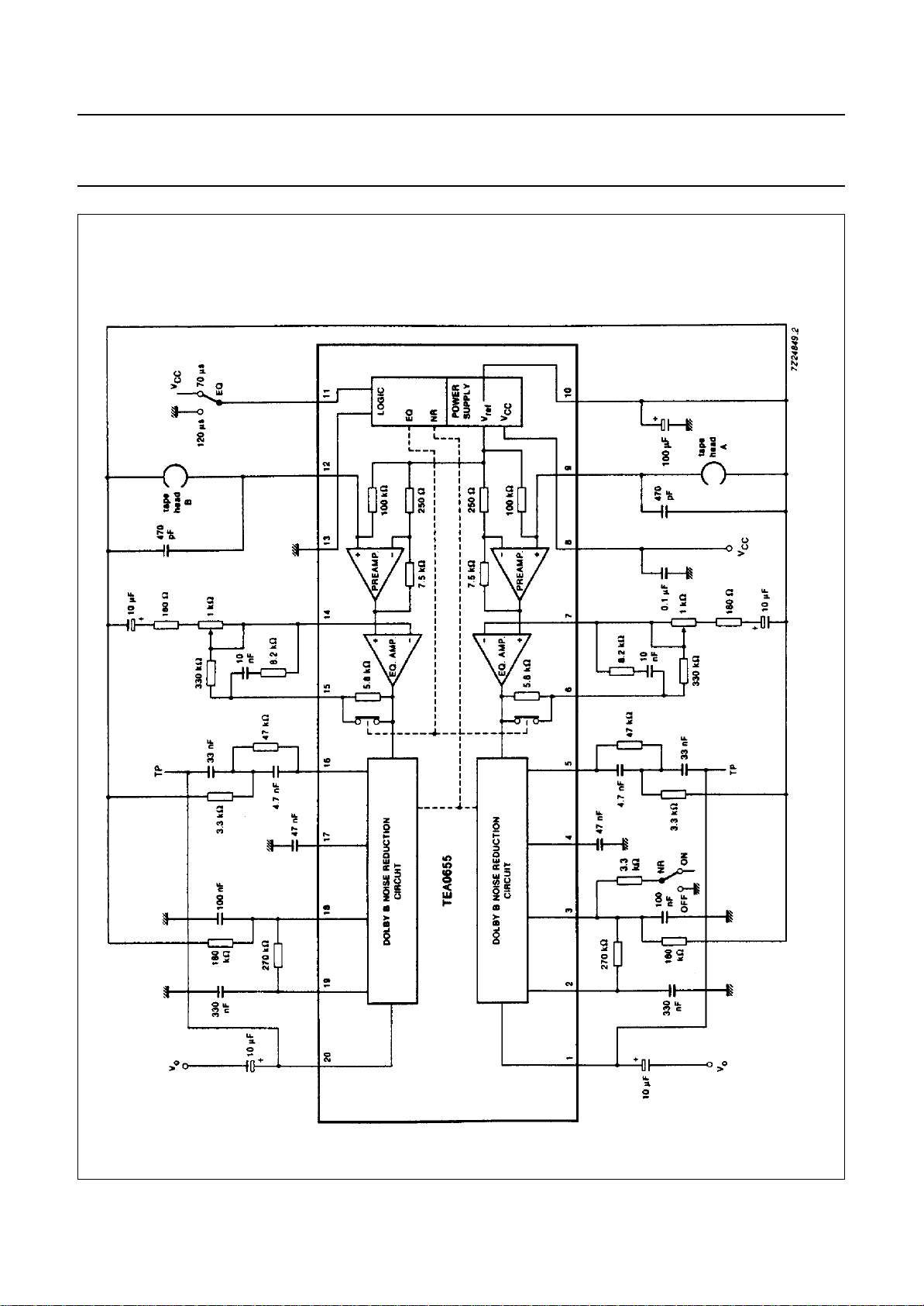
Fig.1 Block and application diagram.

Philips Semiconductors Product specification
Dual Dolby B-type noise reduction circuit
TEA0655
for playback applications
FUNCTIONAL DESCRIPTION
Noise reduction is enabled when pin 3 is open-circuit and disabled when pin 3 is connected to GRD (pin 13) via a 3.3 kΩ
resistor (see Fig.1).
Pin 3 performs the functions of a logic input for noise reduction switching for both channels. It also provides smoothing
for the control signal in one channel. It is important that no voltage is applied to pin 3 when in the NR ON mode as this
will cause irregular noise reduction characteristics in the selected channel. Time constant switching is achieved by
applying a DC voltage to pin 11.
PINNING
SYMBOL PIN DESCRIPTION
OUTA 1 output channel A
INTA 2 integrating filter channel A
CONTRA 3 control voltage channel A
HPA 4 high-pass filter channel A
SCA 5 side chain channel A
EQA 6 equalizing output channel A
EQFA 7 equalizing input channel A
V
CC
INA 9 input channel A
V
ref
SWEQ 11 equalizing switch
INB 12 input channel B
GRD 13 ground
EQFB 14 equalizing input channel B
EQB 15 equalizing output channel B
SCB 16 side chain channel B
HPB 17 high-pass filter channel B
CONTRB 18 control voltage channel B
INTB 19 integrating filter channel B
OUTB 20 output channel B
8 voltage supply
10 reference voltage
LIMITING VALUES
Limiting values in accordance with the Absolute Maximum Rating System (IEC 134)
SYMBOL PARAMETER MIN. MAX. UNIT
V
V
T
T
V
CC
I
amb
stg
es
supply voltage − 16 V
input voltage (pins 1 to 20) −0.3 V
operating ambient temperature range −40 +85 °C
storage temperature range −65 +150 °C
electrostatic handling
* Classification A: human body model; C = 100 pF, R = 1.5 kΩ, V = ≥ 2 kV; charge device model; C = 200 pF, R = 0 Ω,
V ≥ 500 V.
September 1990 4
CC
*
−−−
V
 Loading...