

Page 1

Colour Television Chassis
TE3.1E
CA
Contents Page Contents Page
1. Technical Specifications, Connections and Chassis
Overview 2
2. Safety Instructions, Warnings, and Notes 4
3. Directions for Use 6
4. Mechanical Instructions 7
5. Service Modes, Error Codes and Fault Finding 8
6. Block Diagrams, Test Point Overviews, and
Waveforms
Wiring Diagram 11
Block Diagram Main 12
Block Diagram Power Supply 13
I2C Diagram 14
7. Circuit Diagrams and PWB Layouts Diagram PWB
Main Panel: Tuner (A1) 15 24-25
Main Panel: EEPROM and MCU (A2 - A6) 16 24-25
Main Panel: Sound (A3) 17 24-25
Main Panel: Deflection (A4 - A10) 18 24-25
Main Panel: Video (A5) 19 24-25
Side AV Panel (A7) 20 26Main Panel: Power (A8) 21 24-25
Main Panel: Scart (A9) 22 24-25
Main Panel: CRT (A11) 23 24-25
8. Electrical Alignments 27
9. Circuit Description and Abbreviation List 30
10. SpareParts List 40
11. Revision List 43
©
Copyright 2005 Philips Consumer Electronics B.V. Eindhoven, The Netherlands.
All rights reserved. No part of this publication may be reproduced, stored in a
retrieval system or transmitted, in any form or by any means, electronic,
mechanical, photocopying, or otherwise without the prior permission of Philips.
Published by JH 0568 Service PaCE Printed in the Netherlands Subject to modification EN 3122 785 15850
Page 2

EN 2 TE3.1E CA1.
Technical Specifications, Connections and Chassis Overview
1. Technical Specifications, Connections and Chassis Overview
1.1 Technical Specifications
Index of this chapter:
1.1 Technical Specifications
1.2 Connections / Control Facilities
1.3 Chassis Overview
Notes:
• Figures can deviate due to the different set executions.
• Specifications are indicative (subject to change).
1.1.1 Reception
Tuning system : PLL
Colour systems : PAL B/G, D/K, I
: SECAM B/G, L/L'
Sound systems : FM/FM (5.5 - 5.74)
(B/G)
: NICAM B/G
(5.5 - 5.85),
NICAM D/K
: NICAM I (6.0 - 6.52),
NICAM L (6.5 (AM) -
5.85)
A/V connections : NTSC 3.58
: NTSC 4.43
Channel selections : 100 channels
: UVSH
IF frequency : 38.9 MHz
Aerial input : 75 :, Coax
Audio / Video In
1 -Video CVBS (1 Vpp / 75 :) jq
2 -Audio L (0.5 Vrms / 10 k:) jq
3 -Audio R (0.5 Vrms / 10 k:) jq
4 -Headphone 3.5 mm (8 - 600 : /
<100 mW) rt
1.2.2 Rear Connections
75 Ohm
EXT1
Figure 1-3 Rear Connections
TV Aerial In
Aerial input : 75 :, Coax
(IEC-type)
External 1: RGB in + CVBS in/out
20
2
F_15850_002.eps
160805
1.1.2 Miscellaneous
Audio output (RMS) : 2 x 3 W stereo
Mains voltage : 220 - 240V
Mains frequency : 50 / 60 Hz (r 5 %)
Ambient temperature : + 5 to + 45 deg. C
Maximum humidity : 90%
Power consumption : 55W r 10%
Standby Power consumption : < 3W
1.2 Connections / Control Facilities
1.2.1 Side Connections and Front Control
-
+
SK1
IR - VOLUME +
LIGHT SENSOR LENS
RED
Figure 1-1 Front Control
Video
- PROGRAM +
Audio
R
L
F_15850_001.eps
160805
21
E_06532_001.eps
1
050404
Figure 1-4 SCART connector
1 -Audio R (0.5 Vrms 1 k:) k
2 -Audio R (0.5 Vrms 10 k:) j
3 -Audio L (0.5 Vrms 1 k:) k
4 - GND H
5 - GND H
6 -Audio L (0.5 Vrms 10 k:) j
7 -Blue (0.7 Vpp / 75 :) j
8 -CVBS-status 0 - 2.0 V: INT
4.5 - 12 V: EXT 4:3
9 - GND H
10 -
11 - Green (0.7 Vpp / 75 :) j
12 -
13 - GND H
14 - GND H
15 - Red (0.7 Vpp / 75 :) j
16 - RGB-status 0 - 0.4 V: INT
1 - 3 V: EXT / 75 :
17 - GND H
18 - GND H
19 - CVBS (1 Vpp / 75 :) k
20 - CVBS (1 Vpp / 75 :) j
21 - Earth GND vj
F_15160_002.eps
040705
Figure 1-2 Side AV
Page 3
Technical Specifications, Connections and Chassis Overview
1.3 Chassis Overview
CRT PANEL
A11
EN 3TE3.1E CA 1.
SIDE AV PANEL
A7
Figure 1-5 Chassis Overview
MAIN
CHASSIS
PANEL
TUNER
EEPROM
AUDIO
VERTICAL
VIDEO PROCESSOR
µ-CONTROLLER
POWER BLOCK
SCART
HORIZONTAL
F_15850_003.eps
A1
A2
A3
A4
A5
A6
A8
A9
A10
160805
Page 4

EN 4 TE3.1E CA2.
Safety Instructions, Warnings, and Notes
2. Safety Instructions, Warnings, and Notes
Index of this chapter:
2.1 Safety Instructions
2.2 Warnings
2.3 Notes
2.1 Safety Instructions
Safety regulations require the following during a repair:
• Connect the set to the Mains (AC Power) via an isolation
transformer (> 800 VA).
• Replace safety components, indicated by the symbol h,
only by components identical to the original ones. Any
other component substitution (other than original type) may
increase risk of fire or electrical shock hazard.
Safety regulations require that after a repair, the set must be
returned in its original condition. Pay in particular attention to
the following points:
• Route the wire trees correctly and fix them with the
mounted cable clamps.
• Check the insulation of the Mains (AC Power) lead for
external damage.
• Check the strain relief of the Mains (AC Power) cord for
proper function.
• Check the electrical DC resistance between the Mains (AC
Power) plug and the secondary side (only for sets that have
a Mains (AC Power) isolated power supply):
1. Unplug the Mains (AC Power) cord and connect a wire
between the two pins of the Mains (AC Power) plug.
2. Set the Mains (AC Power) switch to the "on" position
(keep the Mains (AC Power) cord unplugged!).
3. Measure the resistance value between the pins of the
Mains (AC Power) plug and the metal shielding of the
tuner or the aerial connection on the set. The reading
should be between 4.5 Mohm and 12 Mohm.
4. Switch "off" the set, and remove the wire between the
two pins of the Mains (AC Power) plug.
• Check the cabinet for defects, to prevent touching of any
inner parts by the customer.
2.3 Notes
2.3.1 General
• Measure the voltages and waveforms with regard to the
chassis (= tuner) ground (H), or hot ground (I), depending
on the tested area of circuitry. The voltages and waveforms
shown in the diagrams are indicative. Measure them in the
Service Default Mode (see chapter 5) with a colour bar
signal and stereo sound (L: 3 kHz, R: 1 kHz unless stated
otherwise) and picture carrier at 475.25 MHz for PAL, or
61.25 MHz for NTSC (channel 3).
• Where necessary, measure the waveforms and voltages
with (D) and without (E) aerial signal. Measure the
voltages in the power supply section both in normal
operation (G) and in stand-by (F). These values are
indicated by means of the appropriate symbols.
• The semiconductors indicated in the circuit diagram and in
the parts lists, are interchangeable per position with the
semiconductors in the unit, irrespective of the type
indication on these semiconductors.
2.3.2 Schematic Notes
• All resistor values are in ohms, and the value multiplier is
often used to indicate the decimal point location (e.g. 2K2
indicates 2.2 kohm).
• Resistor values with no multiplier may be indicated with
either an "E" or an "R" (e.g. 220E or 220R indicates 220
ohm).
• All capacitor values are given in micro-farads (P x10
nano-farads (n= x10
• Capacitor values may also use the value multiplier as the
decimal point indication (e.g. 2p2 indicates 2.2 pF).
• An "asterisk" (*) indicates component usage varies. Refer
to the diversity tables for the correct values.
• The correct component values are listed in the Spare Parts
List. Therefore, always check this list when there is any
doubt.
-9
), or pico-farads (p= x10
-12
-6
),
).
2.2 Warnings
• All ICs and many other semiconductors are susceptible to
electrostatic discharges (ESD w). Careless handling
during repair can reduce life drastically. Make sure that,
during repair, you are connected with the same potential as
the mass of the set by a wristband with resistance. Keep
components and tools also at this same potential. Available
ESD protection equipment:
– Complete kit ESD3 (small tablemat, wristband,
connection box, extension cable and earth cable) 4822
310 10671.
– Wristband tester 4822 344 13999.
• Be careful during measurements in the high voltage
section.
• Never replace modules or other components while the unit
is switched "on".
• When you align the set, use plastic rather than metal tools.
This will prevent any short circuits and the danger of a
circuit becoming unstable.
2.3.3 Rework on BGA (Ball Grid Array) ICs
General
Although (LF)BGA assembly yields are very high, there may
still be a requirement for component rework. By rework, we
mean the process of removing the component from the PWB
and replacing it with a new component. If an (LF)BGA is
removed from a PWB, the solder balls of the component are
deformed drastically so the removed (LF)BGA has to be
discarded.
Device Removal
As is the case with any component that, is being removed, it is
essential when removing an (LF)BGA, that the board, tracks,
solder lands, or surrounding components are not damaged. To
remove an (LF)BGA, the board must be uniformly heated to a
temperature close to the reflow soldering temperature.
A uniform temperature reduces the risk of warping the PWB. To
do this, we recommend that the board is heated until it is certain
that all the joints are molten. Then carefully pull the component
off the board with a vacuum nozzle. For the appropriate
temperature profiles, see the IC data sheet.
Area Preparation
When the component has been removed, the vacant IC area
must be cleaned before replacing the (LF)BGA.
Removing an IC often leaves varying amounts of solder on the
mounting lands. This excessive solder can be removed with
either a solder sucker or solder wick. The remaining flux can be
removed with a brush and cleaning agent.
Page 5
Safety Instructions, Warnings, and Notes
EN 5TE3.1E CA 2.
After the board is properly cleaned and inspected, apply flux on
the solder lands and on the connection balls of the (LF)BGA.
Note: Do not apply solder paste, as this has been shown to
result in problems during re-soldering.
Device Replacement
The last step in the repair process is to solder the new
component on the board. Ideally, the (LF)BGA should be
aligned under a microscope or magnifying glass. If this is not
possible, try to align the (LF)BGA with any board markers.
So as not to damage neighbouring components, it may be
necessary to reduce some temperatures and times.
More Information
For more information on how to handle BGA devices, visit this
URL: www.atyourservice.ce.philips.com (needs subscription,
not available for all regions). After login, select “Magazine”,
then go to “Workshop Information”. Here you will find
Information on how to deal with BGA-ICs.
2.3.4 Lead-free Solder
Philips CE is producing lead-free sets (PBF) from 1.1.2005
onwards.
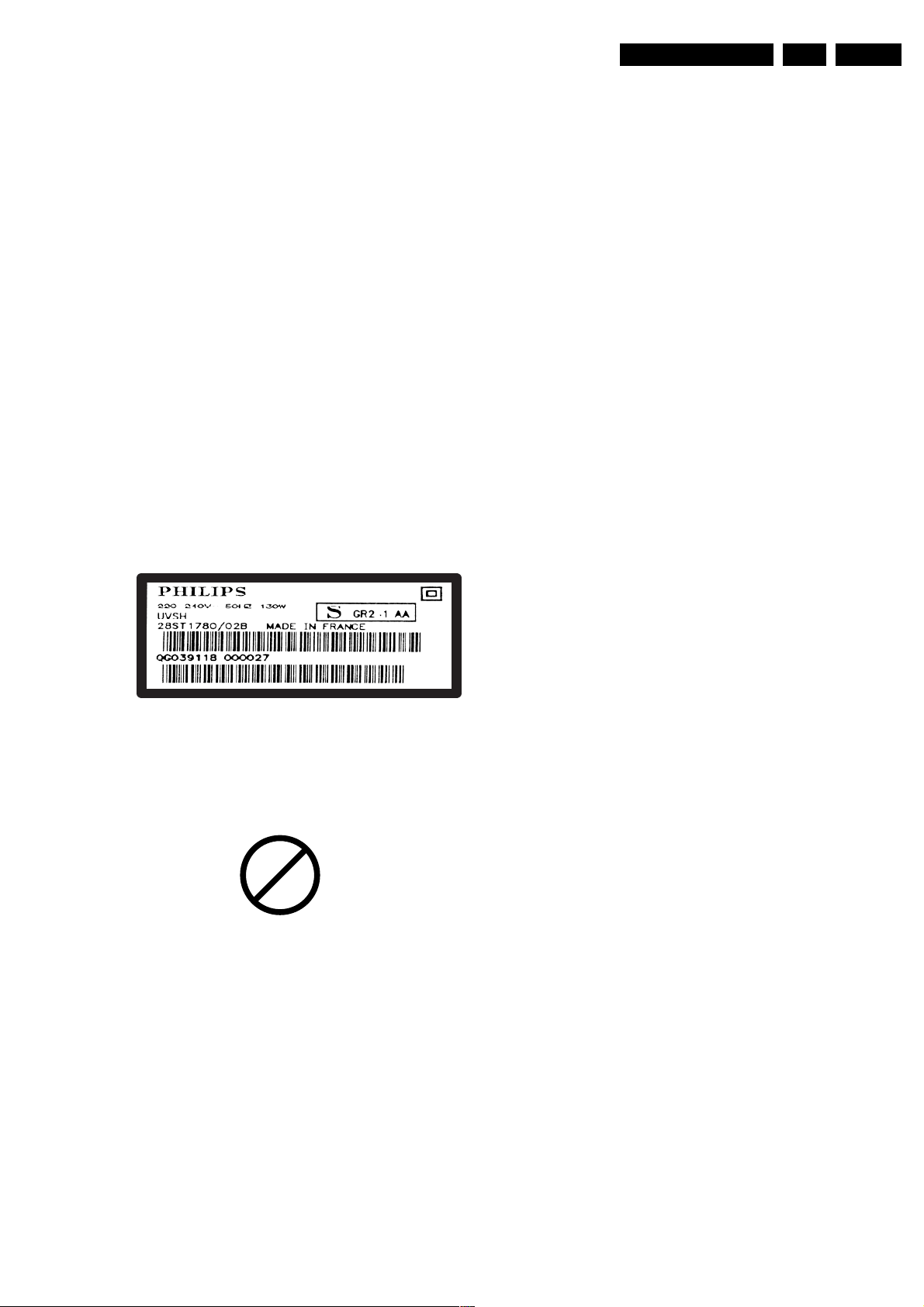
Identification: The bottom line of a type plate gives a 14-digit
serial number. Digits 5 and 6 refer to the production year, digits
7 and 8 refer to production week (in example below it is 1991
week 18).
To avoid wear-out of tips, switch “off” unused equipment or
reduce heat.
• Mix of lead-free soldering tin/parts with leaded soldering
tin/parts is possible but PHILIPS recommends strongly to
avoid mixed regimes. If this cannot be avoided, carefully
clear the solder-joint from old tin and re-solder with new tin.
• Use only original spare-parts listed in the Service-Manuals.
Not listed standard material (commodities) has to be
purchased at external companies.
• Special information for lead-free BGA ICs: these ICs will be
delivered in so-called "dry-packaging" to protect the IC
against moisture. This packaging may only be opened
shortly before it is used (soldered). Otherwise the body of
the IC gets "wet" inside and during the heating time the
structure of the IC will be destroyed due to high (steam-)
pressure inside the body. If the packaging was opened
before usage, the IC has to be heated up for some hours
(around 90°C) for drying (think of ESD-protection!).
Do not re-use BGAs at all!
• For sets produced before 1.1.2005, containing leaded
soldering tin and components, all needed spare parts will
be available till the end of the service period. For the repair
of such sets nothing changes.
In case of doubt whether the board is lead-free or not (or with
mixed technologies), you can use the following method:
• Always use the highest temperature to solder, when using
SAC305 (see also instructions below).
• De-solder thoroughly (clean solder joints to avoid the
mixing of two alloys).
E_06532_024.eps
230205
Figure 2-1 Serial number example
Regardless of the special lead-free logo (which is not always
indicated), one must treat all sets from this date onwards
according to the rules as described below.
P
b
Figure 2-2 Lead-free logo
Due to lead-free technology some rules have to be respected
by the workshop during a repair:
• Use only lead-free soldering tin Philips SAC305 with order
code 0622 149 00106. If lead-free solder paste is required,
please contact the manufacturer of your soldering
equipment. In general, use of solder paste within
workshops should be avoided because paste is not easy to
store and to handle.
• Use only adequate solder tools applicable for lead-free
soldering tin. The solder tool must be able:
– To reach a solder-tip temperature of at least 400°C.
– To stabilise the adjusted temperature at the solder-tip.
– To exchange solder-tips for different applications.
• Adjust your solder tool so that a temperature of around
360°C - 380°C is reached and stabilised at the solder joint.
Heating time of the solder-joint should not exceed ~ 4 sec.
Avoid temperatures above 400°C, otherwise wear-out of
tips will increase drastically and flux-fluid will be destroyed.
Caution: For BGA-ICs, you must use the correct temperature
profile, which is coupled to the 12NC. For an overview of these
profiles, visit the website www.atyourservice.ce.philips.com
(needs subscription, but is not available for all regions).
You will find this and more technical information within the
"Magazine", chapter "Workshop information".
For additional questions please contact your local repair help
desk.
2.3.5 Practical Service Precautions
• It makes sense to avoid exposure to electrical shock.
While some sources are expected to have a possible
dangerous impact, others of quite high potential are of
limited current and are sometimes held in less regard.
• Always respect voltages. While some may not be
dangerous in themselves, they can cause unexpected
reactions that are best avoided. Before reaching into a
powered TV set, it is best to test the high voltage insulation.
It is easy to do, and is a good service precaution.
Page 6

EN 6 TE3.1E CA3.
3. Directions for Use
You can download this information from the following websites:
http://www.philips.com/support
http://www.p4c.philips.com
Directions for Use
Page 7

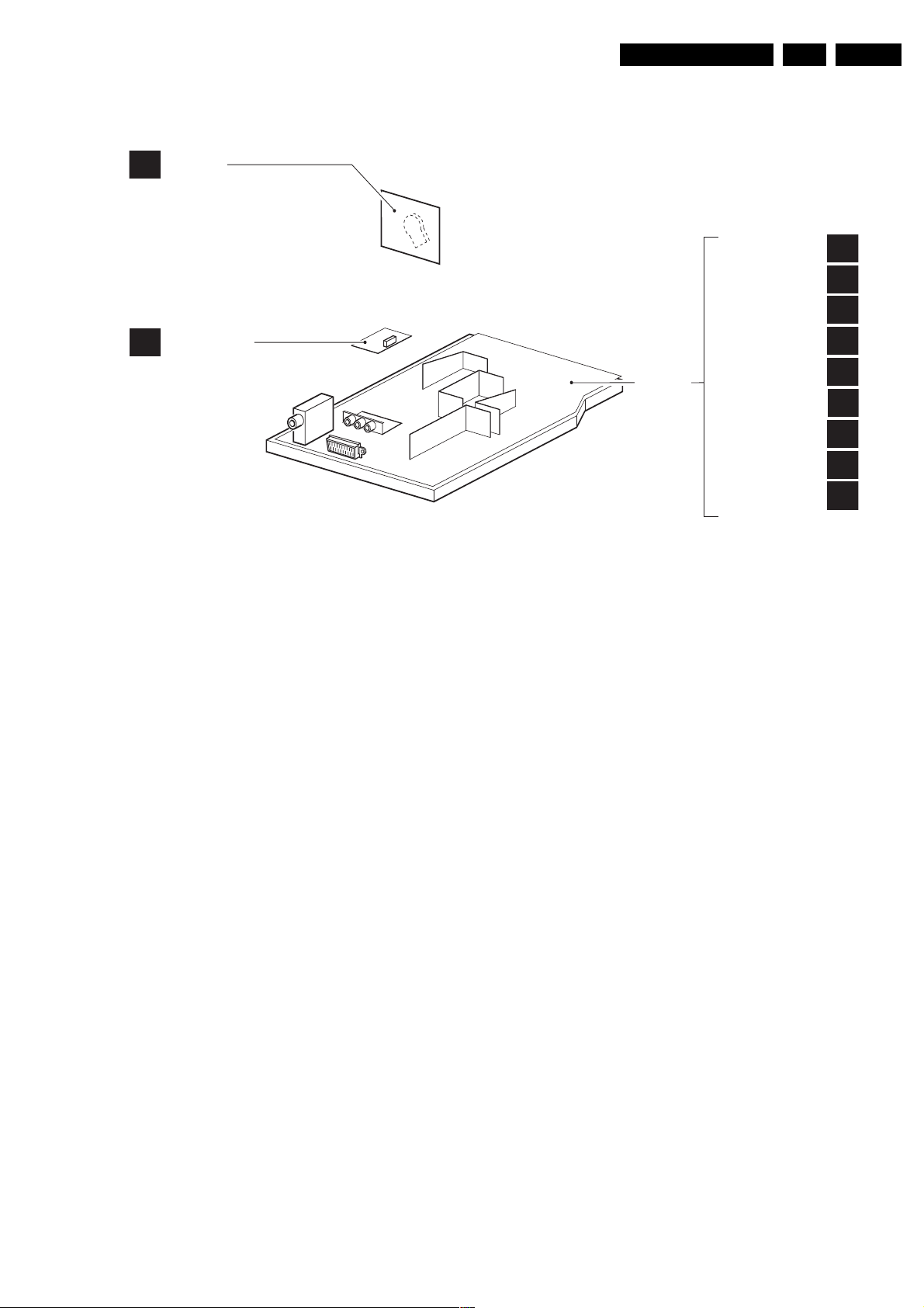
4. Mechanical Instructions
Index of this chapter:
4.1 Exploded view
4.2 Rear Cover Removal
4.3 Service Position Main Panel
4.4 Side I/O Panel Removal
4.5 Rear Cover Mounting
4.1 Exploded View
Mechanical Instructions
EN 7TE3.1E CA 4.
4.2 Rear Cover Removal
1. Remove all fixation screws (9x) of the rear cover.
2. Pull the rear cover a little backwards.
3. Now pull the rear cover backwards to remove it.
4.3 Service Position Main Panel
1. Remove the main panel [1]. At the same time, pull the
panel away from the CRT [2].
2. Turn the panel 90 degrees clockwise [3].
3. Flip the panel 90 degrees [4], with the components towards
the CRT
4.4 Side I/O Panel Removal
Remove the side I/O panel after unscrewing the screws (2x) at
the bottom of the set.
4.5 Rear Cover Mounting
Figure 4-1 Exploded view
F_15850_028.eps
20050824
To reassemble the set, perform all described processes in
reverse order.
Be sure that, before the rear cover is mounted:
• The mains cord is mounted correctly in its guiding bracket.
• All wires/cables are returned in their original position
Page 8
EN 8 TE3.1E CA5.
Service Modes, Error Codes and Fault Finding
5. Service Modes, Error Codes and Fault Finding
Index of this chapter
1. Service Modes
2. Fault Finding
5.1 Service Modes
The Service Mode offers features, which the service technician
can use to repair a set. Any feature change, made via the
Service Menu, will respond at the same time. All displayed text
strings in the Service Modes are in English.
5.1.1 TV Service Mode
Purpose
• To perform alignments (e.g. colour adjustment and
geometry alignments)
• To change option settings
Specifications
All service unfriendly modes (if present) are disabled, like:
• Auto switch 'off' (when there is no 'ident' signal)
• Timer switch to a channel
• Automatic user menu time-out
• The NVM is unprotected
• AV functions are not working
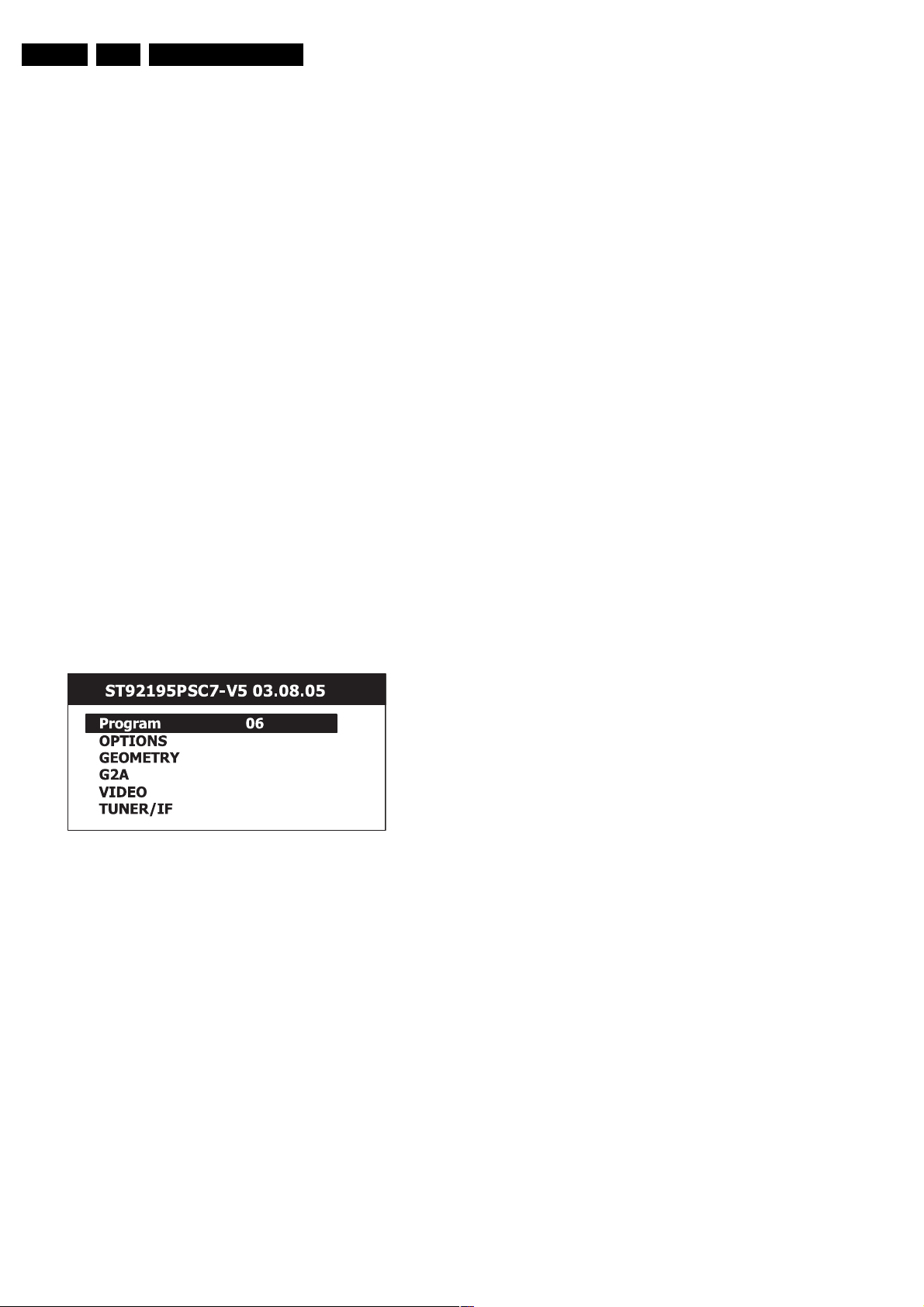
How to enter the Service Mode
Screen menu's must be 'off', when you enter the Service Mode.
Use a standard customer RC transmitter and key in the code
062596 directly followed by the MENU button in 10 seconds.
The following screen is visible when you enter the Service
Mode:
How to navigate
• Select menu items with the CURSOR UP/DOWN keys.
• With the CURSOR LEFT/RIGHT keys, it is possible to
change the value of the first item (Program)
• With the CURSOR RIGHT and OK keys, activate the
selected menu item.
• When you press the MENU key in a sub menu, you will
return to the previous menu.
• When you press the MENU key in the Service Mode menu,
you will return to the Main menu.
How to exit
• With the STANDBY command, the set switches to
Standby.
• With the MENU key, the set returns to the Main menu.
Switching the set 'off' and 'on' with the mains switch, brings
the set into normal operation again. All changes in the
Service Mode are stored immediately.
F_15850_005.eps
160805
Figure 5-1 TV Service Mode Menu
• LLLLLLL. This is the used IC type.
• PAB#-XX. This is the software identification.
– P = Philips.
– A = the region (W = West Europe, E = East Europe).
– B = sound specification (M = Mono, S = Stereo).
– # = number of TXT pages.
– XX = the software version number (the first X is the
main software version number and the second X is the
sub software version number).
• PROGRAM. .......
• OPTIONS. Three codes possible.
• GEOMETRY. To align the geometry (see chapter 8.x for a
detailed description).
• G2A. To align the G2 (see chapter 8.x for a detailed
description).
• VIDEO. To adjust RGB, R_cut-off and G_cut-off.
• TUNER/IF. To align the tuner.
Page 9
Service Modes, Error Codes and Fault Finding
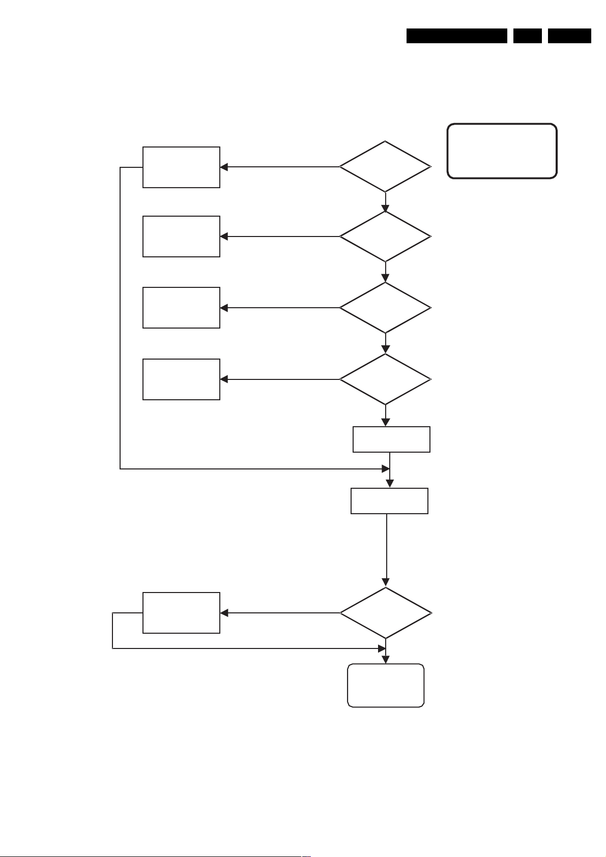
5.2 Fault Finding
5.2.1 Fault Tracing Diagram for Power Supply
D101-04
C101-04
C106, T101
YES
Fuse
F1
Defective
NO
EN 9TE3.1E CA 5.
Switched mode
Power Supply defective,
+123V is missing or
level is wrong
R107, R105
open
circuit
R104
R111, D107
D116,
NO
YES
YES
Voltage at
drain of
T101
YES
Voltage at
I101 pin 3
< 1V
NO
start-up
voltage pin
8
< 8V
NO
I101
NO
Measure
V102, R159
NO
Figure 5-2 Fault Tracing
adjustable with
Control range of
switched-mode
Power Supply
+123V
V101
YES
F_15850_006.eps
160805
Page 10

EN 10 TE3.1E CA5.
Service Modes, Error Codes and Fault Finding
Page 11
Block Diagrams, Test Point Overviews, and Waveforms
6. Block Diagrams, Test Point Overviews, and Waveforms
Wiring Diagram
11TE3.1E CA 6.
U_MCU
MCU.Sch
AV_STATUS
AV1/ AV2
A2-A7
SCL
SDA
U_S OUND
SOUND.Sch
AV2_
AUDL
AV2_ AUDR
LDVD/SC2L
RDVD/ SC2 R
SCL
SDA
L1 OUT
R1OUT
L1IN
R1I N
L2IN
R2I N
L2
OUT
R2OUT
A3
STDBY
DVD_SB
DVD_ S TB
BRST_ON/
FF
V
_OSD
HOSD
L/L A
CVBS_ TXT
B_ OSD
G_OSD
R_ OSD
U_PO WE R
POWER.Sch
STDBY
DVD_SB
O
DVD_ S TB
BRST_ ON/OFF
A9
U_C RT
CRT.S ch
A13
U_M ISP ART
MISPART.Sch
U_SCART
SCART.Sch
U_TUNER
TUNER.S ch
A1
A10
CVBS_TXT
R
G
DVD/SC2-SEL
CVBSOUT
FBEXT
CVBSEXT
BRST_ ON/OFF
SCL
SDA
AGC
IF1
IF2
A8
U_V IDEO
VIDEO.Sch
R
B
G
B
CVBSOUT
FBEXT
CVBSEXT
A5
U_D EFLE CTIO N
DEFLECTION.S ch
V_ O S D
A4-A12
SCL
SDA
AGC
IF1
IF2
BCLG
V_AMP
HOSD
HOUT
VE R T
BCLG
V_AMP
HOSD
HOUT
VE R T
F_15850_013.eps
220805
Page 12

Block Diagrams, Test Point Overviews, and Waveforms
Block Diagram Main
12TE3.1E CA 6.
F_15850_011.eps
220805
Page 13

Block Diagrams, Test Point Overviews, and Waveforms
Block Diagram Power Supply
13TE3.1E CA 6.
F_15850_014.eps
220805
Page 14

Block Diagrams, Test Point Overviews, and Waveforms
I2C Diagram
14TE3.1E CA 6.
A1
RENUT
4
5
R614
R613
SDA
SCL
A5
R333
R334
51 52
VIDEO
PROC.
SDA
SCL
A2
R048 R049
65
EEPROM
SDA
SCL
A6
R013 R012
+5V
20 19
MCU
A3
SDA
SCL
R208R207
78
MSP
F_15850_012.eps
220805
Page 15

Circuit Diagrams and PWB Layouts
7. Circuit Diagrams and PWB Layouts
Main Panel: Tuner
15TE3.1E CA 7.
4321
A1 A1
D
C
B
A
TUNER
GND-PWR
GND-PWR
CT17
47U50
C076
10N
D027
LL4148
N307
CGA
1
N308
N608
R755
10K
GND-PWR
GND-PWR
RT22
CHR0805-1R00
LT05
IND500-1U0H
MONO-IN
N233
2
RT34
0R
TT01
UV1316
NUT
R701
10K
C079
47N
SCL
SDA
II - TUNER
0
GND
3FHV41FHV
FHU
3
N715
5V56
N716
V5
6
N599
TFA
7CN8CN9
CT03
0R 1/10W
2FI
01
N718
LT02
150R 1/4W
GND-PWR
GND-PWR
CT07
100U50
RT07
N773
100R
RT09
N766 N767
100R
CT27
CT26
47P
47P
GND-PWRGND-PWR
SCL
SDA
J027
RT29
10K
RT28
10K
+5V
N012
Q030
BC547B
N638
RT38
390R
N634
RT35
0R
RT33
0R
GND-PWR
1FI
11
N717
N719
CT13
GND-PWR
RT17
22K
CT01
100N
N625
J207
GND-PWR
N626
CT02
100N
10P
5V 5V
RT12
N042
6K8
RT13
LT04
IND500-1U0H
CT08
1N
N294
GND-PWR
RT06
1K
RT40
22K
DT02
BA582
N620
DT03
BA582
FT02 K3953M
RT15
5
N337
0R
RT16
4
0R
N298
CT11
10N
N630
RT23
5K6
GND-PWR
GND-PWRGND-PWRGND-PWR
N297
CT12
10N
CT09
1N
N295
MONO-IN
2
1
3
GND-PWR
CT20
390P
GND-PWR
CT25
100N
RT08
100R
RT10
100R
AUDIO_TUNER2
+5V
CT28
22P
CT33
470N
J026
N087
AUDIO_TUNER2
CT34
220N
SDA
SCL
GND-PWR
II - TUNER AUDIO AMPLIFIER
LT01
10uH
IND500-10UH
N079
J107
33V
RT20
680K
N720
GND-PWR
6K8
TT02
BC847
N324
FT01 K9453M
1
N325
2
3
GND-PWR
IT01
1
N624
N293
CT04
100N
GND-PWR
CT22
470N
N296
CT10
1N
N621
GND-PWR
N622
CT29
22P
GND-PWRGND-PWR
RT02
10K
GND-PWR GND-PWR
N301
N618
RT39
10K
IF1
2
IF2
3
OP1
4
FMPLL
5
DEEM
6
AFD
7
DGND
8
AUD
9
TOP
10
10
SDA
SDA
11
SCL
12
SIOMAD
DELEAT
TDA9886
RT11
123
N623
100R
GND-PWR
RT21
220K
5
4
SIF2
SIF1
AFC
VP
VPLL
AGND
CVBS
VAGC
REF
TAGC
NC
FT03
TPW02B
DT01
BA582
N334
N419
N417
24
23
22
21
20
19
N420
18
17
16
15
14
13
N335N336
N629
CT21
220N
GND-PWR
RT18
100R
N418
XT01
4MHZ HC49
N338
GND-PWR
RT26
12K
GND-PWR
CT23
470N
N726
N454
5VM
CT06
100N
SCL
SDA
CT15
10P
J071J070
CT24
1N5
N051
R613
100R
GND-PWR
R614
100R
GND-PWR
J067
RT05
22K
N299N300
GND-PWR
GND-PWR
RT01
100K
GND-PWR
RT03
0R
+5V
GND-PWR
N452N453
C607
100P
C608
100P
J073
N013
LT03
10uH
N725
GND-PWR
RT14
330R
RT25
12K
CGA
NUT
1
2
GND-PWR
R602
27K
GND-PWR
5V
X101
UV1316
RT04
0R
N597
33V
CT05
100N
N628
MAIN TUNER
3FHV41FHV
FHU
3
N619
GND-PWR
GND-PWR
N627
J239
CT14
10P
N421
5V56
C601
47U25
CT16
10U25
RT24
620R
N598
GND-PWR
N182
V5
7CN8CN9
6
GND-PWR
C606
100N
LT07
4.7uH
N631
123
GND-PWR
TFA
N078
C603
100N
GND-PWR
RT36
100R
N635
GND-PWR
C627
10N
GND-PWR
FT04
TPW02B
01
2FI
N636
RT30
1K
GND
11
C602
100U16
RT32
10K
0
GND-PWR
1FI
N198
L602
1uH
N199
5VM
N050
J995 J257
N632
RT27
10R
Q027
GND-PWR GND-PWR
BC848BLT1
RT37
220R
N637
GND-PWR
N128
C605
8P2
L601
10uH
R601
4K7
R606
15K
D601
LL4148
FOR SECAM L
ELSE D601 JUMPER
CT31
100N
GND-PWR
N633
CT30
100N
RT31
75R
J080
CVBS_TUNER2
GND-PWR
IF1
IF2
AGC
LT06
10uH
IND500-10UH
CT32
10U25
CVBS_TUNER2
C260
10N100V
IF1
IF2
AGC
+5V
N260
A
5V
GND-PWRGND-PWRGND-PWR
1 2 3 4
K100
F_15850_015.eps
220805
D
C
B
A
Page 16

Circuit Diagrams and PWB Layouts
Main Panel: EEPROM and MCU
16TE3.1E CA 7.
4321
D
C
B
A
A2
A6
EEPROM
VSTB
VCLK
VDATAOUT
VDATAIN
MCU
S002
1
2
3
4
5
6
DVD TV
+5V
GND-PWR
6V5
C006
47U25
C001
10U50
N467
R001
220R
GND-PWR
DVD/SC2-SEL
AV_STATUS
L/LA
AV1/AV2
STDBY
B_OSD
G_OSD
R_OSD
SDA
SCL
R120 1K
1 2 3 4
N640
GND-PWR
N005
D003
2.7V ZENER
J241
N507
GND-PWR
DVD OPT.
J098
N807
N201
R179
0R
R063 0R
R062 0R
C026
22P
C028
22P
C027
22P
C002
22P
VDATAIN
N789
IR_DVD
N302
VSTB
VCLK
VDATAOUT
J100
IR_DVD
GND-PWR
J147
J149
N796
C032
22P
GND-PWR
C033
4N7
RW OPT.
R178
18K
N795
J148
N202
R011
R055
220R
R064
220R
100R
T003
BC858BLT1
N663 N664
R056
4K7
GND-PWR GND-PWR
DVD/SC2-SEL
AV_STATUS
R043
4K7
GND-PWR
J998
N094
N093
J112
N010
R013
4K7
+5V+5V
R012
4K7
R015
4K7
R007
4K7
+5V+5V+5V
R010
4K7
L/LA
J134 J173
AV1/AV2
J019 J029J058
N779
STDBY
B_OSD
G_OSD
R_OSD
N737
N778
J009
N101 N102
J008
J007
N736
N777
SDA
N768
SCL
J078 J087 J106
5VA
C003
10U50
GND-PWR
GND-PWR
RTC
D050
N506
LL4148
D052
1N5226B 3.3 V ZENER
R124
2K2
N508
C045
470U16
SUPERCAP 0.1F
D051
LL4148
Y002
R123
10K
32.768KHZ HC49S
C043
100N
C123
N728
N727
N242
GND-PWRGND-PWRGND-PWR
R035
4K7
N239
S_SEL_1
S_SEL_2
S_SEL_3
FB_OSD
5VD
C008
100N
22P
1
2
3
4
+5VDVDRW
R033
4K7
GND-PWR
GND-PWR
U004
XTAL1
XTAL2
RST
VSS
PCF8593
R034
10K
C004
100U16
N237
C010
2N2
S_SEL_1
S_SEL_2
S_SEL_3
N754
N168
FB_OSD
N163
C005
100N
GND-PWR
R022
5K6
VDD
INT
SCL
SDA
N203
N240
N144N147
N751
J092 J093
N216
N095
R016
R017
R018
R019
N049
GND-PWR
C009
22P
N309
8
7
6
5
J090
N047
N723
N722
R009
220R
J094
N477
D006
LL4148
N236
10
10
10
N753
11
11
11
N755
12
12
12
13
13
13
14
14
14
15
1K
15
15
N471
16
1K
16
16
N472
17
1K
17
17
N473
18
18
18
470R
N474
19
19
19
20
20
20
21
21
21
22
22
22
23
23
23
24
24
24
25
25
25
26
26
26
27
27
27
28
28
28
R121 100R
R122 100R
I001
1
1
1
2
2
2
3
3
3
4
4
4
5
5
5
6
6
6
7
7
7
8
8
8
9
9
9
ST92195
GND-PWR
C034
56P
N204 N205 N206
+5VDVDRW
R008
4K7
R061
0R
N490
56
56
P20
P20
P20
RESET
RESET
RESET
P07
P07
P07
P06
P06
P06
P05
P05
P05
P04
P04
P04
P03
P03
P03
P02
P02
P02
P01
P01
P01
P00
P00
P00
P37
P37
P37
P36
P36
P36
P35
P35
P35
P34
P34
P34
BLUE
BLUE
BLUE
GREEN
GREEN
GREEN
RED
RED
RED
FB
FB
FB
SDA
SDA
SDA
SCL
SCL
SCL
VCC
VCC
VCC
JTDO
JTDO
JTDO
WSCF
WSCF
WSCF
WSCR
WSCR
WSCR
AVDD3
AVDD3
AVDD3
TEST
TEST
TEST
MCFM
MCFM
MCFM
JTCK
JTCK
JTCK
C042
100N
OSCOUT
OSCOUT
OSCOUT
P21
P21
P21
P22
P22
P22
P23
P23
P23
P24
P24
P24
P25
P25
P25
OSCIN
OSCIN
OSCIN
P47
P47
P47
P46
P46
P46
P45
P45
P45
P44
P44
P44
P43
P43
P43
P42
P42
P42
P41
P41
P41
P40
P40
P40
VSYNC
VSYNC
VSYNC
HSYNC
HSYNC
HSYNC
AVCC
AVCC
AVCC
PLLR
PLLR
PLLR
PLLF
PLLF
PLLF
VSS
VSS
VSS
AGND
AGND
AGND
CVBS1
CVBS1
CVBS1
CVBS2
CVBS2
CVBS2
JTMS
JTMS
JTMS
AVDD2
AVDD2
AVDD2
CVBS0
CVBS0
CVBS0
TXCF
TXCF
TXCF
56
55
55
55
54
54
54
N354
53
53
53
N119
52
52
52
N353
51
51
51
N352
50
50
50
N351
49
49
49
48
48
48
47
47
47
N110
46
46
46
45
45
45
44
44
44
43
43
43
42
42
42
41
41
41
40
40
40
39
39
39
38
38
38
37
37
37
36
36
36
35
35
35
34
34
34
33
33
33
32
32
32
31
31
31
30
30
30
29
29
29
N478
GND-PWR
C029
22P
J102 J103
N348
BRST_ON/OFF
J627
N347
N346
N345
N344
N342
N341
N340
N339
R023
15K
C013
2N2
SCL
SDA
N117N118
C022
22P
C030
22P
GND-PWR
+5V
R057
10K
R002
2K2
GND-PWR
X001
4MHZ
N109
R025
5K6
C014
470N
N355
J125
R030
10K
J626
DVD_STB
N479
C019
4N7
GND-PWR
C016
470N
C015
100P
5VA
+5V
N207
N662
T002
BC848BLT1
N356
J127
+5V
R065
10K
N116
J066
+5V
C023
22P
GND-PWR
BRST_ON/OFF
DVD_STB
N137N138
J129 J130 J131
C020
100N
GND-PWR
N488
J116J117J118J121
N046
IR01
34836
GND-PWR
CHR-SW
N115
J126
N136
GND-PWR
5VA
BC848BLT1
N238
R047
4K7
N349
T001
N003
J122
R059
220R
R040
1K5
JS01
0R
+5V
C031
100P
D013
STDBY
N350
J124
R054
4K7
CCV
CHR-SW
R072
10K
N343
GND-PWR
DNG
RI
GND-PWR
N208
N494
+5V
D004
LL4148
TXT-SW
C041
GND-PWR
D001
LL4148
N194
R058
47K
SDA
SCL
GND-PWR
GND-PWR
IR_TV
KEYB
GND-PWR
+5V
+5V
R024
10K
GND-PWR
+5V
D005
LL4148
R080 10K
R081 10K
N139
R060
10U
4K7
R044
10K
N006
470P
GND-PWR GND-PWR
N661
R053
47K
GND-PWR
3
2
1
JC01
EXT INFRARED
3
2
N764
1
1
+5V
2
3
4
N489
5
N211
6
J164
N639
4
3
2
1
REC_LED&EJECT
N665
T005
BC848BLT1
N055
R032
4K7
DVD_SB
D002
+5V
LL4148
N784
SDA
SCL
N769
J291
S004
COMPAIR
S001
IR&LED
S003
N175
GND-PWR
C080
10N
SC01
1
2
3
4
5
SERVICE
J074J082 J175J176
J182J183J184J185J186J274J275
J181
N040N043
N070
12(3V3)V
5VS
R052
N487
10K
+5V
DVD_SB
C025
1U50
GND-PWR
+5V
R045
N292
CD28
470N16VC024
10K
J011
N130N131
R027
4K7
N179
C040
470N
R049
N424
100RR048
100R
5
SDA
6
SCL
7
N484
PTC
8
VDD
IC02 24 C16
N485
+5V
KEYB
SCL
SDA
5VM
GND-PWR
R003
220R
N486
R028
0R
J075
HOSD
CVBS_TXT
TXT-SW
C011
100N
J114J115
N770
N468
R051
470R
SW01 SW02
CH+ CH-
GND-PWR
R077
5K6
N033 N034
N035
VOL
V_OSD
N786
USS
A2
A1
A0
A2 A6
N209N210
J119
R004
R005
820R
560R
N469 N470
N177
GND-PWR
R076
1K5
N495 N496
5V
N037
N032
J177
N030N031
VOL
V_OSD
HOSD
CVBS_TXT
4
3
2
1
GND-PWR
N660
GND-PWR
R006
1K5
SW04
VOL+
D030
N497
BAT85
SW03
VOL-
GND-PWR
J300J301
F_15850_016.eps
220805
D
C
B
A
Page 17

Main Panel: Sound
Circuit Diagrams and PWB Layouts
17TE3.1E CA 7.
4321
A3 A3
SOUND
GND-PWR
D
C207
100N
5V
GND-PWR
N036
R209
47K
N097N098
J135
C216
R207
R208
C208
10U50
C075
22U50
100R
100R
C215
470N
GND-PWR
C209
100N
GND-PWR
C210
100N
C077
22U50
N527
N528
GND-PWR
N248 N249 N250
GND-PWR
N255
N256
SCL
SCL
SDA
SDA
N774
N775 N776
J085 J105 J108
5V
C
AV2_AUDR
AV2_AUDL
AV2_AUDR
AV2_AUDL
J160 J136
N096
TV_S/R
TV_S/L
470N
GND-PWR
C218
1N
GND-PWR
C217
1N
SOUND PROCESSOR
I202 MSP 3415G
1
1
N529
N247
J153J139
1
2
2
2
3
3
3
4
4
4
5
5
5
6
6
6
7
7
7
8
8
8
9
9
9
10
10
10
11
11
11
12
12
12
13
13
13
14
14
14
15
15
15
16
16
16
17
17
17
18
18
18
19
19
19
20
20
20
21
21
21
22
22
22
23
23
23
24
24
24
25
25
25
26
26
26
NC
NC
NC
AUD_OL_OUT
AUD_OL_OUT
AUD_OL_OUT
D_CTH_OUT_1
D_CTH_OUT_1
D_CTH_OUT_1
D_CTR_OUT_0
D_CTR_OUT_0
D_CTR_OUT_0
ADR_SEL
ADR_SEL
ADR_SEL
STANDBYQ
STANDBYQ
STANDBYQ
I2C_CL
I2C_CL
I2C_CL
I2C_DA
I2C_DA
I2C_DA
I2S_CL
I2S_CL
I2S_CL
I2S_WS
I2S_WS
I2S_WS
I2S_DA_OUT
I2S_DA_OUT
I2S_DA_OUT
I2S_DA_IN1
I2S_DA_IN1
I2S_DA_IN1
ADR_DA
ADR_DA
ADR_DA
ADR_WS
ADR_WS
ADR_WS
ADR_CL
ADR_CL
ADR_CL
DVSUP
DVSUP
DVSUP
DVSS
DVSS
DVSS
I2S_DA_IN2
I2S_DA_IN2
I2S_DA_IN2
NC
NC
NC
RESETQ
RESETQ
RESETQ
DACA_R
DACA_R
DACA_R
DACA_L
DACA_L
DACA_L
VREF2
VREF2
VREF2
DACM_R
DACM_R
DACM_R
DACM_L
DACM_L
DACM_L
DACM_SUB
DACM_SUB
DACM_SUB
XTAL_OUT
XTAL_OUT
XTAL_OUT
ANA_IN2+
ANA_IN2+
ANA_IN2+
ANA_IN1+
ANA_IN1+
ANA_IN1+
SC1_OUT_L
SC1_OUT_L
SC1_OUT_L
SC1_OUT_R
SC1_OUT_R
SC1_OUT_R
SC2_OUT_L
SC2_OUT_L
SC2_OUT_L
SC2_OUT_R
SC2_OUT_R
SC2_OUT_R
XTAL_IN
XTAL_IN
XTAL_IN
TESTEN
TESTEN
TESTEN
ANA_IN-
ANA_IN-
ANA_IN-
AVSUP
AVSUP
AVSUP
AVSS
AVSS
AVSS
MONO_IN
MONO_IN
MONO_IN
VREFTOP
VREFTOP
VREFTOP
SC1_IN_R
SC1_IN_R
SC1_IN_R
SC1_IN_L
SC1_IN_L
SC1_IN_L
SC2_IN_R
SC2_IN_R
SC2_IN_R
SC2_IN_L
SC2_IN_L
SC2_IN_L
SC3_IN_R
SC3_IN_R
SC3_IN_R
SC3_IN_L
SC3_IN_L
SC3_IN_L
AGNDC
AGNDC
AGNDC
AHVSS
AHVSS
AHVSS
CAPL_M
CAPL_M
CAPL_M
AHVSUP
AHVSUP
AHVSUP
CAPL_A
CAPL_A
CAPL_A
VREF1
VREF1
VREF1
N394
X201
52
52
52
18.432MHZ
51
51
51
N393
50
50
50
GND-PWR
49
49
49
48
48
48
47
47
47
46
46
46
45
45
45
44
44
44
43
43
43
42
42
42
41
41
41
40
40
40
39
39
39
38
38
38
37
37
37
36
36
36
35
35
35
34
34
34
33
33
33
32
32
32
31
31
31
30
30
30
29
29
29
28
28
28
N373
27
27
27
N371
C242
N392
N391
N390
N389
N183
GND-PWR
N387 N388
N386
N385
N384
N383
N382
N381
N380
N379
GND-PWR
N377
N376
N375
N374
GND-PWR
J234
N370
J233
56P
C240
56P
C221
22U50
C219
22U50
C236
3.3U50
C235
100N
C227
100N
N372
C241
56P
N378
C222
22U50
C220
22U50
N746
C245
2P2
C244
2P2
GND-PWR
GND-PWR
N257
GND-PWR
GND-PWR
GND-PWR
N742
N226
GND-PWR
GND-PWR
J111
C228
3.3U50
C226
10U50
C223
10U50
L2OUT
R2OUT
C257
330N
C233
330N
C231
330N
C229
330N
N222
F201
TPSRD 4.43
GND-PWR
N086
N232
L2OUT
R2OUT
R211
C239
10U50
N220
GND-PWR
R212
75R
0R
C234
330N
C232
330N
C230
330N
R210
0R
GND-PWR
C238
100N
N740
N743
C224
10U50
R224
100R
N038
AM_MONO
R1IN
L1IN
R2IN
L2IN
RDVD/SC2R
LDVD/SC2L
C225
100N
L1OUT
R1OUT
N759N760N761
5V
SC
J077J109 J110
GND-PWR
AM_MONO
R1IN
L1IN
R2IN
L2IN
RDVD/SC2R
LDVD/SC2L
8V
GND-PWR
L1OUT
R1OUT
SC
N756
D
C
AUDIO AMPLIFIER
R201
JMP
C201
1000U25
GND-PWR
N802
D507
LL4148
I201
TDA7057Q
1NC.V
1NIV
3
1CN2
N524
C259
100N
N364 N365 N366 N367
GND-PWR
C206
10U50
GND-PWR
C202
4.7U50
N525 N526
R204
R203
1K
4K7
N782
L/S_VT
GND-PWR
GND-PWR GND-PWR
PUSV
DNGS
2NIV
5
6
4
GND-PWR GND-PWR GND-PWR
GND-PWR
C203
4.7U50
R205
C204
1K
10N
GND-PWR
B
+12VA
VOL
J293 J294 J295
N073
T151
BC847B
N538
R226
2k
N679
C258
100uf
N539
R228
A
6V5
R229
100k
22k
N019 N020N021
J200 J201 J202 J028
VOL
16V
N072
N074
T150
R227
BC847B
1K2
N537
J083 J084
R225
2k
N678
N022
N803 N804
D508
1N4148
GND-PWRGND-PWR GND-PWR
1 2 3 4
2DNGP
+2TUO
2NC.V
8
7
9
R206
4K7
C205
10N
N783
R/S_VT
R202
4K7
-2TUO01-1TUO
1DNGP
+1TUO
11
21
31
N369
S202
5
GND-PWR
4
3
2
1
H.P.
N368
B
A
F_15850_017.eps
220805
Page 18

Main Panel: Deflection
Circuit Diagrams and PWB Layouts
18TE3.1E CA 7.
4321
A4
A10
D
C
VERTICAL DEFLECTION
HORIZONTAL DEFL.
D406
BYV36C
N568
R413
5K6 3W
C515
220N400V
!
R403
100R
N563
C402
10N
N695
GND-PWRGND-PWRGND-PWRGND-PWR
VERTICAL DEFLECTION
HOUT
16V
HOUT
N285
C414
1U250
GND-PWR GND-PWR
R401
4R7
C401
100U25
N562
GND-PWR
T401
BC639
N284
N196
C407
100N
D402
LL4148
R402
47K
!
C413
1N2KV
1
L401
2
3
602300033071
C405
100N
L403
100uH
N569
N443
125VOUT
R414
1K
5
0.22R 1/2W
4
R160
125V
D401
BYV36C
R404
N445
L402
200uH
R405
39R
N564
5R6 5W
S403
N444
2
1
HDY
!
T402
BU508DF
GND-PWR
GND-PWR
I401 TDA1771
S401
CRT BRD
C403
OPT.
GND-PWR GND-PWR
C419
1U160V
GND-PWR
N650
R407
470K
N651
321
4
GND-PWR
RETAEH
ADNG
V571+
C404
6N8 2KV
C408
22U160
GND-PWR
C409
10U250
GND-PWRGND-PWR
N696
D405
BYV36C
HORIZONTAL DEFLECTION
L404 604200000391
ABL
HOSD
14
EHT
13
FOCUS
12
11
8
10
4
3
76
1
HORZ
125VOUT
+B
N081
R406
JUMPER
R409
JMP
N565
N566
N322
2
5
VID
9
H
GND
N189
E/W
24V
12V
GND
!
R332
560R
N191
J051
J054
J060
N193
G2
GND-PWRGND-PWR
HOSD
N447 N448
J218
J292
N446
R410
0.22R
N567
D407
BYV36C
GND-PWR GND-PWR
GND-PWR
C462
100P500V
N024
C411
100N
N571
R421
GND-PWR
1M
R429
2K
R415
2K
C417
100N
GND-PWR GND-PWR
C412
1000U35
R425
750K
N570
C418
100N
R422
1M
J205
A4
A10
D
R423
R424
1M5
1M5
N572N573
8V
N060
R412
2K4
R325
22K
R411
7K5
N105
J016
+24V_VERT
VC
BCLG
BCLG
C
NEGPMAR
DNG
5
6
R446
3K3
R449
91R
N582N583
C444
2200U25
TUO.FUB
7
N580
R445
8K2
NI.VNI
8SV9
01
NEG.BF
N287
N788
C445
100U50
B
VC
VC
+24V_VERT
D441
N579
1N4007
R448
2K0
R450
C443
N286
22U50
0.82R
GND-PWR
A
F_15850_018.eps
220805
THGIEH
NIGIRT
SVSO
TUO
4
2
1
3
N578
C442
47N
N787
GND-PWR
R428
N581
470R
R447
2K4
N574N575
J240
A
N585
R452 330R
R457
OPT.
N698
N697
GND-PWR
R456
180K
Q442
BC337-16
N466
Q443
BC327-16
N576
240J
J047J041
+24V_VERT
N025
R440
220R
R441
2R2
GND-PWR
R444 82KR455 4K7
C441
220N
N584
N577
B
VERT
S421
B
V_AMP
V_OSD
VERT
V_AMP
V_OSD
VERT
N785
J043
N799
J046
N801
A
GND-PWRGND-PWR GND-PWR
R454
47K
R451
6K8
R453
3K3
T441
BC848BLT1
R458
0R
1 2 3 4
Page 19

Main Panel: Video
Circuit Diagrams and PWB Layouts
19TE3.1E CA 7.
4321
D
C
B
A
A5
VIDEO
ICATH
N197
7.5V ZENER
AGC
SC
CVBSOUT1
T301
3
42
1HM
GND-PWR
DVD_Y/SC2_V
B
G
R
FBEXT
D311
N757
SC
J061 J069
N758
CVBSOUT1
LC1
1
LC2
44MH39PF
DVD_Y/SC2_V
B
G
R
FBEXT
LL 4148
0R OPTIONAL
AGC
CVBSEXT
CHR_DVD
R312
75R
D310
IF1
IF2
N320N321
R387
N560
10K
R388
C353
22N
47K
GND-PWR
IF1
1
IF2
2
N082
C348
10N
C350
R335
220P
100R
N544
J313
L302 8u2
123
GND-PWR GND-PWR
CVBSEXT
8V
J235
J065
CHR_DVD
R310
R311
75R
75R
D320
5V1 ZENER
J044
R361
680R
5V
F303
TB01B
R389
390K
BCLG
N104
T314
BC848BLT1
F301
K3953
GND-PWR
GND-PWR
C343
100P
N333
5V1 ZENER
(PAL I--J1981m)
3
C344
4N7
L301
10uH
N068
8V
R307
1K5
D321
BCLG
5
4
J006
L303
10uH
R308
1K5
J158
R303
120R
GND-PWR
D322
5V1 ZENER
GND-PWR
J311
GND-PWR
GND-PWR
C306
330N
GND-PWR
N437
J045
N278
C307
100U16
C308
100N
GND-PWRGND-PWR
N438
J247
C310
100U16
N540
GND-PWR GND-PWR
N140N142
N114
C314
1U50
GND-PWR
D323
5V1 ZENER
C301
1U16
C302
10U50
C303
22N
C304
1U50
C349
100N
GND-PWR
N132
C305
1N
N277
N261
N262
C309
100N
C312
1U50
C311
100N
C313
1U50
C315
1U50
C345
100N
C318
22N
C319
22N
C320
22N
C317
1U50
N265
J015
N269
R301
150R
J024
N266
N272
N274
N270
N331
N332
N328
N327
N550
N263N264
GND-PWR
N276
N279
LC1
LC2
N439
N267
J226
GND-PWR
N268
N561
N275
R309
330K
GND-PWR
5
4
N271
N227
N228
J246
N273
GND-PWR
1
1
1
2
2
2
3
3
3
4
4
4
5
5
5
6
6
6
7
7
7
8
8
8
9
9
9
10
10
10
11
11
11
12
12
12
13
13
13
14
14
14
15
15
15
16
16
16
17
17
17
18
18
18
19
19
19
20
20
20
21
21
21
22
22
22
23
23
23
24
24
24
25
25
25
26
26
26
27
27
27
28
28
28
N164
3
I301
NC/SIF1
NC/SIF1
NC/SIF1
NC/SIF2
NC/SIF2
NC/SIF2
NC/AGCSIF
NC/AGCSIF
NC/AGCSIF
VREF
VREF
VREF
AGCIF
AGCIF
AGCIF
PIFIN1
PIFIN1
PIFIN1
PIFIN2
PIFIN2
PIFIN2
AGCTU
AGCTU
AGCTU
IFPLL
IFPLL
IFPLL
GNDIF
GNDIF
GNDIF
FMOUT
FMOUT
FMOUT
VCCIF
VCCIF
VCCIF
CVBSOUT
CVBSOUT
CVBSOUT
EXTAUD
EXTAUD
EXTAUD
LC1
LC1
LC1
LC2
LC2
LC2
VCC2
VCC2
VCC2
CVBS1
CVBS1
CVBS1
GND
GND
GND
CVBS2
CVBS2
CVBS2
BS
BS
BS
CVBS3
CVBS3
CVBS3
CHR
CHR
CHR
APR
APR
APR
BEXT
BEXT
BEXT
GEXT
GEXT
GEXT
REXT
REXT
REXT
FBEXT
FBEXT
FBEXT
F302
K9453
1
2
STV2246H/48H
T302
R344
N545
68K
BC848BLT1
NTBC/CVBSOUT1
R341
10K
FMCAP
FMCAP
FMCAP
AUDOUT
AUDOUT
AUDOUT
GND
GND
GND
VCC
VCC
VCC
SDA
SDA
SDA
SCL
SCL
SCL
SLPF
SLPF
SLPF
LFB/SSC
LFB/SSC
LFB/SSC
HOUT
HOUT
HOUT
VERT
VERT
VERT
BCL
BCL
BCL
VCC1
VCC1
CVBSOUT1
CVBSOUT1
CVBSOUT1
GND1
GND1
GND1
VAMP
CLPF
XTAL1
XTAL2
XTAL3
FBOSD
ROSD
GOSD
BOSD
ICATH
ROUT
GOUT
BOUT
R342
10K
N330
GND-PWRGND-PWR
N084
N083
N329
56
56
56
55
55
55
54
54
54
GND-PWR
53
53
53
52
52
52
N415
51
51
51
N414
50
50
50
49
49
49
48
48
48
47
47
47
N797 N798N800
46
46
46
45
45
44
44
44
43
43
43
42
41
N408
40
N407
39
N406
38
N405
37
36
N404
35
N403
34
N402
33
N401
32
N400
31
N399
30
N398
29
N067
D307
BA282
D308
BA282
T303
BC848BLT1
N680
N214 N215 N217
R346
22K
J079J091
J022
AM_MONO
J209
N416
N085
J195
N772
J023
R334
100R
R333
100R
N765
N413
N412
N411
J039 J040
VERT
N410
N409
GND-PWR
C356
X302
N281
3.579MHZ HC49
0R
N160 N161N162
C323
100N
C321
100N
R343
10K
N319
GND-PWR
SDA
N771
SCL
VERT
GND-PWR
J018
C322
100N
R314
47K
8V
R345
2K2
L/LA
J168
AM_MONO
GND-PWR
SDA
SCL
C352
22P
C324
100N
R393
1.2K
C342
1N
C336
1U50
N167
L/LA
N280
R320
1K
IF1
X301
XTAL4.43MHZ
J017
C332
100U16
GND-PWR GND-PWR
GND-PWR
C328
100N
C327
GND-PWR
100U16
GND-PWR
GND-PWR
FB_OSD
J188
R_OSD
G_OSD
B_OSD
R315
1K
R317
150R
R391
1.2K
R322
5K6
R340
10K
R331
2K2
N048
GND-PWR
FB_OSD
R_OSD
G_OSD
B_OSD
R316
150R
N190
R318
150R
CVBS_TXT
C333
100N
N543
R329
8K2
L305
10uH
CVBSOUT2
R324
10K
GND-PWR
N750
GND-PWR
L304
10uH
D304
LL4148
8V
R330
2K2
C358
470P
GND-PWR
CVBS_TXT
5VC
5V
N041
N192
GND-PWR
R327
470R
CVBSOUT2
V_AMP
C325
4N7
GND-PWR
GND-PWR
D303
LL4148
N195
J048 J049
V_AMP
R323
27K
N541
C326
1U50
ICATH
RED
GREEN
BLUE
C330
4N7
GND-PWR
C335
4.7U50
GND-PWR
D305
LL4148
GND-PWR
R328
15K
HOSD
C361
470P
R326
56K
8V
N318
R337
330K
GND-PWR
N106
N065
5
4
3
2
1
N542
HOSD
HOUT
S301
RGB
GND-PWR
HOUT
D302
LL4148
R336
330K
C331
2.2U50
N103
5VC
A5
D
C
BCLG
B
A
1 2 3 4
F_15850_019.eps
220805
Page 20

Side AV Panel
Circuit Diagrams and PWB Layouts
20TE3.1E CA 7.
4321
A7 A7
SIDE AV
C901
10PF
C903
10PF
C905
10PF
L901
FB
L902
10uH
L903
10uH
C902
10PF
C904
10PF
C906
10PF
R901
VAL
R917
47K
R916
47K
J902 J901
GNDGND1 GND2
GND2
GND
K901
1
2
3
4
5
FRONT_AV
D
C
K904
VIDEO
K903
L
K902
R
1
2
GND2GND2 GND2 GND2
1
2
GND GND GNDGND
1
2
GNDGND GND GND
D
C
K906
B
HPH7233
A
1 2 34
2
7
5
4
8
3
1
GND1
L904
10uH
L905
10uH
C910
10PF
GND1 GND1 GND1 GND1
C911
10PF
C912
10PF
C913
10PF
R902
VAL
R903
VAL
C909
47uF/50V
C908
47uF/50V
GND1
009J
1
2
3
4
5
4
3
2
1
K907
B
CON5
K905
SPEAKER
A
F_15850_020.eps
220805
Page 21

Main Panel: Power
Circuit Diagrams and PWB Layouts
21TE3.1E CA 7.
4321
D
C
B
A
A8
POWER
POW1
POWER SW.
S100
220VAC_IN
N643
N480
P102
PTC 18R
S102
6V5
N646
B
A
R155
15R
N674
GND-PWR
T114
BC557B
N675
R170
10K
S101
220VAC
!
J001
B
A
J002
F101
T2.5AL 250V
N642
N456
N641
N644
R026
3M3
R071
3M3
!
32
P101
PTH451A
1
R138
N645
JUMPER
N729
GND-PWR
R142
N730
R145
100R
1K2
GND-PWR
R148
JUMPER
R150
10K
N670
D129
R149
1K
N317
LL4148
GND-PWR GND-PWR
+12V
R168
1K
C160
1N400V
Z101
TL431CZ1
N017
N518
!
N326
C101
220N275V
+irP-irP
+ceS-ceS
L101
2*27MH
!
R103
18K
N316
N135
R171
4K7
J310
T108
BD537
N052
N455
C154
100N
D123
JMP
J057
C113
2.2N400V
D101
1N5062
C103
2.2N400V
D102
1N5062
N498
D117
LL4148
C111
8.2P
GND-PWR
DVD_SB
N134
N357
C110
1N
R133
150R
N510
R131
150R
N251
C129
47U25
D127
1N4007
C102
220N275V
J302
R101
5R6 5W
N457
V101
TRISK2KH
J217
2
1
OP01
OPT.
N422
6V5 +5V
CP45
22U25
R143
1K2
N513
N514
GND-PWR
T110
BD136
D122
N669
1N4007
T109
BC848BLT1
1
2
3
4
N313
C145
220P
R130
4R7
N253
N254
I105
LF33CV
DVD_SB
J286
N171
NC
PCS
RZI
SRC
N668
C104
2.2N400V
N252
C114
2.2N400V
ICE1QS01
R104
47K
R140
6K8
T105
BC639
niVtuoV
D103
1N5062
D104
1N5062
C112
470P
I101
R174
39K
D115
1N4007
DNG
N069
VCC
OUT
GND
OFC
R111
100R
N312
GND-PWR
D113
LL4148
N310
N054
L116
FB
J204
N512
R113
1M
C165
470P
N359
8
7
6
5
N519
D116
LL4148
N001
C135
100N
N002
N053
L117
DVD_RW_OPT
GND-PWR
N023
+12VDVDRW
12(3V3)V
N358
VX1
R105
1M2
C140
8.2P50V
N311
L106
10uH
L103
10uH
D114
5.1V ZENER
J190J191J192
L004
DVD_OPT
GND-PWR
C147
1000U25
!
33R
N504
D107
LL4148
J178
N045
GND-PWR
5VS
+5VDVDRW
6V5M
GND-PWR
GND-PWRGND-PWR
C106
100U 400V
N172
C117
56P
R114
390KR116
C109
33U50
J238
N059
8V
C780
470U25
C148
100N
R107
100R
D131
18V ZENER
5VD
5VA
C119
8.2N400V
N499
C115
100N
T115
BC548B
N677
4V5
+5VDVDRW
J076
I102 LM317
IN OUT
ADJ
C133
1U50
GND-PWR
R176
220R
DVD_STB
J128
N476
R021
270R
N505
R110
33K5W
N501
D106
600V 1.5A
N666
T101
6N80
!
N521
R109
4M7
OPTIONAL
N027
C169
100N
Q001
BD537
R029
82R R031
1K8
GND-PWR
N676
!
C116
N500
J282
N458
R117
330R
N360
R118
1K8
R172
0R
C105
33N400V
C108
680P1KV
R175
75R
D132
LL4148
C166
10U50
L111
FB
L112
FB
R154
10K
N433
GND-PWR
T102
BC848BLT1
C155
220P2KV
C151
220P2KV
N434
N502
N520
C132
100N
TCDT1101G
2.2N400V
R152
4M7
!
GND-PWR
DVD_STB
+5VDVDRW
GND-PWR
J288
C175
C170
100U16
100N
GND-PWRGND-PWRGND-PWR GND-PWR
C038
100N
N029
GND-PWR
C039
10U50
5V
N361
C131
100U25
GND-PWR
N667
GND-PWR
L110
602190000381
C775
100N
R166
22K
1
3
11
7
9
5
13
15 6
I104
!
L001
N014
DVD_RW_OPT
L003 DVD_OPT
+12VDVDRW
C168
100N
0R OPTIONAL
D009
JMP
!
N363
RENEZ V1.5 B1325N1
GND-PWR
GND-PWR
C167
100N
N063
8V
STDBY
N780
J250
2
12
10
4
14
8
16
R163
820R
R162
1K
D118
N314
1N5226B 3.3 V ZENER
N425
1
2
N028
3
4
N015N016
5
6
STDBY
L113
FB
N427
N430
D110
N428
BYV36C
N429
L115
N432
FB
GND-PWR
C036
470MF35V
D119
LL4148
GND-PWR
D121
S104
GND-PWR
DVD_RW
3-6 DVD OP.
N435
D108
BYW95C
542J
L005
FB
GND-PWR
C124
220U25
N071
16V
N431
R184
5A32V
L006
N306
FB
D012
BYW98
N018
Z102
TL431CZ1
N517
N315
GND-PWR
R164
N671 N672
22K
T111
BC848BLT1
C136
220P
GND-PWR
L114
OPT
N423
L002
4uH
R167
FUSE 5A 32V
R132
FUSE 5A 32V
N523
N426
+12VA +12 V
C018
100N
N173
R161
180K
C152
22P
N731
N724
R165
2K7
R183
XXX
82R OPTIONAL
R158
22K
N781
YBDTS
BRST_ON/OFF
R115
22K
C118
47U160
GND-PWRGND-PWR GND-PWR
N515N516
125V
D008
BYD33J
C012
100P100
R135
22K
N503
N080
STPS5L40-C2
N436
N509
C150
D120
BYW95C
C153
10N
V102
10K
R159
130K
GND-PWR
R136
22K
N511
125V
D128
D010
STPS5L40-C2
D111
STPS5L40-C2
100P
VX1
N808
D112
BYW95C
C138
470N35V
N362
T113
BC848BLT1
BRST_ON/OFF
N304
C007
22U25
GND-PWR
D109
GND-PWR
N026
C161
2200U16
N057
GND-PWR GND-PWR
C121
2200U16
R177
0R
Q102
BC848BLT1
N305
R156
D011
LL4148
22K
N673
J999
N107
D007
MCR22
N075 N076
C120
22U50
GND-PWR
ZTK33B 33V ZENER
C162
100N
GND-PWRGND-PWR
C035
100U50
N058
GND-PWRGND-PWR
N241
C037
100P
N056
R146
10K
C176
47U25
GND-PWR
R157
4K7
6V5
R180
10K
N108
J625
J206 J208 J210
J287
C122
100N
J179 J180
R181
22K
1 2 3 4
6V5
N077
J072
GND-PWR
R014
100K
6V5
C017
100N
C125
470U25
N303
6V5
N522
R182
22K
4V5
GND-PWR
33V
6V5M
6V5
R020
1K
N475
T116
BC848BLT1
C021
100N
F_15850_021.eps
A8
D
C
B
A
220805
Page 22

Main Panel: Scart
Circuit Diagrams and PWB Layouts
22TE3.1E CA 7.
4321
A9 A9
D
C
B
SCART
R
R
G
G
B
B
L1OUT
L1OUT
N221
R1OUT
R1OUT
N741
R1IN
R1IN
N738
L1IN
L1IN
N218
AV_STATUS
R373
220R
R372
220R
N739
J097 J142
N219
J052 J141
AV_STATUS
N553
GND-PWR
N552
GND-PWR
GND-PWR
GND-PWR
N092
I - SCART
L311
FB
C371
330P
GND-PWR
L310
FB
C370
330P
GND-PWR
R374
12K
C374
2N2
GND-PWR
R375
12K
C375
2N2
GND-PWR
J010
R376
8K2
C373
330P
C372
330P
C376
2N20
C377
2N20
N558
N557
R382
1K
GND-PWR
S306A
SCART1
J038
N150 N153
C380
22P
GND-PWR
N546
R352
1K
C378
10U25
R383
N691
100R
GND-PWR
C351
47U25
N681
EXT1IN
DV24
5.1V ZENER
FBEXT
R354
1K
GND-PWR
L2OUT
L_DVD
R_DVD
R2OUT
EXT1IN
FBEXT
R364
22K
N549
R355
10K
CVBSOUT1
L_DVD
N212
R_DVD
N733
T306
L2OUT
J303
J304
R2OUT
N223
N688
N683 N684N685
J242
BC848BLT1
T313
BC848BLT1
CVBSOUT1
J555
N225
N744
J012
R351
470R
N547
J244
N693
J306
N745
J307
SC2_R
SC2_L
21345
R360
75R
C354
47U25
N686
J243
J095J133
N224
N682
GND-PWR
R356
1K
N687
R386
47K
RE06
N610
220R
GND-PWR
RE07
N611
220R
GND-PWR
SC2_R
GND-PWR
SC2_L
GND-PWR
S302
SIDE_AV_INPUT
J312
OPT.
GND-PWR
C355
10U50
R358
10K
II - SCART
LE03
FB
CE05
330P
LE04
FB
CE07
330P
RE15
12K
CE11
2N2
RE16
N762
12K
CE13
2N2
BRST_ON/OFF
R365
4R7
R357
22K
N559
N689
N690
T307
J056 J059 J064
BC848BLT1
LE05
N449
12UH
GND-PWR
GND-PWR
GND-PWR
8V
CE08
330P
CE12
2N20
CE14
2N20
GND-PWR
N450
N614
BRST_ON/OFF
J086
N451
CE06
330P
GND-PWRGND-PWR GND-PWR
B1
B3
B5
B6
B4
B2
GND-PWR
N615
N815
N814
R398
4K7
GND-PWR
R359
AV1/AV2
22K
C359
1N
GND-PWR
B11
B7
B9
B8
B21
B01
GND-PWR
N647
J309
J308
R397
8K2
D602
LL4148
+5V
Q033
BC848BLT1
RE11
75R
N612
B91
B71
B51
B31
B81
B61
B41
GND-PWR
GND-PWR
R381
8V
4R7
T310
BC848BLT1
N648
R379
75R
A71
N649
A91
A02
A81
GND-PWR
R377
100R
A12
R378
75R
R380
75R
N442
N100
N166
N732
GND-PWR
N441
A1
A2
N554
A3
A5
A4
GND-PWRGND-PWR
A7
A9
A01
A6
A8
GND-PWR
N555
N556
GND-PWRGND-PWR
A11
A31
A51
A21
A61
A41
GND-PWRGND-PWR
GND-PWR
EXT1/AV VIDEO SWITCH
L2IN
R2IN
FRONT_CVBS
CVBSEXT AV1/AV2
L2IN
R2IN
FRONT_CVBS GND-PWR1
EXT1IN
R350
1K
T305
BC848BLT1
CVBSEXT
N613
GND-PWR
GND-PWR
B12
B02
N155
RE12
75R
8V
N464
RE27
1K
S306B
SCART1
GND-PWR
R128
4R7
CE10
22P
N465
C044
10U25
GND-PWR
RE24
3K9
RE26
100R
BC848BLT1
N462
R396
0R
N609
Q031
N461
R395
10K
DVD/SC2-SEL
CE20
22U25
C146
100nF
N133
CVBSOUT2
J004
DVD/SC2-SEL
GND-PWR
J037
EXT2_IN
N158
EXT2_IN
D
CVBSOUT2
C
B
GND-PWR
A
F_15850_022.eps
A
220805
1 2 3 4
Page 23

Main Panel: CRT
Circuit Diagrams and PWB Layouts
23TE3.1E CA 7.
4321
D
C
B
A11
CRT
GND-CRT
A11
N656
N710
D501
BAV21
D502
BAV21
D503
BAV21
N323
GND-CRT
C508
47N630V
D510
JMP
C507
22P
N713
C504
10U250
S506
CRT
HT2
HT2
HT1
HT1
R519
BLU
1K5
R518
1K5
R517
1K5
N596
R520
150K
BLU
N590
GRN
GRN
N589
RED
RED
N588
N658
R533
!
C505
2.2U250V
R521
2M2
N659
N291
2R2 C516
N591
D
!
THE
C
3G3G2G2G1G
2DNG
1DNG
1G
2DNG
1DNG
N148
R522
1K5
N149
R530
1.5K
D506
1N4007
1N2KV
A
N595
S505
A
S507
C609
B
100N
GND-CRT
N587
R513
R510
R511
27K 2W
R512
27K 2W
N706
N169
J290
GND-CRT
220R
N709
T504
BF422
T505
BF423
R514
220R
N711
T506
BF422
T507
BF423
N712
R515
220R
N714
T508
BF422
T509
BF423
R516
5K6
D505
BZX55C 8.2V ZENER
27K 2W
J248
N700N701
R525
N655
0R
J280
GND-CRT
N654
R527
0R
GND-CRT
R529
0R
GND-CRT
N653
N170
N652
N592
R501
820R
N593
R502
820R
R503
820R
T501
BF422
R504
510R
N699
C501
270P
N288
R505
10R
N704
N703
J279
T502
BF422
R506
510R
N702
C502
220P
R507
N289
10R
N707 N708
J236
T503
N594
BF422
R508
510R
N705
C503
220P
N586
N290
R509
10R
D504
BAT85
21345
S501
TO_SV01
R
G
B
I
E
AC
D
UL
DNG
E
HT
NEER
N657
321
4
S502
CON04
A
RETAEH
ADNG
V571+
A
F_15850_023.eps
220805
1 2 3 4
Page 24

Circuit Diagrams and PWB Layouts
Layout Main Panel (Top Side)
24TE3.1E CA 7.
F_15850_025.eps
220805
Page 25

Circuit Diagrams and PWB Layouts
Layout Main Panel (Bottom Side)
25TE3.1E CA 7.
F_15850_024.eps
220805
Page 26

Circuit Diagrams and PWB Layouts
Layout Side I/O Panel (Top Side)
26TE3.1E CA 7.
F_15850_026.eps
220805
Page 27

8. Electrical Alignments
Electrical Alignments
EN 27TE3.1E CA 8.
Index of this chapter:
8.1 Hardware Alignments
8.2 Software Alignments/Settings
8.1 Hardware Alignments
8.1.1 System Voltage Adjustment
• Switch the TV in AV mode by pressing the AV button on the
remote control unit (minimum beam current condition).
• Adjust the V101 potentiometer until you measure 123 V DC
on the cathode of diode D108.
8.2 Software Alignments/Settings
Enter the TV Service Mode. The Service Mode menu will now
appear on the screen.
Option bit definition
Option byte 1 (01): System configuration
bo
1: Welcome bit enabled
0: Welcome bit disabled
b1
1: PAL I enabled (/05 selected)
0: PAL I disabled (/01 and /58 selected)
b2
1: SECAM L enabled
0: SECAM L disabled
b3
1: not available
0: not available
b4
1: Standby after power ‘on’
0: Last state after power ‘on’
b5
0: not available
1: not available
b6
0: not available
1: not available
b7
0: EXT2 not available
1: EXT2 available
F_15850_005.eps
Figure 8-1 Service Mode Menu
Select one of the following alignments:
1. OPTIONS.
2. GEOMETRY.
3. G2ADJ.
4. VIDEO.
5. TUNER/IF.
8.2.1 Options
Options are used to control the presence/absence of certain
features and hardware.
An Option byte represents a number of different options. All
options are controlled via three option bytes.
Options
011 1 1 1 1 1 1 1
020 1 0 1 0 0 0 0
031 1 1 0 0 1 1 1
How to change an Option byte
Select the option byte (01, 02 or 03) by pressing the CURSOR
UP/ DOWN keys.
Use a digit key (0 to 7) to change the relevant option bit. The bit
values will change from 0 to 1 and from 1 to 0 on each pressing
of the relevant digit key.
160805
Option byte 2 (02): Video configuration
b0
1: QSS application
0: Intercarrier application
b1
1: Blue Screen enabled
0: Blue Screen disabled
b2
1: OSD Contrast Control enabled
0: OSD Contrast Control disabled
b3
1: APR ON (Auto Peak Regulation ‘on’)
0: APR OFF (Auto Peak Regulation ‘off’)
b7-b6-b5-b4
0000: APR 50 IRE
0001: APR 53.33 IRE
0010: APR 56.66 IRE
0011: APR 60 IRE
0100: APR 63.33 IRE
0101: APR 66.66 IRE
0110: APR 70 IRE
0111: APR 73.33 IRE
1000: APR 76.66 IRE
1001: APR 80 IRE
1010: APR 83.33 IRE
1011: APR 86.66 IRE
1100: APR 90 IRE
1101: APR 93.33 IRE
1110: APR 96.66 IRE
1111: APR 100 IRE
Page 28

EN 28 TE3.1E CA8.
Electrical Alignments
Option byte 3 (03): Feature configuration
b0
1: DVD available
0: DVD not available
b1
1: 2248E (microprocessor)
0: 2248C (microprocessor)
b2
1: One Crystal applied (4.43 MHz)
0: Two crystals applied (for NTSC playback)
b3
1: Internal CVBS Out 2.3 V
0: Internal CVBS Out 2.0 V
b4
1: not available
0: not available
b5
1: not available
0: not available
b7-b6
00: Thomson/Orega CTFF5510
01: Philips UV1316
10: Alps
11: Samsung
Table 8-1 Option codes
Option 1 Option 2 Option3
PALI 0010 1011 1111 1000 0011 0111
MULTI 0010 1101 1111 1001 0011 0111
8.2.3 G2 Adjust menu
In this menu we will see a comparative display according to the
preset. To adjust the G2, turn the G2 potentiometer on the LOT
until you reach the ‘:’ sign. If the colon is highlighted,
adjustment is achieved (‘<’ means you have to decrease and
‘>’ means you have to increase).
Figure 8-3 G2 adjustment menu
8.2.4 8.2.4Video
F_15850_008.eps
160805
8.2.2 Geometry
The Geometry Alignments menu contains several items to
align the set, in order to obtain a correct picture geometry.
Figure 8-2 Geometry
Enter the Service Mode and select the GEOMETRY settings.
Standard geometry adjustments are carried out by VS, VP and
HP settings.
VS 16/9 50h setting has to be carried out until 3 cm distance
between upper and lower parts of the screen. Same
adjustments are valid for 60h 16/9 and 4/3.
• V.S4/3 50h Vertical size property of picture at 50 Hz 4/3
aspect ratio broadcast (default value 10).
• V.S4/3 Expand 50h Vertical size property of picture at 50
Hz 4/3 Expand aspect ratio broadcast (default value 15).
• V.S4/3 60h Vertical size property of picture at 60 Hz 4/3
aspect ratio broadcast (default value 7).
• V.S4/3 Expand 60h Vertical size property of picture at 60
Hz 4/3 Expand 9 aspect ratio broadcast (default value 11).
• V.P To adjust the vertical position of the picture (default
value 0).
• H.P To adjust the horizontal position of the picture (default
value 0).
F_15850_007.eps
160805
F_15850_009.eps
160805
Figure 8-4 Video alignment menu
1. Apply a ‘white’ pattern (at 100 IRE)
2. Set CONTRAST to 70% and BRIGHTNESS and COLOUR
SATURATION in the middle.
3. Place the colour analyser.
4. Via R, G, and B, it is possible to modify the ‘peak white’.
5. Adjust to obtain the necessary values for x and y.
• R (default value = 0)
• G (default value = 0)
• B (default value = 0)
1. Apply a ‘dark gray’ pattern (at 10 IRE).
2. Set CONTRAST to 70% and BRIGHTNESS and COLOUR
SATURATION in the middle.
3. Adjust to obtain the necessary values for x and y by
changing the R CFF and G CFF
• R CFF (default value = 0)
• G CFF (default value = 0)
Remark: After the low light alignment it may be necessary to
check and to re-align the high light, and to repeat several times
the procedure to obtain a good alignment for both low and high
light.
Page 29

8.2.5 Tuner/IF
<
Figure 8-5 Tuner alignment menu
AGC adjustment
Select AGC, and adjust the settings until the ‘:’ indicator
(displayed as >:< ) turns into red by pressing < and > on the
remote control.
PIF adjustment for BG/DK/L systems:
1. Apply a 38.9 MHz PAL BG signal.
2. Enter the Service Mode.
3. Select TUNE IF.
4. Choose the PIF C and PIF F items, and adjust the settings
until the ‘:’ indicator (displayed as >:< ) turns into red by
pressing < and > on the remote control.
• PIF C (default value = 0)
• PIF F (default value = 0)
PIF adjustment for L’ system:
1. Apply a 33.9 MHz SECAM L’ signal.
2. Enter the Service Mode.
3. Select TUNE IF.
4. Choose the PIF COARSE L’ and PIF FINE L’ items, and
adjust the settings until the ‘:’ indicator (displayed as >:< )
turns into red by pressing < and > on the remote control.
• PIF CL’ (default value = 0)
• PIF FL’ (default value = 0
F_15850_010.eps
160805
Electrical Alignments
EN 29TE3.1E CA 8.
Page 30

EN 30 TE3.1E CA9.
Circuit Description and Abbreviation List
9. Circuit Description and Abbreviation List
Index of this chapter:
9.1 BASIC HARDWARE DESCRIPTIONS
9.2 FUNCTIONAL DESCRIPTION
9.3 List of Abbreviations
9.4 IC Data Sheets
9.1 BASIC HARDWARE DESCRIPTIONS
9.1.1 ST92195C/D Microcontroller
General Features :
• Register File based 8/16 bit Core Architecture with RUN,
WFI, SLOW, HALT modes
• 00 to +700C operating temperature range
• Up to 24MHz. operation @ 5V r 10%
• Min. Instruction cycle time: 165ns @ 24MHz.
• 48, 56, 64, 84 or 96 Kbytes ROM
• 256 bytes RAM of Register file (accumulators or index
registers )
• 256 to 512 bytes of on-chip static RAM
• 2 or 8 Kbytes of TDSRAM (Teletext and Display Storage
RAM )
• 28 fully programmable I/O pins
• Serial Peripheral Interface
• Flexible Clock controller for OSD, Data Slicer and Core
Clocks running from a single low frequency external
crystal.
• Enhanced display controller with 26 rows of 40/80
characters
– 2 sets of 512 characters, 10x10 dot matrix, definable
by user
– Serial and Parallel attributes
– 4/3 and 4/3 Expand supported in 50/60Hz mode
– Rounding, fringe, double width, double height,
scrolling, cursor, full background colour, half intensity
colour, translucency and half-tone modes
• Teletext unit, including DataSlicer, Acquisition unit and up
to 8Kbytes RAM for data storage
• VPS and Wide Screen Signalling slicer
• Integrated Sync Extractor and Sync Controller
• 14-bit Voltage Synthesis for tuning reference voltage
• Up to 6 external interrupts plus one Non - Maskable
Interrupt
• 8 x 8-bit programmable PWM outputs with 5V open-drain
or push-pull capability
• 16-bit watchdog timer with 8-bit prescaler
• 1 or 2 16-bit standard timer(s) with 8-bit prescaler
• I2C Master/Slave (on some devices )
• 4-channel A/D converter; 5-bit guaranteed
• Rich instruction set and 14 addressing modes
• Versatile development tools, including Assembler, Linker,
C-compiler,Archiver, Source Level Debugger and
hardware emulators with Real-Time Operating System
available from third parties
• Pin-compatible EPROM and OTP devices available
I/O Ports
Up to 28 I/O lines are dedicated to digital input/output. These
lines are grouped into up to 5 I/O Ports and can be configured
on a bit basis under sw control to provide timing, status signals,
timer and output, analog inputs, external interrupts and serial or
parallel I/O.
TV Peripherals
A set of on-chip peripherals form a complete system for TV set
and VCR applications:
• Voltage Synthesis
• VPS / WSS Slicer
• Teletext Slicer
• Teletext Display RAM
•OSD
On Screen Display
The human interface is provided by the On Screen Display
module, this can produce up to 26 lines of up to 80 characters
from a ROM defined 512 character set. The character
resolution is 10X10 dot. Four character sizes are supported.
Serial attributes allow the user to select foreground and
background. Parallel attributes can be used to select additional
foreground and background colours and underline on a
character-by-character basis.
Teletext and Display Storage RAM
The Internal Teletext and Display storage RAM can be used to
store Teletext pages as well as Display parameters.
Teletext VPS and WSS Data Slicers
The three on-board data slicers using a single external crystal
are used to extract the teletext, VPS and WSS information from
the video signal. Hardware hamming decoding is provided.
Voltage Synthesis Tuning Control
14-bit Voltage Synthesis using the PWM /BRM technique can
be used to generate tuning voltages for TV set applications.
The tuning voltage is output on one of two separate output pins.
PWM Output
Control of TV settings can be made with up to eight 8-bit PWM
outputs, with a maximum frequency of 23.437Hz at 8-bit
resolution (INTCLK = 12MHz). Low resolutions with higher
frequency operation can be programmed.
Serial Peripheral Interface (SPI)
The SPI bus is used to communicate with external devices via
the SPI, or I2C bus communication standards. The SPI uses a
single data line for data input and output. A second line is used
for a synchronous clock signal.
Standard Timer
The ST92195C has one Standard Timer (STIMO) that includes
a programmable 16-bit down counter an associated 8-bit
prescaler with Single and Continuous counting modes.
Analog/Digital Converter
In addition there is a 4-channel analog to Digital Converter with
integral sample and hold, fast5.7ms conversion time and 6-bit
guaranteed resolution.
9.1.2 ST24C16 EEPROM
• 1 Million erase / write cycles with 40 years data retention
• Single Supply Voltage :3V to 5.5V
• Programmable write protection
• Two wire serial interface, fully I2C bus compatible
• Byte and multibyte write (up to 8 byte)
• Page write (up to 16 byte)
• Byte, random and sequential read modes
• Self timed programming cycle
• Automatic address incrementing
• Enhanced esd/latch up performances
Page 31

Circuit Description and Abbreviation List
EN 31TE3.1E CA 9.
9.2 FUNCTIONAL DESCRIPTION
This chapter describes the functions of 21” RF TV. The
ST92195C/D MCU in TV part, handle the overall control of the
system.
ST92195 C/D:
• Decodes the serial data from the remote control unit
• Scans the local keyboard
• Controls the OSD
• Exchanges information via the serial I2C bus
• Selects the proper tuner band
• Selects the proper IF and the sound demodulator
• Analog picture controls
• Switches between internal and external audio and video
signals
9.2.1 Tuning
• Frequency Synthesis Tuning system with 62.5kHz
resolution based on PLL technology
• Silent Automatic search tuning based on AFC and IDENT
• Auto Store function to find and store all transmitters (from
44 MHz to 860 MHz )
• ATS Algorithm capability (See country List on 4.2.2
Installation Menu)
• Fine Tuning capability (-4 MHz Û +4 MHz)
• Automatic PAL/SECAM/NTSC recognition both RF and AV
• Automatic sound recognition on program switching
• Suitable for positive and negative modulation
• Selection of 100 programmes (0 ... 99)
• Dark programme switching
• TV channel installation menu
• 5-character program name
• Manual Search and Store capability
• Manual Sort capability
• Plug and Play function
0: Auto-following Disabled (Store after fine tune)
1: Auto-following Enabled (Store after auto search)
Table 9-1 AFC Reference Values
AFC Out Frequency
0 -60 kHz < FPLL - F0 < +60 kHz
2 -300 kHz < FPLL - F0 < -60 kHz
3 FPLL - F0 < -300 kHz
4 +60 kHz < FPLL - F0 < +300 kHz
5 +300 kHz < FPLL - F0
9.2.3 Picture
Screen Format Selection
2 different formats are available; 4:3, 4:3 Expand. When Clear/
Format key is pressed for the first time an OSD stating the
current screen format is displayed on the screen. In order to
select another screen format this key must be pressed before
the OSD disappears (within 5 seconds).
Picture Control
• Brightness 64 Steps (00 ... 63)
• Colour 64 Steps (00 ... 63)
• Contrast 64 Steps (00 ... 63)
• Sharpness 16 Steps (00 ... 15)
• Colour Temperature
Normal Red (offset), Green (offset
Warm Red (offset + 9), Green (offset + 7)
Cool Red (offset - 10), Green (offset - 7)
• Hue 64 Steps (-32 ... +31)
(Hue control setting is available only for NTSC settings.)
• Noise Reduction On/Off
• Contrast+ On/Off
9.2.2 AFC
Controller tries to keep locked to the transmitter by means of
following the AFC signal, which may be effected by the
changes in frequency due to deviations in component ratings.
When a station is detected and stored thereupon is equipped
with the auto-following feature by default. However, the
memorisation after fine-tuning disables auto-following for that
station. In order to enable auto-following, the station must be
tuned again by automatic search.
AFC bit in NVM
Table 9-2 Smart Picture Mode Settings
Brightness Colour Contrast Sharpness Color Temp NR Contrast+
Rich 32 33 55 14 Cool OFF ON
Natural 26 26 44 8 Normal OFF ON
Soft 24 24 27 7 Normal ON OFF
Multimedia 26 26 50 12 Normal OFF ON
Smart Picture Modes
5 different Smart Picture Modes (Rich, Natural, Soft,
Multimedia and Personal) are available in RF, AV Modes. User
can select any of these modes or return to the personal
selections. Using the Smart Picture key on the RC unit can
perform selection of different modes or returning to personal
selections. When Smart Picture key is pressed for the first time,
an OSD stating the current mode will be displayed. In order to
select another mode this key must be pressed before the OSD
disappears (within 5 seconds). The last selected mode is
always stored to NVM.
Page 32

EN 32 TE3.1E CA9.
Circuit Description and Abbreviation List
9.2.4 Sound
Sound Mode Selection
• German Stereo (A2) Mono / Stereo / Dual I-II
• NICAM Stereo Mono / NICAM Stereo / Dual I-II
• Czech Stereo Mono / Czech Stereo / Dual I-II
• Mono Only mono
Table 9-3 Sound Mode Selection
Received Audio Signal Response
Mono No other option possible
German stereo Toggle between mono and stereo mode
German dual language Toggle between language I-II
NICAM mono Toggle between the NICAM and the FM carrier signal
NICAM stereo Toggle between the NICAM stereo and the FM carrier
NICAM dual language Toggle between NICAM language I-II and the FM
signal
carrier signal
Table 9-4 Default Audio Modes
Received Audio Signal Automatically selected mode
MONO MONO
STEREO STEREO
DUAL LANGUAGE DUAL I, II
NICAM NICAM I
Digital NICAM Behaviour
If the signal received does not indicate a valid and error free
NICAM sound, then analog FM/AM sound is selected.
Otherwise NICAM is selected automatically. After each
programme change, the NICAM sound will be preferred.
NICAM sound preference will be respected if the received
sound type indicates that the NICAM sound is related to the
picture. Otherwise NICAM preference will be overruled by
switching to analog FM or AM mono. Whenever the user forces
a different sound mode, the automatic following of the received
sound type will be terminated and forced preference of the user
is assigned the higher priority. The bit error rate is monitored
regularly to check the quality of the NICAM signal. The analog
FM/AM mono channel is forced when the bit error rate exceeds
a maximum value. The previous sound mode will be restored
as soon as the bit error rate drops below the maximum value.
If the previous sound mode happens to be analog FM or AM,
then this will have no effect.
Mute will be stored to NVM before cold power on and will stay
in it's last state after switching the TV set on. All through the
time mute is active, mute symbol will be displayed on the
screen permanently.
Back-end Mute:
The loudspeakers and the headphone are automatically muted
when there is no ident from the video processor. Audio is muted
within 200msec after the back-end ident disappears. Mute
stays active for 1sec. after ident returns. For all internal and
external sources that are selected, this ident control and sound
mute will be performed.
Front-end Mute:
If the terrestrial front-end does not deliver any ident, audio is
muted within 200 msec. after the front-end ident disappears.
Mute stays active for 1 sec. after the ident returns.
Smart Sound Modes
4 different Smart Sound Modes (Voice, Music, Theatre and
Personal) are available. User can select any of these modes or
return to the personal selections. Using the Smart Sound key
on the Remote Control unit can perform selection of different
modes or returning to personal selections. When Smart Sound
key is pressed for the first time, an OSD stating the current
mode will be displayed. In order to select another mode this key
must be pressed before the OSD disappears (within 5
seconds). The last selected mode is always stored to NVM.
Table 9-5 Smart sound mode settings
Balance Treble
(Telra)
Bass
(Telra)
Voice 0 38 (-6) 28 (-11) ON
Music 0 40 (-5) 42 (-4) OFF
Theatre 0 45 (-2) 52 (+1) OFF
• It takes 3 seconds for the changes on Picture or Sound
settings to be stored into NVM.
9.2.5 Peri-TV
• EXT has audio/video input/output, RGB (Full SCART)
• AV has audio/video input, CVBS
AVL
Sound Control
• Volume 64 Steps (00 ... 63)
• Bass 48 Steps (-24 ... +24)
• Treble 48 Steps (-24 ... +24)
• Balance 64 Steps (-31 ... +31)
• AVL ON/OFF
Volume:
Volume can be controlled within local keyboard or by the
remote control unit. If mute is active and volume up key is
pressed, audio will exit mute and volume will start to increase
from the indication mark where it was muted previously. If mute
is active and volume down key is pressed, audio will stay in
mute and start to decrease from the indication mark where it
was muted previously. When mute is deactivated audio value
will preserve its last setting.
Mute:
LS sound can be switched off temporarily with the MUTE key.
Sound can be switched on again by;
• Re-pressing the mute key.
• Pressing the V+ key.
• While mute is active and the volume down key is pressed,
preserving the mute condition audio will start to decrease
from where it was muted previously. When mute is
deactivated audio value will keep it's last setting.
Table 9-6 Peri TV Outputs
Peri-TV Output
TV Current RF Program
EXT Last RF Program
AV Last RF Program
Pin8 Behaviour for EXT:
• While the set is going out of Standby (if the last state of the
set is not Standby State before cold power off, set will go
out of Standby automatically after cold power on), if the
Scart Pin8 is activated set will automatically switch to
external source.
• While the set is in RF mode (if not any menu displaying and
if teletext is not activated), if Pin8 is activated (including
Canal +) set will automatically switch to external source.
• If set switches to external source with Pin8, P+/P- keys on
the RC or keyboard will react as if set is in the last program
or source before switching to external source not in
external mode.
ie:
– Set is in Program 5 Press P+ - Set is in Program 6
– Pin8 activated while set is in Program6 - Set switches to
EXT
– Press P+(or P-) - Set will switch to Program7 (or Program5)
Page 33

Circuit Description and Abbreviation List
Pin16 Behaviour for EXT:
• Pin16 is activated when the voltage is more than 0,7 Volts.
In this case, EXT sets to RGB mode.
9.2.6 Memory
21 RF TV system requires 1KB NVM (24C16). This size of
memory gives the ability to store.
• Storage of preferred picture and sound settings
• Storage of 100 preset data
• Storage of service settings and option bytes, Storage of
childlock password
• Storage of last state (stand-by or not) before cold power
off.
9.3 List of Abbreviations
123VOUT 123 V Horizontal power supply
24_VERT 24 V Vertical power supply
5VA 5 V analog
5VD 5 V digital
AGC Auto Gain Control
EXT EXT information
AV_STATUS AV Status
BBlue
B_OSD OSD Blue input
BCL Beam Current Limiter
CVBS Composite Video Signal
CVBSEXT External CVBS input
CVBSOUT Second Video Switch Output
CVBSTXT Teletext CVBS
DOC Depends on Chassis
FB_OSD OSD Fast blanking Input
FBEXT Fast Blanking External
FBT Flyback Transformer
FLM. Flaman
G Green
G_OSD OSD Green input
HOSD Horizontal OSD
HOUT Horizontal Output pulse
IF1 Intermediate Frequency 1
IF2 Intermediate Frequency 2
IR Infrared led
KEYB Front panel keyboard
L/L’ Secam L/L’ sound standard
LOUT Left out
MDO Mode control data output
ON/STBY On/Standby
PRST Preset
R Red
R_OSD OSD Red input
RIN Red in
RMOT Remote Control
SCL I2C Clock
SDA I2C Data
SW1 Switch 1
TXTSW Teletext switch
V_AMP Vertical Amplitude DAC output
V_OSD Vertical OSD
VERT Vertical Output pulse
VGUARD Vertical guard voltage
VMEM Voltage supplied for Eeprom
VOL Volume
Vol- Volume Vol+ Volume
EN 33TE3.1E CA 9.
Page 34

EN 34 TE3.1E CA9.
9.4 IC Data Sheets
In this paragraph, the internal block diagrams and pinning are
given of ICs that are drawn as a 'black box' in the electrical
diagrams (with the exception of 'memory' and 'logic' ICs).
9.4.1 STV224X
Block Diagram
INTCVBSOUT
PIFLC161PIFLC2
IFPLL
9
2VTS
FIP
1NI
6
NIFIP
2
7
PACFIPCGA
5
NUT
TUOCGARE
8
1
NIFI
S
1
2NIFIS
2
PACFISCG
A
3
V
35
DCC
DDNG
45
V
21
FICC
DNG
01
FI
V
54
1CC
1D
NG
34
V
G
I
71
2CC
2DN
91
25
SDA
51
H842
CGA
CGA
LLP
CFA
SB/W
ecnerefeRLLP
C
CGARENUT
SUBC²
REDOCED
15
SCL
reirra
RETIMIL
OIDU
A
FER
4
V
AUDIOOUT
REF
FMCA P
3
1
65
TOP
RETREVNI
etu
M
EMULOV
Circuit Description and Abbreviation List
NTBC/CVBSOUT1
Y/CVBSIN3
CVBSIN2
CHR
32
PBDNUOS
DOMEDMF
MA
ono
M
VA
L
02
22
.PMEED
Sound Subcarrier
FM Mon o
AM/FMOUT/SC
EXTAUDIOIN
CVBSOUT2
CVBSIN1
BS
81
44
92
12
KCALB
HCTERTS
LDAMUL
GNIKAEP
GNIROC&
AMORHC
PART
RETLIF
GNINUT
CA&CCA
C
DAOLREVO
SSAPDNA
B
LLEB
RETLIF
tuM
e
LLEB
GNINUT
83114155
XTAL3/BTUN
RETLIF
ELLIK
R
140493
CLPF
XTAL2
XTAL1
AMORH
C
LD
.TNEDIOTUA
CSTN/MACES/LAP
ROTALUDOMED
24
X1/VAMP/CHROUT
FBEXT
82
VUY
BGR
BEXT/Cb
REXT/Cr
GEXT/Y
52
72
62
HCTIWS
TNOC/.TAS
XIRTAM
3
HCTIWS
.THGIRB
EVIRD
GGOTUC
G
NIKNALB
.CNYS
ES
P
POOLts1
CDPMAV
LORTNOC
BGR
VUYOT
FLA
H
TNOC
TSAR
42
RP
RPA
BGR
FAS/LCB
I
HTAC
LACITREV
GNINNACS
LATNOZIROH
94
05
SLPF
LFB/SSC
A
CH/DSOBF
73
DSOR
63
DSOG
53
TSARTNOC
ESNES
POOLdn2
DSOB
43
FAS/LCB
4
6
I
33
HTA
C
TUOR
23
TUOG
13
TUOB
3
0
74
TREV
LATNOZIROH
TUOH
4
8
Pin Configuration
SIFIN1
SIFIN2
AGCSIFCAP
V
REFIF
AGCPIFCAP
PIFIN1
PIFIN2
TUNERAGCOUT
IFPLL
GND
AM/FMOUT/SC
V
CCIF
INTCVBSOUT
EXTAUDIOIN
PIFLC1
PIFLC2
V
CVBSIN1
GND 2
CVBSIN2
Y/CVBSIN3
CHR
APR
BEXT/Cb
GEXT/Y
REXT/Cr
FBEXT
1
2
3
4
5
6
7
8
9
10
IF
11
12
13
14
15
16
17
CC2
18
19
20
21
BS
22
23
24
25
26
27
28
56
55
54
53
52
51
50
49
48
47
46
45
44
43
42
41
40
39
38
37
36
35
34
33
32
31
30
29
FMCAP
AUDIOOUT
GNDD
V
CCD
SDA
SCL
SLPF
LFB/SSC
HOUT
VERT
BCL/SAF
V
CC1
CVBSOUT2
GND1
X1/VAMP/CHROUT
CLPF
XTAL1
XTAL2
XTAL3/BTUN
FBOSD/HC
ROSD
GOSD
BOSD
I
CATH
ROUT
GOUT
BOUT
NTBC/CVBSOUT1
Figure 9-1 Internal block diagram and pin configuration
F_15160_047.eps
070705
Page 35

9.4.2 ST92195C/D
Block Diagram
Circuit Description and Abbreviation List
EN 35TE3.1E CA 9.
NMI
INT[7:4]
INT2
INT0
OSCIN
OSCOUT
RESET
RESETO
SDO/SDI
SCK
MCFM
VSO[2:1]
STOUT0
SDA1/SCL1
SDA2/SCL2
Up to 96
Kbytes ROM
256 or 512
bytes RAM
Up to 8
Kbytes
TRI
TDSRAM
256 bytes
Register File
8/16-bit
CPU
MMU
Interrupt
Management
ST9+ CORE
RCCU
16-BIT
TIMER/
WATCHDOG
SPI
TIMING AND
CLOCK CTRL
VOLTAGE
SYNTHESIS
STANDARD
1)
TIMER
2)
I²C
I/O
PORT 0
I/O
PORT 2
I/O
PORT 3
SUBYROMEM
SU
B
RET
S
I
G
ER
I/O
PORT 4
I/O
PORT 5
DATA
SLICER
& ACQUI-
SITION
UNIT
SYNC.
EXTRAC-
TION
VPS/WSS
DATA
SLICER
ADC
SYNC
CONTROL
ON
SCREEN
DISPLAY
PWM
D/A CON-
VERTER
8
6
4
8
2
FREQ.
MULTIP.
P0[7:0]
P2[5:0]
P3[7:4]
P4[7:0]
P5[1:0]
TXCF
CVBS1
WSCR
WSCF
CVBS2
AIN[4:1]
EXTRG
VSYNC
HSYNC/CSYNC
CSO
PXFM
R/G/B/FB
TSLU
HT
PWM[7:0]
Pin Configuration
INT7/P2.0
RESET
P0.7
P0.6
P0.5
P0.4
P0.3
AIN4/P0.2
P0.1
P0.0
CSO/RESET0/P3.7
P3.6
P3.5
P3.4
FB
SDA1/SDI/SDO/P5.1
SCL1/SCK/INT2/P5.0
V
DD
JTDO
WSCF
V
/WSCR
PP
AVDD3
TEST0
MCFM
JTCK
1
2
3
4
5
6
7
8
9
10
11
12
13
14
15
B
16
G
17
R
18
19
20
21
22
23
24
25
26
27
28
P2.1/INT5/AIN1
56
P2.2/INT0/AIN2
55
P2.3/INT6/VS01
54
P2.4/NMI
53
P2.5/AIN3/INT4/VS02
52
OSCIN
51
OSCOUT
50
P4.7/PWM7/EXTRG/STOUT0
49
P4.6/PWM6
48
P4.5/PWM5/SDA2
47
P4.4/PWM4/SCL2
46
P4.3/PWM3/TSLU/HT
45
P4.2/PWM2
44
P4.1/PWM1
43
P4.0/PWM0
42
VSYNC
41
HSYNC/CSYNC
40
AVDD1
39
PXFM
38
JTRSTO
37
36
GND
AGND
35
CVBS1
34
33
CVBS2
JTMS
32
31
AVDD2
30
CVBSO
TXCF
29
F_15160_048.eps
070705
Figure 9-2 Internal block diagram and pin configuration
Page 36

EN 36 TE3.1E CA9.
9.4.3 MSP3415G
Circuit Description and Abbreviation List
Signal GND
Tuner
330 nF
330 nF
330 nF
AHVSS
330 nF
330 nF
5V
5V
DVSS
DVSS
RESETQ
(from Controller, see section 4.6.3.3.)
SIF 1 IN
56 pF 56 pF
MONO_IN
SC1_IN_L
SC1_IN_R
ASG
SC2_IN_L
SC2_IN_R
STANDBYQ
ADR_SEL
I2C_DA
I2C_CL
ADR_WS
ADR_CL
ADR_DA
I2S_WS
I2S_CL
I2S_DA_IN1
I2S_DA_IN2
I2S_DA_OUT
+1NI_
A
NA
QTESER
100
-
nF10µF
+
3.3µF100
nF
+
POTFERV
C
NI_ANA −
DNG
A
MSP 34x5G
PU
PUS
S
SSVA
S
S
VD
V
V
A
D
220
470
pF
pF
1.5
470
pF
nF
1.5
10
µF
nF
10
µF
5 V 5 V 8 V
SSVA
(5 V)
18.432
MHz
NI_
L
ATX
PU
SVHA
470
pF
1.5
nF
10
µF
C s. section 4.6.2.
8V (5V)
+
T
UO
_
L
ATX
DACM_L
DACM_R
SC1_OUT_L
SC1_OUT_R
D_CTR_I/O_0
D_CTR_I/O_1
SS
1FERV
V
HA
S
SSVHA
S
VHA
10 µF
M
_
LPA
C
TESTEN
100 p 56 p
1µF
1µF
1 nF
1 nF
100
Ω
22µF
+
100
Ω
22µF
+
2FERV
SSVHA
1kΩ
AHVSS
ANA_IN1+
Alternative circuit for
SIF-in for more
attenuation of video
components:
Loudspeaker
D_CTR_I/O_1
D_CTR_I/O_0
ADR_SEL
STANDBYQ
I2C_CL
I2C_DA
I2S_CL
I2S_WS
I2S_DA_OUT
I2S_DA_IN1
ADR_DA
ADR_WS
ADR_CL
DVSUP
DVSS
I2S_DA_IN2
RESETQ
VERF2
DACM_R
DACM_L
G5x43PSM
52
51
50
49
48
47
46
45
44
43
42
41
40
39
38
37
36
35
34
33
32
31
30
29
28
27
XTAL_OUT
XTAL_IN
TESTEN
Sound IF1
NC
ANA_IN−
ANA_IN1+
AVSUP
AVSS
MONO_IN
VREFTOP
SC1_IN_R
SC1_IN_L
SC2_IN_R
SCART1
SCART2
MONO
SC2_IN_L
NC
NC
AGNDC
AHVSS
CAPL_M
AHVSUP
NC
SC1_OUT_L
SC1_OUT_R
VREF1
NC
NC
52-pin PSDIP package
I2S1
I
De-
modulator
2
S2
Pre-
processing
Prescale
Loud-
speaker
Sound
Processing
DACADC
Loudspeaker
tceleSecruoS
I2S
DAC
SCART
DSP
Input
Select
ADC
Prescale
DAC
SCART
Output
Select
SCART1
SCART2
F_15850_029.eps
20050824
TP
1
NC
2
3
4
5
6
7
8
9
10
11
12
13
14
15
16
17
18
NC
19
20
NC
21
NC
22
23
24
25
NC
26
Figure 9-3 Internal block diagram and pin configuration
Page 37

9.4.4 TDA1771
Block Diagram
Circuit Description and Abbreviation List
9
EN 37TE3.1E CA 9.
2
TRIGGER IN
Pin Configuration
VOLTAGE
REGULATOR
R3
3
467 85
RAMP
GENERATOR
BUFFER
STAGE
CLOCK
PULSE
10
9
8
7
6
5
4
3
2
1
FLYBACK
GENERATOR
POWER
AMP.
THERM AL
PROTECTI ON
FLYBACK GENERATOR
V
S
INVERTING INPUT
BUFFER OUTPUT
RAMP GENERATOR
GROUND
HEIGHT ADJUSTMENT
TRIGGER INPUT
OUTPUT STAGE V
POWER OUTPUT
F_15160_049.eps
10
1
S
070705
Figure 9-4 Internal block diagram and pin configuration
Page 38

EN 38 TE3.1E CA9.
9.4.5 TDA7057A
Circuit Description and Abbreviation List
Block Diagram
input 1
DC volume
control 1
input 2
DC volume
control 2
3
1
5
7
TDA7057AQ
STABILIZER
V
ref
2
V
P
4
TEMPERATURE
PROTECTION
6
I i
I i
I i
I i
positive
13
output 1
Ι
11
negative
output 1
negative
10
output 2
ΙΙ
8
positive
output 2
12
9
MSA714
not
connected
Pin Configuration
n.c. 2 not connected
V
l (1)
V
P
V
l (2)
SGND 6 signal ground
VC2 7 DC volume control 2
OUT2+ 8 positive output 2
PGND2 9 power ground 2
OUT2− 10 negative output 2
OUT1− 11 negative output 1
PGND1 12 power ground 1
OUT1+ 13 positive output 1
3 voltage input 1
4 positive supply voltage
5 voltage input 2
Figure 9-5 Internal block diagram and pin configuration
signal
ground
power
ground 1
VC1
n.c.
V
I (1)
V
V
I (2)
SGND
VC2
OUT2
PGND2
OUT2
OUT1
PGND1
OUT1
P
ground 2
1
2
3
4
5
6
7
TDA7057AQ
8
9
10
11
12
13
power
MSA716
F_15160_050.eps
070705
Page 39

9.4.6 24C16
Circuit Description and Abbreviation List
EN 39TE3.1E CA 9.
ST24/25C16, ST24/25W16
DIP Pin Connections
ST24x16
ST25x16
1
PRE V
2
3
PB1
4
SS
8
CC
7
MODE/WCPB0
6
SCL
5
SDAV
AI00867B
Figure 9-6 Internal block diagram and pin configuration
SO8 Pin Connections
ST24x16
ST25x16
PRE V
1
2
PB1
SS
3
4
8
7
6
5
AI00500B
CC
MODE/WCPB0
SCL
SDAV
F_15850_027.eps
220805
Page 40

EN 40 TE3.1E CA10.
10. SpareParts List
SpareParts List
Main Board [A]
Various
0020 220 00931 CABLE
0020 220 00941 CABLE 45CM
0025 285 54101 CABLE POW
0050 510 84631 Bead
0360 160 10071 Ferrite ring 31x7x19
0673 100 01831 Fuse T2.5A 250V
0705 521 11831 A51QDX993X230/TF
0751 102 11040 Fuse holder
3995 930 00080 BATTERY 1.5V AA
6085 800 03730 COIL DEG.21'CPT 9R
1002 6093 300 01211 TSOP34836
1008 0487 738 09001 KLR114L
F101 8416 001 00000 COMP. 2.5 AMP. FUSE
F201 0377 300 09241 FILTER CER 4.43MHZ
F301 0377 300 07801 SAW K3953M
F302 0377 300 07771 SAW K9453M
F303 0377 300 07101 Filter 5.5/6.0/6.5 MHz
P102 0347 103 03631 PTC 18: 30%
POW1 0810 000 00141 Mains switch
S100 0751 002 11260 CONN 2P VRT 7.5MM
S100 8411 400 13208 CABLE POWER 220CM
S102 0751 002 11781 2p 7.5mm
S201 0027 400 00300 CABLE 4P 65CM
S202 0027 400 10390 CABLE 5P 45CM
S301 8411 400 10057 CABLE 5P 45CM
S302 0750 302 11091 Connector 5p
S302 8411 400 10058 CABLE 5P 45CM
S306 0750 402 10051 Socket scart
S401 0020 220 00140 CABLE 4P 45CM
S403 0020 272 32280 CABLE 42CM 7.5MM
S403 0751 002 11781 2p 7.5mm
S421 0023 445 00240 Cable 450mm vertical
S421 0750 302 11001 2p v 5mm
S506 0750 208 00031 CRT socket Narrow neck
S507 0020 205 11160 Cable 30mm Bk
SC01 0751 007 11041 Connector 5p
SW01 0811 011 11631 SWITCH TACT
SW02 0811 011 11631 SWITCH TACT
SW03 0811 011 11631 SWITCH TACT
SW04 0811 011 11631 SWITCH TACT
X001 0490 300 00461 Xtal 4MHz HC49U
X101 6168 000 20141 TUNER PLL CTF5510B
X201 0490 300 00541 Xtal 18.432MHz HC49U
X301 0490 300 00501 Xtal 4.433619MHz
X302 0490 300 00511 Xtal 3.579545MHz
Z102 0451 980 00011 IC TL431CLP
g
C001 0424 465 01061 10PF 20% 50V
C003 0424 465 01061 10PF 20% 50V
C004 0421 401 61071 100PF 20% 16V
C005 0400 670 41081 100nF 20% 50V 0805
C006 0424 142 54761 47PF 20% 25V
C008 0400 670 41081 100nF 20% 50V 0805
C009 0400 310 42261 22pF 5% 50V 0603
C010 0407 300 22261 2.2NF 50V 10% 0603
C011 0400 670 41081 100nF 20% 50V 0805
C013 0407 300 22261 2.2NF 50V 10% 0603
C014 0400 440 81881 470NF 16V 10% 0805
C015 0407 320 41081 100pF 5% 50V 0805
C016 0400 440 81881 470NF 16V 10% 0805
C017 0400 671 41061 100NF 50V 10% 0603
C018 0400 671 41061 100NF 50V 10% 0603
C019 0400 434 47261 4.7NF 50V 10% 0603
C020 0400 670 41081 100nF 20% 50V 0805
C022 0400 310 42261 22pF 5% 50V 0603
C023 0400 310 42261 22pF 5% 50V 0603
C024 0400 520 44861 470pF 5% 50V 0603
C025 0424 165 01051 1PF 20% 50V
C029 0400 310 42261 22pF 5% 50V 0603
C030 0400 310 42261 22pF 5% 50V 0603
C031 0407 320 41081 100pF 5% 50V 0805
C033 0400 434 47261 4.7NF 50V 10% 0603
C034 0400 430 45661 56pF 5% 50V 0603
C035 0424 492 54771 470PF 20% 25V
C036 0421 401 64791 470MF 35V 20% 105°
C039 0424 465 01061 10PF 20% 50V
C040 0400 440 81881 470NF 16V 10% 0805
C075 0424 165 02261 22PF 20% 50V
C077 0424 165 02261 22PF 20% 50V
C101 6200 040 62241 220nF 20% 275V
C102 6200 040 62241 220nF 20% 275V
6102 066 12121 SPEAKER 8R 5W
C103 0400 401 52211 2.2nF 10% 1kV
C104 0400 401 52211 2.2nF 10% 1kV
C105 6200 041 33331 33nF 5% 630V
C106 0427 199 01071 100PF 20% 400V
C108 0400 401 56811 680pF 10% 1kV
C109 0424 165 03361 33MF 50V 20%
C110 0407 520 41061 1NF 50V 10% 0603
C111 0407 420 41061 10pF 5% 50V 0603
C112 0400 520 43961 390pF 50V 5% 0603
C113 0400 401 52211 2.2nF 10% 1kV
C114 0400 401 52211 2.2nF 10% 1kV
C115 0400 670 41081 100nF 20% 50V 0805
C116 0400 402 02221 2.2nF 20% 400V
C117 0400 430 45661 56pF 5% 50V 0603
C118 0424 198 34761 47PF 20% 160V
C119 6200 040 48201 8.2nF 10% 400V
C120 0424 165 02261 22PF 20% 50V
C121 0424 401 62281 2200PF 20% 16V
C122 0400 671 41061 100NF 50V 10% 0603
C124 0424 492 52271 220PF 20% 25V
C125 0421 401 64791 470MF 35V 20% 105°
C129 0424 142 54761 47PF 20% 25V
C131 0424 142 51071 100PF 20% 25V
C132 0400 670 41081 100nF 20% 50V 0805
C133 0424 165 01051 1PF 20% 50V
C140 0400 320 41501 15PF 50V 5% CH
C147 0424 492 54771 470PF 20% 25V
C148 0400 670 41081 100nF 20% 50V 0805
C151 0400 401 72211 220pF 10% 2kV
C152 0400 540 43361 33PF 50V 5% 0603
C153 0407 300 14061 10NF 50V 10% 0603
C155 0400 401 72211 220pF 10% 2kV
C160 0400 670 41371 1nF 20% 400V
C166 0424 465 01061 10PF 20% 50V
C176 0424 142 54761 47PF 20% 25V
C201 0424 402 51081 1000PF 20% 25V
C202 0421 945 04751 4.7PF 20% 50V
C203 0421 945 04751 4.7PF 20% 50V
C204 0407 300 14061 10NF 50V 10% 0603
C205 0407 300 14061 10NF 50V 10% 0603
C206 0424 465 01061 10PF 20% 50V
C207 0400 670 41081 100nF 20% 50V 0805
C208 0424 465 01061 10PF 20% 50V
C209 0400 670 41081 100nF 20% 50V 0805
C210 0400 670 41081 100nF 20% 50V 0805
C215 0400 440 81881 470NF 16V 10% 0805
C216 0400 440 81881 470NF 16V 10% 0805
C217 0407 520 41061 1NF 50V 10% 0603
C218 0407 520 41061 1NF 50V 10% 0603
C221 0424 165 02261 22PF 20% 50V
C222 0424 165 02261 22PF 20% 50V
C223 0424 465 01061 10PF 20% 50V
C224 0424 465 01061 10PF 20% 50V
C225 0400 670 41081 100nF 20% 50V 0805
C226 0424 465 01061 10PF 20% 50V
C227 0400 670 41081 100nF 20% 50V 0805
C228 0420 339 01011 3.3PF 20% 50V
C231 0400 520 43381 330nF 20-80% 50V 0805
C232 0400 520 43381 330nF 20-80% 50V 0805
C233 0400 520 43381 330nF 20-80% 50V 0805
C234 0400 520 43381 330nF 20-80% 50V 0805
C235 0400 670 41081 100nF 20% 50V 0805
C236 0420 339 01011 3.3PF 20% 50V
C238 0400 670 41081 100nF 20% 50V 0805
C239 0424 465 01061 10PF 20% 50V
C240 0400 430 45661 56pF 5% 50V 0603
C241 0400 430 45661 56pF 5% 50V 0603
C242 0400 430 45681 56PF 50V 5% 0805
C244 0400 320 42281 2.2pF 5% 50V 0805
C245 0400 320 42281 2.2pF 5% 50V 0805
C257 0400 520 43381 330nF 20-80% 50V 0805
C258 0421 401 61071 100PF 20% 16V
C260 6180 040 01031 10nF 100V 10%
C301 0424 165 01051 1PF 20% 50V
C302 0424 465 01061 10PF 20% 50V
C303 0400 400 42261 22nF 20% 50V 0603
C304 0424 165 01051 1PF 20% 50V
C305 0407 520 41061 1NF 50V 10% 0603
C306 0400 520 43381 330nF 20-80% 50V 0805
C307 0421 401 61071 100PF 20% 16V
C308 0400 670 41081 100nF 20% 50V 0805
C309 0400 670 41081 100nF 20% 50V 0805
C310 0421 401 61071 100PF 20% 16V
C311 0400 670 41081 100nF 20% 50V 0805
C312 0424 165 01051 1PF 20% 50V
C313 0424 165 01051 1PF 20% 50V
C314 0424 165 01051 1PF 20% 50V
C317 0424 165 01051 1PF 20% 50V
C318 0400 400 42261 22nF 20% 50V 0603
C319 0400 400 42261 22nF 20% 50V 0603
C320 0400 400 42261 22nF 20% 50V 0603
C321 0400 670 41081 100nF 20% 50V 0805
C322 0400 670 41081 100nF 20% 50V 0805
C323 0400 670 41081 100nF 20% 50V 0805
C324 0400 670 41081 100nF 20% 50V 0805
C325 0400 434 47261 4.7NF 50V 10% 0603
C326 0424 165 01051 1PF 20% 50V
C327 0421 401 61071 100PF 20% 16V
C328 0400 670 41081 100nF 20% 50V 0805
C330 0400 434 47261 4.7NF 50V 10% 0603
C331 0424 465 02251 2.2PF 20% 50V
C332 0421 401 61071 100PF 20% 16V
C333 0400 670 41081 100nF 20% 50V 0805
C335 0421 945 04751 4.7PF 20% 50V
C336 0424 165 01051 1PF 20% 50V
C342 0407 520 41081 1NF 50V 10% 0805
C343 0407 320 41081 100pF 5% 50V 0805
C344 0400 434 47261 4.7NF 50V 10% 0603
C348 0407 300 14081 10NF 50V 10% 0805
C349 0400 670 41081 100nF 20% 50V 0805
C351 0424 142 54761 47PF 20% 25V
C352 0400 310 42261 22pF 5% 50V 0603
C353 0407 420 22261 22nF 5% 50V 0603
C354 0424 142 54761 47PF 20% 25V
C355 0424 465 01061 10PF 20% 50V
C356 0300 106 00081 0R 1/8W 5% 0805
C359 0407 520 41061 1NF 50V 10% 0603
C361 0400 520 44861 470pF 5% 50V 0603
C370 0400 402 53361 330pF 10% 50V 0603
C371 0400 402 53361 330pF 10% 50V 0603
C374 0407 300 22261 2.2NF 50V 10% 0603
C375 0407 300 22261 2.2NF 50V 10% 0603
C378 0424 465 01061 10PF 20% 50V
C380 0400 310 42261 22pF 5% 50V 0603
C401 0424 142 51071 100PF 20% 25V
C402 0400 700 41031 10nF 50V 80-20%
C404 6193 237 76821 6.8nF 2.5% 1.6kV
C407 0400 671 41061 100NF 50V 10% 0603
C409 0424 408 61061 10PF 20% 250V
C411 0400 670 41081 100nF 20% 50V 0805
C412 0424 163 51081 1000PF 20% 35V
C413 0400 401 71021 1nF 10% 2kV
C414 0424 148 61051 1PF 20% 250V
C417 6200 130 81041 100nF 5% 63V
C419 6210 040 71051 1PF 10% 160V
C441 6200 040 72241 220nF 10% 63V
C442 6200 040 14731 47nF 100V 10%
C443 0424 165 02261 22PF 20% 50V
C444 0424 102 52281 2200PF 20% 25V
C445 0424 146 31071 100PF 20% 63V
C462 0400 401 41011 100pF 10% 500V
C501 0400 521 00281 220PF 50V 5% 0805
C502 0400 521 00281 220PF 50V 5% 0805
C503 0400 521 00281 220PF 50V 5% 0805
C505 0424 468 62251 2.2PF 20% 250V
C508 6200 031 34731 47nF 5% 630V
C515 6200 040 22051 220nF 400V 5%
C516 0400 401 71021 1nF 10% 2kV
C601 0424 142 54761 47PF 20% 25V
C602 0421 401 61071 100PF 20% 16V
C603 0400 670 41081 100nF 20% 50V 0805
C605 0407 320 82061 8.2PF 50V 10% 0603
C606 0400 671 41061 100NF 50V 10% 0603
C607 0407 320 41081 100pF 5% 50V 0805
C608 0407 320 41081 100pF 5% 50V 0805
C627 0407 300 14061 10NF 50V 10% 0603
C775 0400 671 41061 100NF 50V 10% 0603
C780 0424 145 04771 470PF 50V 20%
CD28 0400 440 81881 470nF 16V 10% 0805
CT03 0300 106 00081 0R 1/8W 5% 0805
f
R001 0300 116 22161 220R 1/10W5% 0603
R002 0300 116 22261 2.2K 1/10W5% 0603
R003 0300 116 22161 220R 1/10W5% 0603
R004 0300 106 82161 820: 5% 1/10W 0603
R005 0300 106 56161 560R 1/10W5% 0603
R006 0300 106 15261 1.5K 1/10W5% 0603
R007 0300 106 47261 4.7K 1/10W5% 0603
R009 0300 116 22161 220R 1/10W5% 0603
R012 0300 106 47261 4.7K 1/10W5% 0603
R013 0300 106 47261 4.7K 1/10W5% 0603
R015 0300 106 47261 4.7K 1/10W5% 0603
R016 0300 106 10261 1K 1/10W5% 0603
R017 0300 106 10261 1K 1/10W5% 0603
R018 0300 106 10261 1K 1/10W5% 0603
R019 0300 106 47161 470R 1/10W5% 0603
Page 41

EN 41 TE3.1E CA10.
SpareParts List
R021 0300 106 27161 270R 1/10W5% 0603
R022 0300 106 56261 5.6K 1/10W5% 0603
R023 0300 106 15361 15K 1/10W 5% 0603
R025 0300 106 56261 5.6K 1/10W5% 0603
R027 0300 106 47261 4.7K 1/10W5% 0603
R028 0300 106 00081 0R 1/8W 5% 0805
R029 0300 106 82061 82: 5% 0.1W 0603
R030 0300 106 10361 10K 1/10W5% 0603
R031 0300 106 18261 1.8K 1/10W5% 0603
R040 0300 106 15261 1.5K 1/10W5% 0603
R043 0300 106 47261 4.7K 1/10W5% 0603
R044 0300 106 10361 10K 1/10W5% 0603
R045 0300 106 10361 10K 1/10W5% 0603
R047 0300 106 47261 4.7K 1/10W5% 0603
R048 0300 106 10161 100R 1/10W5% 0603
R049 0300 106 10161 100R 1/10W5% 0603
R051 0300 106 47161 470R 1/10W5% 0603
R052 0300 106 10361 10K 1/10W5% 0603
R053 0300 116 47361 47K 1/10W 5% 0603
R054 0300 106 47261 4.7K 1/10W5% 0603
R055 0300 116 22161 220R 1/10W5% 0603
R056 0300 106 47261 4.7K 1/10W5% 0603
R057 0300 106 10361 10K 1/10W5% 0603
R058 0300 116 47361 47K 1/10W 5% 0603
R059 0300 116 22161 220R 1/10W5% 0603
R061 0300 106 00081 0R 1/8W 5% 0805
R076 0300 106 18361 18K 1/10W5% 0603
R077 0300 106 56261 5.6K 1/10W5% 0603
R101 0320 405 55211 5.6: 10% 5W
R103 0300 106 18361 18K 1/10W5% 0603
R104 0300 116 47361 47K 1/10W 5% 0603
R105 0300 106 11241 1.2M: 1/4W 2%
R107 0300 206 10131 100: 5% 1/4W
R109 0300 506 33611 3.3M: 1/2W 5%
R110 0320 406 33521 33k: 5W
R111 0300 106 10161 100R 1/10W5% 0603
R114 0300 106 39461 390K: 1/10W 5% 0603
R115 0300 206 22331 22K: 1/4W 5%
R116 0301 406 33061 33: 5% 1/10W 0603
R117 0300 106 33161 330R 1/10W5% 0603
R118 0300 106 18261 1.8K 1/10W5% 0603
R130 0300 106 47961 4.7: 5% 1/10W 0603
R131 0300 106 15161 150: 5% 1/10W 0603
R132 0673 100 01851 Fuse 5A 32V 0603
R133 0300 106 15161 150: 5% 1/10W 0603
R135 0300 206 22331 22K: 1/4W 5%
R136 0300 206 22331 22K: 1/4W 5%
R152 0300 506 33611 3.3M: 1/2W 5%
R155 0300 206 15011 15: 5% 1/4W
R156 0300 116 22361 22K 1/10W5% 0603
R157 0300 106 47261 4.7K 1/10W5% 0603
R158 0300 116 22361 22K 1/10W5% 0603
R159 0301 081 30311 130K: 1/4W 2%
R160 0320 405 55211 5.6: 10% 5W
R161 0300 106 18461 180K 1/10W5% 0603
R162 0300 106 10261 1K 1/10W5% 0603
R163 0300 106 82161 820: 5% 1/10W 0603
R165 0300 006 27261 2.7k: 1% 1/10W 0603
R166 0300 116 22361 22K 1/10W5% 0603
R172 0300 116 22161 220R 1/10W5% 0603
R174 0300 116 39361 39K 1/10W5% 0603
R175 0300 106 75061 75R 1/10W5% 0603
R176 0300 116 22161 220R 1/10W5% 0603
R183 0300 106 82061 82: 5% 0.1W 0603
R184 0673 100 01851 Fuse 5A 32V 0603
R202 0300 106 39261 3.9K 1/10W5% 0603
R203 0300 106 39261 3.9K 1/10W5% 0603
R204 0300 106 68161 680R 1/10W5% 0603
R205 0300 106 68161 680R 1/10W5% 0603
R206 0300 106 47261 4.7K 1/10W5% 0603
R207 0300 106 10161 100R 1/10W5% 0603
R208 0300 106 10161 100R 1/10W5% 0603
R209 0300 116 47361 47K 1/10W 5% 0603
R210 0300 106 00081 0R 1/8W 5% 0805
R211 0300 106 00081 0R 1/8W 5% 0805
R212 0300 106 75061 75R 1/10W5% 0603
R224 0300 106 10181 100R 1/8W 5% 0805
R225 0300 106 83061 2k: 5% 1/10W 0603
R226 0300 206 20211 2K 1/4W 5%
R227 0300 106 12261 1.2k: 5% 0603
R228 0300 206 22331 22K: 1/4W 5%
R229 0300 106 10461 100K 1/10W5% 0603
R301 0300 106 15161 150: 5% 1/10W 0603
R307 0300 106 15261 1.5K 1/10W5% 0603
R308 0300 106 15261 1.5K 1/10W5% 0603
R309 0300 106 33461 330K 1/10W5% 0603
R310 0300 106 75061 75R 1/10W5% 0603
R311 0300 106 75061 75R 1/10W5% 0603
R312 0300 106 75061 75R 1/10W5% 0603
R314 0300 116 47361 47K 1/10W 5% 0603
R315 0300 106 10261 1K 1/10W5% 0603
R316 0300 106 15161 150: 5% 1/10W 0603
R317 0300 106 15161 150: 5% 1/10W 0603
R318 0300 106 15161 150: 5% 1/10W 0603
R320 0300 106 10261 1K 1/10W5% 0603
R322 0300 106 56261 5.6K 1/10W5% 0603
R323 0300 106 27361 27K 1/10W 5% 0603
R324 0300 106 10361 10K 1/10W5% 0603
R325 0300 116 22361 22K 1/10W5% 0603
R326 0300 106 56361 56K 1/10W5% 0603
R327 0300 106 47161 470R 1/10W5% 0603
R328 0300 106 15361 15K 1/10W 5% 0603
R329 0300 106 82261 8.2K 1/10W5% 0603
R330 0300 116 22261 2.2K 1/10W5% 0603
R331 0300 116 22261 2.2K 1/10W5% 0603
R332 0300 106 56161 560R 1/10W5% 0603
R333 0300 106 10161 100R 1/10W5% 0603
R334 0300 106 10161 100R 1/10W5% 0603
R335 0300 106 10181 100R 1/8W 5% 0805
R336 0300 106 33461 330K 1/10W5% 0603
R337 0300 106 33461 330K 1/10W5% 0603
R340 0300 106 10361 10K 1/10W5% 0603
R341 0300 106 10381 10K 1/8W 5% 0805
R342 0300 106 10381 10K 1/8W 5% 0805
R343 0300 106 10381 10K 1/8W 5% 0805
R344 0300 206 68361 68K 1/10W 5% 0603
R345 0300 106 22281 2.2K 1/8W 5% 0805
R346 0300 116 22361 22K 1/10W5% 0603
R350 0300 106 10261 1K 1/10W5% 0603
R351 0300 106 47161 470R 1/10W5% 0603
R352 0300 106 10261 1K 1/10W5% 0603
R354 0300 106 10261 1K 1/10W5% 0603
R355 0300 106 10361 10K 1/10W5% 0603
R356 0300 106 10261 1K 1/10W5% 0603
R357 0300 116 22361 22K 1/10W5% 0603
R358 0300 106 10361 10K 1/10W5% 0603
R359 0300 116 22361 22K 1/10W5% 0603
R360 0300 106 75061 75R 1/10W5% 0603
R361 0300 106 68161 680R 1/10W5% 0603
R364 0300 116 22361 22K 1/10W5% 0603
R365 0300 106 47961 4.7: 5% 1/10W 0603
R372 0300 116 22161 220R 1/10W5% 0603
R373 0300 116 22161 220R 1/10W5% 0603
R374 0300 106 12361 12K 1/10W 5% 0603
R375 0300 106 12361 12K 1/10W 5% 0603
R376 0300 106 82261 8.2K 1/10W5% 0603
R377 0300 106 10161 100R 1/10W5% 0603
R378 0300 106 75061 75R 1/10W5% 0603
R379 0300 106 75061 75R 1/10W5% 0603
R380 0300 106 75061 75R 1/10W5% 0603
R381 0300 106 47961 4.7: 5% 1/10W 0603
R382 0300 106 10261 1K 1/10W5% 0603
R383 0300 106 10161 100R 1/10W5% 0603
R386 0300 116 47361 47K 1/10W 5% 0603
R387 0300 106 10361 10K 1/10W5% 0603
R388 0300 116 47361 47K 1/10W 5% 0603
R389 0300 106 39461 390K: 1/10W 5% 0603
R391 0300 106 12261 1.2k: 5% 0603
R393 0300 106 12261 1.2k: 5% 0603
R401 0300 206 47911 4.7: 1/4W
R402 0300 116 47361 47K 1/10W 5% 0603
R403 0300 206 10131 100: 5% 1/4W
R404 0300 557 22811 0.22: 5% 1/2W fusible
R405 0300 506 39311 39: 1/4W
R407 0300 106 47481 470K 1/8W 5% 0805
R410 0300 557 22811 0.22: 5% 1/2W fusible
R411 0300 116 10161 7.5K 1/10W5% 0603
R412 0300 106 24261 2.4k: 5% 1/10W 0603
R413 0300 106 56241 FUSIBLE 5.6K 3W 5%
R414 0300 506 10211 1k: 5% 1/2W
R415 0300 106 83061 2k: 5% 1/10W 0603
R421 0300 116 10361 1M: 1/10W 0603
R422 0300 116 10361 1M: 1/10W 0603
R423 0300 101 50661 1.5M: 5% 1/10W 0603
R424 0300 101 50661 1.5M: 5% 1/10W 0603
R425 0300 106 75461 750k: 5% 1/10W 0603
R428 0300 206 47131 470: 5% 1/4W
R429 0300 106 83061 2k: 5% 1/10W 0603
R440 0300 506 22111 220: 5% 1/2W
R441 0300 206 22911 2.2: 5% 1/4W
R444 0300 106 12461 120K 1/10W5% 0603
R445 0300 106 82261 8.2K 1/10W5% 0603
R446 0300 106 33261 3.3K 1/10W5% 0603
R447 0300 106 24261 2.4k: 5% 1/10W 0603
R448 0300 106 83061 2k: 5% 1/10W 0603
R449 0300 106 47961 4.7: 5% 1/10W 0603
R450 0301 086 82811 M.O 0.82R 1W 5%
R451 0300 106 56261 5.6K 1/10W5% 0603
R452 0300 106 33261 3.3K 1/10W5% 0603
R453 0300 106 47261 4.7K 1/10W5% 0603
R454 0300 106 33361 33K 1/10W5%0603SF
R455 0300 106 10161 100R 1/10W5% 0603
R456 0300 106 18461 180K 1/10W5% 0603
R458 0300 106 82161 820: 5% 1/10W 0603
R501 0300 106 82181 820R 1/8W 5% 0805
R502 0300 106 82181 820R 1/8W 5% 0805
R503 0300 106 82181 820R 1/8W 5% 0805
R504 0300 106 51001 510R 1/8W5% 0805
R505 0300 106 10061 10R 1/10W 5% 0603
R506 0300 106 51001 510R 1/8W5% 0805
R507 0300 106 10061 10R 1/10W 5% 0603
R508 0300 106 51001 510R 1/8W5% 0805
R509 0300 106 10061 10R 1/10W 5% 0603
R510 0302 086 27311 27k: 5% 2W
R511 0302 086 27311 27k: 5% 2W
R512 0302 086 27311 27k: 5% 2W
R513 0300 206 22131 220: 5% 1/4W
R514 0300 206 22131 220: 5% 1/4W
R515 0300 206 22131 220: 5% 1/4W
R516 0300 106 56221 5.6k: 5% 1W fusible
R517 0300 507 15221 1.5k: 1/2W
R518 0300 507 15221 1.5k: 1/2W
R519 0300 507 15221 1.5k: 1/2W
R520 0300 206 15431 150k: 5% 1/4W
R521 0300 206 22511 2.2M: 5% 1/4W
R522 0300 507 15221 1.5k: 1/2W
R525 0300 106 00081 0R 1/8W 5% 0805
R527 0300 106 00081 0R 1/8W 5% 0805
R529 0300 106 00081 0R 1/8W 5% 0805
R530 0300 507 15221 1.5k: 1/2W
R533 0301 086 22921 2.2: 1W
R601 0300 106 47261 4.7K 1/10W5% 0603
R602 0300 106 27361 27K 1/10W 5% 0603
R613 0300 106 10161 100R 1/10W5% 0603
R614 0300 106 10161 100R 1/10W5% 0603
V102 6113 800 11031 TRIMPOT 10K 0.1W 30%
b
L101 6089 800 03151 Line filter 2*27MHz
L103 6080 000 00021 10PH 5%
L106 6080 000 00021 10PH 5%
L110 6021 900 00381 Transf. PT190R
L111 6087 800 02411 bead Ferrite
L112 6087 800 02411 bead Ferrite
L113 6087 800 02411 bead Ferrite
L115 6087 800 02411 bead Ferrite
L301 6080 000 00221 10PH 5%
L302 6080 800 00191 8.2PH 5%
L303 6080 000 00221 10PH 5%
L304 6080 000 00221 10PH 5%
L305 6080 000 00221 10PH 5%
L310 6087 800 02411 bead Ferrite
L311 6087 800 02411 bead Ferrite
L401 6023 000 33071 Transf. hor. drive
L402 6083 800 00201 200UH 15% 0.8A
L403 6089 800 04061 Lin Coil 100UH
L404 6042 000 00391 Transf. 125VSFT
L601 6080 000 00221 10PH 5%
L602 6089 800 00111 1PH 5%
LT02 0300 206 15131 150: 5% 1/4W
T001 0468 480 00001 BC848B
T002 0468 480 00001 BC848B
T003 0468 580 00001 TRS.BC858 BP
T101 0469 330 00121 Transf. FQPF6N80
T102 0468 480 00001 BC848B
T105 0469 261 11351 TRS.BC639 TO-92
T113 0468 480 00001 BC848B
T115 0462 460 22281 TRS.BC547B TO-92
T150 0468 484 80121 TRS. BC847B SOT-23
T151 0468 484 80121 TRS. BC847B SOT-23
T301 6082 800 01981 Trim. coil 44MHz 39pF
T302 0468 480 00001 BC848B
T303 0468 480 00001 BC848B
T305 0468 480 00001 BC848B
T306 0468 480 00001 BC848B
T307 0468 480 00001 BC848B
T310 0468 480 00001 BC848B
T313 0468 480 00001 BC848B
T314 0468 480 00001 BC848B
T401 0469 261 11351 TRS.BC639 TO-92
T402 0460 000 00141 BU2508DF
T441 0468 480 00001 BC848B
T501 0469 241 14001 TRS.BF422 TO-92
T502 0469 241 14001 TRS.BF422 TO-92
T503 0469 241 14001 TRS.BF422 TO-92
T504 0469 241 14001 TRS.BF422 TO-92
T505 0469 241 14011 TRS.BF423 TO-92
T506 0469 241 14001 TRS.BF422 TO-92
T507 0469 241 14011 TRS.BF423 TO-92
T508 0469 241 14001 TRS.BF422 TO-92
T509 0469 241 14011 TRS.BF423 TO-92
d
D001 0481 104 11111 LS4148 SOD80
D002 0481 104 11111 LS4148 SOD80
D003 0481 000 00041 BZX55C
D009 0483 214 23201 1N4007
D010 0483 270 28221 Schottky 5A 40V
Page 42

EN 42 TE3.1E CA10.
SpareParts List
D011 0481 104 11111 LS4148 SOD80
D012 0481 104 11041 BYW98-200
D030 0482 102 00001 SCHTKY BAT85 DO-34
D101 0483 200 00611 RECT.1N5062 SOD57
D102 0483 200 00611 RECT.1N5062 SOD57
D103 0483 200 00611 RECT.1N5062 SOD57
D104 0483 200 00611 RECT.1N5062 SOD57
D106 0480 000 00021 BYV95C
D107 0481 104 11111 LS4148 SOD80
D108 0480 000 00331 RECT.BYW95C SOD-64
D109 0485 407 33021 ZNR.33V ZTK33B DO-35
D110 0480 000 00341 RECT. BYT54J
D113 0481 104 11111 LS4148 SOD80
D114 0481 132 29071 ZNR.5V1 BZV55C
D116 0481 104 11111 LS4148 SOD80
D120 0480 000 00331 RECT.BYW95C SOD-64
D131 0481 000 00071 BZX79-B/C18
D132 0481 104 11111 LS4148 SOD80
D302 0481 104 11111 LS4148 SOD80
D303 0481 104 11111 LS4148 SOD80
D304 0481 104 11111 LS4148 SOD80
D305 0481 104 11111 LS4148 SOD80
D307 0483 221 07001 BA282&BA482
D308 0483 221 07001 BA282&BA482
D310 0300 106 00081 0R 1/8W 5% 0805
D311 0485 449 26101 7V5 ZPD
D320 0481 002 55101 ZNR.5V1 ZPD DO-35
D321 0481 132 29071 ZNR.5V1 BZV55C
D322 0481 132 29071 ZNR.5V1 BZV55C
D323 0481 132 29071 ZNR.5V1 BZV55C
D401 0480 000 00341 RECT. BYT54J
D402 0481 104 11111 LS4148 SOD80
D405 0480 000 00341 RECT. BYT54J
D406 0480 000 00341 RECT. BYT54J
D407 0480 000 00341 RECT. BYT54J
D441 0483 214 23201 1N4007
D501 0481 132 29041 GP.BAV21 DO-35
D502 0481 132 29041 GP.BAV21 DO-35
D503 0481 132 29041 GP.BAV21 DO-35
D504 0482 102 00001 SCHTKY BAT85 DO-34
D505 0480 000 00041 ZNR.8V2 BZX55C DO-35
D506 0483 214 23201 1N4007
D507 0481 104 11111 LS4148 SOD80
D508 0482 104 11001 GP.1N4148 DO-35
D601 0481 104 11111 LS4148 SOD80
DV24 0481 132 29071 ZNR.5V1 BZV55C
ce
IC02 0450 000 02401 M24C16-WBN6
Q001 0460 015 37001 BD537
Q102 0468 480 00001 BC848B
Q442 0462 470 18001 TRS.BC337 TO-92
Q443 0469 862 94161 2SA720 / BC327
GND1 0020 132 02700 CABLE 1P 50CM
I001 0450 000 91171 ST92T195D7B1
I101 0450 000 03631 ICE1QS01
I102 0452 381 03051 LM317
I104 0450 383 62811 TCDT1101
I201 0450 000 00981 TDA7057AQ
I202 0450 000 01511 IC MSP3415G
I301 0450 000 02291 STV2248E
I401 0450 000 01971 TDA1771
J004 0300 106 00081 0R 1/8W 5% 0805
J006 0300 106 00081 0R 1/8W 5% 0805
J015 0300 106 00081 0R 1/8W 5% 0805
J019 0300 106 00081 0R 1/8W 5% 0805
J023 0300 106 00081 0R 1/8W 5% 0805
J024 0300 106 00081 0R 1/8W 5% 0805
J028 0300 106 00081 0R 1/8W 5% 0805
J045 0300 106 00081 0R 1/8W 5% 0805
J059 0300 106 00081 0R 1/8W 5% 0805
J060 0300 106 00081 0R 1/8W 5% 0805
J061 0407 320 41061 100pF 50V 5% 0603
J069 0300 106 00081 0R 1/8W 5% 0805
J077 0300 106 00081 0R 1/8W 5% 0805
J083 0300 106 00081 0R 1/8W 5% 0805
J091 0300 106 00081 0R 1/8W 5% 0805
J095 0300 106 00081 0R 1/8W 5% 0805
J114 0300 106 00081 0R 1/8W 5% 0805
J115 0300 106 00081 0R 1/8W 5% 0805
J121 0300 106 00081 0R 1/8W 5% 0805
J122 0300 106 00081 0R 1/8W 5% 0805
J133 0300 106 00081 0R 1/8W 5% 0805
J134 0300 106 00081 0R 1/8W 5% 0805
J164 0300 106 00081 0R 1/8W 5% 0805
J167 0300 106 00081 0R 1/8W 5% 0805
J168 0300 106 00081 0R 1/8W 5% 0805
J171 0300 106 00081 0R 1/8W 5% 0805
J173 0300 106 00081 0R 1/8W 5% 0805
J175 0300 106 00081 0R 1/8W 5% 0805
J176 0300 106 00081 0R 1/8W 5% 0805
J188 0300 106 00081 0R 1/8W 5% 0805
J203 0300 106 00081 0R 1/8W 5% 0805
J218 0300 106 00081 0R 1/8W 5% 0805
J219 0300 106 00081 0R 1/8W 5% 0805
J223 0300 106 00081 0R 1/8W 5% 0805
J226 0300 106 00081 0R 1/8W 5% 0805
J246 0300 106 00081 0R 1/8W 5% 0805
J247 0300 106 00081 0R 1/8W 5% 0805
J249 0300 106 00081 0R 1/8W 5% 0805
J254 0300 106 00081 0R 1/8W 5% 0805
J256 0300 106 00081 0R 1/8W 5% 0805
J257 0300 106 00081 0R 1/8W 5% 0805
J259 0300 106 00081 0R 1/8W 5% 0805
J260 0300 106 00081 0R 1/8W 5% 0805
J261 0300 106 00081 0R 1/8W 5% 0805
J262 0300 106 00081 0R 1/8W 5% 0805
J263 0300 106 00081 0R 1/8W 5% 0805
J264 0300 106 00081 0R 1/8W 5% 0805
J265 0300 106 00081 0R 1/8W 5% 0805
J271 0300 106 00081 0R 1/8W 5% 0805
J272 0300 106 00081 0R 1/8W 5% 0805
J274 0300 106 00081 0R 1/8W 5% 0805
J275 0300 106 00081 0R 1/8W 5% 0805
J281 0300 106 00081 0R 1/8W 5% 0805
J291 0300 106 00081 0R 1/8W 5% 0805
J292 0300 106 00081 0R 1/8W 5% 0805
J995 0300 106 00081 0R 1/8W 5% 0805
K100 0020 205 11160 Cable 30mm Bk
Side AV [A7]
Various
K1** 0141 001 00141 TERMINAL GND 1P
K901 0750 302 11091 Connector 5p
K903 0750 128 80491 SOCKET CHINCH
K905 0750 302 11081 CONN.4P VRT EH
K906 0750 164 20221 Socket headphone
K907 0750 302 11501 CONN.5P VRT BLACK
g
C902 0400 320 41001 10pF 5% 50V
C903 0402 370 44711 220pF 50V 5%
C904 0402 370 44711 220pF 50V 5%
C906 0402 370 44711 220pF 50V 5%
C908 0424 142 54761 47PF 20% 25V
C909 0424 142 54761 47PF 20% 25V
C910 0400 300 14031 10nF 50V 10%
C911 0400 300 14031 10nF 50V 10%
C912 0402 370 44711 220pF 50V 5%
C913 0402 370 44711 220pF 50V 5%
f
R902 0300 206 68031 68R 1/4W 5%
R903 0300 206 68031 68R 1/4W 5%
R916 0300 206 47331 47k: 5% 0.25W
R917 0300 206 47331 47k: 5% 0.25W
b
L901 6087 800 02411 bead Ferrite
L902 0301 406 12311 12K 1/6W 5%
L903 0301 406 12311 12K 1/6W 5%
L904 6080 800 00331 33PH 5% 0.16A
L905 6080 800 00331 33PH 5% 0.16A
Page 43

11. Revision List
11.1 Manual xxxx xxx xxxxx.0
• First release.
Revision List
EN 43TE3.1E CA 11.
 Loading...